

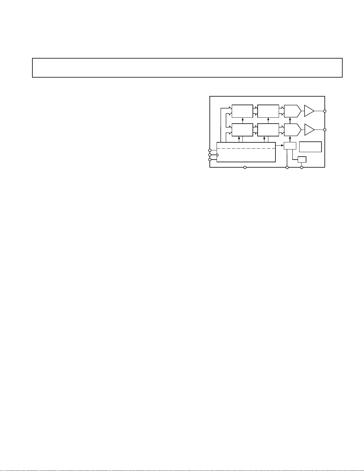
+2.7 V to +5.5 V, Serial Input, Dual
I DAC A
POWER ON
RESET
DIN
SYNC
SCLK
REF
V
DD
AD7303
V
OUT
A
V
OUT
B
GND
I/V
INPUT
REGISTER
MUX
DAC
REGISTER
I/V
INPUT
REGISTER
DAC
REGISTER
÷2
16-BIT SHIFT REGISTER
DATA (8)
CONTROL (8)
I DAC B
a
FEATURES
Two 8-Bit DACs in One Package
8-Pin DIP/SOIC and microSOIC Packages
+2.7 V to +5.5 V Operation
Internal & External Reference Capability
Individual DAC Power-Down Function
Three-Wire Serial Interface
QSPI™, SPI™ and Microwire™ Compatible
On-Chip Output Buffer
Rail-to-Rail Operation
On-Chip Control Register
Low Power Operation: 2.3 mA @ 3.3 V
Full Power-Down to 1 mA max, typically 80 nA
APPLICATIONS
Portable Battery Powered Instruments
Digital Gain and Offset Adjustment
Programmable Voltage and Current Sources
Programmable Attenuators
Voltage Output 8-Bit DAC
AD7303
FUNCTIONAL BLOCK DIAGRAM
GENERAL DESCRIPTION
The AD7303 is a dual, 8-bit voltage out DAC that operates
from a single +2.7 V to +5.5 V supply. Its on-chip precision output buffers allow the DAC outputs to swing rail to rail. This device uses a versatile 3-wire serial interface that operates at clock
rates up to 30 MHz, and is compatible with QSPI, SPI, microwire
and digital signal processor interface standards. The serial input
register is sixteen bits wide; 8 bits act as data bits for the DACs,
and the remaining eight bits make up a control register.
The on-chip control register is used to address the relevant
DAC, to power down the complete device or an individual
DAC, to select internal or external reference and to provide a
synchronous loading facility for simultaneous update of the
DAC outputs with a software LDAC function.
The low power consumption of this part makes it ideally suited
to portable battery operated equipment. The power consumption is 7.5 mW max at 3 V, reducing to less than 3 µW in full
power-down mode.
The AD7303 is available in an 8-pin plastic dual in-line package, 8-lead SOIC and microSOIC packages.
QSPI and SPI are trademarks of Motorola.
Microwire is a trademark of National Semiconductor.
PRODUCT HIGHLIGHTS
1. Low power, single supply operation. This part operates from
a single +2.7 V to +5.5 V supply and consumes typically
15 mW at 5.5 V, making it ideal for battery powered
applications.
2. The on-chip output buffer amplifiers allow the outputs of the
DACs to swing rail to rail with a settling time of typically 1.2 µs.
3. Internal or external reference capability.
4. High speed serial interface with clock rates up to 30 MHz.
5. Individual power-down of each DAC provided. When completely powered down, the DAC consumes typically 80 nA.
REV. 0
Information furnished by Analog Devices is believed to be accurate and
reliable. However, no responsibility is assumed by Analog Devices for its
use, nor for any infringements of patents or other rights of third parties
which may result from its use. No license is granted by implication or
otherwise under any patent or patent rights of Analog Devices.
One Technology Way, P.O. Box 9106, Norwood, MA 02062-9106, U.S.A.
Tel: 617/329-4700 World Wide Web Site: http://www.analog.com
Fax: 617/326-8703 © Analog Devices, Inc., 1997

(VDD = +2.7 V to +5.5 V, Internal Reference; RL = 10 kV to VDD and GND; CL = 100 pF
AD7303–SPECIFICATIONS
Parameter B Versions
to GND; all specifications T
1
Units Conditions/Comments
MIN
to T
unless otherwise noted)
MAX
STATIC PERFORMANCE
Resolution 8 Bits
Relative Accuracy ±1 LSB max Note 2
Differential Nonlinearity ±1 LSB max Guaranteed Monotonic
Zero-Code Error @ +25°C 3 LSB max All Zeros Loaded to DAC Register
Full-Scale Error –0.5 LSB typ All Ones Loaded to DAC Register
Gain Error
3
+1 % FSR typ
Zero-Code Temperature Coefficient 100 µV/°C typ
DAC REFERENCE INPUT
REFIN Input Range 1 to V
REFIN Input Impedance 10 ΜΩ typ
Internal Voltage Reference Error
4
±1 % max
/2 V min to max
DD
OUTPUT CHARACTERISTICS
Output Voltage Range 0 to V
DD
V min to max
Output Voltage Settling Time 2 µs max Typically 1.2 µs
Slew Rate 7.5 V/µs typ
Digital to Analog Glitch Impulse 0.5 nV-s typ 1 LSB Change Around Major Carry
Digital Feedthrough 0.2 nV-s typ
Digital Crosstalk 0.2 nV-s typ
Analog Crosstalk ±0.2 LSB typ
DC Output Impedance 40 Ω typ
Short Circuit Current 14 mA typ
Power Supply Rejection Ratio 0.0001 %/% max ∆ VDD = ±10%
LOGIC INPUTS
Input Current ±10 µA max
V
, Input Low Voltage 0.8 V max VDD = +5 V
INL
V
, Input High Voltage 2.4 V min VDD = +5 V
INH
0.6 V max V
2.1 V min V
= +3 V
DD
= +3 V
DD
Pin Capacitance 5 pF max
POWER REQUIREMENTS
V
DD
I
(Normal Mode) Both DACs Active and Excluding Load Currents,
DD
V
= 3.3 V VIH = VDD, VIL = GND
DD
2.7/5.5 V min/max
@ +25°C 2.1 mA max See Figure 8
T
V
MIN
DD
– T
= 5.5 V
MAX
2.3 mA max
@ +25°C 2.7 mA max
T
– T
MIN
I
(Full Power-Down)
DD
MAX
@ +25°C 80 nA typ V
T
– T
MIN
MAX
NOTES
1
Temperature ranges are as follows: B Version, –40°C to +105°C.
2
Relative Accuracy is calculated using a reduced digital code range of 15 to 245.
3
Gain Error is specified between Codes 15 and 245. The actual error at Code 15 is typically 3 LSB.
4
Internal Voltage Reference Error = (Actual V
is selected.
Specifications subject to change without notice.
REF
3.5 mA max
1 µA max See Figure 19
– Ideal V
REF
/Ideal V
) • 100. Ideal V
REF
= VDD/2, actual V
REF
= VDD, VIL = GND
IH
= voltage on reference pin when internal reference
REF
ORDERING GUIDE
Temperature Package
Model Range Options*
AD7303BN –40°C to +105°C N-8
AD7303BR –40°C to +105°C SO-8
AD7303BRM –40°C to +105°C RM-8
*N = Plastic DIP; R = SOIC; RM = microSOIC.
–2–
REV. 0
AD7303
(VDD = +2.7 V to +5.5 V; GND = 0 V; Reference = Internal VDD/2 Reference; all specifications
1, 2
T
to T
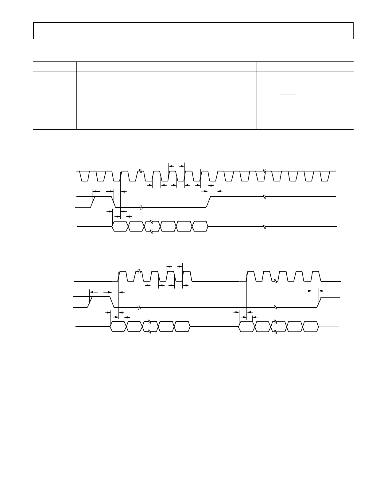
TIMING CHARACTERISTICS
Parameter Limit at T
t
1
t
2
t
3
t
4
t
5
t
6
t
7
t
8
NOTES
1
Sample tested at +25°C to ensure compliance. All input signals are specified with tr = tf = 5 ns (10% to 90% of VDD) and timed from a voltage level of (VIL + VIH)/2,
tr and tf should not exceed 1 µs on any input.
2
See Figures 1 and 2.
33 ns min SCLK Cycle Time
13 ns min SCLK High Time
13 ns min SCLK Low Time
5 ns min SYNC Setup Time
5 ns min Data Setup Time
4.5 ns min Data Hold Time
4.5 ns min SYNC Hold Time
33 ns min Minimum SYNC High Time
MIN
, T
MIN
(B Version) Units Conditions/Comments
MAX
SCLK (I)
t
t
8
4
SYNC (I)
t
5
t
6
DIN (I)
DB15
unless otherwise noted)
MAX
t
1
t
2
t
3
DB0
t
7
t
4
SCLK (I)
SYNC (I)
DIN (I)
Figure 1. Timing Diagram for Continuous 16-Bit Write
t
t
t
4
8
t
5
t
6
DB15 DB8
Figure 2. Timing Diagram for 2 × 8-Bit Writes
t
1
t
2
3
t
5
t
6
DB7 DB0
t
7
REV. 0
–3–
AD7303
WARNING!
ESD SENSITIVE DEVICE
ABSOLUTE MAXIMUM RATINGS*
(TA = +25°C unless otherwise noted)
VDD to GND . . . . . . . . . . . . . . . . . . . . . . . . . . –0.3 V to +7 V
Reference Input Voltage to GND . . . . –0.3 V to V
Digital Input Voltage to GND . . . . . . . –0.3 V to V
V
OUT
A, V
B to GND . . . . . . . . . . . –0.3 V to VDD + 0.3 V
OUT
+ 0.3 V
DD
+ 0.3 V
DD
Operating Temperature Range
Commercial (B Version) . . . . . . . . . . . . . –40°C to +105°C
Storage Temperature Range . . . . . . . . . . . . –65°C to +150°C
Junction Temperature . . . . . . . . . . . . . . . . . . . . . . . . . +150°C
Plastic DIP Package, Power Dissipation . . . . . . . . . . 800 mW
θ
Thermal Impedance . . . . . . . . . . . . . . . . . . . . . 117°C/W
JA
Lead Temperature (Soldering, 10 sec) . . . . . . . . . . . +260°C
SOIC Package, Power Dissipation . . . . . . . . . . . . . . . 450 mW
θ
Thermal Impedance . . . . . . . . . . . . . . . . . . . . . 157°C/W
JA
Lead Temperature, Soldering
Vapor Phase (60 sec) . . . . . . . . . . . . . . . . . . . . . . +215°C
Infrared (15 sec) . . . . . . . . . . . . . . . . . . . . . . . . . . +220°C
MicroSOIC Package, Power Dissipation . . . . . . . . . . 450 mW
θ
Thermal Impedance . . . . . . . . . . . . . . . . . . . . . 206°C/W
JA
Lead Temperature, Soldering
Vapor Phase (60 sec) . . . . . . . . . . . . . . . . . . . . . . +215°C
Infrared (15 sec) . . . . . . . . . . . . . . . . . . . . . . . . . . +220°C
*Stresses above those listed under “Absolute Maximum Ratings” may cause
permanent damage to the device. This is a stress rating only; functional operation
of the device at these or any other conditions above those listed in the operational
sections of this specification is not implied. Exposure to absolute maximum rating
conditions for extended periods may affect device reliability.
CAUTION
ESD (electrostatic discharge) sensitive device. Electrostatic charges as high as 4000 V readily
accumulate on the human body and test equipment and can discharge without detection.
Although the AD7303 features proprietary ESD protection circuitry, permanent damage may
occur on devices subjected to high energy electrostatic discharges. Therefore, proper ESD
precautions are recommended to avoid performance degradation or loss of functionality.
PIN CONFIGURATIONS
(DIP, SOIC and microSOIC)
B
V
1
V
A
OUT
V
2
DD
AD7303
TOP VIEW
3
GND
(Not to Scale)
REF
4
8
OUT
7
SYNC
6
DIN
5
SCLK
PIN FUNCTION DESCRIPTIONS
Pin
No. Mnemonic Function
1V
2V
A Analog Output Voltage from DAC A. The output amplifier swings rail to rail on its output.
OUT
DD
Power Supply Input. These parts can be operated from +2.7 V to +5.5 V and should be decoupled to GND.
3 GND Ground reference point for all circuitry on the part.
4 REF External Reference Input. This can be used as the reference for both DACs, and is selected by setting the
INT/EXT bit in the control register to a logic one. The range on this reference input is 1 V to VDD/2. When
the internal reference is selected, this voltage will appear as an output for decoupling purposes at the REF Pin.
When using the internal reference, external voltages should not be connected to the REF Pin, see Figure 21.
5 SCLK Serial Clock. Logic Input. Data is clocked into the input shift register on the rising edge of the serial clock
input. Data can be transferred at rates up to 30 MHz.
6 DIN Serial Data Input. This device has a 16-bit shift register, 8 bits for data and 8 bits for control. Data is clocked
into the register on the rising edge of the clock input.
7
SYNC Level Triggered Control Input (active low). This is the frame synchronization signal for the input data. When
8V
SYNC goes low, it enables the input shift register and data is transferred in on the rising edges of the following
clocks. The rising edge of the
B Analog output voltage from DAC B. The output amplifier swings rail to rail on its output.
OUT
SYNC causes the relevant registers to be updated.
–4–
REV. 0

AD7303
TERMINOLOGY
INTEGRAL NONLINEARITY
For the DACs, relative accuracy or endpoint nonlinearity is a
measure of the maximum deviation, in LSBs, from a straight
line passing through the endpoints of the DAC transfer function. A graphical representation of the transfer curve is shown
in Figure 15.
DIFFERENTIAL NONLINEARITY
Differential nonlinearity is the difference between the measured
change and the ideal 1 LSB change of any two adjacent codes. A
specified differential nonlinearity of ±1 LSB maximum ensures
monotonicity.
ZERO CODE ERROR
Zero code error is the measured output voltage from V
OUT
of
either DAC when zero code (all zeros) is loaded to the DAC
latch. It is due to a combination of the offset errors in the DAC
and output amplifier. Zero-scale error is expressed in LSBs.
GAIN ERROR
This is a measure of the span error of the DAC. It is the deviation in slope of the DAC transfer characteristic from ideal
expressed as a percent of the full-scale value. Gain error is calculated between Codes 15 and 245.
FULL-SCALE ERROR
Full-Scale Error is a measure of the output error when the DAC
latch is loaded with FF Hex. Full-scale error includes the offset
error.
DIGITAL-TO-ANALOG GLITCH IMPULSE
Digital-to-analog glitch impulse is the impulse injected into the
analog output when the digital inputs change state with the
DAC selected and the software LDAC used to update the DAC.
It is normally specified as the area of the glitch in nV-s and is
measured when the digital input code is changed by 1 LSB at
the major carry transition.
DIGITAL FEEDTHROUGH
Digital feedthrough is a measure of the impulse injected into the
analog output of a DAC from the digital inputs of the same
DAC, but is measured when the DAC is not updated. It is
specified in nV-s and measured with a full-scale code change on
the data bus, i.e., from all 0s to all 1s and vice versa.
DIGITAL CROSSTALK
Digital crosstalk is the glitch impulse transferred to the output
of one converter due to a digital code change to another DAC.
It is specified in nV-s.
ANALOG CROSSTALK
Analog crosstalk is a change in output of any DAC in response
to a change in the output of the other DAC. It is measured in
LSBs.
POWER SUPPLY REJECTION RATIO (PSRR)
This specification indicates how the output of the DAC is
affected by changes in the power supply voltage. Power supply
rejection ratio is quoted in terms of % change in output per %
of change in V
for full-scale output of the DAC. VDD is varied
DD
± 10%. This specification applies to an external reference only
because the output voltage will track the V
voltage when in-
DD
ternal reference is selected.
REV. 0
–5–

AD7303–Typical Performance Characteristics
SYNC
V
OUT
POWER UP TIME
V
DD
= +5V
INTERNAL REFERENCE
BOTH DACS IN POWER DOWN INITIALLY
1
2
CH1 = 2V/div, CH2 = 5V/div,
TIME BASE = 2µs/div
800
VDD = +5V AND +3V
720
INTERNAL REFERENCE
640
T
= 258C
A
DAC LOADED WITH 00HEX
560
480
– mV
400
OUT
320
V
249
160
80
0
08246
SINK CURRENT – mA
Figure 3. Output Sink Current Capability with V
0.5
0.45
0.4
0.35
0.3
0.25
0.2
ERROR – LSBs
0.15
0.1
0.05
0
1 1.2 2.8
= 3 V and VDD = 5 V
DD
VDD = +5V
= 258C
T
A
INL ERROR
DNL ERROR
1.4 1.6 1.8 2.2 2.4 2.62
REFERENCE VOLTAGE – Volts
5
4.92
4.84
4.76
4.68
4.6
– Volts
4.52
OUT
V
4.44
V
= +5V
DD
4.36
INTERNAL REFERENCE
DAC REGISTER LOADED WITH FFHEX
4.28
TA = 25°C
4.2
02 846
SOURCE CURRENT – mA
Figure 4. Output Source Current
Capability with V
5
4.5
4
INTERNAL REFERENCE
VDD = +5V
3.5
– mA
DD
I
3
2.5
2
–60 –40 –20 0 20 40 60 80 100 120 140
LOGIC INPUTS = V
TEMPERATURE – 8C
= 5 V
DD
LOGIC INPUTS = VIH OR V
OR GND
DD
IL
3.5
3.25
3
2.75
2.5
2.25
– Volts
VDD = +3V
2
OUT
INTERNAL REFERENCE
V
DAC REGISTER LOADED WITH FFHEX
1.75
TA = 25°C
1.5
1.25
1
01 8234567
SOURCE CURRENT – mA
Figure 5. Output Source Current
Capability with V
5.5
5
INTERNAL REFERENCE
4.5
3.5
– mA
DD
I
2.5
1.5
TA = 25°C
4
LOGIC INPUTS = VIH OR V
3
2
2.5 3 5.5
= 3 V
DD
IL
LOGIC INPUTS = V
3.5 4 4.5 5
V
DD
DD
– Volts
OR GND
Figure 6. Relative Accuracy vs.
External Reference
10
5
0
–5
–10
–15
VDD = +5V
–20
EXTERNAL SINE WAVE REFERENCE
DAC REGISTER LOADED WITH FFHEX
–25
TA = 25°C
ATTENUATION – dB
–30
–35
–40
1 10 10000100 1000
FREQUENCY – kHz
Figure 9. Large Scale Signal
Frequency Response
Figure 7. Supply Current vs.
Temperature
T
V
= +3V
SYNC
DD
1
INTERNAL VOLTAGE REFERENCE
FULL SCALE CODE CHANGE 00H-FFH
TA = 25°C
2
V
OUT
V
OUT
3
CH1 5V, CH2 1V, CH3 20mV
TIME BASE = 200ns/div
Figure 10. Full-Scale Settling Time
Figure 8. Supply Current vs.
Supply Voltage
Figure 11. Exiting Power-Down (Full
Power-Down)
–6–
REV. 0

AD7303
2
1
V
OUT
CH1 5.00V, CH2 50.0mV, M 250ns
SYNC
V
DD
= +5V
INTERNAL VOLTAGE
REFERENCE
10 LSB STEP CHANGE
T
A
= 258C
V
DD
= +5V
INTERNAL REFERENCE
0.5
0.4
0.3
0.2
0.1
0
–0.1
–0.2
–0.3
–0.4
–0.5
–60 –40 –20 0 20 40 60 80 100 120 140
TEMPERATURE – 8C
DNL ERROR – LSB
TEMPERATURE – 8C
500
400
200
100
0
300
–50 0
50 100 150
VDD = +5.5V
V
IL
AND VIH = 0V OR V
DD
POWER-DOWN CURRENT – nA
–25 25 75 125
VDD = +5V
INTERNAL REFERENCE
= 258C
T
A
T
DAC A = NORMAL OPERATION
SYNC
2
1
DAC B INITIALLY IN POWER
DOWN
V
B
OUT
CH1 2V, CH2 5V, M 500ns
DAC B EXITING
POWER DOWN
Figure 12. Exiting Power-Down
(Partial Power-Down)
0.5
V
= +5V
DD
0.4
INTERNAL REFERENCE
5kΩ 100pF LOAD
0.3
LIMITED CODE RANGE (10-245)
= 25°C
T
A
0.2
0.1
0
–0.1
–0.2
INL ERROR – LSB
–0.3
–0.4
–0.5
DAC B
0 25532 64 96 128 160 192 224
Input Code (10 to 245)
DAC A
Figure 15. Integral Linearity Plot
7
6
←
5
4
– mA
DD
3
I
2
VDD = +3V
1
0
050.5 1 1.5 2 2.5 3 3.5 4 4.5
VDD = +5V
Figure 13. Supply Current vs.
Logic Input Voltage
0.5
0.4
0.3
0.2
0.1
V
= +5V
DD
INTERNAL REFERENCE
0
–0.1
INL ERROR – LSB
–0.2
–0.3
–0.4
–0.5
–60 –40 –20 0 20 40 60 80 100 120 140
TEMPERATURE – 8C
Figure 16. Typical INL vs.
Temperature
Figure 14. Small Scale Settling
Time
Figure 17. Typical DNL vs.
Temperature
REV. 0
1.0
0.8
V
= +5V
DD
0.6
0.4
0.2
INT REFERENCE ERROR – 6%
0
–60 –40 –20 0 20 40 60 80 100 120 140
TEMPERATURE – 8C
Figure 18. Typical Internal Reference
Error vs. Temperature
Figure 19. Power-Down Current vs.
Temperature
–7–

AD7303
GENERAL DESCRIPTION
D/A Section
The AD7303 is a dual 8-bit voltage output digital-to-analog
converter. The architecture consists of a reference amplifier and
a current source DAC, followed by a current-to-voltage converter capable of generating rail-to-rail voltages on the output of
the DAC. Figure 20 shows a block diagram of the basic DAC
architecture.
REF
V
DD
30kΩ
30kΩ
REFERENCE
AMPLIFIER
AD7303
CURRENT
DAC
11.7kΩ
11.7kΩ
OUTPUT
AMPLIFIER
V
A/B
O
Figure 20. DAC Architecture
Both DAC A and DAC B outputs are internally buffered and
these output buffer amplifiers have rail-to-rail output characteristics. The output amplifier is capable of driving a load of 10 kΩ
to both V
and ground and 100 pF to ground. The reference
DD
selection for the DAC can be either internally generated from
V
or externally applied through the REF pin. Reference
DD
selection is via a bit in the control register. The range on the
external reference input is from 1.0 V to V
/2. The output
DD
voltage from either DAC is given by:
V
A/B = 2 × V
O
× (N/256)
REF
where:
V
is the voltage applied to the external REF pin or
REF
V
/2 when the internal reference is selected.
DD
N is the decimal equivalent of the code loaded to the DAC
register and ranges from 0 to 255.
Reference
The AD7303 has the facility to use either an external reference
applied through the REF pin or an internal reference generated
from V
where the internal V
. Figure 21 shows the reference input arrangement
DD
/2 has been selected.
DD
reference appears at the reference pin as an output voltage for
decoupling purposes. When using the internal reference, external
references should not be connected to the REF pin. If external reference is selected, both switches are open and the externally
applied voltage to the REF pin is applied to the reference amplifier.
Decoupling capacitors applied to the REF pin decouple both
the internal reference and external reference. In noisy environments it is recommended that a 0.1 µF capacitor be connected
to the REF pin to provide added decoupling even when the internal reference is selected.
Analog Outputs
The AD7303 contains two independent voltage output DACs
with 8-bit resolution and rail-to-rail operation. The output buffer
provides a gain of two at the output. Figures 3 to 5 show the sink
and source capabilities of the output amplifier. The slew rate of the
output amplifier is typically 8 V/µs and has a full-scale settling to 8
bits with a 100 pF capacitive load in typically 1.2 µs.
The input coding to the DAC is straight binary. Table I shows
the binary transfer function for the AD7303. Figure 22 shows
the DAC transfer function for binary coding. Any DAC output
voltage can ideally be expressed as:
V
OUT
= 2 × V
(N/256)
REF
where:
N is the decimal equivalent of the binary input code.
N ranges from 0 to 255.
V
is the voltage applied to the external REF pin when
REF
the external reference is selected and is V
/2 if the
DD
internal reference is used.
Table I. Binary Code Table for AD7303 DAC
Digital Input
MSB . . . LSB Analog Output
1111 1111 2 × 255/256 × V
1111 1110 2 × 254/256 × V
1000 0001 2 × 129/256 × V
1000 0000 V
REF
V
0111 1111 2 × 127/256 × V
0000 0001 2 × V
REF
/256 V
REF
REF
REF
REF
V
V
V
V
0000 0000 0 V
AD7303
INT/EXT
REFERENCE
AMPLIFIER
0.1µF
REF
30kΩ
30kΩ
V
DD
Figure 21. Reference Input
When the internal reference is selected during the write to the
DAC, both switches are closed and V
applied to the reference amplifier. This internal V
/2 is generated and
DD
/2 reference
DD
appears at the reference pin as an output voltage for decoupling
purposes. When using the internal reference, external references
should not be connected to the REF Pin. This internal V
DD
/2
–8–
2.V
REF
V
REF
DAC OUTPUT VOLTAGE
0
DAC INPUT
CODE
Figure 22. DAC Transfer Function
00 01
FF80 81 FE7F
REV. 0

AD7303
SERIAL INTERFACE
The AD7303 contains a versatile 3-wire serial interface that is
compatible with SPI, QSPI and Microwire interface standards as well as a host of digital signal processors. An active
low SYNC enables the shift register to receive data from the
serial data input DIN. Data is clocked into the shift register on
the rising edge of the serial clock. The serial clock frequency
can be as high as 30 MHz. This shift register is 16 bits wide as
shown in Figures 23 and 24. The first eight bits are control bits
and the second eight bits are data bits for the DACs. Each
transfer must consist of a 16-bit transfer. Data is sent MSB first
and can be transmitted in one 16-bit write or two 8-bit writes.
SPI and Microwire interfaces output data in 8-bit bytes and
thus require two 8-bit transfers. In this case the SYNC input to
the DAC should remain low until all sixteen bits have been
transferred to the shift register. QSPI interfaces can be pro-
INT/EXT
MSB
X
LDAC
PDB
PDA
A/B
CR1
CR0
DB7
DB6
16-BIT SHIFT REGISTER
DB5
DB4
DB3
DB2
DB1
LSB
DB0
SYNC
LATCH
7
8
8
8
SEQUENCER
LATCH & CLK
DRIVERS
CLOCK BUS
INPUT
REGISTER
INPUT
REGISTER
16
8
8
DAC A POWER-DOWN
DAC B POWER-DOWN
BANDGAP POWER-DOWN
8 TO 32
DECODER
8 TO 32
DECODER
grammed to transfer data in 16-bit words. After clocking all sixteen bits to the shift register, the rising edge of SYNC executes
the programmed function. The DACs are double buffered
which allows their outputs to be simultaneously updated.
INPUT SHIFT REGISTER DESCRIPTION
The input shift register is 16 bits wide. The first eight bits consist of control bits and the last eight bits are data bits. Figure 23
shows a block diagram of the logic interface on the AD7303
DAC. The seven bits in the control word are taken from the input shift register to a latch sequencer that decodes this data and
provides output signals that control the data transfers to the input and data registers of the selected DAC, as well as output
updating and various power-down features associated with the
control section. A description of all bits contained in the input
shift register is given below.
DAC A BIAS
DAC B BIAS
V
A
OUT
V
B
OUT
REF
SELECTOR
REFERENCE
30
30
INT
CURRENT
SWITCH
DAC
REGISTER
DAC
REGISTER
BANDGAP
BIAS GEN
REF
RESISTOR
SWITCH
30
30
DAC A
DAC B
REV. 0
SYNC
SCLK
DIN
Figure 23. Logic Interface on the AD7303
–9–

AD7303
DB15 (MSB) DB0 (LSB)
INT/EXT
|––––––––––––––––––––––––– Control Bits –––––––––––––––––––––––––|––––––––––––––––––––––––– Data Bits –––––––––––––––––––––––––|
Bit Location Mnemonic Description
X LDAC PDB PBA
Figure 24. Input Shift Register Contents
CR1 CR0 DB7 DB6 DB5 DB4 DB3 DB2 DB1 DB0
A/B
DB15
DB14 X Uncommitted bit.
DB13 LDAC Load DAC bit for synchronous update of DAC outputs.
DB12 PDB Power-down DAC B.
DB11 PDA Power-down DAC A.
DB10
DB9 CR1 Control Bit 1 used in conjunction with CR0 to implement the various data loading functions.
DB8 CR0 Control Bit 0 used in conjunction with CR1 to implement the various data loading functions.
DB7–DB0 Data These bits contain the data used to update the output of the DACs. DB7 is the MSB and
CONTROL BITS
LDAC A/B CR1 CR0 Function Implemented
0 X 0 0 Both DAC registers loaded from shift register.
0 0 0 1 Update DAC A input register from shift register.
0 1 0 1 Update DAC B input register from shift register.
0 0 1 0 Update DAC A DAC register from input register.
0 1 1 0 Update DAC B DAC register from input register.
0 0 1 1 Update DAC A DAC register from shift register.
0 1 1 1 Update DAC B DAC register from shift register.
1 0 X X Load DAC A input register from shift register and update
1 1 X X Load DAC B input register from shift register and update
INT/EXT Selects between internal and external reference.
A/B Address bit to select either DAC A or DAC B.
DB0 the LSB of the 8-bit data word.
both DAC A and DAC B DAC registers.
both DAC A and DAC B DAC registers outputs.
INT/EXT Function
0 Internal VDD/2 reference selected.
1 External reference selected; this external reference is applied at the REF pin and ranges from
1 V to VDD/2.
PDA PDB Function
0 0 Both DACs active.
0 1 DAC A active and DAC B in power-down mode.
1 0 DAC A in power-down mode and DAC B active.
1 1 Both DACs powered down.
–10–
REV. 0

AD7303
SCLK
68HC11/68L11*
SCK
*ADDITIONAL PINS OMITTED FOR CLARITY
SYNC
DIN
MOSI
AD7303*
PC7
SCLK
80C51/80L51*
TXD
*ADDITIONAL PINS OMITTED FOR CLARITY
SYNC
SDIN
RXD
AD7303*
P3.3
POWER-ON RESET
The AD7303 has a power-on reset circuit designed to allow output
stability during power-up. This circuit holds the DACs in a reset
state until a write takes place to the DAC. In the reset state all zeros
are latched into the input registers of each DAC, and the DAC registers are in transparent mode. Thus the output of both DACs are
held at ground potential until a write takes place to the DAC.
POWER-DOWN FEATURES
Two bits in the control section of the 16-bit input word are used to
put the AD7303 into low power mode. DAC A and DAC B can be
powered down separately. When both DACs are powered down,
the current consumption of the device is reduced to less than 1 µA,
making the device suitable for use in portable battery powered
equipment. The reference bias servo loop, the output amplifiers
and associated linear circuitry are all shut down when the powerdown is activated. The output sees a load of approximately 23 kΩ
to GND when in power-down mode as shown in Figure 25. The
contents of the data registers are unaffected when in power-down
mode. The time to exit power-down is determined by the nature of
the power-down, if the device is fully powered down the bias generator is also powered down and the device takes typically 13 µs to
exit power-down mode. If the device is only partially powered
down, i.e., only one channel powered down, in this case the bias
generator is active and the time required for the power-down channel to exit this mode is typically 1.6 µs. See Figures 11 and 12.
V
DD
VO A/B
I
V
11.7kΩ
DAC
11.7kΩ
REF
Figure 25. Output Stage During Power-Down
MICROPROCESSOR INTERFACING
AD7303 to ADSP-2101/ADSP-2103 Interface
Figure 26 shows a serial interface between the AD7303 and the
ADSP-2101/ADSP-2103. The ADSP-2101/ADSP-2103 should
be set up to operate in the SPORT Transmit Alternate Framing
Mode. The ADSP-2101/ADSP-2103 SPORT is programmed
through the SPORT control register and should be configured
as follows: Internal Clock Operation, Active Low Framing,
16-Bit Word Length. Transmission is initiated by writing a word
to the Tx register after the SPORT has been enabled. The data
is clocked out on each falling edge of the serial clock and clocked
into the AD7303 on the rising edge of the SCLK.
AD7303 to 68HC11/68L11 Interface
Figure 27 shows a serial interface between the AD7303 and the
68HC11/68L11 microcontroller. SCK of the 68HC11/68L11
drives the CLKIN of the AD7303, while the MOSI output
drives the serial data line of the DAC. The
SYNC signal is
derived from a port line (PC7). The setup conditions for correct operation of this interface are as follows: the 68HC11/
68L11 should be configured so that its CPOL bit is a 0 and its
CPHA bit is a 0. When data is being transmitted to the DAC,
the
SYNC line is taken low (PC7). When the 68HC11/68L11 is
configured as above, data appearing on the MOSI output is
valid on the rising edge of SCK. Serial data from the 68HC11/
68L11 is transmitted in 8-bit bytes with only eight falling clock
edges occurring in the transmit cycle. Data is transmitted MSB
first. In order to load data to the AD7303, PC7 is left low after
the first eight bits are transferred, and a second serial write operation is performed to the DAC and PC7 is taken high at the
end of this procedure.
Figure 27. AD7303 to 68HC11/68L11 Interface
AD7303 to 80C51/80L51 Interface
Figure 28 shows a serial interface between the AD7303 and the
80C51/80L51 microcontroller. The setup for the interface is as
follows: TXD of the 80C51/80L51 drives SCLK of the AD7303,
while RXD drives the serial data line of the part. The
SYNC
signal is again derived from a bit programmable pin on the port.
In this case port line P3.3 is used. When data is to be transmitted to the AD7303, P3.3 is taken low. The 80C51/80L51 transmits data only in 8-bit bytes; thus only eight falling clock edges
occur in the transmit cycle. To load data to the DAC, P3.3 is
left low after the first eight bits are transmitted, and a second
write cycle is initiated to transmit the second byte of data. P3.3
is taken high following the completion of this cycle. The 80C51/
80L51 outputs the serial data in a format which has the LSB
first. The AD7303 requires its data with the MSB as the first bit
received. The 80C51/80L51 transmit routine should take this
into account.
ADSP-2101/
ADSP-2103*
SCLK
*ADDITIONAL PINS OMITTED FOR CLARITY
Figure 26. AD7303 to ADSP-2101/ADSP-2103 Interface
REV. 0
TFS
DT
SYNC
DIN
SCLK
AD7303*
Figure 28. AD7303 to 80C51/80L51 Interface
–11–

AD7303
R1
10kΩ
R4
20kΩ
R3
10kΩ
+5V
–5V
±5V
AD7303
V
OUT
A
10µF0.1µF
V
DD
= +5V
V
DD
GND
AD780/ REF192
WITH V
DD
= +5V
OR
AD589 WITH V
DD
= +3V
REF
SCLK
DIN
SYNC
GND
V
OUT
V
IN
0.1µF
SERIAL
INTERFACE
EXT
REF
R2
20kΩ
AD7303 to Microwire Interface
Figure 29 shows an interface between the AD7303 and any
microwire compatible device. Serial data is shifted out on the
falling edge of the serial clock and is clocked into the AD7303
on the rising edge of the SK.
MICROWIRE*
CS
SK
SO
*ADDITIONAL PINS OMITTED FOR CLARITY
AD7303*
SYNC
SCLK
DIN
Figure 29. AD7303 to Microwire Interface
APPLICATIONS
Typical Application Circuit
Figure 30 shows a typical setup for the AD7303 when using an
external reference. The reference range for the AD7303 is from
1 V to V
/2 V. Higher values of reference can be incorporated
DD
but will saturate the output at both the top and bottom end of
the transfer function. From input to output on the AD7303
there is a gain of two. Suitable references for 5 V operation are
the AD780 and REF192. For 3 V operation, a suitable external
reference would be the AD589, a 1.23 V bandgap reference.
VDD = +3V TO +5V
10µF0.1µF
V
IN
EXT
V
OUT
REF
GND
AD780/ REF192
WITH VDD = +5V
OR
AD589 WITH VDD = +3V
0.1µF
SERIAL
INTERFACE
REF
SCLK
DIN
SYNC
V
DD
AD7303
GND
V
V
Figure 30. AD7303 Using External Reference
The AD7303 can also be used with its own internally derived
V
/2 reference. Reference selection is through the INT/EXT
DD
bit of the 16-bit input word. The internal reference, when
selected, is also provided as an output at the REF pin and can
be decoupled at this point with a 0.1 µF capacitor for noise
reduction purposes. AC references can also be applied as external references to the AD7303. The AD7303 has limited multiplying capability, and a multiplying bandwidth of up to 10 kHz
is achievable.
OUT
OUT
Bipolar Operation Using the AD7303
The AD7303 has been designed for single supply operation, but
bipolar operation is achievable using the circuit shown in Figure
31. The circuit shown has been configured to achieve an output
voltage range of –5 V < V
< +5 V. Rail-to-rail operation at the
O
amplifier output is achievable using an AD820 or OP295 as the
output amplifier.
Figure 31. Bipolar Operation Using the AD7303
The output voltage for any input code can be calculated as
follows:
VO = [(1+R4/R3)*(R2/(R1+R2)*(2*V
*D/256)] – R4*V
REF
REF
/R3
where
D is the decimal equivalent of the code loaded to the DAC
and
V
is the reference voltage input.
REF
A
B
With V
V
DD
Opto-Isolated Interface for Process Control Applications
= 2.5 V, R1 = R3 = 10 kΩ and R2 = R4 = 20K and
REF
= 5 V.
V
= (10 × D/256) – 5
OUT
The AD7303 has a versatile 3-wire serial interface making it
ideal for generating accurate voltages in process control and
industrial applications. Due to noise, safety requirements or distance, it may be necessary to isolate the AD7303 from the controller. This can easily be achieved by using opto-isolators,
which will provide isolation in excess of 3 kV. The serial loading
structure of the AD7303 makes it ideally suited for use in optoisolated applications. Figure 32 shows an opto-isolated interface
to the AD7303 where DIN, SCLK and
SYNC are driven from
opto-couplers. In this application the reference for the AD7303
is the internal V
/2 reference. It is being decoupled at the REF
DD
pin with a 0.1 µF ceramic capacitor for noise reduction purposes.
–12–
REV. 0

AD7303
4.7kΩ
470Ω
+5V
LOAD
V
SOURCE
AD7303
V
OUT
A
10µF0.1µF
V
DD
= +5V
V
DD
GND
AD780/ REF192
WITH V
DD
= +5V
REF
SCLK
DIN
SYNC
GND
V
OUT
V
IN
0.1µF
SERIAL
INTERFACE
EXT
REF
AD820/
OP295
+5V
POWER
SCLK
SYNC
DATA
10kΩ
10kΩ
10kΩ
REGULATOR
V
DD
V
DD
V
DD
SCLK
SYNC
DIN
V
DD
AD7303
AGND
10µF
REF
V
OUT
V
OUT
0.1µF
0.1µF
A
B
Figure 32. AD7303 in Opto-Isolated Interface
Decoding Multiple AD7303
The SYNC pin on the AD7303 can be used in applications to
decode a number of DACs. In this application, all DACs in the
system receive the same serial clock and serial data, but only the
SYNC to one of the DACs will be active at any one time allowing access to two channels in this eight-channel system. The
74HC139 is used as a 2- to 4-line decoder to address any of the
DACs in the system. To prevent timing errors from occurring,
the enable input should be brought to its inactive state while the
coded address inputs are changing state. Figure 33 shows a diagram of a typical setup for decoding multiple AD7303 devices in
a system.
AD7303
SYNC
DIN
SCLK
AD7303
SYNC
DIN
SCLK
AD7303
SYNC
DIN
SCLK
AD7303
SYNC
DIN
SCLK
–13–
SCLK
DIN
ENABLE
CODED
ADDRESS
Figure 33. Decoding Multiple AD7303 Devices in a System
REV. 0
1G
1A
1B
74HC139
DGND
V
DD
V
CC
1Y0
1Y1
1Y2
1Y3
AD7303 as a Digitally Programmable Window Detector
A digitally programmable upper/lower limit detector using the
two DACs in the AD7303 is shown in Figure 34. The upper
and lower limits for the test are loaded to DACs A and B which,
in turn, set the limits on the CMP04. If a signal at the V
input
IN
is not within the programmed window, a led will indicate the fail
condition.
+5V
0.1µF
SYNC
DIN
SCLK
0.1µF
REF
SYNC
DIN
SCLK
10µF
AD7303
GND
V
IN
V
DD
V
A
OUT
1/2
CMP04
B
V
OUT
1kΩ
FAIL
PASS/FAIL
1/6 74HC05
1kΩ
PASS
Figure 34. Window Detector Using AD7303
Programmable Current Source
Figure 35 shows the AD7303 used as the control element of a
programmable current source. In this circuit, the full-scale current is set to 1 mA. The output voltage from the DAC is applied
across the current setting resistor of 4.7 kΩ in series with the
full-scale setting resistor of 470 Ω. Suitable transistors to place
in the feedback loop of the amplifier include the BC107 and the
2N3904, which enable the current source to operate from a min
V
of 6 V. The operating range is determined by the oper-
SOURCE
ating characteristics of the transistor. Suitable amplifiers include the AD820 and the OP295, both having rail-to-rail
operation on their outputs. The current for any digital input
code can be calculated as follows:
I = 2 × V
× D/(5E + 3 × 256) mA
REF
Figure 35. Programmable Current Source

AD7303
Power Supply Bypassing and Grounding
In any circuit where accuracy is important, careful consideration
of the power supply and ground return layout helps to ensure
the rated performance. The printed circuit board on which the
AD7303 is mounted should be designed so that the analog and
digital sections are separated, and confined to certain areas of
the board. If the AD7303 is in a system where multiple
devices require an AGND to DGND connection, the connection should be made at one point only. The star ground point
should be established as closely as possible to the AD7303. The
AD7303 should have ample supply bypassing of 10 µF in paral-
lel with 0.1 µF on the supply located as closely to the package as
possible, ideally right up against the device. The 10 µF capaci-
tors are the tantalum bead type. The 0.1 µF capacitor should
have low Effective Series Resistance (ESR) and Effective Series
AD7303 to 68HC11 Interface Program Source Code
*
PORTC EQU $1003 Port C Control Register
* "SYNC, 0, 0, 0, 0, 0, 0, 0"
DDRC EQU $1007 Port C Data Direction
PORTD EQU $1008 Port D Data Register
* "0, 0, 0, SCLK, DIN, 0, 0, 0"
DDRD EQU $1009 Port D Data Direction
SPCR EQU $1028 SPI Control Register
* "SPIE, SPE, DWOM, MSTR, CPOL, CPHA, SPR1, SPR0"
SPSR EQU $1029 SPI Status Register
* "SPIF, WCOL, 0, MODF, 0, 0, 0, 0"
SPDR EQU $102A SPI Data Register, Read Buffer, Write Shifter
*
* SDI RAM Variables: DIN 1 is eight MSBs, Control BYTE
DIN 2 is eight LSBs, Data BYTE
DAC requires 2*8-bit Writes
DIN1 EQU $00 DIN BYTE 1: "
DIN2 EQU $01 DIN BYTE 2: " DB7, DB6, DB5, DB4, DB3, DB2, DB1, DB0"
*
ORG $C000 Start of users ram
INIT LDS #$CFFF Top of C page Ram
*
LDAA #$80 1, 0, 0, 0, 0, 0, 0, 0
* SYNC is High
STAA PORTC Initialize Port C Outputs
LDAA #$80 1, 0, 0, 0, 0, 0, 0, 0
STAA DDRC SYNC enabled as output
*
LDAA #$00 0, 0, 0, 0, 0, 0, 0, 0
* SCLK is low, DIN is low
STAA PORTD Initialize Port D outputs
Inductance (ESI), like the common ceramic types that provide a
low impedance path to ground at high frequencies to handle
transient currents due to internal logic switching.
The power supply lines of the AD7303 should use as large a
trace as possible to provide low impedance paths and reduce the
effects of glitches on the power supply line. Fast switching signals such as clocks should be shielded with digital ground to
avoid radiating noise to other parts of the board, and should
never be run near the reference inputs. Avoid crossover of digital and analog signals. Traces on opposite sides of the board
should run at right angles to each other. This reduces the effects of
feedthrough through the board. A microstrip technique is by far
the best, but not always possible with a double-sided board. In
this technique, the component side of the board is dedicated to
ground plane while signal traces are placed on the solder side.
INT/EXT, X, LDAC, PDB, PBA, A/B, CR1, CR0"
–14–
REV. 0

AD7303
LDAA #$18 0, 0, 0, 1, 1, 0, 0, 0
* SCLK and DIN enabled as outputs
LDAA #$53
STAA SPCR SPI on, Master mode, CPOL=0, CPHA=0, Clock rate =E/32
*
BSR UPDATE Update AD7303 output.
JMP #$E000 Restart.
*
UPDATE PSHX Save relevant registers.
PSHY
PSHA
*
LDAA #$00 Control Word "0, 0, 0, 0, 0, 0, 0, 0"
STAA DIN 1 Load both DAC A and DAC B DAC registers from shift register
with internal reference selected.
LDAA #$AA Data Word "1, 0, 1, 0, 1, 0, 1, 0"
STAA DIN 2
*
LDX #DIN1 Stack pointer at first first byte to send via DIN 1.
LDY #$1000 Stack pointer at on chip registers.
*
BCLR PORTC,Y $80 Assert SYNC.
TRANSFER LDAA 0,X Get BYTE to transfer via SPI.
STAA SPDR Write to DIN register to start transfer.
*
WAIT LDAA SPSR Wait for SPIF to be set to indicate that transfer has been completed.
BPL WAIT SPIF is the MSB of the SPCR. SPIF is automatically reset if in a set
state when the status register is read.
*
INX Increment counter for transfer of second byte.
CPX #DIN 2+1 16 bits transferred?
BNE TRANSFER If not, transfer second BYTE.
*Execute instruction
BSET PORTC,Y $80 Bring SYNC back high.
PULA Restore registers.
PULY
PULX
RTS Return to main program.
REV. 0
–15–

AD7303
0.210 (5.33)
MAX
0.160 (4.06)
0.115 (2.93)
0.022 (0.558)
0.014 (0.356)
0.1574 (4.00)
0.1497 (3.80)
OUTLINE DIMENSIONS
Dimensions shown in inches and (mm).
8-Pin Plastic DIP
(N-8)
0.430 (10.92)
0.348 (8.84)
8
14
PIN 1
0.100
(2.54)
BSC
5
0.280 (7.11)
0.240 (6.10)
0.060 (1.52)
0.015 (0.38)
0.070 (1.77)
0.045 (1.15)
0.130
(3.30)
MIN
SEATING
PLANE
0.325 (8.25)
0.300 (7.62)
0.015 (0.381)
0.008 (0.204)
8-Lead SOIC
(SO-8)
0.1968 (5.00)
0.1890 (4.80)
8
5
0.2440 (6.20)
41
0.2284 (5.80)
C2224–12–1/97
0.195 (4.95)
0.115 (2.93)
0.0098 (0.25)
0.0040 (0.10)
SEATING
PLANE
0.122 (3.10)
0.114 (2.90)
0.006 (0.15)
0.002 (0.05)
SEATING
PLANE
PIN 1
0.0500
(1.27)
BSC
0.122 (3.10)
0.114 (2.90)
8
1
PIN 1
0.0256 (0.65) BSC
0.120 (3.05)
0.112 (2.84)
0.018 (0.46)
0.008 (0.20)
0.0688 (1.75)
0.0532 (1.35)
0.0192 (0.49)
0.0138 (0.35)
0.0098 (0.25)
0.0075 (0.19)
8-Lead microSOIC
(RM-8)
5
0.199 (5.05)
0.187 (4.75)
4
0.043 (1.09)
0.037 (0.94)
0.011 (0.28)
0.003 (0.08)
0.0196 (0.50)
0.0099 (0.25)
8°
0°
0.0500 (1.27)
0.0160 (0.41)
0.120 (3.05)
0.112 (2.84)
33°
27°
x 45°
0.028 (0.71)
0.016 (0.41)
PRINTED IN U.S.A.
–16–
REV. 0
 Loading...