REV. A
Information furnished by Analog Devices is believed to be accurate and
reliable. However, no responsibility is assumed by Analog Devices for its
use, nor for any infringements of patents or other rights of third parties
which may result from its use. No license is granted by implication or
otherwise under any patent or patent rights of Analog Devices.
a
LC2MOS Dual, Complete,
12-Bit/14-Bit Serial DACs
AD7242/AD7244
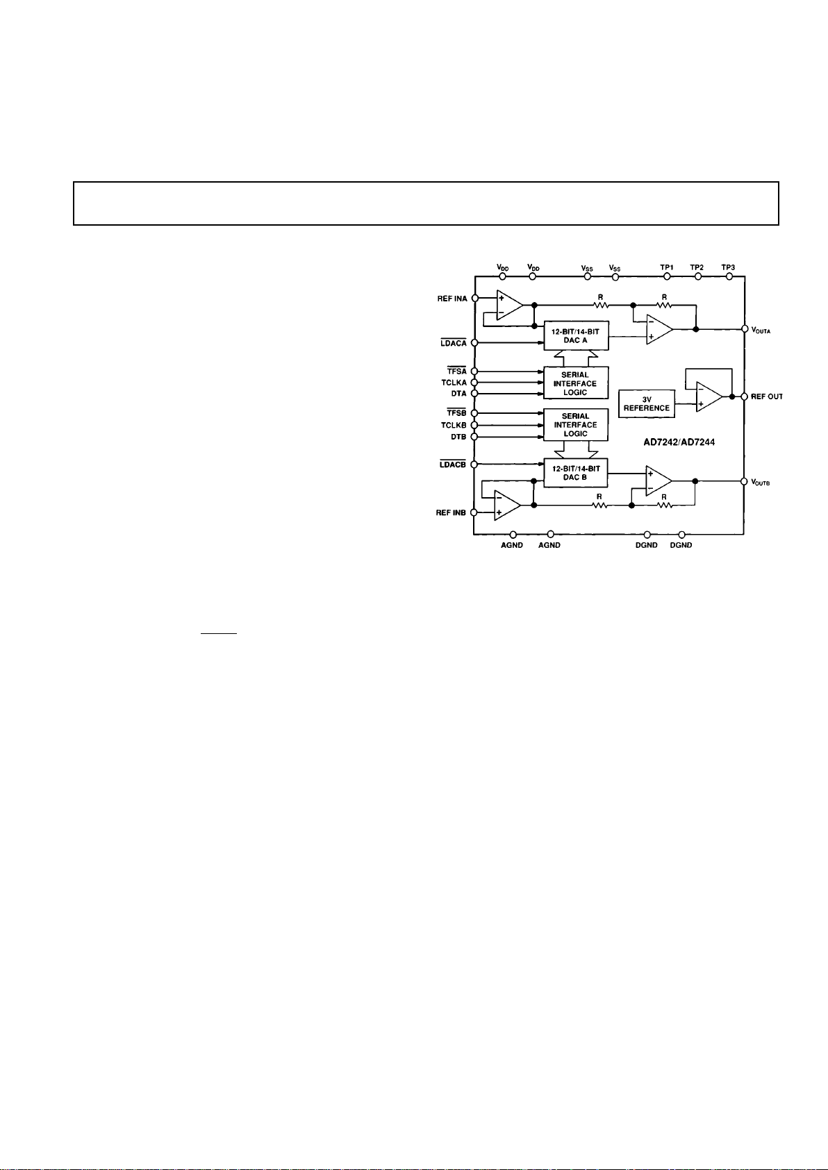
FUNCTIONAL BLOCK DIAGRAM
GENERAL DESCRIPTION
The AD7242/AD7244 is a fast, complete, dual 12-bit/14-bit
voltage output D/A converter. It consists of a 12-bit/14-bit
DAC, 3 V buried Zener reference, DAC output amplifiers and
high speed serial interface logic.
Interfacing to both DACs is serial, minimizing pin count and
allowing a small package size. Standard control signals allow
interfacing to most DSP processors and microcontrollers.
Asynchronous control of DAC updating for both DACs is made
possible with a separate
LDAC input for each DAC.
The AD7242/AD7244 operates from ± 5 V power supplies,
providing an analog output range of ±3 V. A REF OUT/REF
IN function allows the DACs to be driven from the on-chip 3 V
reference or from an external reference source.
The AD7242/AD7244 is fabricated in Linear Compatible
CMOS (LC
2
MOS), an advanced mixed technology process that
combines precision bipolar circuits with low power CMOS
logic. Both parts are available in a 24-pin, 0.3-inch wide, plastic
or hermetic dual-in-line package (DIP) and in a 28-pin, plastic
small outline (SOIC) package. The AD7242 and AD7244 are
available in the same pinout to allow easy upgrade from 12-bit
to 14-bit performance.
FEATURES
Two 12-Bit/14-Bit DACs with Output Amplifiers
AD7242: 12-Bit Resolution
AD7244: 14-Bit Resolution
On-Chip Voltage Reference
Fast Settling Time
AD7242: 3 ms to 61/2 LSB
AD7244: 4 ms to 61/2 LSB
High Speed Serial Interface
Operates from 65 V Supplies
Specified Over –408C to +858C in Plastic Packages
Low Power – 130 mW typ
PRODUCT HIGHLIGHTS
1. Complete, Dual 12-Bit/14-Bit DACs
The AD7242/AD7244 provides the complete function for
generating voltages to 12-bit/14-bit resolution. The part
features an on-chip reference, output buffer amplifiers and
two 12-bit/14-bit D/A converters.
2. High Speed Serial Interface
The AD7242/AD7244 provides a high speed, easy-to-use,
serial interface allowing direct interfacing to DSP processors
and microcontrollers. A separate serial port is provided for
each DAC.
3. Small Package Size
The AD7242/AD7244 is available in a 24-pin DIP and a 28pin SOIC package offering considerable space saving over
comparable solutions.
One Technology Way, P.O. Box 9106, Norwood, MA 02062-9106, U.S.A.
Tel: 617/329-4700 World Wide Web Site: http://www.analog.com
Fax: 617/326-8703 © Analog Devices, Inc., 1996

REV. A
–2–
AD7242/AD7244–SPECIFICATIONS
(VDD = +5 V 6 5% VSS = –5 V 6 5%, AGND = DGND = 0 V, REF INA =
REF INB = +3 V. V
OUTA
, V
OUTB
load to AGND: RL = 2 kV, CL = 100 pF.
All Specifications T
MIN
to T
MAX
unless otherwise noted.)
AD7242
Parameter J, A Versions1K, B Versions1Units Test Conditions/Comments
DC ACCURACY
Resolution 12 12 Bits
Integral Nonlinearity ±1 ±1/2 LSB max
Differential Nonlinearity ±1 ±1 LSB max Guaranteed Monotonic
Bipolar Zero Error ±5 ±5 LSB max
Positive Full-Scale Error
2
±5 ±5 LSB max
Negative Full-Scale Error
2
±5 ±5 LSB max
REFERENCE OUTPUT
3
REF OUT @ +25°C 2.99/3.01 2.99/3.01 V min/V max
T
MIN
to T
MAX
2.98/3.02 2.98/3.02 V min/V max
REF OUT Tempco 35 35 ppm/°C typ
Reference Load Change
(∆REF OUT vs. ∆I) –1 –1 mV max Reference Load Current Change (0 µA–500 µA)
REFERENCE INPUTS
REF INA, REF INB Input Range 2.85/3.15 2.85/3.15 V min/V max 3 V ± 5%
Input Current 1 1 µA max
LOGIC INPUTS
(
LDACA, LDACB, TFSA, TFSB,
TCLKA, TCLKB, DTA, DTB)
Input High Voltage, V
INH
2.4 2.4 V min VDD = 5 V ± 5%
Input Low Voltage, V
INL
0.8 0.8 V max VDD = 5 V ± 5%
Input Current, I
IN
±10 ±10 µA max VIN = 0 V to V
DD
Input Capacitance, C
IN
4
10 10 pF max
ANALOG OUTPUTS
(V
OUTA
, V
OUTB
)
Output Voltage Range ±3 ±3 V nom
DC Output Impedance 0.1 0.1 Ω typ
Short Circuit Current 20 20 mA typ
AC CHARACTERISTICS
4
Voltage Output Settling Time Settling Time to Within ±1/2 LSB of Final Value
Positive Full-Scale Change 3 3 µs max Typically 2 µs
Negative Full-Scale Change 3 3 µs max Typically 2 µs
Digital-to-Analog Glitch Impulse 10 10 nV secs typ DAC Code Change All 1s to All 0s
Digital Feedthrough 2 2 nV secs typ
Channel-to-Channel Isolation 110 110 dB typ V
OUT
= 10 kHz Sine Wave
POWER REQUIREMENTS
V
DD
+5 +5 V nom ±5% for Specified Performance
V
SS
–5 –5 V nom ±5% for Specified Performance
I
DD
27 27 mA max Cumulative Current from the Two VDD Pins
I
SS
15 15 mA max Cumulative Current from the Two VSS Pins
Total Power Dissipation 195 195 mW max Typically 130 mW
NOTES
1
Temperature ranges are as follows: J, K Versions: –40°C to +85°C; A, B Versions: –40°C to +85°C.
2
Measured with respect to REF IN and includes bipolar offset error.
3
For capacitive loads greater than 50 pF, a series resistor is required (see Internal Reference section).
4
Sample tested @ +25°C to ensure compliance.
Specifications subject to change without notice.
AD7242 ORDERING GUIDE
Temperature Integral Package
Model Range Nonlinearity Option*
AD7242JN –40°C to +85°C ±1 LSB max N-24
AD7242KN –40°C to +85°C ±1/2 LSB max N-24
AD7242JR –40°C to +85°C ±1 LSB max R-28
AD7242KR –40°C to +85°C ±1/2 LSB max R-28
AD7242AQ –40°C to +85°C ±1 LSB max Q-24
AD7242BQ –40°C to +85°C ±1/2 LSB max Q-24
*N = Plastic DIP; Q = Cerdip; R = Small Outline IC (SOIC).

AD7244
Parameter J, A Versions1S Version
1
Units Test Conditions/Comments
DC ACCURACY
Resolution 14 14 Bits
Integral Nonlinearity ±2 ±2 LSB max
Differential Nonlinearity ±1 ±1 LSB max Guaranteed Monotonic
Bipolar Zero Error ±10 ±10 LSB max
Positive Full-Scale Error
2
±10 ±10 LSB max
Negative Full-Scale Error
2
±10 ±10 LSB max
REFERENCE OUTPUT
3
REF OUT @ +25°C 2.99/3.01 2.99/3.01 V min/V max
T
MIN
to T
MAX
2.98/3.02 2.98/3.02 V min/V max
REF OUT Tempco 35 35 ppm/°C typ
Reference Load Change
(∆REF OUT vs. ∆I) –1 –1 mV max Reference Load Current Change (0 µA–500 µA)
REFERENCE INPUTS
REF INA, REF INB Input Range 2.85/3.15 2.85/3.15 V min/V max 3 V ± 5%
Input Current 1 1 µA max
LOGIC INPUTS
(
LDACA, LDACB, TFSA, TFSB,
TCLKA, TCLKB, DTA, DTB)
Input High Voltage, V
INH
2.4 2.4 V min VDD = 5 V ± 5%
Input Low Voltage, V
INL
0.8 0.8 V max VDD = 5 V ± 5%
Input Current, I
IN
±10 ±10 µA max VIN = 0 V to V
DD
Input Capacitance, C
IN
4
10 10 pF max
ANALOG OUTPUTS
(V
OUTA
, V
OUTB
)
Output Voltage Range ±3 ±3 V nom
DC Output Impedance 0.1 0.1 Ω typ
Short Circuit Current 20 20 mA typ
AC CHARACTERISTICS
4
Voltage Output Settling Time Settling Time to Within ±1/2 LSB of Final Value
Positive Full-Scale Change 4 4 µs max Typically 2.5 µs
Negative Full-Scale Change 4 4 µs max Typically 2.5 µs
Digital-to-Analog Glitch Impulse 10 10 nV secs typ DAC Code Change All 1s to All 0s
Digital Feedthrough 2 2 nV secs typ
Channel-to-Channel Isolation 110 110 dB typ V
OUT
= 10 kHz Sine Wave
POWER REQUIREMENTS
V
DD
+5 +5 V nom ±5% for Specified Performance
V
SS
–5 –5 V nom ±5% for Specified Performance
I
DD
27 28 mA max Cumulative Current from the Two VDD Pins
I
SS
15 15 mA max Cumulative Current from the Two VSS Pins
Total Power Dissipation 195 205 mW max Typically 130 mW
NOTES
1
Temperature ranges are as follows: J Version: 0°C to +70°C; A Version: –40°C to +85°C; S Version: –55°C to +125°C.
2
Measured with respect to REF IN and includes bipolar offset error.
3
For capacitive loads greater than 50 pF, a series resistor is required (see Internal Reference section).
4
Sample tested @ +25°C to ensure compliance.
Specifications subject to change without notice.
AD7242/AD7244
REV. A
–3–
AD7244 ORDERING GUIDE
Temperature Integral Package
Model
1
Range Nonlinearity Option
2
AD7244JN –40°C to +85°C ±2 LSB max N-24
AD7244JR –40°C to +85°C ±2 LSB max R-28
AD7244AQ –40°C to +85°C ±2 LSB max Q-24
AD7244SQ
3
–55°C to +125°C ±2 LSB max Q-24
NOTES
1
To order MIL-STD-883, Class B, processed parts, add /883B to part number.
Contact local sales office for military data sheet and availability.
2
N = Plastic DIP; Q = Cerdip; R = Small Outline IC (SOIC).
3
This grade will be available to /883B processing only.

AD7242/AD7244
REV. A
–4–
WARNING!
ESD SENSITIVE DEVICE
CAUTION
ESD (electrostatic discharge) sensitive device. Electrostatic charges as high as 4000 V readily
accumulate on the human body and test equipment and can discharge without detection.
Although the AD7242/AD7244 feature proprietary ESD protection circuitry, permanent damage
may occur on devices subjected to high energy electrostatic discharges. Therefore, proper ESD
precautions are recommended to avoid performance degradation or loss of functionality.
TIMING CHARACTERISTICS
1, 2
Limit at T
MIN
, T
MAX
Limit at T
MIN
, T
MAX
Parameter (J, K, A, B Versions) (S Version) Units Conditions/Comments
t
1
50 50 ns min TFS to TCLK Falling Edge
t
2
75 100 ns min TCLK Falling Edge to TFS
t
3
3
150 200 ns min TCLK Cycle Time
t
4
30 40 ns min Data Valid to TCLK Setup Time
t
5
75 100 ns min Data Valid to TCLK Hold Time
t
6
40 40 ns min LDAC Pulse Width
NOTES
1
Timing specifications are sample tested at +25°C to ensure compliance. All input signals are specified with tr = tf = 5 ns (10% to 90% of 5 V) and timed from a volt-
age level of 1.6 V.
2
See Figure 6.
3
TCLK Mark/Space ratio is 40/60 to 60/40.
ABSOLUTE MAXIMUM RATINGS*
(TA = +25°C unless otherwise noted)
VDD to AGND . . . . . . . . . . . . . . . . . . . . . . . . . –0.3 V to +7 V
V
SS
to AGND . . . . . . . . . . . . . . . . . . . . . . . . . +0.3 V to –7 V
AGND to DGND . . . . . . . . . . . . . . . . –0.3 V to V
DD
+ 0.3 V
V
OUT
to AGND . . . . . . . . . . . . . . . . . . . . . . . . . . . . VSS to V
DD
REF OUT to AGND . . . . . . . . . . . . . . –0.3 V to VDD + 0.3 V
REF INA, REF INB to AGND . . . . . . . –0.3 V to V
DD
+ 0.3 V
Digital Inputs to DGND . . . . . . . . . . . . –0.3 V to V
DD
+ 0.3 V
Operating Temperature Range
J, K Versions
AD7244 . . . . . . . . . . . . . . . . . . . . . . . . . . . 0°C to +70°C
AD7242 . . . . . . . . . . . . . . . . . . . . . . . . . –40°C to +85°C
A, B Versions . . . . . . . . . . . . . . . . . . . . . . . –40°C to +85°C
S Version . . . . . . . . . . . . . . . . . . . . . . . . . –55°C to +125°C
(VDD = +5 V 6 5%, VSS = –5 V 6 5%, AGND = DGND = 0 V)
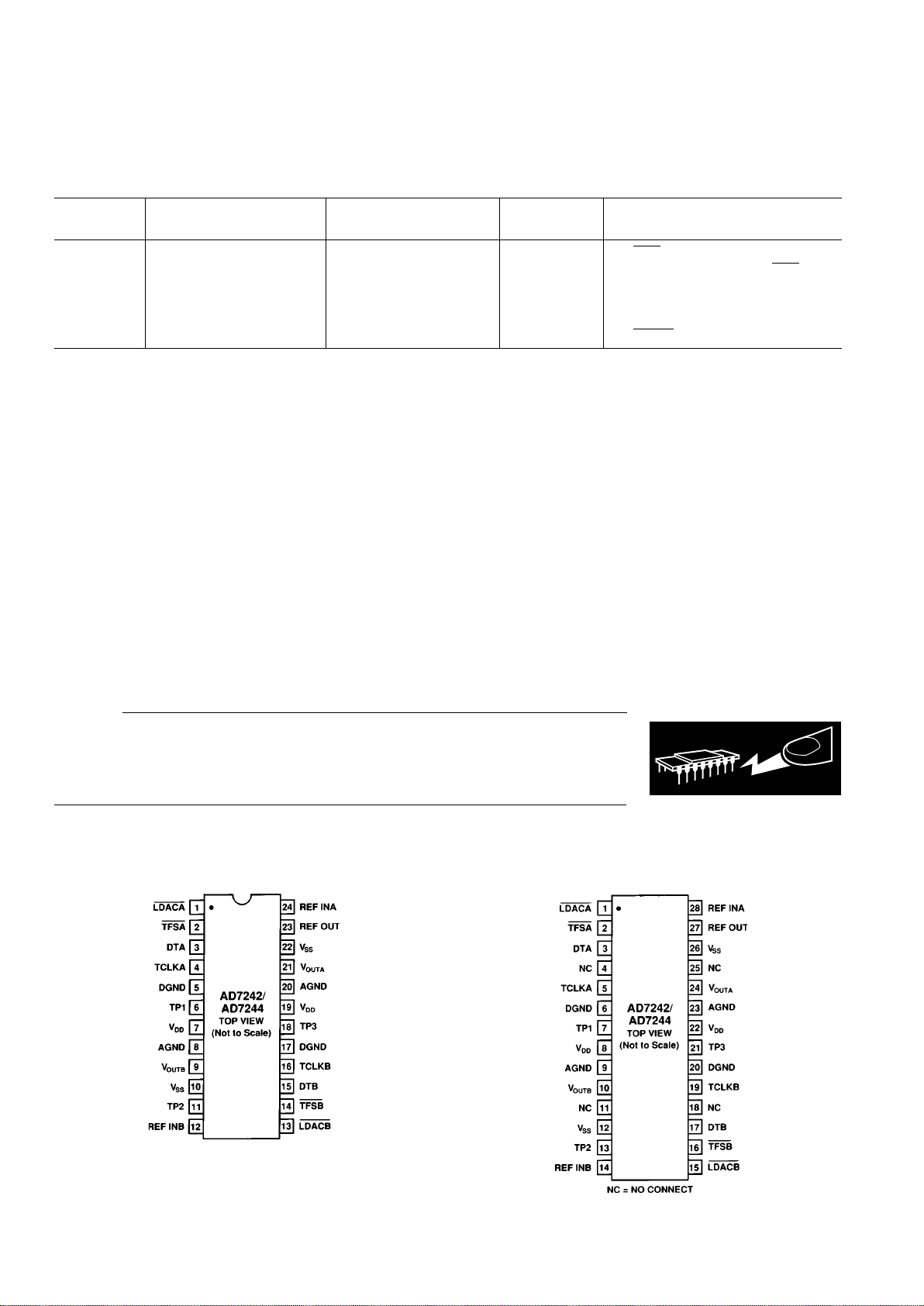
PIN CONFIGURATIONS
Storage Temperature Range . . . . . . . . . . . . –65°C to +150°C
Lead Temperature (Soldering, 10 sec) . . . . . . . . . . . . +300°C
Power Dissipation (Any Package) to +75°C . . . . . . . 550 mW
Derates above +75°C by . . . . . . . . . . . . . . . . . . . . . 6 mW/°C
*Stresses above those listed under “Absolute Maximum Ratings” may cause
permanent damage to the device. This is a stress rating only, functional operation
of the device at these or any other conditions above those listed in the operational
sections of this specification is not implied. Exposure to absolute maximum rating
conditions for extended periods may affect device reliability.
DIP
SOIC
 Loading...