

REV. A
Information furnished by Analog Devices is believed to be accurate and
reliable. However, no responsibility is assumed by Analog Devices for its
use, nor for any infringements of patents or other rights of third parties
which may result from its use. No license is granted by implication or
otherwise under any patent or patent rights of Analog Devices.
a
LC2MOS
Octal 8-Bit DAC
AD7228A
One Technology Way, P.O. Box 9106, Norwood, MA 02062-9106, U.S.A.
Tel: 617/329-4700 Fax: 617/326-8703
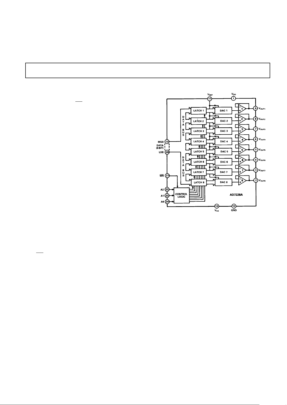
FUNCTIONAL BLOCK DIAGRAM
PRODUCT HIGHLIGHTS
1. Eight DACs and Amplifiers in Small Package
The single-chip design of eight 8-bit DACs and amplifiers allows a dramatic reduction in board space requirements and
offers increased reliability in systems using multiple converters. Its pinout is aimed at optimizing board layout with all
analog inputs and outputs at one side of the package and all
digital inputs at the other.
2. Single or Dual Supply Operation
The voltage-mode configuration of the DACs allows single
supply operation of the AD7228A. The part can also be operated with dual supplies giving enhanced performance for
some parameters.
3. Microprocessor Compatibility
The AD7228A has a common 8-bit data bus with individual
DAC latches, providing a versatile control architecture for
simple interface to microprocessors. All latch enable signals
are level triggered and speed compatible with most high performance 8-bit microprocessors.
FEATURES
Eight 8-Bit DACs with Output Amplifiers
Operates with Single +5 V, +12 V or +15 V
or Dual Supplies
mP Compatible (95 ns
WR Pulse)
No User Trims Required
Skinny 24-Pin DlPs, SOIC, and 28-Terminal Surface
Mount Packages
GENERAL DESCRIPTION
The AD7228A contains eight 8-bit voltage-mode digital-toanalog converters, with output buffer amplifiers and interface
logic on a single monolithic chip. No external trims are required
to achieve full specified performance for the part.
Separate on-chip latches are provided for each of the eight D/A
converters. Data is transferred into the data latches through a
common 8-bit TTL/CMOS (5 V) compatible input port. Address inputs A0, A1 and A2 determine which latch is loaded
when
WR goes low. The control logic is speed compatible with
most 8-bit microprocessors.
Specified performance is guaranteed for input reference voltages
from +2 to +10 V when using dual supplies. The part is also
specified for single supply +15 V operation using a reference of
+10 V and single supply +5 V operation using a reference of
+1.23 V. Each output buffer amplifier is capable of developing
+10 V across a 2 kΩ load.
The AD7228A is fabricated on an all ion-implanted, highspeed, Linear Compatible CMOS (LC
2
MOS) process which has
been specifically developed to integrate high-speed digital logic
circuits and precision analog circuits on the same chip.
REV. A
–2–
AD7228A–SPECIFICA TIONS
(VDD = 10.8 V to 16.5 V; VSS = –5 V 6 10%; GND = 0 V; V
REF
= +2 V to +10 V1; RL = 2 kΩ, CL = 100 pF unless otherwise
noted.) All specifications T
MIN
to T
MAX
unless otherwise noted.
5
Sample tested at 25°C to ensure compliance.
6
The glitch impulse transferred to the output of one converter (not addressed) due to a
change in the digital input code to another addressed converter.
Specifications subject to change without notice.
(VDD = +15 V 6 10%, VSS; = GND = 0 V; V
REF
= +10 V, RL = 2 kΩ, CL = 100 pF unless otherwise noted.)
AII specifications T
MIN
to T
MAX
unless otherwise noted.
DUAL SUPPLY
BCTU
Parameter Version2Version Version Version Units Conditions/Comments
STATIC PERFORMANCE
Resolution 8 8 8 8 Bits
Total Unadjusted Error
3
±2 ±1 ±2 ±1 LSB max VDD = +15 V ± 10%, V
REF
= +10 V
Relative Accuracy ± 1 ± 1/2 ± 1 ±1/2 LSB max
Differential Nonlinearity ± 1 ±1 ±1 ±1 LSB max Guaranteed Monotonic
Full-Scale Error
4
± 1 ± 1/2 ± 1 ± 1/2 LSB max Typical tempco is 5 ppm/°C with V
REF
= +10 V
Zero Code Error
@ 25°C ±25 ±15 ±25 ±15 mV max Typical tempco is 30 µV/°C
T
MIN
to T
MAX
±30 ±20 ±30 ±20 mV max
Minimum Load Resistance 2 2 2 2 kΩ min V
OUT
= +10 V
REFERENCE INPUT
Voltage Range
1
2 to 10 2 to 10 2 to 10 2 to 10 V min/V max
Input Resistance 2 2 2 2 kΩ min
Input Capacitance
5
500 500 500 500 pF max Occurs when each DAC is loaded with all 1s.
AC Feedthrough –70 –70 –70 –7 0 dB typ V
REF
= 8 V p-p Sine Wave @ 10 kHz
DIGITAL INPUTS
Input High Voltage, V
INH
2.4 2.4 2.4 2.4 V min
Input Low Voltage, V
INL
0.8 0.8 0.8 0.8 V max
Input Leakage Current ±1 ±1 ±1 ±1 µA max VIN = 0 V or V
DD
Input Capacitance
5
8 8 8 8 pF max
Input Coding Binary Binary Binary Binary
DYNAMIC PERFORMANCE
5
Voltage Output Slew Rate 2 2 2 2 V/µs min
Voltage Output Settling Time
Positive Full-Scale Change 5 5 5 5 µs max V
REF
= +10 V; Settling Time to ±1/2 LSB
Negative Full-Scale Change 5 5 5 5 µs max V
REF
= +10 V; Settling Time to ±1/2 LSB
Digital Feedthrough 50 50 50 50 nV secs typ Code transition all 0s to all 1s. V
REF
= 0 V; WR = V
DD
Digital Crosstalk
6
50 50 50 50 nV secs typ Code transition all 0s to all 1s. V
REF
= +10 V; WR = 0 V
POWER SUPPLIES
VDD Range 10.8/16.5 10.8/16.5 10.8/16.5 10.8/16.5 V min/V max For Specified Performance
VSS Range –4.5/–5.5 –4.5/–5.5 –4.5/–5.5 –4.5/–5.5 V min/V max For Specified Performance
I
DD
Outputs Unloaded; VIN = V
INL
or V
INH
@ 25°C 16 16 16 1 6 mA max
T
MIN
to T
MAX
20 20 22 22 mA max
I
SS
Outputs Unloaded; VIN = V
INL
or V
INH
@ 25°C 14 14 14 1 4 mA max
T
MIN
to T
MAX
18 18 20 20 mA max
SINGLE SUPPLY
STATIC PERFORMANCE
Resolution 8 8 8 8 Bits
Total Unadjusted Error
3
±2 ±1 ±2 ±1 LSB max
Differential Nonlinearity ± 1 ±1 ±1 ±1 LSB max Guaranteed Monotonic
Minimum Load Resistance 2 2 2 2 kΩ min V
OUT
= +10 V
REFERENCE INPUT
Input Resistance 2 2 2 2 kΩ min
Input Capacitance
5
500 500 500 500 pF max Occurs when each DAC is loaded with all 1s.
DIGITAL INPUTS As per Dual Supply Specifications
DYNAMIC PERFORMANCE
5
Voltage Output Slew Rate 2 2 2 2 V/µs min
Voltage Output Settling Time
Positive Full-Scale Change 5 5 5 5 µs max Settling Time to ±1/2 LSB
Negative Full-Scale Change 7 7 7 7 µs max Settling Time to ±1/2 LSB
Digital Feedthrough 50 50 50 50 nV secs typ Code transition all 0s to all 1s. V
REF
= 0 V; WR = V
DD
Digital Crosstalk
6
50 50 50 50 nV secs typ Code transition all 0s to all 1s. V
REF
= +10 V, WR = 0 V
POWER SUPPLIES
VDD Range 13.5/16.5 13.5/16.5 13.5/16.5 13.5/16.5 V min/V max For Specified Performance
I
DD
Outputs Unloaded; VIN = V
INL
or V
INH
@ 25°C 16 16 16 1 6 mA max
T
MIN
to T
MAX
20 20 22 22 mA max
NOTES
1
V
OUT
must be less than VDD by 3.5 V to ensure correct operation.
2
Temperature ranges are as follows:
B, C Versions; –40°C to +85°C
T, U Versions; –55°C to +125°C
3
Total Unadjusted Error includes zero code error, relative accuracy and full-scale error.
4
Calculated after zero code error has been adjusted out.
SWITCHING CHARACTERISTICS
1, 2
Limit at 25°C Limit at T
MIN
, T
MAX
Limit at T
MIN
, T
MAX
Parameters All Grades (B, C Versions) (T, U Versions) Units Conditions/Comments
t
1
0 0 0 ns min Address to WR Setup Time
t
2
0 0 0 ns min Address to WR Hold Time
t
3
70 90 100 ns min Data Valid to WR Setup Time
t
4
10 10 10 ns min Data Valid to WR Hold Time
t
5
95 120 150 ns min Write Pulse Width
NOTES
1
Sample tested at 25°C to ensure compliance. All input rise and fall times measured from 10% to 90% of +5 V, tR = tF = 5 ns.
2
Timing measurement reference level is
V
INH+VINL
2
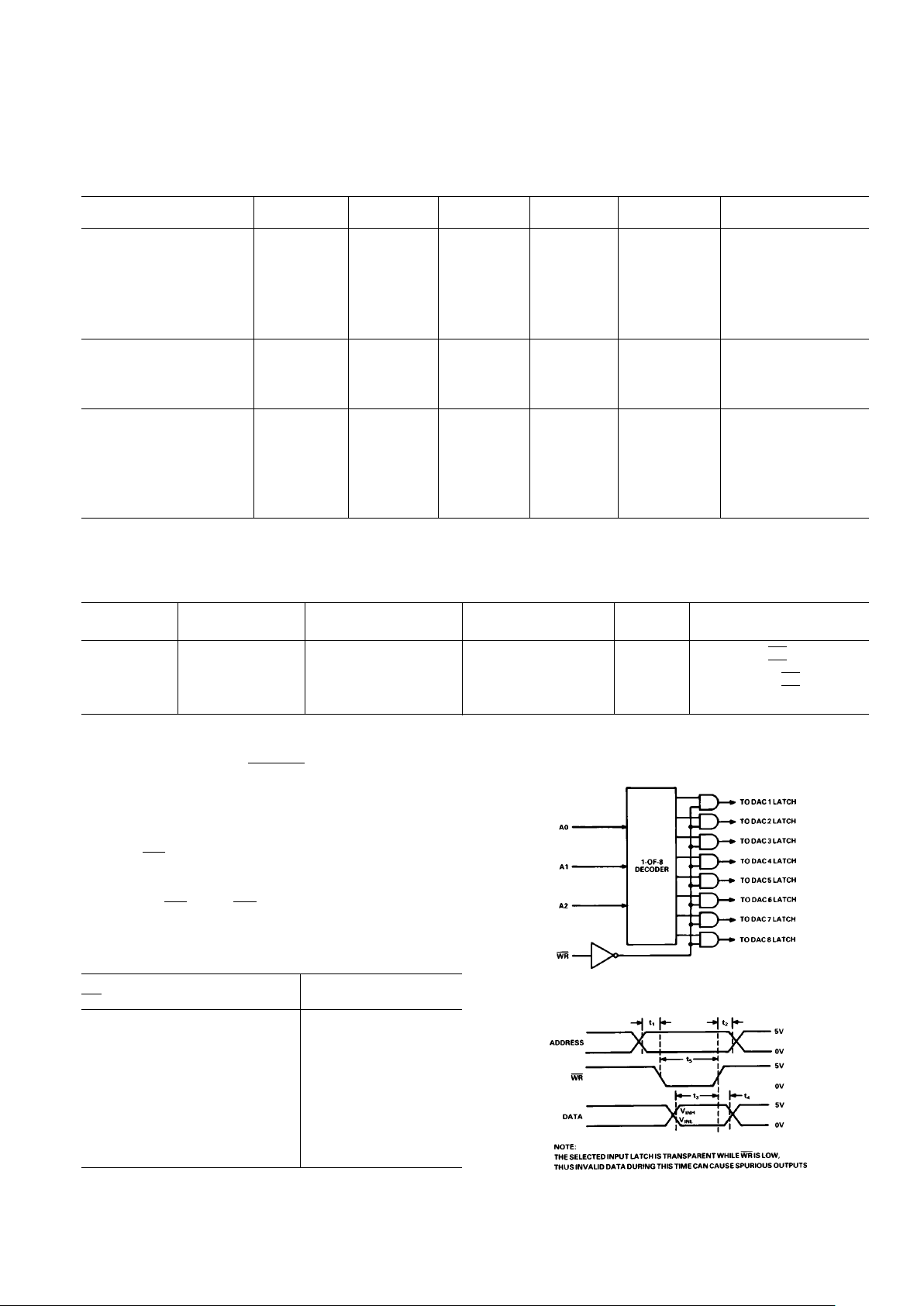
INTERFACE LOGIC INFORMATION
Address lines A0, A1 and A2 select which DAC accepts data
from the input port. Table I shows the selection table for the
eight DACs with Figure 1 showing the input control logic.
When the
WR signal is low, the input latch of the selected DAC
is transparent, and its output responds to activity on the data
bus. The data is latched into the addressed DAC latch on the
rising edge of
WR. While WR is high, the analog outputs remain
at the value corresponding to the data held in their respective
latches.
Table I. AD7228A Truth Table
AD7228A Control Inputs AD7228A
WR A2 A1 A0 Operation
H X X X No Operation
Device Not Selected
LLLL DAC 1 Transparent
g
L L L DAC 1 Latched
LLLH DAC 2 Transparent
L L H L DAC 3 Transparent
L L H H DAC 4 Transparent
L H L L DAC 5 Transparent
L H L H DAC 6 Transparent
L H H L DAC 7 Transparent
L H H H DAC 8 Transparent
H = High State L = Low State X = Don’t Care
+5 V SUPPLY OPERA TION
BCTU
Parameter Version Version Version Version Units Conditions/Comments
STATIC PERFORMANCE
Resolution 8888Bits
Relative Accuracy ± 2 ±2 ±2 ±2 LSB max
Differential Nonlinearity ±1 ±1 ±1 ±1 LSB max Guaranteed Monotonic
Full-Scale Error ± 4 ±2 ±4 ±2 LSB max
Zero Code Error
@ 25°C ±30 ±20 ± 30 ±20 mV max
T
MIN
to T
MAX
±40 ± 30 ±40 ±30 mV max
REFERENCE INPUT
Reference Input Range 1.2 1.2 1.2 1.2 V min
1.3 1.3 1.3 1.3 V max
Reference Input Resistance 2222kΩ min
Reference Input Capacitance 500 500 500 500 pF max
POWER REQUIREMENTS
Positive Supply Range 4.75/5.25 4.75/5.25 4.75/5.25 4.75/5.25 V min/V max For Specified Performance
Positive Supply Current
@ 25°C 16161616µA max
T
MIN
to T
MAX
20 20 22 22 µA max
Negative Supply Current
@ 25°C 14141414µA max
T
MIN
to T
MAX
18 18 20 20 µA max
NOTES
All of the specifications as per Dual Supply Specifications except for negative full-scale settling-time when V
SS
= 0 V.
Specifications subject to change without notice.
(VDD = +5 V 6 5%, VSS; = 0 to –5 V 6 10%, GND = 0 V, V
REF
= +1.25 V, RL = 2 kV, CL = 100 pF
unless otherwise noted.) AII specifications T
MIN
to T
MAX
unless otherwise noted.
(See Figures 1, 2; VDD = +5 V 6 5% or +10.8 V to +16.5 V; VSS = 0 V or –5 V 6 10%)
Figure 1. Input Control Logic
Figure 2. Write Cycle Timing Diagram
AD7228A
REV. A
–3–

AD7228A
REV. A
–4–
ABSOLUTE MAXIMUM RATINGS
1
VDD to GND . . . . . . . . . . . . . . . . . . . . . . . . . . .–0.3 V, +17 V
V
DD
to VSS . . . . . . . . . . . . . . . . . . . . . . . . . . . . .–0.3 V, +24 V
Digital Input Voltage to GND . . . . . . . . . . . . . . . –0.3 V, V
DD
V
REF
to GND . . . . . . . . . . . . . . . . . . . . . . . . . . . . . –0.3V, V
DD
V
OUT
to GND2 . . . . . . . . . . . . . . . . . . . . . . . . . . . . . . VSS, V
DD
Power Dissipation (Any Package) to +75°C . . . . . . . 1000 mW
Derates above 75°C by . . . . . . . . . . . . . . . . . . . . 2.0 mW/°C
Operating Temperature
Commercial . . . . . . . . . . . . . . . . . . . . . . . . –40°C to +85°C
Industrial . . . . . . . . . . . . . . . . . . . . . . . . . . –40°C to +85°C
Extended . . . . . . . . . . . . . . . . . . . . . . . . . –55°C to +125°C
Storage Temperature . . . . . . . . . . . . . . . . . . –65°C to +150°C
Lead Temperature (Soldering, 10 secs) . . . . . . . . . . . +300°C
NOTES
1
Stresses above those listed under “Absolute Maximum Ratings” may cause
permanent damage to the device. This is a stress rating only and functional
operation of the device at these or any other conditions above those indicated in the
operational sections of this specification is not implied. Exposure to absolute
maximum rating conditions for extended periods may affect device reliability.
2
Outputs may be shorted to any voltage in the range VSS to VDD provided that the
power dissipation of the package is not exceeded. Typical short circuit current for
a short to GND or VSS is 50 mA.
WARNING!
ESD SENSITIVE DEVICE
CAUTION
ESD (electrostatic discharge) sensitive device. Electrostatic charges as high as 4000 V readily
accumulate on the human body and test equipment and can discharge without detection.
Although the AD7228A features proprietary ESD protection circuitry, permanent damage may
occur on devices subjected to high energy electrostatic discharges. Therefore, proper ESD
precautions are recommended to avoid performance degradation or loss of functionality.
PIN CONFIGURATIONS
DIP AND SOIC PLCC
ORDERING GUIDE
Total
Temperature Unadjusted Package
Model
1
Range Error (LSB) Option
2
AD7228ABN –40°C to +85°C ±2 max N-24
AD7228ACN –40°C to +85°C ±1 max N-24
AD7228ABP –40°C to +85°C ±2 max P-28A
AD7228ACP –40°C to +85°C ±1 max P-28A
AD7228ABR –40°C to +85°C ±2 max R-24
AD7228ACR –40°C to +85°C ±1 max R-24
AD7228ABQ –40°C to +85°C ±2 max Q-24
AD7228ACQ –40°C to +85°C ±1 max Q-24
AD7228ATQ
3
–55°C to +125°C ±2 max Q-24
AD7228AUQ3–55°C to +125°C ±1 max Q-24
NOTES
1
To order MIL-STD-883, Class B processed parts, add /883B to part number.
Contact your local sales office for military data sheet and availability.
2
N = Plastic DIP; P = Plastic Leaded Chip Carrier (PLCC); Q = Cerdip;
R = Small Outline IC (SOIC).
3
These grades will be available to /883B processing only.
CIRCUIT INFORMATION
D/A SECTION
The AD7228A contains eight identical, 8-bit, voltage-mode
digital-to-analog converters. The output voltages from the converters have the same polarity as the reference voltage, allowing
single supply operation. A novel DAC switch pair arrangement
on the AD7228A allows a reference voltage range from +2 V to
+10 V when operated from a V
DD
of +15 V. Each DAC consists
of a highly stable, thin-film, R-2R ladder and eight high-speed
NMOS switches. The simplified circuit diagram for one channel
is shown in Figure 3. Note that V
REF
and GND are common to
all eight DACs.
Figure 3. D/A Simplified Circuit Diagram
The input impedance at the V
REF
pin of the AD7228A is the
parallel combination of the eight individual DAC reference input impedances. It is code dependent and can vary from 2 kΩ to
infinity. The lowest input impedance occurs when all eight
DACs are loaded with digital code 01010101. Therefore, it is
important that the external reference source presents a low output impedance to the V
REF
terminal of the AD7228A under
changing load conditions. Due to transient currents at the reference input during digital code changes a 0.1 µF (or greater)
decoupling capacitor is recommended on the V
REF
input for dc
applications. The nodal capacitance at the reference terminal is
also code dependent and typically varies from 120 pF to
350 pF.
Each V
OUT
pin can be considered as a digitally programmable
voltage source with an output voltage:
V
OUTN
= DN • V
REF
where DN is a fractional representation of the digital input
code and can vary from 0 to 255/256.
The output impedance is that of the output buffer amplifier as
described in the following section.

AD7228A
REV. A
–5–
OP AMP SECTION
Each voltage-mode D/A converter output is buffered by a unity
gain noninverting CMOS amplifier. This buffer amplifier is
tested with a 2 kΩ and 100 pF load but will typically drive a
2 kΩ and 500 pF load.
The AD7228A can be operated single or dual supply. Operating
the part from single or dual supplies has no effect on the positivegoing settling time. However, the negative-going settling time to
voltages near 0 V in single supply will be slightly longer than the
settling time for dual supply operation. Additionally, to ensure
that the output voltage can go to 0 V in single supply, a transistor on the output acts as a passive pull-down as the output voltage nears 0 V. As a result, the sink capability of the amplifier is
reduced as the output voltage nears 0 V in single supply. In dual
supply operation, the full sink capability of 400 µA at 25°C is
maintained over the entire output voltage range. The single supply output sink capability is shown in Figure 4. The negative
V
SS
also gives improved output amplifier performance allowing
an extended input reference voltage range and giving improved
slew rate at the output.
Figure 4. Single Supply Sink Current
The output broadband noise from the amplifier is 300 µV
peak-to-peak. Figure 5 shows a plot of noise spectral density
versus frequency.
Figure 5. Noise Spectral Density vs. Frequency
DIGITAL INPUTS
The AD7228A digital inputs are compatible with either TTL or
5 V CMOS levels. All logic inputs are static-protected MOS
gates with typical input currents of less than 1 nA. Internal input protection is achieved by on-chip distributed diodes.
SUPPLY CURRENT
The AD7228A has a maximum IDD specification of 22 mA and
a maximum I
SS
of 20 mA over the –55°C to +125°C temperature range. This maximum current specification is actually determined by the current at –55°C. Figure 6 shows a typical plot
of power supply current versus temperature.
Figure 6. Power Supply Current vs. Temperature
APPLYING THIS AD7228A
UNIPOLAR OUTPUT OPERATION
This is the basic mode of operation for each channel of the
AD7228A, with the output voltage having the same positive polarity as V
REF
. Connections for unipolar output operation are
shown in Figure 7. The AD7228A can be operated from single
or dual supplies as outlined earlier. The voltage at the reference
input must never be negative with respect to GND. Failure to
observe this precaution may cause parasitic transistor action and
possible device destruction. The code table for unipolar output
operation is shown in Table II.
Figure 7. Unipolar Output Circuit

AD7228A
REV. A
–6–
Table II. Unipolar Code Table
DAC Latch Contents
MSB LSB Analog Output
1 1 1 1 1 1 1 1
+V
REF
255
256
1 0 0 0 0 0 0 1
+V
REF
129
256
1 0 0 0 0 0 0 0
+V
REF
128
256
=+
V
REF
2
0 1 1 1 1 1 1 1
+V
REF
127
256
0 0 0 0 0 0 0 1
+V
REF
1
256
0 0 0 0 0 0 0 0 0 V
Note: 1 LSB = (V
REF
)(2–8) = V
REF
1
256
BIPOLAR OUTPUT OPERATION
Each of the DACs on the AD7228A can be individually configured for bipolar output operation. This is possible using one external amplifier and two resistors per channel. Figure 8 shows a
circuit used to implement offset binary coding (bipolar operation) with DAC1 of the AD7228A. In this case
V
OUT
= 1+
R2
R1
• D
1•VREF
()
–
R2
R1
•V
REF
()
With R1 = R2
V
OUT
= (2D1 – 1) • (V
REF
)
where D
1
is a fractional representation of the digital word in
latch 1 of the AD7228A. (0 ≤ D
1
≤ 255/256)
Figure 8. Bipolar Output Circuit
Table III. Bipolar Code Table
DAC Latch Contents
MSB LSB Analog Output
1 1 1 1 1 1 1 1
+V
REF
127
128
1 0 0 0 0 0 0 1
+V
REF
1
128
1 0 0 0 0 0 0 0 0 V
0 1 1 1 1 1 1 1
–V
REF
1
128
0 0 0 0 0 0 0 1
–V
REF
127
128
0 0 0 0 0 0 0 0
–V
REF
128
128
= –V
REF
Mismatch between R1 and R2 causes gain and offset errors, and
therefore, these resistors must match and track over temperature.
Once again, the AD7228A can be operated from single supply
or from dual supplies. Table III shows the digital code versus
output voltage relationship for the circuit of Figure 8 with
R1 = R2.
AC REFERENCE SIGNAL
In some applications it may be desirable to have an ac signal applied as the reference input to the AD7228A. The AD7228A
has multiplying capability within the upper (+10 V) and lower
(+2 V) limits of reference voltage when operated with dual supplies. Therefore, ac signals need to be ac coupled and biased up
before being applied to the reference input. Figure 9 shows a
sine-wave signal applied to the reference input of the AD7228A.
For input frequencies up to 50 kHz, the output distortion typically remains less than 0.1%. The typical 3 dB bandwidth for
small signal inputs is 800 kHz.
Figure 9. Applying a AC Signal to the AD7228A
TIMING DESKEW
A common problem in ATE applications is the slowing or
“rounding-off” of signal edges by the time they reach the
pin-driver circuitry. This problem can easily be overcome by
“squaring-up” the edge at the pin-driver. However, since each
edge will not have been “rounded-off” by the same extent, this
“squaring-up” could lead to incorrect timing relationship between signals. This effect is shown in Figure 10a.
Figure 10a. Time Skewing Due to Slowing of Edges
The circuit of Figure 10b shows how two DACs of the
AD7228A can help in overcoming this problem. The same two
signals are applied to this circuit as were applied in Figure 10b.
The output of each DAC is applied to one input of a high-speed
comparator, and the signals are applied to the other inputs.
Varying the output voltage of the DAC effectively varies the
trigger point at which the comparator flips. Thus the timing relationship between the two signals can be programmably corrected (or deskewed) by varying the code to the DAC of the
AD7228A. In a typical application, the code is loaded to the

AD7228A
REV. A
–7–
DACs for correct timing relationships during the calibration
cycle of the instrument.
Figure 10b. AD7228A Timing Deskew Circuit
COARSE/FINE ADJUST
The DACs on the AD7228A can be paired together to form a
coarse/fine adjust function as indicated in Figure 11. The function is achieved using one external op amp and a few resistors
per pair of DACs.
DAC1 is the most significant or coarse DAC. Data is first
loaded to this DAC to coarsely set the output voltage. DAC2 is
then used to fine tune this output voltage. Varying the ratio of
R1 to R2 varies the relative effect of the coarse and fine DACs
on the output voltage. For the resistor values shown, DAC2 has
a resolution of 150 µV in a 10 V output range. Since each DAC
on the AD7228A is guaranteed monotonic, the coarse adjustment and fine adjustment are each monotonic. One application
for this is as a set-point controller (see “Circuit Applications of
the AD7226 Quad CMOS DAC” available from Analog Devices,
Publication Number E873–15–11/84).
Figure 11. Coarse/Fine Adjust Circuit
SELF-PROGRAMMABLE REFERENCE
The circuit of Figure 12 shows how one DAC of the AD7228,
in this case DAC1, may be used in a feedback configuration to
provide a programmable reference for itself and the other seven
converters. The relationship of V
REF
to VIN is expressed by
V
REF
=
1+G
()
1+G•D
1
()
•V
IN
where G = R2/R1
Figure 13 shows typical plots of V
REF
versus digital code, D1, for
three different values of G. With V
IN
= 2.5 V and G = 3 the
voltage at the output varies between 2.5 V and 10 V giving an
effective 10-bit dynamic range to the other seven converters. For
correct operation of the circuit, V
SS
should be –5 V and R1
greater than 6.8 kΩ.
Figure 12. Self-Programmable Reference
Figure 13. Variation of V
REF
with Feedback Configuration
MICROPROCESSOR INTERFACING
Figure 14. AD7228A to 8085A/Z80 Interface
Figure 15. AD7228A to 6809/6502 Interface

AD7228A
REV. A
–8–
C1663–24–5/92
PRINTED IN U.S.A.
Figure 16. AD7228A to 68008 Interface
Plastic DIP (N-24)
SOIC (R-24)
Cerdip (Q-24)
PLCC (P-28A)
Figure 17. AD7228A to MCS-51 Interface
OUTLINE DIMENSIONS
Dimensions shown in inches and (mm).
 Loading...