

Quad Picoampere Input Current
2
3
11
10
12
13
14
15
16
9
1
2
3
4
5
6
7
8
NC = NO CONNECT
NC
1
4
OUTPUT
–IN
–IN
OUTPUT
OUTPUT
–IN
–IN
OUTPUT
AD704
(TOP VIEW)
+IN
+IN
+IN
+V
S
–V
S
+IN
NC
a
FEATURES
High DC Precision
75 V Max Offset Voltage
1 V/ⴗC Max Offset Voltage Drift
150 pA Max Input Bias Current
0.2 pA/ⴗC Typical I
Drift
B
Low Noise
0.5 V p-p Typical Noise, 0.1 Hz to 10 Hz
Low Power
600 A Max Supply Current per Amplifier
MIL-STD-883B Processing Available
Available in Tape and Reel in Accordance
with EIA-481A Standard
Dual Version: AD706
APPLICATIONS
Industrial/Process Controls
Weigh Scales
ECG/EKG Instrumentation
Low Frequency Active Filters
PRODUCT DESCRIPTION
The AD704 is a quad, low power bipolar op amp that has the
low input bias current of a BiFET amplifier but which offers a
significantly lower I
drift over temperature. It utilizes super-beta
B
bipolar input transistors to achieve picoampere input bias current
levels (similar to FET input amplifiers at room temperature),
while its I
BiFET amp, for which I
typically only increases by 5× at 125°C (unlike a
B
doubles every 10°C resulting in a
B
1000× increase at 125°C). Furthermore, the AD704 achieves
75 µV offset voltage and low noise characteristics of a precision
bipolar input op amp.
Since it has only 1/20 the input bias current of an AD OP07, the
AD704 does not require the commonly used “balancing” resistor.
Furthermore, the current noise is 1/5 that of the AD OP07 which
makes the AD704 usable with much higher source impedances.
At 1/6 the supply current (per amplifier) of the AD OP07, the
AD704 is better suited for today’s higher density circuit boards
and battery-powered applications.
The AD704 is an excellent choice for use in low frequency active
filters in 12- and 14-bit data acquisition systems, in precision
instrumentation, and as a high quality integrator. The AD704 is
internally compensated for unity gain and is available in five
performance grades. The AD704J and AD704K are rated over
the commercial temperature range of 0°C to 70°C. The AD704A
is rated over the industrial temperature of –40°C to +85°C. The
AD704T is rated over the military temperature range of –55°C
to +125°C and is available processed to MIL-STD-883B, Rev. C.
REV. C
Information furnished by Analog Devices is believed to be accurate and
reliable. However, no responsibility is assumed by Analog Devices for its
use, nor for any infringements of patents or other rights of third parties that
may result from its use. No license is granted by implication or otherwise
under any patent or patent rights of Analog Devices.
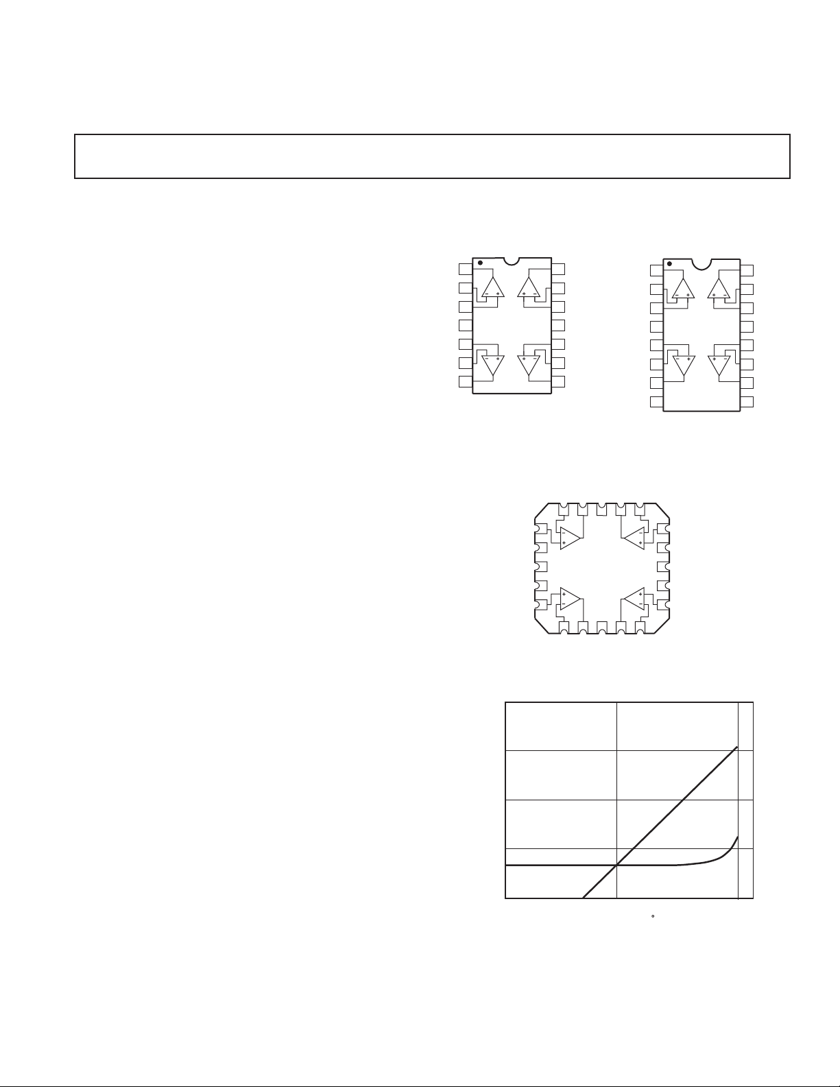
14-Lead CerDIP (Q) Packages
OUTPUT
OUTPUT
Bipolar Op Amp
AD704
CONNECTION DIAGRAMS
14-Lead Plastic DIP (N)
14
OUTPUT
13
4
3
–IN
12
+IN
11
–V
10
9
8
S
+IN
–IN
OUTPUT
)
+V
–IN
+IN
+IN
–IN
1
2
1
3
AD704
4
S
5
6
7
(TOP VIEW
2
20-Terminal LCC
(E) Package
–IN1
OUT1
3212019
4
+IN1
5
NC
+V
6
S
7
NC
8
+IN2
910111213
100
10
– nA
B
1
TYPICAL I
0.1
0.01
–55 +25 +125
NC
AMP 1
AD704
AMP 2
–IN2
OUT2NCOUT3
TEMPERATURE – C
Figure 1. Input Bias Current Over Temperature
One Technology Way, P.O. Box 9106, Norwood, MA 02062-9106, U.S.A.
Tel: 781/329-4700www.analog.com
Fax: 781/326-8703 © Analog Devices, Inc., 2002
16-Lead SOIC
(R) Package
–IN4
OUT4
18
AMP 4
AMP 3
TYPICAL JFET AMP
17
16
15
14
–IN3
NC = NO CONNECT
AD704T
+IN4
NC
–V
NC
+IN3
S

AD704–SPECIFICATIONS
(@ TA = 25ⴗC, VCM = 0 V, and ⴞ15 V dc, unless otherwise noted.)
AD704J/A AD704K AD704T
Parameters Conditions Min Typ Max Min Typ Max Min Typ Max Unit
INPUT OFFSET VOLTAGE
Initial Offset 50 150 30 75 30 100 µV
Offset T
MIN–TMAX
100 250 50 150 80 150 µV
vs. Temp, Average TC 0.2 1.5 0.2 1.0 1.0 µV/°C
vs. Supply (PSRR) VS = ±2 to ± 18 V 100 132 112 132 112 132 dB
T
MIN–TMAX
VS = ±2.5 to ± 18 V 100 126 108 126 108 126 dB
Long-Term Stability 0.3 0.3 0.3 µV/month
INPUT BIAS CURRENT
1
VCM = 0 V 100 270 80 150 80 200 pA
= ±13.5 V 300 200 250 pA
V
CM
vs. Temp, Average TC 0.3 0.2 1.0 pA/°C
T
MIN–TMAX
VCM = 0 V 300 200 600 pA
VCM = ±13.5 V 400 300 700 pA
INPUT OFFSET CURRENT V
= 0 V 80 250 30 100 50 150 pA
CM
= ±13.5 V 300 150 200 pA
V
CM
vs. Temp, Average TC 0.6 0.4 0.4 pA/°C
T
MIN–TMAX
VCM = 0 V 100 300 80 200 80 400 pA
VCM = ±13.5 V 100 400 80 300 100 500 pA
MATCHING CHARACTERISTICS
Offset Voltage 250 130 150 µV
Input Bias Current
2
Common-Mode Rejection
Power Supply Rejection
Crosstalk
5
4
T
MIN–TMAX
T
3
MIN–TMAX
T
MIN–TMAX
94 110 104 dB
94 104 104 dB
94 110 110 dB
T
MIN–TMAX
94 106 106 dB
f = 10 Hz
R
= 2 kΩ 150 150 150 dB
LOAD
400 200 250 µV
500 300 400 pA
600 400 600 pA
FREQUENCY RESPONSE
UNITY GAIN
Crossover Frequency 0.8 0.8 0.8 MHz
Slew Rate, Unity Gain G = –1 0.15 0.15 0.15 V/µs
Slew Rate T
MIN–TMAX
0.1 0.1 0.1 V/µs
INPUT IMPEDANCE
Differential 40储240储240储2MΩ储pF
Common-Mode 300储2 300储2 300储2GΩ储pF
INPUT VOLTAGE RANGE
Common-Mode Voltage ±13.5 ± 14 ±13.5 ±14 ±13.5 ± 14 V
Common-Mode Rejection Ratio V
= ±13.5 V 100 132 114 132 110 132 dB
CM
T
MIN–TMAX
98 128 108 128 108 128 dB
INPUT CURRENT NOISE 0.1 to 10 Hz 3 3 3 pA p-p
f = 10 Hz 50 50 50 fA/√Hz
INPUT VOLTAGE NOISE 0.1 to 10 Hz 0.5 0.5 2.0 0.5 2.0 µV p-p
f = 10 Hz 17 17 17 nV/√Hz
f = 1 kHz 15 22 15 22 15 22 nV/√Hz
OPEN-LOOP GAIN V
= ±12 V
O
= 10 kΩ 200 2000 400 2000 400 2000 V/mV
R
LOAD
T
MIN–TMAX
= ±10 V
V
O
= 2 kΩ 200 1000 300 1000 200 1000 V/mV
R
LOAD
T
MIN–TMAX
150 1500 300 1500 300 1500 V/mV
150 1000 200 1000 100 1000 V/mV
–2–
REV. C

AD704
Parameters Conditions Min Typ Max Min Typ Max Min Typ Max Unit
AD704J/A AD704K AD704T
OUTPUT CHARACTERISTICS
Voltage Swing R
= 10 kΩ
LOAD
T
MIN–TMAX
±13 ±14 ± 13 ±14 ±13 ±14 V
Current Short Circuit ±15 ±15 ±15 mA
CAPACITIVE LOAD
Drive Capability Gain = 1 10,000 10,000 10,000 pF
POWER SUPPLY
Rated Performance ±15 ±15 ±15 V
Operating Range ±2.0 ±18 ±2.0 ±18 ±2.0 ±18 V
Quiescent Current 1.5 2.4 1.5 2.4 1.5 2.4 mA
T
MIN–TMAX
1.6 2.6 1.6 2.6 1.6 2.6 mA
TRANSISTOR COUNT # of Transistors 180 180 180
NOTES
1
Bias current specifications are guaranteed maximum at either input.
2
Input bias current match is the maximum difference between corresponding inputs of all four amplifiers.
3
CMRR match is the difference of ∆VOS/∆VCM between any two amplifiers, expressed in dB.
4
PSRR match is the difference between ∆VOS/∆V
5
See Figure 2a for test circuit.
All min and max specifications are guaranteed.
Specifications subject to change without notice.
for any two amplifiers, expressed in dB.
SUPPLY
REV. C
–3–
AD704
1/4
AD704
OUTPUT
INPUT*
SIGNAL
9k⍀
1k⍀
1k⍀
2.5k⍀
–
+
ALL 4 AMPLIFIERS ARE CONNECTED AS SHOWN
*THE SIGNAL INPUT (SUCH THAT THE AMPLIFIER’S OUTPUT IS AT MAX
AMPLITUDE WITHOUT CLIPPING OR SLEW LIMITING) IS APPLIED TO ONE
AMPLIFIER AT A TIME. THE OUTPUTS OF THE OTHER THREE AMPLIFIERS
ARE THEN MEASURED FOR CROSSTALK.
AD704
PIN 4
AD704
PIN 11
COM
0.1F
1F
0.1F
1F
+V
S
–V
S
WARNING!
ESD SENSITIVE DEVICE
ABSOLUTE MAXIMUM RATINGS
1
Supply Voltage . . . . . . . . . . . . . . . . . . . . . . . . . . . . . . . . ± 18 V
Internal Power Dissipation (25°C) . . . . . . . . . . . . See Note 2
Input Voltage . . . . . . . . . . . . . . . . . . . . . . . . . . . . . . . . . . . ± V
S
Differential Input Voltage3 . . . . . . . . . . . . . . . . . . . . . . . ± 0.7 V
Output Short-Circuit Duration (Single Input) . . . . . Indefinite
Storage Temperature Range
Q . . . . . . . . . . . . . . . . . . . . . . . . . . . . . . . –65°C to +150°C
N, R . . . . . . . . . . . . . . . . . . . . . . . . . . . . . –65°C to +125°C
Operating Temperature Range
AD704J/K . . . . . . . . . . . . . . . . . . . . . . . . . . . . 0°C to 70°C
AD704A . . . . . . . . . . . . . . . . . . . . . . . . . . . –40°C to +85°C
AD704T . . . . . . . . . . . . . . . . . . . . . . . . . –55°C to +125°C
Lead Temperature Range (Soldering 10 seconds) . . . . . 300°C
NOTES
1
Stresses above those listed under Absolute Maximum Ratings may cause perma-
nent damage to the device. This is a stress rating only; functional operation of the
device at these or any other conditions above those indicated in
the operational section of this specification is not implied. Exposure to absolute
maximum rating conditions for extended periods may affect device reliability.
2
Specification is for device in free air:
14-Lead Plastic Package: θJA = 150°C/W
14-Lead Cerdip Package: θJA = 110°C/W
16-Lead SOIC Package: θJA = 100°C/W
20-Terminal LCC Package: θJA = 150°C/W
3
The input pins of this amplifier are protected by back-to-back diodes. If the
differential voltage exceeds ± 0.7 volts, external series protection resistors should
be added to limit the input current to less than 25 mA.
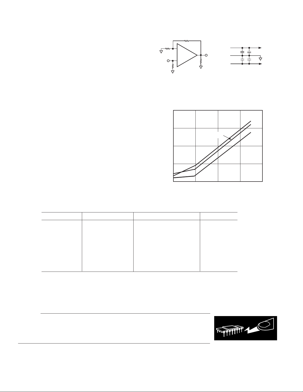
Figure 2a. Crosstalk Test Circuit
–80
–100
AMP2
–120
CROSSTALK – dB
–140
–160
10 100 1k 10k 100k
FREQUENCY – Hz
Figure 2b. Crosstalk vs. Frequency
AMP4
AMP3
ORDERING GUIDE
Model Temperature Range Package Description Package Option
AD704JN 0°C to 70°C Plastic N-14
AD704JR 0°C to 70°C Small Outline (SOIC) R-16
AD704JR-/REEL 0°C to 70°C Tape and Reel
AD704KN
AD704AN
*
*
0°C to 70°C Plastic N-14
–40°C to +85°C Plastic N-14
AD704AR –40°C to +85°C Small Outline (SOIC) R-16
AD704AR-REEL –40°C to +85°C Tape and Reel
AD704SE/883B –55°C to +125°C Leadless Ceramic Chip Carrier E-20A
AD704TQ/883B
Chips are also available.
*Not for new designs; obsolete April 2002.
*
–55°C to +125°C Cerdip Q-14
CAUTION
ESD (electrostatic discharge) sensitive device. Electrostatic charges as high as 4000 V readily
accumulate on the human body and test equipment and can discharge without detection. Although
the AD704 features proprietary ESD protection circuitry, permanent damage may occur on devices
subjected to high-energy electrostatic discharges. Therefore, proper ESD precautions are
recommended to avoid performance degradation or loss of functionality.
–4–
REV. C

(@ 25ⴗC, VS = ⴞ15 V dc, unless otherwise noted.)
100
10
1.0
0.1
1k 10k 100k 1M 10M 100M
SOURCE RESISTANCE – ⍀
SOURCE RESISTANCE
MAY BE EITHER BALANCED
OR UNBALANCED
OFFSET VOLTAGE DRIFT – V/ⴗC
50
Typical Performance Characteristics–AD704
50
50
40
30
20
PERCENTAGE OF UNITS
10
0
–80 –40 0 +40 +80
INPUT OFFSET VOLTAGE – V
TPC 1. Typical Distribution of
Input Offset Voltage
+V
S
–0.5
–1.0
–1.5
+1.5
+1.0
+0.5
(REFERRED TO SUPPLY VOLTAGES)
INPUT COMMON-MODE VOLTAGE LIMIT – V
–V
S
0 5 10 15 20
SUPPLY VOLTAGE – V
TPC 4. Input Common-Mode
Voltage Range vs. Supply Voltage
40
30
20
PERCENTAGE OF UNITS
10
0
–160 –80 0 +80 +160
INPUT BIAS CURRENT – pA
TPC 2. Typical Distribution of
Input Bias Current
35
30
25
20
15
10
OUTPUT VOLTAGE – V p-p
5
0
1k 10k 100k
FREQUENCY – Hz
TPC 5. Large Signal Frequency
Response
1M
40
30
20
PERCENTAGE OF UNITS
10
0
–120 –60 0 +60 +120
INPUT OFFSET CURRENT – pA
TPC 3. Typical Distribution of
Input Offset Current
TPC 6. Offset Voltage Drift vs.
Source Resistance
50
40
30
20
PERCENTAGE OF UNITS
10
0
–0.8 –0.4 0 +0.4 +0.8
REV. C
INPUT OFFSET VOLTAGE DRIFT – V/ⴗC
TPC 7. Typical Distribution of
Offset Voltage Drift
4
3
2
1
CHANGE IN OFFSET VOLTAGE – V
0
012345
WARM-UP TIME – Minutes
TPC 8. Change in Input Offset
Voltage vs. Warm-Up Time
–5–
120
100
80
60
40
INPUT BIAS CURRENT – pA
20
0
–15 –10 –50 51015
POSITIVE I
COMMON-MODE VOLTAGE – V
B
NEGATIVE I
B
TPC 9. Input Bias Current vs.
Common-Mode Voltage

AD704
1000
100
10
VOLTAGE NOISE – nV/ Hz
1
1 10 100
FREQUENCY – Hz
1000
TPC 10. Input Noise Voltage
Spectral Density
500
450
400
350
QUIESCENT CURRENT – A
300
0 5 10 15 20
+125
C
C
+25
C
–55
SUPPLY VOLTAGE – ⴞV
TPC 13. Quiescent Supply Current
vs. Supply Voltage (per Amplifier)
1000
100
10k⍀
100⍀
10
20M⍀
CURRENT NOISE – fA/ Hz
1
1 10 100 1000
V
OUT
FREQUENCY – Hz
TPC 11. Input Noise Current
Spectral Density
160
140
120
VS = 15V
100
80
CMR – dB
60
40
20
0
0.1 1 10 100 1k 10k 100k 1M
FREQUENCY – Hz
TPC 14. Common-Mode
Rejection vs. Frequency
0.5V
0510
TIME – Seconds
TPC 12. 0.1 Hz to 10 Hz Noise Voltage
180
VS = 15V
160
140
120
100
PSR – dB
= 25 C
T
A
80
60
40
20
0.1 1 10 100 1k 10k 100k 1M
+PSR
FREQUENCY – Hz
–PSR
TPC 15. Power Supply Rejection
vs. Frequency
10M
–55ⴗ C
+25ⴗ C
1M
OPEN-LOOP VOLTAGE GAIN
100k
1 10 100
LOAD RESISTANCE – k⍀
+125ⴗ C
TPC 16. Open-Loop Gain vs. Load
Resistance Over Temperature
140
120
100
80
60
40
20
OPEN-LOOP VOLTAGE GAIN – dB
0
–20
0.01 0.1 1 10 100 1k 10k 100k 1M 10M
FREQUENCY – Hz
PHASE
GAIN
0
30
60
90
120
150
180
TPC 17. Open-Loop Gain and Phase
vs. Frequency
–6–
+V
S
RL = 10k⍀
–0.5
–1.0
–1.5
+1.5
+1.0
PHASE SHIFT – Degrees
OUTPUT VOLTAGE SWING – V
+0.5
(REFERRED TO SUPPLY VOLTAGES)
–V
S
0 5 10 15 20
SUPPLY VOLTAGE – ⴞV
TPC 18. Output Voltage Swing vs.
Supply Voltage
REV. C

AD704
SQUARE
WAVE INPUT
0.1F
V
OUT
C
L
RL
2.5k⍀
10k⍀
10k⍀
–
+
1/4
AD704
0.1F
+V
S
–V
S
V
IN
1000
100
10
1
0.1
0.01
CLOSED-LOOP OUTPUT IMPEDANCE – ⍀
0.001
1 10 100 1k 10k 100k
A = –1000
V
FREQUENCY – Hz
I = 1mA
TPC 19. Closed-Loop Output
Impedance vs. Frequency
100
90
A = +1
V
OUT
5s
R
F
+V
S
0.1F
–
V
IN
SQUARE
WAVE INPUT
1/4
AD704
+
–V
S
0.1F
2k⍀
RL
V
OUT
C
L
TPC 20a. Unity Gain Follower (For
Large Signal Applications, Resistor
RF Limits the Current through the
Input Protection Diodes)
5s
100
90
100
90
10
0%
2V
50s
TPC 20b. Unity Gain Follower Large
Signal Pulse Response R
= 1,000 pF
C
L
= 10 kΩ,
F
10
0%
20mV
TPC 20c. Unity Gain Follower Small
Signal Pulse Response R
= 100 pF
C
L
2V
100
90
10
0%
= 0Ω,
F
50s
TPC 21b. Unity Gain Inverter Large
Signal Pulse Response, C
= 1,000 pF
L
10
0%
20mV
TPC 20d. Unity Gain Follower Small
Signal Pulse Response R
C
= 1,000 pF
L
100
90
10
0%
20mV
= 0Ω,
F
5s
TPC 21c. Unity Gain Inverter Small
Signal Pulse Response, C
= 100 pF
L
TPC 21a. Unity Gain Inverter
Connection
5s
100
90
10
0%
20mV
TPC 21d. Unity Gain Inverter Small
Signal Pulse Response, C
= 1,000 pF
L
REV. C
–7–

AD704
GAIN TRIM
OPTIONAL
AC CMRR TRIM
R5
DC
CMRR
TRIM
IN
IN
R4
47.5k⍀
C
t
2.4k⍀
(5k⍀ POT)
–V
+V
INSTRUMENTATION AMPLIFIER GAIN = 1 + + (FOR R1 = R3, R2 = R4 + R5)
(500k⍀ POT)
R
G
R2
R1
R1
6.34k⍀
2R2
RG
R3
6.34k⍀
+V
S
0.1F
–
1/4
AD704
+
ALL RESISTORS METAL FILM, 1%
R2
49.9k⍀
–
1/4
AD704
+
–V
R6
1M⍀
0.1F
S
Figure 3. Gain of 10 Instrumentation Amplifier with Post Filtering
The instrumentation amplifier with post filtering (Figure 3)
combines two applications which benefit greatly from the
AD704. This circuit achieves low power and dc precision over
temperature with a minimum of components.
The instrumentation amplifier circuit offers many performance
benefits including BiFET level input bias currents, low input
offset voltage drift and only 1.2 mA quiescent current. It will
operate for gains G ≥ 2, and at lower gains it will benefit from
the fact that there is no output amplifier offset and noise contribution as encountered in a 3 op amp design. Good low frequency
CMRR is achieved even without the optional ac CMRR trim
(Figure 4). Table I provides resistance values for 3 common
circuit gains. For other gains, use the following equations:
R2 = R4 + R5 = 49.9 kΩ
R1 = R3 =
Max Value of R
Ct≈
49.9 kΩ
0.9 G −1
=
G
006..
1
2 π ( R3) 5 × 10
k
Ω99 8
G
5
C1
Q1 =
4C2
1
ω
=
R6 C1C2
R6 = R7
C1
R7
1M⍀
OPTIONAL BALANCE RESISTOR
NETWORKS CAN BE REPLACED
C2
+
1/4
AD704
–
R10, 2M⍀
C5, 0.01F
WITH A SHORT
R8
1M⍀
R9
1M⍀
C3
Q2 =
4C4
1
ω
=
R8 C3C4
R8 = R9
C3
+
1/4
C4
AD704
–
R11, 2M⍀
C6, 0.01F
CAPACITORS C2 AND C4 ARE
SOUTHERN ELECTRONICS MPCC,
POLYCARBONATE,
5%, 50 VOLT
OUTPUT
Table I. Resistance Values for Various Gains
Circuit Gain RG (Max Value Bandwidth
(G) R1 and R3 of Trim Potentiometer) (–3 dB), Hz
10 6.34 kΩ 166 kΩ 50k
100 526 Ω 16.6 kΩ 5k
1,000 56.2 Ω 1.66 kΩ 0.5k
160
GAIN = 10, 0.2V p-p COMMON-MODE INPUT
140
120
100
80
TYPICAL MONOLITHIC IN AMP
60
40
COMMON-MODE REJECTION – dB
20
0
1 10 100 1k 10k
WITHOUT CAPACITOR C
FREQUENCY – Hz
CIRCUIT TRIMMED
USING CAPACITOR C
t
t
Figure 4. Common-Mode Rejection vs. Frequency with
and without Capacitor C
t
–8–
REV. C

AD704
180
120
60
0
–60
–120
–180
–40 0 +40 +80 +120
TEMPERATURE – ⴗC
WITHOUT OPTIONAL
BALANCE RESISTOR, R3
WITH OPTIONAL
BALANCE RESISTOR, R3
OFFSET VOLTAGE
OF FILTER CIRCUIT (RTI) – V
The 1 Hz, 4-pole active filter offers dc precision with a minimum
of components and cost. The low current noise, I
allow the use of 1 MΩ resistors without sacrificing the 1 µV/°C
drift of the AD704. This means lower capacitor values may be
used, reducing cost and space. Furthermore, since the AD704’s
is as low as its IOS, over most of the MIL temperature range,
I
B
most applications do not require the use of the normal balancing
resistor (with its stability capacitor). Adding the optional balancing
resistor enhances performance at high temperatures, as shown in
Figure 5. Table II gives capacitor values for several common low
pass responses.
Table II. 1 Hz, 4-Pole Low-Pass Filter Recommended Component Values
Section 1 Section 2
Desired Low Frequency Frequency C1 C2 C3 C4
Pass Response (Hz) Q (Hz) Q (F) (F) (F) ( F)
Bessel 1.43 0.522 1.60 0.806 0.116 0.107 0.160 0.0616
Butterworth 1.00 0.541 1.00 1.31 0.172 0.147 0.416 0.0609
0.1 dB Chebychev 0.648 0.619 0.948 2.18 0.304 0.198 0.733 0.0385
0.2 dB Chebychev 0.603 0.646 0.941 2.44 0.341 0.204 0.823 0.0347
0.5 dB Chebychev 0.540 0.705 0.932 2.94 0.416 0.209 1.00 0.0290
1.0 dB Chebychev 0.492 0.785 0.925 3.56 0.508 0.206 1.23 0.0242
Specified values are for a –3 dB point of 1.0 Hz. For other frequencies, simply scale capacitors C1 through C4 directly; i.e., for 3 Hz Bessel response, C1 = 0.0387 µF,
C2 = 0.0357 µF, C3 = 0.0533 µF, C4 = 0.0205 µF.
, and I
OS
B
Figure 5. VOS vs. Temperature Performance of the 1 Hz
Filter Circuit
REV. C
–9–

AD704
14-Lead Cerdip (Q) Package
OUTLINE DIMENSIONS
Dimensions shown in inches and (mm).
14-Lead Plastic DIP (N) Package
16-Lead Plastic SO (R) Package
20-Terminal LCC (E) Package
0.100 (2.54)
0.064 (1.63)
0.050
(1.27)
BSC
0.358 (9.09)
0.342 (8.69)
NO. 1 PIN
INDEX
0.040 (1.02)
REF
x 45
3 PLCS
0.028 (0.71)
0.022 (0.56)
0.020 (0.51)
x 45
REF
Revision History
Location Page
11/01 Data Sheet changed from REV. B to REV. C.
Edits to FEATURES . . . . . . . . . . . . . . . . . . . . . . . . . . . . . . . . . . . . . . . . . . . . . . . . . . . . . . . . . . . . . . . . . . . . . . . . . . . . . . . . . . . . . 1
Edits to PRODUCT DESCRIPTION . . . . . . . . . . . . . . . . . . . . . . . . . . . . . . . . . . . . . . . . . . . . . . . . . . . . . . . . . . . . . . . . . . . . . . . . 1
Edits to ABSOLUTE MAXIMUM RATINGS . . . . . . . . . . . . . . . . . . . . . . . . . . . . . . . . . . . . . . . . . . . . . . . . . . . . . . . . . . . . . . . . . 3
Deleted METALIZATION PHOTOGRAPH . . . . . . . . . . . . . . . . . . . . . . . . . . . . . . . . . . . . . . . . . . . . . . . . . . . . . . . . . . . . . . . . . . 3
Edits to ORDERING GUIDE . . . . . . . . . . . . . . . . . . . . . . . . . . . . . . . . . . . . . . . . . . . . . . . . . . . . . . . . . . . . . . . . . . . . . . . . . . . . . . 4
–10–
REV. C

–11–

C00818–0–1/02(C)
–12–
PRINTED IN U.S.A.
 Loading...