Analog Devices AD7011 Datasheet

CMOS, ADC p/4 DQPSK
a
FEATURES
Single +5 V Supply
On-Chip p/4 DQPSK Modulator
Modulator Bypass Analog Mode
Root-Raised Cosine Tx Filters, a = 0.35
Two 10-Bit D/A Converters
4th Order Reconstruction Filters
Differential Analog Outputs
On-Chip Ramp Up/Down Power Control
On-Chip Tx Offset Calibration
Dual Mode Operation, Analog and Digital
Very Low Power Dissipation, 30 mW typical
Power Down Mode < 10 mA
On-Chip Voltage Reference
24-Pin SSOP
APPLICATIONS
American Digital Cellular Telephony
American Analog Cellular Telephony
Baseband Transmit Port
AD7011
GENERAL DESCRIPTION
The AD7011 is a complete low power, CMOS, π/4 DQPSK
modulator with single +5 V power supply. The part is designed
to perform the baseband conversion of I and Q transmit waveforms in accordance with the American Digital Cellular Telephone system (TIA IS-54).
The on-chip π/4 Differential Quadrature Phase Shift Keying
(DQPSK) digital modulator, which includes the root raised
cosine filters, generates I and Q data in response to the transmit
data stream. The AD7011 also contains ramp control envelope
logic to shape the I and Q output waveforms when ramping up
or down at the beginning or end of a transmit burst.
Besides providing all the necessary logic to perform π/4 DQPSK
modulation, the part also provides reconstruction filters to
smooth the DAC outputs, providing continuous time analog
outputs. The AD7011 generates differential analog outputs for
both the I and Q signals.
As it is a necessity for all digital mobile systems to use the lowest
possible power, the device has transmit and receive power-down
options. The AD7011 is housed in a space efficient 24-pin
SSOP (Shrink Small Outline Package).
MCLK
BIN (Q DATA)
Tx DATA (I DATA)
Tx CLK (FRAME)
READY
POWER
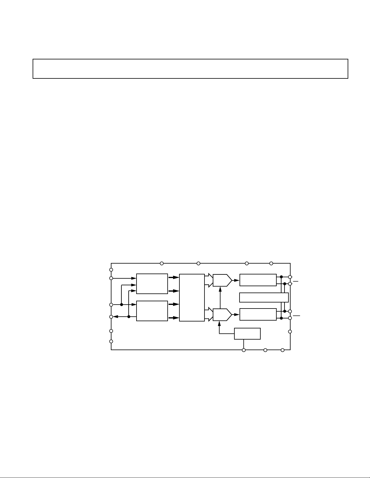
FUNCTIONAL BLOCK DIAGRAM
DGND
ANALOG MODE
SERIAL
INTERFACE
π /4 DQPSK
DIGITAL
MODULATOR
AD7011
I
Q
I
Q
V
DD
MODULATOR
BYPASS
10-BIT
I-DAC
10-BIT
Q-DAC
V
RECONSTRUCTION
CALIBRATION CIRCUITRY
RECONSTRUCTION
2.46V
REFERENCE
BYPASS
AA
FILTERS
FILTERS
AGND
MODE1
ITx
ITx
QTx
QTx
BOUT
MODE2
REV. B
Information furnished by Analog Devices is believed to be accurate and
reliable. However, no responsibility is assumed by Analog Devices for its
use, nor for any infringements of patents or other rights of third parties
which may result from its use. No license is granted by implication or
otherwise under any patent or patent rights of Analog Devices.
One Technology Way, P.O. Box 9106, Norwood, MA 02062-9106, U.S.A.
Tel: 617/329-4700 Fax: 617/326-8703

AD7011–SPECIFICATIONS
f
= 3.1104 MHz; Analog Mode, f
MCLK
Parameter AD7011ARS Units Test Conditions/Comments
DIGITAL MODE TRANSMIT SPECIFICATIONS
Number of Channels 2 (ITx –
Output Signal Range V
Differential Output Range +V
Signal Vector Magnitude
Error Vector Magnitude
Offset Vector Magnitude
IS-54 Spurious Power
2
2
2
2, 3
@ 30 kHz –35 dB typ
@ 60 kHz –70 dB typ
@ 90 kHz, 120 kHz –75 dB typ
ANALOG MODE SPECIFICATIONS
No. of Channels 2 (ITx –
Resolution 10 Bits
Output Signal Range V
Differential Output Range ±2V
DAC Update Rate 160 kHz MCLK/16; f
SNR 60 dB typ Generating a 10 kHz Sine Wave
Differential Offset Error ±15 mV max Post Calibration
Group Delay Matching Between I & Q Outputs 30 ns typ
Coding Twos Complement
Maximum and Minimum DAC Codes
= 2.56 MHz, POWER = VDD. All specifications are T
MCLK
4
(VAA = VDD = +5 V 6 10%; Test = AGND = DGND = 0 V; Digital Mode,
to T
MIN
unless otherwise noted.)
MAX
ITx) and (QTx – QTx)
+ V
REF
REF
/4 Volts For Each Analog Output
REF
/2 Volts I Channel = (ITx – ITx) and
Q Channel = (QTx –
0.875 ± 7.5% Volts max Measured Differentially
1 % rms typ
2.5 % rms max
0.5 % typ
2.5 % max
–30 dB max
–65 dB max
–70 dB max
ITx) and (QTx – QTx)
± V
REF
REF
/3 Volts For Each Analog Output
REF
/3 Volts I Channel = (ITx – ITx) and
Q Channel = (QTx –
MCLK
55 dB min
+450/–450 max/min
QTx)
QTx)
= 2.56 MHz
1
REFERENCE & CHANNEL SPECIFICATIONS
Reference, V
REF
2.46 Volts
Reference Accuracy ±5%
I and Q Gain Matching ±0.2 dB max Measured @ 10 kHz
Power-Down Option Yes Power = 0 V
LOGIC INPUTS
V
, Input High Voltage VDD – 0.9 V min
INH
V
, Input Low Voltage 0.9 V max
INL
I
, Input Current 10 FA max
INH
CIN, Input Capacitance 10 pF max
LOGIC OUTPUTS
V
Output High Voltage VDD – 0.4 V min |I
OH
VOL Output Low Voltage 0.4 V max |I
| ≤ 40 µA
OUT
| ≤ 1.6 mA
OUT
POWER SUPPLIES
V
DD
I
DD
Transmit Section Active 8 mA max POWER = V
Transmit Section Powered Down
5
4.5/5.5 V min/V max
DD
6 mA typ
35 µA max MCLK Active
5 µA max MCLK Inactive
NOTES
1
Operating temperature ranges as follows: A Version: –40°C to +85 °C.
2
See terminology.
3
Measured in continuous transmission and Burst Mode with the I and Q channels ramping up and down at the beginning and end of a burst.
4
Headroom must be allowed for the transmit DACs such that offsets in I & Q transmit channels can be calibrated out. Therefore, the full range of the I and Q DACs
are not available to the user. The user should ensure that binary codes greater than or less than the maximum or minimum are not loaded into the I or Q DACs.
5
Measured while the digital inputs to the transmit interface are static and equal to 0 V or VDD.
Specifications subject to change without notice.
–2–
REV. B

AD7011
TO OUTPUT
PIN
+2.1V
I
OH
C
L
100pF
1.6mA
200µA
I
OL
ITx/QTx
20pF
20k
Ω
AD7011
20k
Ω
Ω
ITx / QTx
20pF
40k
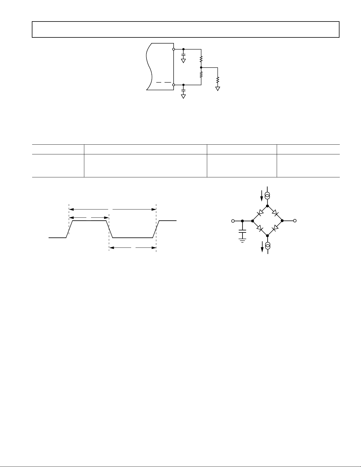
Figure 1. Analog Output Test Load Circuit
MASTER CLOCK TIMING
(VAA = VDD = +5 V 6 10%; AGND = DGND = 0 V. All specifications are T
otherwise noted.)
MIN
to T
MAX
unless
Parameter Limit at TA = –408C to +858C Units Description
t
1
t
2
t
3
t
MCLK
300 ns min MCLK Cycle Time
100 ns min MCLK High Time
100 ns min MCLK Low Time
t
1
2
t
3
Figure 2. Master Clock (MCLK) Timing
Figure 3. Load Circuit for Digital Outputs
REV. B
–3–

AD7011
(VAA = VDD = +5 V 6 10%; AGND = DGND = 0 V, f
TRANSMIT SECTION TIMING
T
to T
MIN
unless otherwise noted.)
MAX
Parameter Limit at TA = –408C to +858C Units Description
t
4
t
5
t
6
t
7
t
8
t
9
t
10
t
11
t
12
t
13
t
14
t
15
t
16
t
17
t
18
t
19
10 ns min Power Setup Time.
t
– 10 ns max
1
4097t1 + 70 ns max MCLK rising edge, after Power high, to READY rising edge.
10 ns min BIN Setup Time.
t
– 10 ns max
1
t1 + 70 ns max MCLK to READY propagation delay.
3t1 + 70 ns MCLK rising edge, after BIN high, to first TxCLK rising edge.
64t
32t
32t
1
1
1
ns TxCLK Cycle Time.
ns TxCLK High Time.
ns TxCLK Low Time.
50 ns min TxCLK falling edge to TxDATA setup time.
0 ns min TxCLK falling edge to TxDATA hold time.
3t
1
124t
7.5t
30t
1
9
1
ns max BIN low setup to Last transmitted symbol after ramp down.
ns max BIN low hold to Last transmitted symbol after ramp down.
ns Ramp Down cycle time after the last transmitted symbol.
ns max Last TxCLK falling edge to READY rising edge.
10 ns max Digital Output Rise Time.
10 ns max Digital Output Fall Time.
= 3.1104 MHz. All specifications are
MCLK
MCLK
POWER
READY
BIN
TxCLK
TxDATA
MCLK
POWER
READY
BIN
TxCLK
TxDATA
t
t
4
t
5
7
t
6
t
t
8
9
t
11
t
12
t
13
X
k
t
10
Y
k
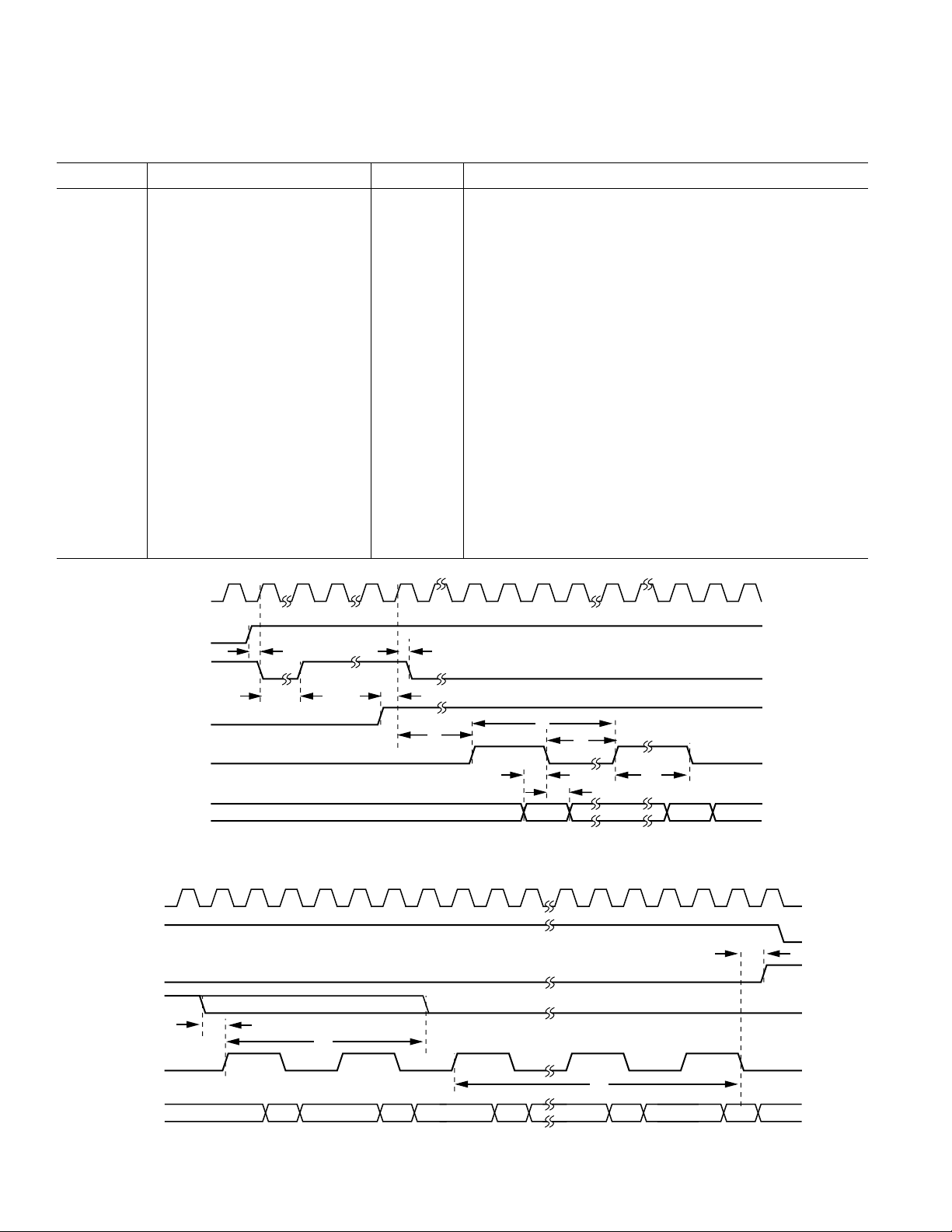
Figure 4. Transmit Timing at the Start of a Tx Burst
t
17
t
14
t
15
t
16
X
N+4
Y
N+4
X
N+5
X
N+8
Y
N+8
Figure 5. Transmit Timing at the End of a Tx Burst
–4–
REV. B
 Loading...