Analog Devices AD7010 Datasheet

CMOS
a
FEATURES
Single +5 V Supply
On-Chip p/4 DQPSK Modulator
Root-Raised-Cosine Tx Filters, a = 0.5
Two 10-Bit D/A Converters
4th Order Reconstruction Filters
Differential Analog Outputs
On-Chip Ramp Up/Down Power Control
On-Chip Tx Offset Calibration
Very Low Power Dissipation, 30 mW typ
Power Down Mode < 5 mA
On-Chip Voltage Reference
24-Pin SSOP
APPLICATIONS
Japanese Digital Cellular Telephony
JDC p/4 DQPSK Baseband T ransmit Port
AD7010
GENERAL DESCRIPTION
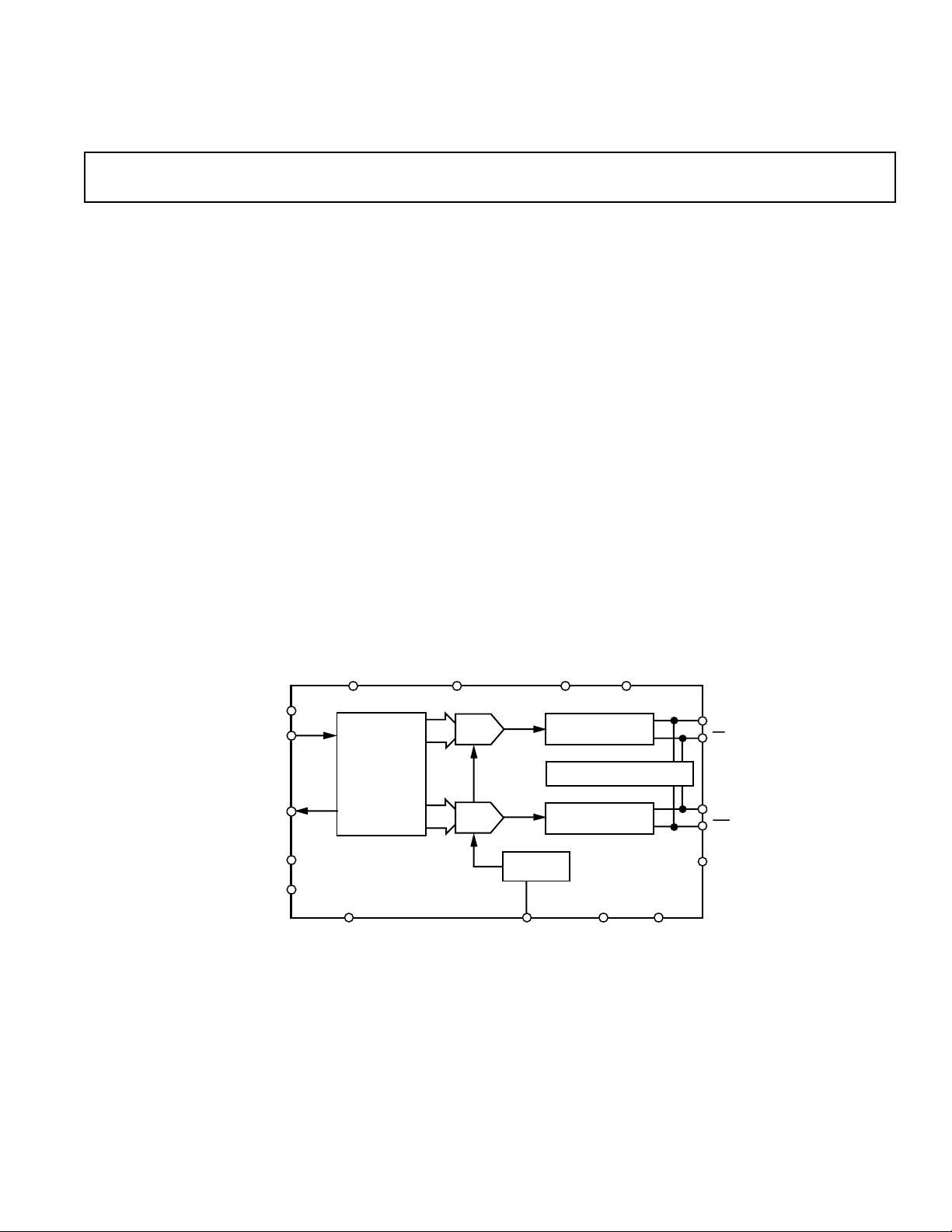
The AD7010 is a complete low power, CMOS, π/4 DQPSK
modulator with single +5 V power supply. The part is designed
to perform the baseband conversion of I and Q transmit
waveforms in accordance with the Japanese Digital Cellular
Telephone system.
The on-chip π/4 Differential Quadrature Phase Shift Keying
(DQPSK) digital modulator, which includes the Root Raised
Cosine filters, generates I and Q data in response to the transmit
data stream. The AD7010 also contains ramp control envelope
logic to shape the I and Q output waveforms when ramping up
or down at the beginning or end of a transmit burst.
Besides providing all the necessary logic to perform π/4 DQPSK
modulation, the part also provides reconstruction filters to
smooth the DAC outputs, providing continuous time analog
outputs. The AD7010 generates differential analog outputs for
both the I and Q signals.
As it is a necessity for all digital mobile systems to use the lowest
possible power, the device has power down options. The
AD7010 is housed in a space efficient 24-pin SSOP (Shrink
Small Outline Package).
POWER
Tx DATA
Tx CLK
READY
BIN
FUNCTIONAL BLOCK DIAGRAM
V
DGND
π/4 DQPSK
MODULATOR
AD7010
MCLK
DD
10-BIT
I-DAC
10-BIT
Q-DAC
REFERENCE
BYPASS
V
AA
RECONSTRUCTION
FILTERS
CALIBRATION CIRCUITRY
RECONSTRUCTION
FILTERS
2.46V
MODE1
AGND
ITx
ITx
QTx
QTx
BOUT
MODE2
REV. B
Information furnished by Analog Devices is believed to be accurate and
reliable. However, no responsibility is assumed by Analog Devices for its
use, nor for any infringements of patents or other rights of third parties
which may result from its use. No license is granted by implication or
otherwise under any patent or patent rights of Analog Devices.
One Technology Way, P.O. Box 9106, Norwood, MA 02062-9106, U.S.A.
Tel: 617/329-4700 Fax: 617/326-8703

AD7010–SPECIFICATIONS
(VAA = VDD = +5 V 6 10%; Test = AGND = DGND = 0 V; f
1
Power = VDD. All specifications are T
MIN
to T
MAX
unless otherwise noted.)
= 2.688 MHz;
MCLK
Parameter AD7010ARS Units Test Conditions/Comments
DIGITAL MODE TRANSMIT
No. of Channels 2 (ITx–
Output Signal Range V
Differential Output Range ±V
Signal Vector Magnitude
Error Vector Magnitude
Offset Vector Magnitude
JDC Spurious Power
2
2
2
2, 3
± V
REF
REF
/4 Volts For Each Analog Output
REF
/2 Volts I Channel = (ITx–ITx)
0.875 ± 7.5% Volts max Measured Differentially
1 % rms typ
2.5 % rms max
0.5 % typ
2.5 % max
ITx) and (QTx–QTx)
and Q Channel = (QTx–
QTx)
@ 25 kHz –30 dB typ
–25 dB max
@ 50 kHz –60 dB typ
–55 dB max
@ 75 kHz –70 dB typ
–65 dB max
@ 100 kHz, 150 kHz, 200 kHz –70 dB typ
–65 dB max
REFERENCE & CHANNEL SPECIFICATIONS
Reference, V
REF
2.46 Volts
Reference Accuracy ±5%
I and Q Gain Matching ±0.2 dB max Measured @ 10 kHz
Power Down Option Yes Power = 0 V
LOGIC INPUTS
V
, Input High Voltage VDD–0.9 V min
INH
V
, Input Low Voltage 0.9 V max
INL
I
, Input Current 10 µA max
INH
CIN, Input Capacitance 10 pF max
LOGIC OUTPUTS
V
, Output High Voltage VDD–0.4 V min |I
OH
VOL, Output Low Voltage 0.4 V max |I
| ≤ 40 µA
OUT
| ≤ 1.6 mA
OUT
POWER SUPPLIES
V
DD
I
DD
Transmit Section Active 8 mA max Power = V
Transmit Section Powered Down
4
4.5/5.5 V min/V max
DD
6 mA typ
35 µA max MCLK Active
5 µA max MCLK Inactive
NOTES
1
Operating temperature ranges as follows: A Version: –40°C to +85 °C.
2
See Terminology.
3
Measured in continuous transmission and Burst transmission with the I and Q channels ramping up and down at the beginning and end of each burst.
4
Measured while the digital inputs to the transmit interface are static and equal to 0 V or VDD.
Specifications subject to change without notice.
ORDERING GUIDE
Model Temperature Range Package Description Package Option
AD7010ARS –40°C to +85°C Shrink Small Outline Package RS-24
–2–
REV. B

20kΩ
20kΩ
20pF
20pF
AD7010
ITx/QTx
40kΩ
ITx / QTx
Q
I
MODULAR OUTPUT
DURING FTEST
ABSOLUTE MAXIMUM RATINGS*
WARNING!
ESD SENSITIVE DEVICE
TO OUTPUT
PIN
+2.1V
I
OH
C
L
100pF
1.6mA
200µA
I
OL
(TA = +25°C unless otherwise noted)
VDD Tx, VDD Rx to AGND . . . . . . . . . . . . . . . –0.3 V to +7 V
AGND to DGND . . . . . . . . . . . . . . . . . . . . .–0.3 V to +0.3 V
Digital I/O Voltage to DGND . . . . . –0.3 V to V
Analog I/O Voltage to AGND . . . . . . . –0.3 V to V
to + 0.3 V
DD
+ 0.3 V
DD
Operating Temperature Range
Industrial (A Version) . . . . . . . . . . . . . . . . –40°C to +85°C
Storage Temperature Range . . . . . . . . . . . . –65°C to +150°C
Junction Temperature . . . . . . . . . . . . . . . . . . . . . . . . +150°C
SSOP θ
Thermal Impedance . . . . . . . . . . . . . . . . +122°C/W
JA
Lead Temperature, Soldering
Vapor Phase (60 sec) . . . . . . . . . . . . . . . . . . . . . +215°C
Infrared (15 sec) . . . . . . . . . . . . . . . . . . . . . . . . . +220°C
*Stresses above those listed under “Absolute Maximum Ratings” may cause
permanent damage to the device. This is a stress rating only and functional
operation of the device at these or any other conditions above those listed in the
operational sections of this specification is not implied. Exposure to absolute
maximum rating conditions for extended periods may affect device reliability.
Table I.
MODE 1 MODE 2 Operation
AD7010
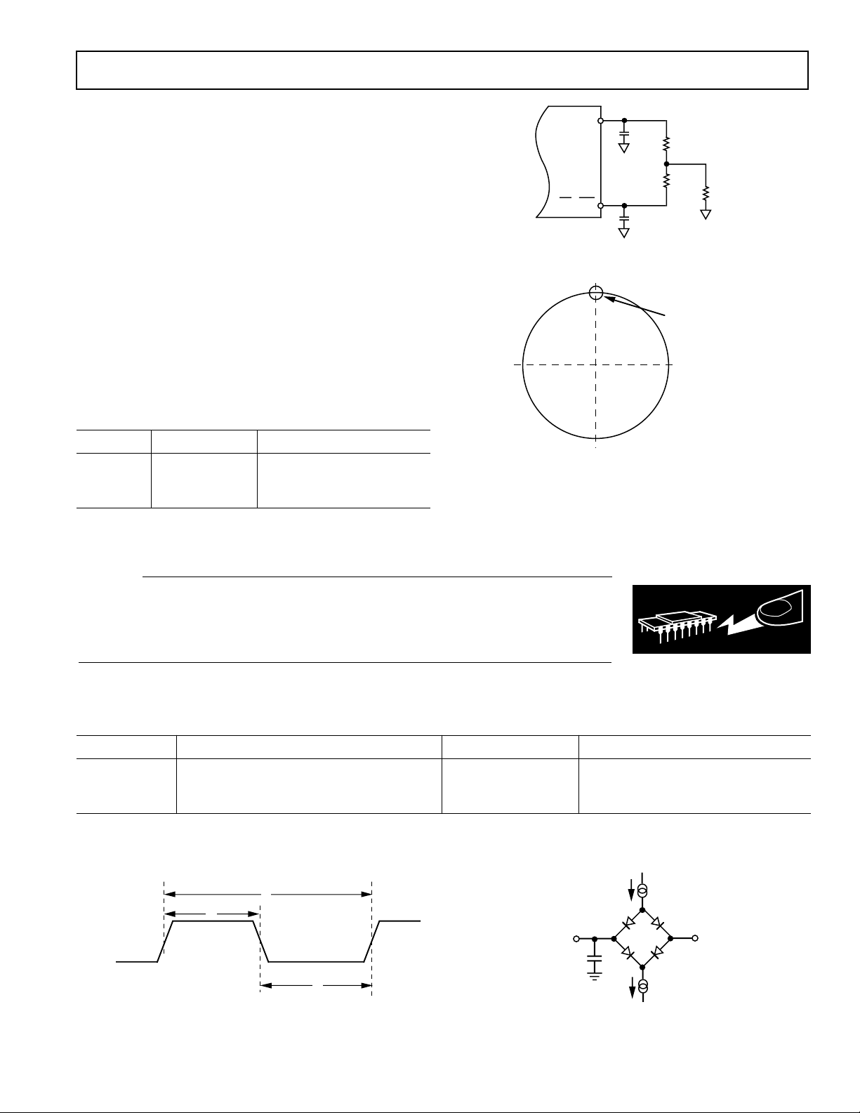
Figure 1. Analog Output Load Test Circuit
0 0 Digital JDC Mode
0 1 FTEST
Figure 2. Modulator State During FTEST
1 X Factory Test, Reserved
CAUTION
ESD (electrostatic discharge) sensitive device. Electrostatic charges as high as 4000 V readily
accumulate on the human body and test equipment and can discharge without detection.
Although the AD7010 features proprietary ESD protection circuitry, permanent damage may
occur on devices subjected to high energy electrostatic discharges. Therefore, proper ESD
precautions are recommended to avoid performance degradation or loss of functionality.
MASTER CLOCK TIMING
(VAA = VDD = +5 V 6 10%; AGND = DGND = O V. All specifications are T
otherwise noted.)
MIN
to T
MAX
unless
Parameter Limit at TA = –408C to +858C Units Description
t
1
t
2
t
3
300 ns min MCLK Cycle Time
100 ns min MCLK High Time
100 ns min MCLK Low Time
MCLK
Figure 3. Master Clock (MCLK) Timing
REV. B
t
1
t
2
t
3
Figure 4. Load Circuit for Digital Outputs
–3–
 Loading...