

ANALOG DEVICES AD629 Service Manual
High Common-Mode Voltage,
R
A
www.BDTIC.com/ADI
FEATURES
Improved replacement for: INA117P and INA117KU
±270 V common-mode voltage range
Input protection to
±500 V common mode
±500 V differential mode
Wide power supply range (±2.5 V to ±18 V)
±10 V output swing on ±12 V supply
1 mA maximum power supply current
HIGH ACCURACY DC PERFORMANCE
3 ppm maximum gain nonlinearity (AD629B)
20 μV/°C maximum offset drift (AD629A)
10 μV/°C maximum offset drift (AD629B)
10 ppm/°C maximum gain drift
EXCELLENT AC SPECIFICATIONS
77 dB minimum CMRR @ 500 Hz (AD629A)
86 dB minimum CMRR @ 500 Hz (AD629B)
500 kHz bandwidth
APPLICATIONS
High voltage current sensing
Battery cell voltage monitors
Power supply current monitors
Motor controls
Isolation
100
95
90
TIO (dB)
85
80
75
70
65
60
COMMON-MO DE REJECTIO N
55
50
20 100 1k 10k 20k
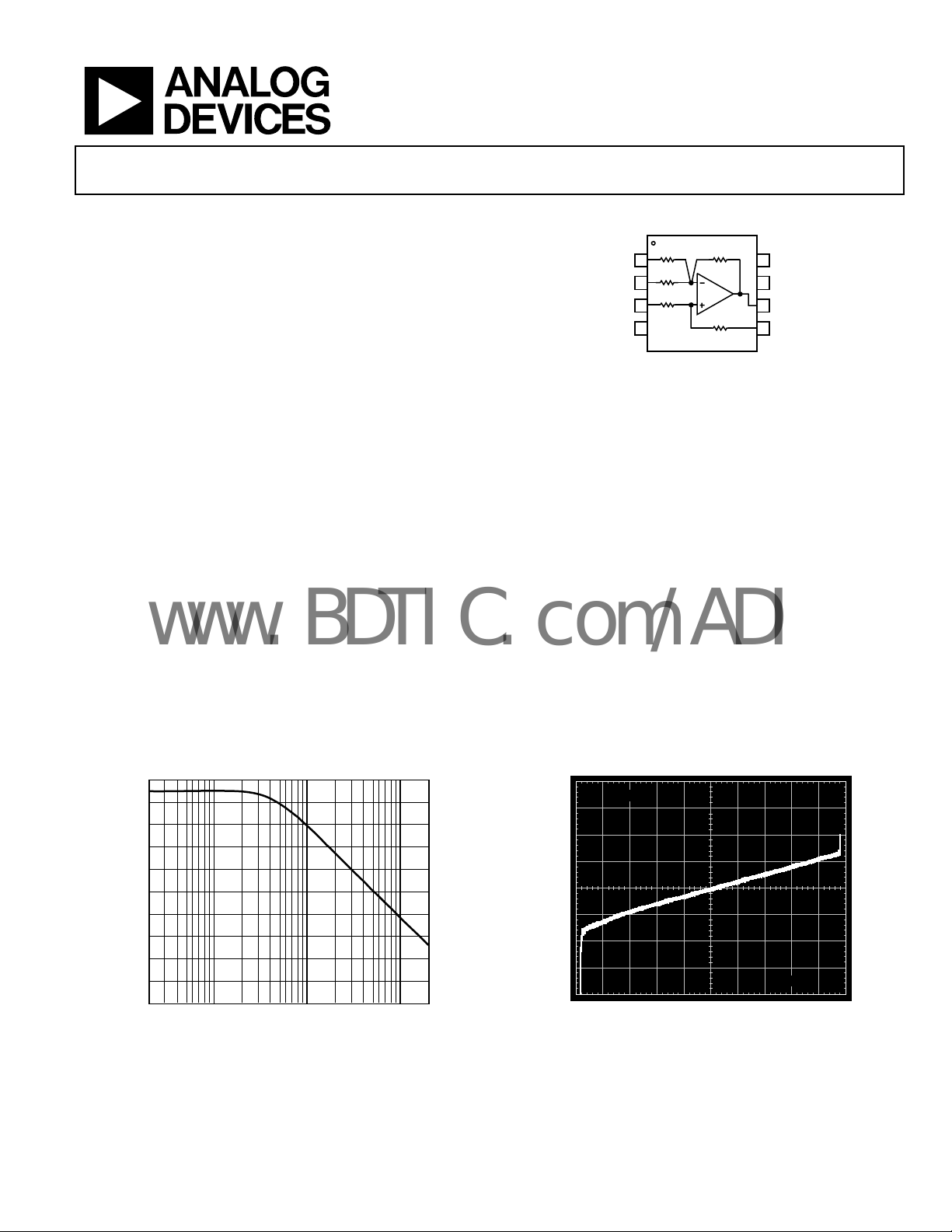
Figure 2. Common-Mode Rejection Ratio vs. Frequency
FREQUENCY ( Hz)
Difference Amplifier
AD629
FUNCTIONAL BLOCK DIAGRAM
REF(–)
–V
–IN
+IN
2
3
4
S
380kΩ
380kΩ
AD629
NC = NO CONNECT
21.1kΩ
1
GENERAL DESCRIPTION
The AD629 is a difference amplifier with a very high input,
common-mode voltage range. It is a precision device that allows
the user to accurately measure differential signals in the
presence of high common-mode voltages up to ±270 V.
The AD629 can replace costly isolation amplifiers in
pplications that do not require galvanic isolation. The device
a
operates over a ±270 V common-mode voltage range and has
inputs that are protected from common-mode or differential
mode transients up to ±500 V.
The AD629 has low offset, low offset drift, low gain error drift,
w common-mode rejection drift, and excellent CMRR over a
lo
wide frequency range.
The AD629 is available in low cost, 8-lead PDIP and 8-lead
SO
IC packages. For all packages and grades, performance is
guaranteed over the industrial temperature range of −40°C to
+85°C.
2mV/DIV
OUTPUT ERROR (2mV/DIV)
00783-002
–240 240120–120 0
Figure 3. Error Voltage vs. Input Common-Mode Voltage
COMMON-MODE VOLTAGE (V)
380kΩ
20kΩ
Figure 1.
NC
8
7
+V
6
OUTPUT
5
REF(+)
60V/DIV
S
0783-001
00783-003
Rev. B
Information furnished by Analog Devices is believed to be accurate and reliable. However, no
responsibility is assumed by Anal og Devices for its use, nor for any infringements of patents or ot her
rights of third parties that may result from its use. Specifications subject to change without notice. No
license is granted by implication or otherwise under any patent or patent rights of Analog Devices.
Trademarks and registered trademarks are the property of their respective owners.
One Technology Way, P.O. Box 9106, Norwood, MA 02062-9106, U.S.A.
Tel: 781.329.4700 www.analog.com
Fax: 781.461.3113 ©1999-2007 Analog Devices, Inc. All rights reserved.

AD629
www.BDTIC.com/ADI
TABLE OF CONTENTS
Features .............................................................................................. 1
Applications....................................................................................... 1
Functional Block Diagram .............................................................. 1
General Description......................................................................... 1
Revision History ............................................................................... 2
Specifications..................................................................................... 3
Absolute Maximum Ratings............................................................ 4
ESD Caution.................................................................................. 4
Typical Performance Characteristics ............................................. 5
Theory of Operation ........................................................................ 9
Applications..................................................................................... 10
REVISION HISTORY
3/07—Rev. A to Rev. B
Updated Format and Layout .............................................Universal
Changes to Ordering Guide.......................................................... 15
3/00—Rev. 0 to Rev. A
10/99—Revision 0: Initial Version
Basic Connections...................................................................... 10
Single-Supply Operation ........................................................... 10
System-Level Decoupling and Grounding.............................. 10
Using a Large Sense Resistor..................................................... 11
Output Filtering.......................................................................... 11
Output Current and Buffering.................................................. 12
A Gain of 19 Differential Amplifier......................................... 12
Error Budget Analysis Example 1 ............................................ 12
Error Budget Analysis Example 2 ............................................ 13
Outline Dimensions ....................................................................... 14
Ordering Guide............................................................................... 15
Rev. B | Page 2 of 16
AD629
www.BDTIC.com/ADI
SPECIFICATIONS
TA = 25°C, VS = ±15 V, unless otherwise noted.
Table 1.
AD629A AD629B
Parameter Condition Min Typ Max Min Typ Max Unit
GAIN V
= ±10 V, RL = 2 kΩ
OUT
Nominal Gain 1 1 V/V
Gain Error 0.01 0.05 0.01 0.03 %
Gain Nonlinearity 4 10 4 10 ppm
R
Gain vs. Temperature TA = T
= 10 kΩ 1 1 3 ppm
L
to T
MIN
3 10 3 10 ppm/°C
MAX
OFFSET VOLTAGE
Offset Voltage 0.2 1 0.1 0.5 mV
V
vs. Temperature TA = T
= ±5 V 1 mV
S
to T
MIN
6 20 3 10 μV/°C
MAX
vs. Supply (PSRR) VS = ±5 V to ± 15 V 84 100 90 110 dB
INPUT
Common-Mode Rejection Ratio VCM = ±250 V dc 77 88 86 96 dB
T
V
V
= T
to T
A
MIN
= 500 V p-p, dc to 500 Hz 77 86 dB
CM
= 500 V p-p, dc to 1 kHz 88 90 dB
CM
73 82 dB
MAX
Operating Voltage Range Common mode ±270 ±270 V
Differential ±13 ±13 V
Input Operating Impedance Common mode 200 200 kΩ
Differential 800 800 kΩ
OUTPUT
Operating Voltage Range RL = 10 kΩ ±13 ±13 V
R
V
= 2 kΩ ±12.5 ±12.5 V
L
= ±12 V, RL = 2 kΩ ±10 ±10 V
S
Output Short-Circuit Current ±25 ±25 mA
Capacitive Load Stable operation 1000 1000 pF
DYNAMIC RESPONSE
Small Signal –3 dB Bandwidth 500 500 kHz
Slew Rate 1.7 2.1 1.7 2.1 V/μs
Full Power Bandwidth V
Settling Time 0.01%, V
0.1%, V
0.01%, VCM = 10 V step, V
= 20 V p-p 28 28 kHz
OUT
= 10 V step 15 15 μs
OUT
= 10 V step 12 12 μs
OUT
= 0 V 5 5 μs
DIFF
OUTPUT NOISE VOLTAGE
0.01 Hz to 10 Hz 15 15 μV p-p
Spectral Density, ≥100 Hz
1
550 550 nV/√Hz
POWER SUPPLY
Operating Voltage Range ±2.5 ±18 ±2.5 ±18 V
Quiescent Current V
T
= 0 V 0.9 1 0.9 1 mA
OUT
MIN
to T
MAX
1.2 1.2 mA
TEMPERATURE RANGE
For Specified Performance TA = T
1
See Figure 19.
MIN
to T
MAX
−40 +85 −40 +85 °C
Rev. B | Page 3 of 16
AD629
A
www.BDTIC.com/ADI
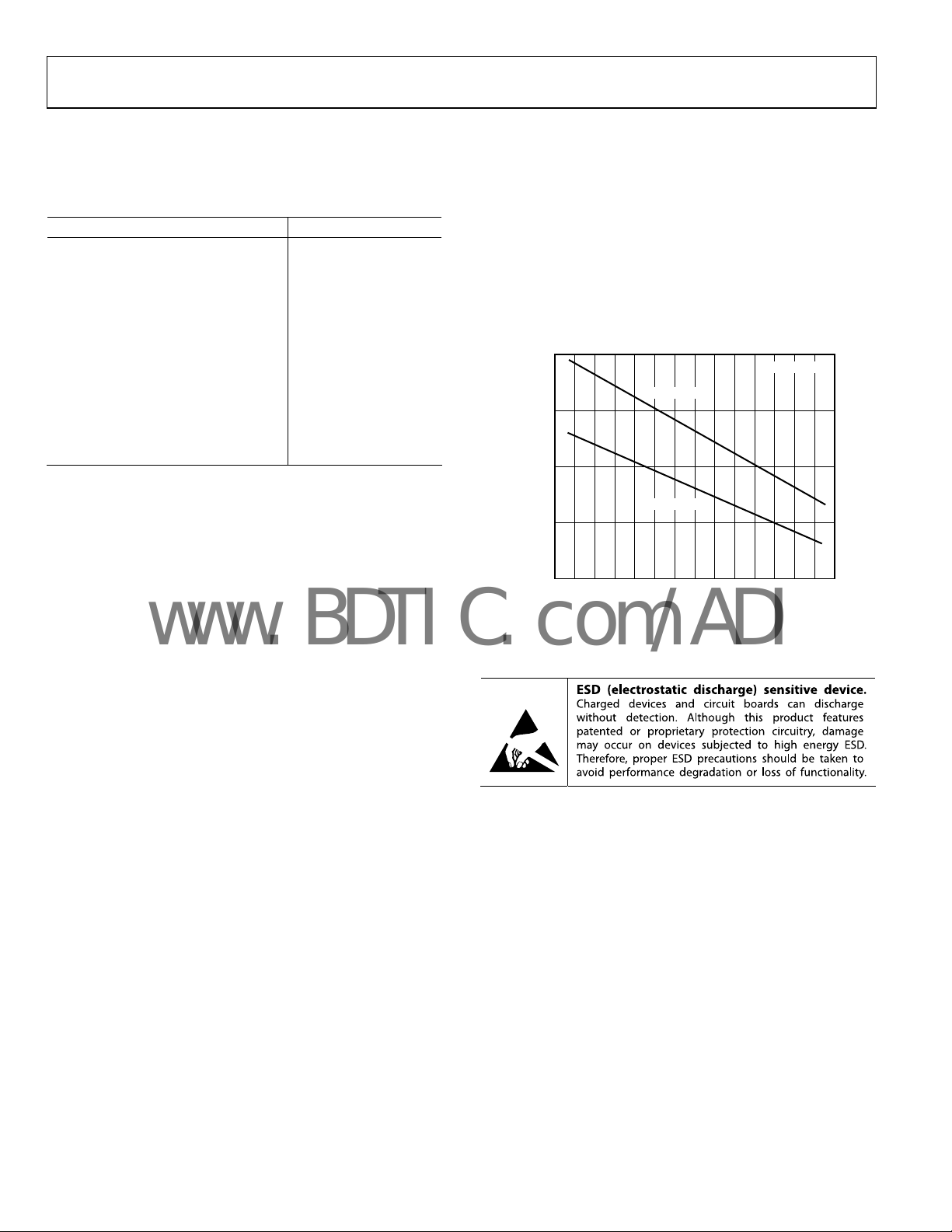
ABSOLUTE MAXIMUM RATINGS
Table 2.
Parameter Rating
Supply Voltage, V
Internal Power Dissipation
8-Lead PDIP (N) See Figure 4
8-Lead SOIC (R) See Figure 4
Input Voltage Range, Continuous ±300 V
Common-Mode and Differential, 10 sec ±500 V
Output Short-Circuit Duration Indefinite
Pin 1 and Pin 5 –VS − 0.3 V to +VS + 0.3 V
Maximum Junction Temperature 150°C
Operating Temperature Range −55°C to +125°C
Storage Temperature Range −65°C to +150°C
Lead Temperature (Soldering 60 sec) 300°C
1
Specification is for device in free air:
8-Lead PDIP, θJA = 100°C/W;
8-Lead SOIC, θJA = 155°C/W.
S
1
±18 V
Stresses above those listed under Absolute Maximum Ratings
may cause permanent damage to the device. This is a stress
rating only; functional operation of the device at these or any
other conditions above those indicated in the operational
section of this specification is not implied. Exposure to absolute
maximum rating conditions for extended periods may affect
device reliability.
Figure 4. Maximum Power Dissipation vs. Temperature for SOIC and PDIP
2.0
8-LEAD PDIP
1.5
TION (W)
1.0
8-LEAD SOI C
0.5
MAXIMUM POWER DISSIP
0
–50 –40 –30 –20 –10 0 10 20 30 40 50 60 70 80 90
AMBIENT TEMPERATURE (°C)
TJ = 150°C
00783-004
ESD CAUTION
Rev. B | Page 4 of 16
AD629
R
A
www.BDTIC.com/ADI
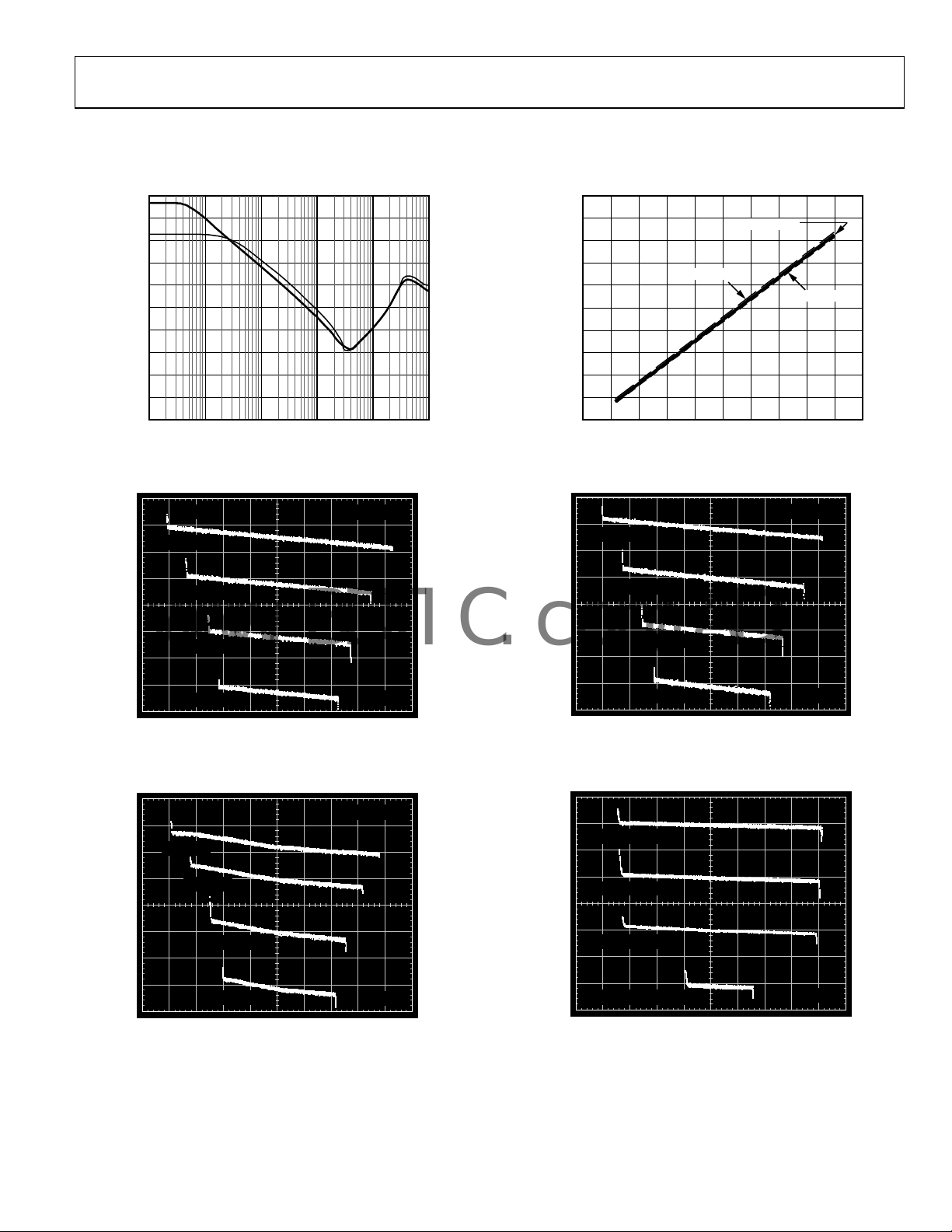
TYPICAL PERFORMANCE CHARACTERISTICS
TA = 25°C, VS = ±15 V, unless otherwise noted.
100
90
80
TIO (dB)
70
60
50
40
30
20
10
COMMON-M ODE REJECTI ON
0
100 1k 10k 100k 1M 10M
FREQUENCY ( Hz)
Figure 5. Common-Mode Rejection Ratio vs. Frequency
00783-006
400
360
320
280
240
200
160
120
80
COMMON-MODE VOLTAGE (±V)
40
0
02 6 104 8 12 14 1816 20
TA = +85°C
POWER SUPPLY VOLTAGE (±V)
TA = +25°C
TA = –40°C
Figure 8. Common-Mode Operating Range vs. Power Supply Voltage
00783-009
2mV/DIV
VS = ±18V
VS = ±15V
VS = ±12V
OUTPUT ERROR (2mV/DIV)
VS = ±10V
–20 –16 –8 –4 0 4 8 12 16–12 20
Figure 6. Typical Gain Error Normalized @ V
Operating Range vs. Supply Voltage, R
VS = ±18V
VS = ±15V
VS = ±12V
OUTPUT ERROR (2mV/DIV)
V
(V)
OUT
= 0 V and Output Voltage
OUT
= 10 kΩ (Curves Offset for Clarity)
L
RL = 10kΩ
4V/DIV
RL = 1kΩ
RL = 2kΩ
VS = ±18V
VS = ±15V
VS = ±12V
OUTPUT ERROR (2mV/DIV)
VS = ±10V
00783-007
–20 –16 –8 –4 0 4 8 12 16–12 20
Figure 9. Typical Gain Error Normalized @ V
Operating Range vs. Supply Voltage, R
VS = ±5V, RL = 10kΩ
VS = ±5V, RL = 2kΩ
VS = ±5V, RL = 1kΩ
OUTPUT ERROR (2mV/DIV)
V
(V)
OUT
= 0 V and Output Voltage
OUT
= 2 kΩ (Curves Offset for Clarity)
L
4V/DIV
00783-010
VS = ±10V
–20 –16 –8 –4 0 4 8 12 16–12 20
Figure 7. Typical Gain Error Normalized @ V
Operating Range vs. Supply Voltage, R
V
(V)
OUT
= 0 V and Output Voltage
OUT
= 1 kΩ (Curves Offset for Clarity)
L
4V/DIV
00783-008
Figure 10. Typical Gain Error Normalized @ V
VS = ±2.5V, RL = 1kΩ
–20 –16 –8 –4 0 4 8 12 16–12 20
Operating Range vs. Supply Voltage (Curves Offset for Clarity)
Rev. B | Page 5 of 16
1V/DIV
00783-011
V
(V)
OUT
= 0 V and Output Voltage
OUT
 Loading...