

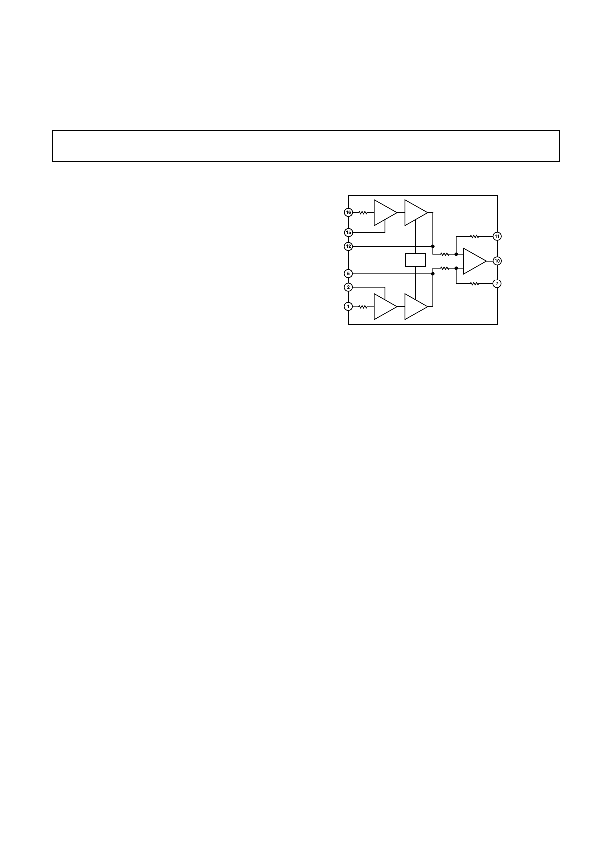
FUNCTIONAL BLOCK DIAGRAM
+
–
+
–
+
–
+
–
+
–
50
50
10k
10k
10k
10k
V
B
–INPUT
–GAIN
SENSE
+INPUT
–GAIN
DRIVE
+GAIN
SENSE
+GAIN
DRIVE
SENSE
OUTPUT
REFERENCE
AD625
REV. D
Information furnished by Analog Devices is believed to be accurate and
reliable. However, no responsibility is assumed by Analog Devices for its
use, nor for any infringements of patents or other rights of third parties
which may result from its use. No license is granted by implication or
otherwise under any patent or patent rights of Analog Devices.
a
Programmable Gain
Instrumentation Amplifier
AD625
One Technology Way, P.O. Box 9106, Norwood, MA 02062-9106, U.S.A.
Tel: 781/329-4700 World Wide Web Site: http://www.analog.com
Fax: 781/326-8703 © Analog Devices, Inc., 2000
FEATURES
User Programmed Gains of 1 to 10,000
Low Gain Error: 0.02% Max
Low Gain TC: 5 ppm/C Max
Low Nonlinearity: 0.001% Max
Low Offset Voltage: 25 V
Low Noise 4 nV/√Hz (at 1 kHz) RTI
Gain Bandwidth Product: 25 MHz
16-Lead Ceramic or Plastic DIP Package,
20-Terminal LCC Package
Standard Military Drawing Available
MlL-Standard Parts Available
Low Cost
PRODUCT DESCRIPTION
The AD625 is a precision instrumentation amplifier specifically
designed to fulfill two major areas of application: 1) Circuits requiring nonstandard gains (i.e., gains not easily achievable with
devices such as the AD524 and AD624). 2) Circuits requiring a
low cost, precision software programmable gain amplifier.
For low noise, high CMRR, and low drift the AD625JN is the
most cost effective instrumentation amplifier solution available.
An additional three resistors allow the user to set any gain from
1 to 10,000. The error contribution of the AD625JN is less than
0.05% gain error and under 5 ppm/°C gain TC; performance
limitations are primarily determined by the external resistors.
Common-mode rejection is independent of the feedback resistor
matching.
A software programmable gain amplifier (SPGA) can be configured with the addition of a CMOS multiplexer (or other switch
network), and a suitable resistor network. Because the ON
resistance of the switches is removed from the signal path, an
AD625 based SPGA will deliver 12-bit precision, and can be
programmed for any set of gains between 1 and 10,000, with
completely user selected gain steps.
For the highest precision the AD625C offers an input offset
voltage drift of less than 0.25 µV/°C, output offset drift below
15 µV/°C, and a maximum nonlinearity of 0.001% at G = 1. All
grades exhibit excellent ac performance; a 25 MHz gain bandwidth product, 5 V/µs slew rate and 15 µs settling time.
The AD625 is available in three accuracy grades (A, B, C) for
industrial (–40°C to +85°C) temperature range, two grades (J,
K) for commercial (0°C to +70°C) temperature range, and one
(S) grade rated over the extended (–55°C to +125°C) temperature range.
PRODUCT HIGHLIGHTS
1. The AD625 affords up to 16-bit precision for user selected
fixed gains from 1 to 10,000. Any gain in this range can be
programmed by 3 external resistors.
2. A 12-bit software programmable gain amplifier can be configured using the AD625, a CMOS multiplexer and a resistor
network. Unlike previous instrumentation amplifier designs,
the ON resistance of a CMOS switch does not affect the gain
accuracy.
3. The gain accuracy and gain temperature coefficient of the
amplifier circuit are primarily dependent on the user selected
external resistors.
4. The AD625 provides totally independent input and output
offset nulling terminals for high precision applications. This
minimizes the effects of offset voltage in gain-ranging
applications.
5. The proprietary design of the AD625 provides input voltage
noise of 4 nV/√Hz at 1 kHz.
6. External resistor matching is not required to maintain high
common-mode rejection.

AD625A/J/S AD625B/K AD625C
Model Min Typ Max Min Typ Max Min Typ Max Unit
GAIN
Gain Equation
2 R
F
R
G
+ 1
2 R
F
R
G
+ 1
2 R
F
R
G
+ 1
Gain Range 1 10,000 1 10,000 1 110,000
Gain Error
1
±.0350.05 ±0.020.03 ±0.010.02 %
Nonlinearity, Gain = 1-256 ±0.005 ± 0.002 ±0.001 %
Gain>256 ±0.01 ±0.008 ±0.005 %
Gain vs. Temp. Gain<1000
1
5 5 5 ppm/°C
GAIN SENSE INPUT
Gain Sense Current 300 500 150 250 50 100 nA
vs. Temperature 5 20 2 15 2 10 nA/°C
Gain Sense Offset Current 150 500 75 250 50 100 nA
vs. Temperature 2 15 1 10 2 10 nA/°C
VOLTAGE OFFSET (May be Nulled)
Input Offset Voltage 50 200 25 50 10 25 µV
vs. Temperature 1 2/2 0.25 0.50/1 0.1 0.25 µV/°C
Output Offset Voltage 4 5 2 3 1 2 mV
vs. Temperature 20 50/50 10 25/40 10 15 µV/°C
Offset Referred to the
Input vs. Supply
G = 1 70 75 75 85 80 90 dB
G = 10 85 95 90 100 95 105 dB
G = 100 95 100 105 110 110 120 dB
G = 1000 100 110 110 120 115 140 dB
INPUT CURRENT
Input Bias Current ±30
50 ±20
25 ±10
15 nA
vs. Temperature ±50 ±50 ± 50 pA/°C
Input Offset Current ±2
35 ±1
15 ±1
5 nA
vs. Temperature ±20 ±20 ± 20 pA/°C
INPUT
Input Impedance
Differential Resistance 1 1 1 GΩ
Differential Capacitance 4 4 4 pF
Common-Mode Resistance 1 1 1 GΩ
Common-Mode Capacitance 4 4 4 pF
Input Voltage Range
Differ. Input Linear (V
DL
)
2
±10 ±10 ± 10 V
Common-Mode Linear (V
CM
)
12 V –
G
2
×V
D
(
)
12 V –
G
2
×V
D
(
)
12 V –
G
2
×V
D
(
)
Common-Mode Rejection Ratio dc to
60 Hz with 1 kΩ Source Imbalance
G = 1 70 75 75 85 80 90 dB
G = 10 90 95 90 105 100 115 dB
G = 100 100 105 105 115 110 125 dB
G = 1000 110 115 110 125 120 140 dB
OUTPUT RATING ± 10 V ±10 V ±10 V
@ 5 mA @ 5 mA @ 5 mA
DYNAMIC RESPONSE
Small Signal –3 dB
G = 1 (RF = 20 kΩ) 650 650 650 kHz
G = 10 400 400 400 kHz
G = 100 150 150 150 kHz
G = 1000 25 25 25 kHz
Slew Rate 5.0 5.0 5.0 V/µs
Settling Time to 0.01%, 20 V Step
G = 1 to 200 15 15 15 µs
G = 500 35 35 35 µs
G = 1000 75 75 75 µs
AD625–SPECIFICATIONS
(typical @ VS = 15 V, RL = 2 k and TA = + 25C, unless otherwise noted)
REV. D
–2–

AD625
AD625A/J/S AD625B/K AD625C
Model Min Typ Max Min Typ Max Min Typ Max Unit
NOISE
Voltage Noise, 1 kHz
R.T.I. 4 4 4 nV/√Hz
R.T.O. 75 75 75 nV/√Hz
R.T.I., 0.1 Hz to 10 Hz
G = 1 10 10 10 µV p-p
G = 10 1.0 1.0 1.0 µV p-p
G = 100 0.3 0.3 0.3 µV p-p
G = 1000 0.2 0.2 0.2 µV p-p
Current Noise
0.1 Hz to 10 Hz 60 60 60 pA p-p
SENSE INPUT
R
IN
10 10 10 kΩ
I
IN
30 30 30 µA
Voltage Range ± 10 ± 10 ±10 V
Gain to Output 1 ± 0.01 1 ± 0.01 1 ± 0.01 %
REFERENCE INPUT
R
IN
20 20 20 kΩ
I
IN
30 30 30 µA
Voltage Range ± 10 ± 10 ±10 V
Gain to Output 1 ± 0.01 1 ± 0.01 1 ± 0.01 %
TEMPERATURE RANGE
Specified Performance
J/K Grades 0 +70 0 +70 °C
A/B/C Grades –40 +85 –40 +85 –40 +85 °C
S Grade –55 +125 °C
Storage –65 +150 –65 +150 –65 +150 °C
POWER SUPPLY
Power Supply Range ±6 to ± 18 ±6 to ±18 ± 6 to ± 18 V
Quiescent Current 3.5 5 3.5 5 3.5 5 mA
NOTES
1
Gain Error and Gain TC are for the AD625 only. Resistor Network errors will add to the specified errors.
2
VDL is the maximum differential input voltage at G = 1 for specified nonlinearity. VDL at other gains = 10 V/G. VD = actual differential input voltage.
Example: G = 10, VD = 0.50; VCM = 12 V – (10/2 × 0.50 V) = 9.5 V.
Specifications subject to change without notice.
All min and max specifications are guaranteed. Specifications shown in boldface are tested on all production units at final electrical test. Results from those tests are
used to calculate outgoing quality levels.
REV. D
–3–
AD625
REV. D–4–
PIN CONNECTIONS
Ceramic DIP (D) and Plastic DIP (N) Packages
TOP VIEW
(Not to Scale)
NC = NO CONNECT
+INPUT –INPUT
AD625
+GAIN SENSE –GAIN SENSE
RTI NULL RTO NULL
RTI NULL RTO NULL
+GAIN DRIVE
–GAIN DRIVE
NC SENSE
REFERENCE V
OUT
–V
S
+V
S
10k 10k+V
S
–V
S
1
2
3
4
5
6
7
8
16
15
14
13
12
11
10
9
Leadless Chip Carrier (E) Package
20 19123
18
14
15
16
17
4
5
6
7
8
910111213
TOP VIEW
(Not to Scale)
AD625
RTI NULL
RTI NULL
NC
+GAIN DRIVE
NC
RTO NULL
RTO NULL
NC
–GAIN NULL
SENSE
NC = NO CONNECT
+INPUT
REFERENCE
–V
S
NC
+V
S
NC
+GAIN SENSE
–GAIN SENSE
V
OUT
–INPUT
ABSOLUTE MAXIMUM RATINGS*
Supply Voltage . . . . . . . . . . . . . . . . . . . . . . . . . . . . . . . . . ± 18 V
Internal Power Dissipation . . . . . . . . . . . . . . . . . . . . . . 450 mW
Input Voltage . . . . . . . . . . . . . . . . . . . . . . . . . . . . . . . . . . . ±V
S
Differential Input Voltage . . . . . . . . . . . . . . . . . . . . . . . . . ±V
S
Output Short Circuit Duration . . . . . . . . . . . . . . . . Indefinite
Storage Temperature Range (D, E) . . . . . . . . –65°C to +150°C
Storage Temperature Range (N) . . . . . . . . . . –65°C to +125°C
CAUTION
ESD (electrostatic discharge) sensitive device. Electrostatic charges as high as 4000 V readily
accumulate on the human body and test equipment and can discharge without detection.
Although the AD625 features proprietary ESD protection circuitry, permanent damage may
occur on devices subjected to high-energy electrostatic discharges. Therefore, proper ESD
precautions are recommended to avoid performance degradation or loss of functionality.
WARNING!
ESD SENSITIVE DEVICE
ORDERING GUIDE
Model Temperature Range Package Description Package Option
AD625AD –40°C to +85°C 16-Lead Ceramic DIP D-16
AD625BD –40°C to +85°C 16-Lead Ceramic DIP D-16
AD625BD/+ –40°C to +85°C 16-Lead Ceramic DIP D-16
AD625CD –40°C to +85°C 16-Lead Ceramic DIP D-16
AD625SD –55°C to +125°C 16-Lead Ceramic DIP D-16
AD625SD/883B –55°C to +125°C 16-Lead Ceramic DIP D-16
AD625SE/883B –55°C to +125°C 20-Terminal Leadless Chip Carrier E-20A
AD625JN 0°C to +70°C 16-Lead Plastic DIP N-16
AD625KN 0°C to +70°C 16-Lead Plastic DIP N-16
AD625ACHIPS –40°C to +85°CDie
AD625SCHIPS –55°C to +125°CDie
5962-87719012A* –55°C to +125°C 20-Terminal Leadless Chip Carrier E-20A
5962-8771901EA* –55°C to +125°C 16-Lead Ceramic DIP D-16
*Standard Military Drawing Available
Operating Temperature Range
AD625J/K . . . . . . . . . . . . . . . . . . . . . . . . . . . . 0°C to +70°C
AD625A/B/C . . . . . . . . . . . . . . . . . . . . . . . . –40°C to +85°C
AD625S . . . . . . . . . . . . . . . . . . . . . . . . . . . –55°C to +125°C
Lead Temperature Range (Soldering 10 sec) . . . . . . . . +300°C
*Stresses above those listed under Absolute Maximum Ratings may cause perma-
nent damage to the device. This is a stress rating only; functional operation of the
device at these or any other conditions above those indicated in the operational
section of this specification is not implied. Exposure to absolute maximum rating
conditions for extended periods may affect device reliability.
SUPPLY VOLTAGE – V
INPUT VOLTAGE RANGE – V
20
0
15
10
5
0
5101520
25C
Figure 1. Input Voltage Range vs.
Supply Voltage, G = 1
FREQUENCY – Hz
CMRR – dM
–160
0
10 100 1k 10k 100k 10M
–140
–120
–100
–80
–60
–40
–20
0
G = 1000
G = 100
G = 10
G = 1
Figure 4. CMRR vs. Frequency
RTI, Zero to 1 k
Ω
Source Imbal-
ance
WARM-UP TIME – Minutes
V
OS
FROM FINAL VALUE – V
–1
0
0
1
2
3
4
5
6
7
1.0 2.0 3.0 4.0 5.0 6.0 7.0 8.0
Figure 7. Offset Voltage, RTI, Turn
On Drift
SUPPLY VOLTAGE – V
OUTPUT VOLTAGE SWING – V
20
0
15
10
5
0
5101520
Figure 2. Output Voltage Swing
vs. Supply Voltage
FREQUENCY – Hz
FULL POWER RESPONSE – V p-p
30
1k
20
10
0
10k 100k 1M
G = 500
G = 1, 100
G = 1000
G = 100
BANDWIDTH
LIMITED
Figure 5. Large Signal Frequency
Response
FREQUENCY – Hz
POWER SUPPLY REJECTION – dB
160
10
140
120
100
80
60
40
20
0
100 1k 10k 100k
–VS = –15V dc+
1V p-p SINEWAVE
G = 500
G = 100
G = 1
Figure 8. Negative PSRR vs.
Frequency
LOAD RESISTANCE –
OUTPUT VOLTAGE SWING – V p-p
30
10
20
10
0
100 1k 10k
Figure 3. Output Voltage Swing
vs. Load Resistance
FREQUENCY – Hz
GAIN
100
1000
100
10
1
1k 10k 100k 1M 10M
Figure 6. Gain vs. Frequency
FREQUENCY – Hz
POWER SUPPLY REJECTION – dB
160
10
140
120
100
80
60
40
20
0
100 1k 10k 100k
+VS = +15V dc+
1V p-p SINEWAVE
G = 500
G = 100
G = 1
Figure 9. Positive PSRR vs.
Frequency
Typical Performance Characteristics–A
D625
REV. D
–5–

AD625
REV. D–6–
TEMPERATURE – C
INPUT CURRENT – nA
40
–125
30
20
10
0
–10
–20
–30
–40
–75 –25 25 75 125
Figure 10. Input Bias Current vs.
Temperature
SUPPLY VOLTAGE – V
AMPLIFIER QUIESCENT CURRENT – A
8.0
0
6.0
4.0
2.0
0
5101520
Figure 13. Quiescent Current vs.
Supply Voltage
Figure 16. Low Frequency Voltage
Noise, G = 1 (System Gain = 1000)
+V
S
–V
S
AD625
10V
V
OUT
Figure 11. Overrange and Gain
Switching Test Circuit (G = 8, G = 1)
FREQUENCY – Hz
VOLT NSD – nV/ Hz
1
1000
100
10
1
0.1
10 100 1k 10k 100k
G = 1
G = 10
G = 100, 1000
G = 1000
Figure 14. RTI Noise Spectral
Density vs. Gain
+V
S
–V
S
AD625
DUT
–V
S
1/2
+V
S
1/2
AD712
1F
1F
1F
16.2k
100
G = 1000
G = 1, 10, 100
1k
1.62M
9.09k
1.82k
16.2k
AD712
Figure 17. Noise Test Circuit
Figure 12. Gain Overrange Recovery
FREQUENCY – Hz
CURRENT NOISE SPECTRAL DENSITY – fA/ Hz
100k
1
10k
1k
100
10
10 100 1k 10k 100k
Figure 15. Input Current Noise
Figure 18. Low Frequency Voltage
Noise, G = 1000 (System
Gain = 100,000)

AD625
REV. D
–7–
Figure 19. Large Signal Pulse
Response and Settling Time, G = 1
Figure 22. Large Signal Pulse
Response and Settling Time, G = 10
SETTLING TIME – S
–12 TO 12
0
10 20 30 40 50 60 70
–8 TO 8
–4 TO 4
OUTPUT
STEP – V
4 TO –4
8 TO –8
12 TO –12
G = 1
G = 100
G = 1000
G = 1000
G = 100
G = 1
Figure 20. Settling Time to 0.01%
+V
S
–V
S
AD625
200
0.1%
500
0.1%
1k
0.1%
INPUT
20V p-p
100k
0.1%
10k1%1k
10T
10k
1%
V
OUT
Figure 23. Settling Time Test Circuit
Figure 21. Large Signal Pulse
Response and Settling Time, G = 100
Figure 24. Large Signal Pulse
Response and Settling Time,
G = 1000

AD625
REV. D–8–
THEORY OF OPERATION
The AD625 is a monolithic instrumentation amplifier based on
a modification of the classic three-op-amp approach. Monolithic
construction and laser-wafer-trimming allow the tight matching
and tracking of circuit components. This insures the high level
of performance inherent in this circuit architecture.
A preamp section (Q1–Q4) provides additional gain to A1 and
A2. Feedback from the outputs of A1 and A2 forces the collector currents of Q1–Q4 to be constant, thereby, impressing the
input voltage across R
G
. This creates a differential voltage at the
outputs of A1 and A2 which is given by the gain (2R
F/RG
+ 1)
times the differential portion of the input voltage. The unity
gain subtracter, A3, removes any common-mode signal from the
output voltage yielding a single ended output, V
OUT
, referred to
the potential at the reference pin.
The value of R
G
is the determining factor of the transconduc-
tance of the input preamp stage. As R
G
is reduced for larger
gains the transconductance increases. This has three important
advantages. First, this approach allows the circuit to achieve a
very high open-loop gain of (3 × 10
8
at programmed gains ≥ 500)
thus reducing gain related errors. Second, the gain-bandwidth
product, which is determined by C3, C4, and the input transconductance, increases with gain, thereby, optimizing frequency
response. Third, the input voltage noise is reduced to a value
determined by the collector current of the input transistors
(4 nV/√Hz).
INPUT PROTECTION
Differential input amplifiers frequently encounter input voltages
outside of their linear range of operation. There are two considerations when applying input protection for the AD625; 1) that
continuous input current must be limited to less than 10 mA
and 2) that input voltages must not exceed either supply by
more than one diode drop (approximately 0.6 V @ 25°C).
Under differential overload conditions there is (R
G
+ 100) Ω in
series with two diode drops (approximately 1.2 V) between the
plus and minus inputs, in either direction. With no external protection and R
G
very small (i.e., 40 Ω), the maximum overload
voltage the AD625 can withstand, continuously, is approximately
±2.5 V. Figure 26a shows the external components necessary to
protect the AD625 under all overload conditions at any gain.
V
B
+
–
GAIN
DRIVE
GAIN
DRIVE
R
FRF
R
G
50A50A
C3
C4
A1 A2
10k
10k
50
GAIN
SENSE
GAIN
SENSE
Q1, Q3 Q2, Q4
50
50A50A
10k
10k
–IN
+V
S
–V
S
+IN
SENSE
V
O
REF
Figure 25. Simplified Circuit of the AD625
The diodes to the supplies are only necessary if input voltages
outside of the range of the supplies are encountered. In higher
gain applications where differential voltages are small, back-toback Zener diodes and smaller resistors, as shown in Figure
26b, provides adequate protection. Figure 26c shows low cost
FETs with a maximum ON resistance of 300 Ω configured to offer
input protection with minimal degradation to noise, (5.2 nV/√Hz
compared to normal noise performance of 4 nV/√Hz).
During differential overload conditions, excess current will flow
through the gain sense lines (Pins 2 and 15). This will have no
effect in fixed gain applications. However, if the AD625 is being
used in an SPGA application with a CMOS multiplexer, this
current should be taken into consideration. The current capabilities of the multiplexer may be the limiting factor in allowable
overflow current. The ON resistance of the switch should be
included as part of R
G
when calculating the necessary input
protection resistance.
AD625
+V
S
–V
S
R
F
R
G
R
F
FD333
FD333
FD333
FD333
–IN
+IN
1.4k
1.4k
V
OUT
Figure 26a. Input Protection Circuit
AD625
+V
S
–V
S
R
F
R
G
R
F
FD333
FD333
FD333
–IN
+IN
500
V
OUT
FD333
1N5837A
1N5837A
500
Figure 26b. Input Protection Circuit for G > 5
AD625
+V
S
–V
S
R
F
R
G
R
F
FD333
–IN
+IN
V
OUT
FD333
FD333
FD333
2k
2N5952
2k
2N5952
Figure 26c. Input Protection Circuit

AD625
REV. D
–9–
Any resistors in series with the inputs of the AD625 will degrade
the noise performance. For this reason the circuit in Figure 26b
should be used if the gains are all greater than 5. For gains less
than 5, either the circuit in Figure 26a or in Figure 26c can be
used. The two 1.4 kΩ resistors in Figure 26a will degrade the
noise performance to:
4 kTR
ext
+(4 nV/ Hz )2= 7.9 nV / Hz
RESISTOR PROGRAMMABLE GAIN AMPLIFIER
In the resistor-programmed mode (Figure 27), only three external resistors are needed to select any gain from 1 to 10,000.
Depending on the application, discrete components or a
pretrimmed network can be used. The gain accuracy and gain
TC are primarily determined by the external resistors since the
AD625C contributes less than 0.02% to gain error and under
5 ppm/°C gain TC. The gain sense current is insensitive to
common-mode voltage, making the CMRR of the resistor programmed AD625 independent of the match of the two feedback
resistors, R
F
.
Selecting Resistor Values
As previously stated each RF provides feedback to the input
stage and sets the unity gain transconductance. These feedback
resistors are provided by the user. The AD625 is tested and
specified with a value of 20 kΩ for R
F
. Since the magnitude of
RTO errors increases with increasing feedback resistance, values
much above 20 kΩ are not recommended (values below 10 kΩ
for R
F
may lead to instability). Refer to the graph of RTO noise,
offset, drift, and bandwidth (Figure 28) when selecting the
feedback resistors. The gain resistor (R
G
) is determined by the
formula R
G
= 2 RF/(G – l).
+GAIN
SENSE
–GAIN
SENSE
+INPUT –INPUT
RTI NULL
RTI NULL
RTO
NULL
RTO
NULL
+V
S
+GAIN DRIVE –GAIN DRIVE
R
F
R
G
R
F
NC
REF
–V
S
V
OUT
+V
S
G = +1
2R
F
R
G
A1 A2
AD625
10k
10k 10k
10k
A3
1
2
3
4
5
6
7
8
16
15
14
13
12
11
10
9
Figure 27. AD625 in Fixed Gain Configuration
A list of standard resistors which can be used to set some common gains is shown in Table I.
For single gain applications, only one offset null adjust is necessary; in these cases the RTI null should be used.
RTO OFFSET VOLTAGE DRIFT
6
5
4
3
2
1
60k50k40k30k20k10k
MULTIPLYING FACTOR
BANDWIDTH
1M
100k
10k
1 10 100 1k
FREQUENCY – Hz
10k
20k
50k
FEEDBACK RESISTANCE – FEEDBACK RESISTANCE –
RTO NOISE RTO OFFSET VOLTAGE
300
200
100
3
2
10k 20k 30k 40k 50k 60k 10k 20k 30k 40k 50k 60k
VOLTAGE NOISE – nV Hz
MULTIPLYING FACTOR
FEEDBACK RESISTANCE – FEEDBACK RESISTANCE –
Figure 28. RTO Noise, Offset, Drift and Bandwidth vs.
Feedback Resistance Normalized to 20 k
Ω
Table I. Common Gains Nominally Within 0.5% Error
Using Standard 1% Resistors
GAIN R
F
R
G
1 20 kΩ∞
2 19.6 kΩ 39.2 kΩ
5 20 kΩ 10 kΩ
10 20 kΩ 4.42 kΩ
20 20 kΩ 2.1 kΩ
50 19.6 kΩ 806 Ω
100 20 kΩ 402 Ω
200 20.5 kΩ 205 Ω
500 19.6 kΩ 78.7 Ω
1000 19.6 kΩ 39.2 Ω
4 20 kΩ 13.3 kΩ
8 19.6 kΩ 5.62 kΩ
16 20 kΩ 2.67 kΩ
32 19.6 kΩ 1.27 kΩ
64 20 kΩ 634 Ω
128 20 kΩ 316 Ω
256 19.6 kΩ 154 Ω
512 19.6 kΩ 76.8 Ω
1024 19.6 kΩ 38.3 Ω
SENSE TERMINAL
The sense terminal is the feedback point for the AD625 output
amplifier. Normally it is connected directly to the output. If
heavy load currents are to be drawn through long leads, voltage
drops through lead resistance can cause errors. In these instances the sense terminal can be wired to the load thus putting

AD625
REV. D–10–
the I × R drops “inside the loop” and virtually eliminating this
error source.
Typically, IC instrumentation amplifiers are rated for a full ±10
volt output swing into 2 kΩ. In some applications, however, the
need exists to drive more current into heavier loads. Figure 29
shows how a high-current booster may be connected “inside the
loop” of an instrumentation amplifier. By using an external
power boosting circuit, the power dissipated by the AD625 will
remain low, thereby, minimizing the errors induced by selfheating. The effects of nonlinearities, offset and gain inaccuracies of the buffer are reduced by the loop gain of the AD625’s
output amplifier.
AD625
+V
S
–V
S
R
F
R
G
R
F
VIN+
V
IN
–
R
I
SENSE
REFERENCE
X1
Figure 29. AD625 /Instrumentation Amplifier with Output
Current Booster
REFERENCE TERMINAL
The reference terminal may be used to offset the output by up
to ±10 V. This is useful when the load is “floating” or does not
share a ground with the rest of the system. It also provides a
direct means of injecting a precise offset. However, it must be
remembered that the total output swing is ±10 volts, from
ground, to be shared between signal and reference offset.
The AD625 reference terminal must be presented with nearly
zero impedance. Any significant resistance, including those
caused by PC layouts or other connection techniques, will increase the gain of the noninverting signal path, thereby, upsetting the common-mode rejection of the in-amp. Inadvertent
thermocouple connections created in the sense and reference
lines should also be avoided as they will directly affect the output offset voltage and output offset voltage drift.
In the AD625 a reference source resistance will unbalance the
CMR trim by the ratio of 10 kΩ/R
REF
. For example, if the refer-
ence source impedance is 1 Ω, CMR will be reduced to 80 dB
(10 kΩ/1 Ω = 80 dB). An operational amplifier may be used to
provide the low impedance reference point as shown in Figure
30. The input offset voltage characteristics of that amplifier will
add directly to the output offset voltage performance of the
instrumentation amplifier.
The circuit of Figure 30 also shows a CMOS DAC operating in
the bipolar mode and connected to the reference terminal to
provide software controllable offset adjustments. The total offset
range is equal to ±(V
REF
/2 × R5/R4), however, to be symmetri-
cal about 0 V R3 = 2 × R4.
The offset per bit is equal to the total offset range divided by 2
N
,
where N = number of bits of the DAC. The range of offset for
Figure 30 is ±120 mV, and the offset is incremented in steps of
0.9375 mV/LSB.
AD625
+V
S
–V
S
V
OUT
SENSE
AD7502
A
0
A
1
E
N
GND VDDV
SS
+IN
–IN
1/2
AD712
1/2
AD712
REFERENCE
V
REF
AD589 1.2V
V
S
39k
MSB
LSB
DATA
INPUTS
CS
WR
+V
S
AD7524
8-BIT DAC
R
FB
C
1
OUT 1
OUT 2
+V
S
R4
10k
R3
20k
5k
–V
S
R5
2k
0.01F
Figure 30. Software Controllable Offset
An instrumentation amplifier can be turned into a voltage-tocurrent converter by taking advantage of the sense and reference
terminals as shown in Figure 31.
AD625
R
F
R
G
R
F
VIN+
V
IN
–
SENSE
I
L
AD711
LOAD
+VX–
R1
Figure 31. Voltage-to-Current Converter
By establishing a reference at the “low” side of a current setting
resistor, an output current may be defined as a function of input
voltage, gain and the value of that resistor. Since only a small
current is demanded at the input of the buffer amplifier A1, the
forced current I
L
will largely flow through the load. Offset and
drift specifications of A2 must be added to the output offset and
drift specifications of the In-Amp.
INPUT AND OUTPUT OFFSET VOLTAGE
Offset voltage specifications are often considered a figure of
merit for instrumentation amplifiers. While initial offset may be
adjusted to zero, shifts in offset voltage due to temperature
variations will cause errors. Intelligent systems can often correct
for this factor with an autozero cycle, but this requires extra
circuitry.

AD625
REV. D
–11–
Offset voltage and offset voltage drift each have two components: input and output. Input offset is that component of offset
that is generated at the input stage. Measured at the output it is
directly proportional to gain, i.e., input offset as measured at the
output at G = 100 is 100 times greater than that measured at
G = 1. Output offset is generated at the output and is constant
for all gains.
The input offset and drift are multiplied by the gain, while the
output terms are independent of gain, therefore, input errors
dominate at high gains and output errors dominate at low gains.
The output offset voltage (and drift) is normally specified at
G = 1 (where input effects are insignificant), while input offset
(and drift) is given at a high gain (where output effects are negligible). All input-related parameters are specified referred to the
input (RTI) which is to say that the effect on the output is “G”
times larger. Offset voltage vs. power supply is also specified as
an RTI error.
By separating these errors, one can evaluate the total error independent of the gain. For a given gain, both errors can be combined to give a total error referred to the input (RTI) or output
(RTO) by the following formula:
Total Error RTI = input error + (output error/gain)
Total Error RTO = (Gain × input error) + output error
The AD625 provides for both input and output offset voltage
adjustment. This simplifies nulling in very high precision applications and minimizes offset voltage effects in switched gain
applications. In such applications the input offset is adjusted
first at the highest programmed gain, then the output offset is
adjusted at G = 1. If only a single null is desired, the input offset
null should be used. The most additional drift when using only
the input offset null is 0.9 µV/°C, RTO.
COMMON-MODE REJECTION
Common-mode rejection is a measure of the change in output
voltage when both inputs are changed by equal amounts. These
specifications are usually given for a full-range input voltage
change and a specified source imbalance.
In an instrumentation amplifier, degradation of common-mode
rejection is caused by a differential phase shift due to differences
in distributed stray capacitances. In many applications shielded
cables are used to minimize noise. This technique can create
AD625
+V
S
–V
S
R
F
R
G
R
F
SENSE
REFERENCE
AD711
V
OUT
+INPUT
–INPUT
100
Figure 32. Common-Mode Shield Driver
common-mode rejection errors unless the shield is properly
driven. Figures 32 and 33 show active data guards which are
configured to improve ac common-mode rejection by “bootstrapping” the capacitances of the input cabling, thus minimizing differential phase shift.
AD625
+V
S
–V
S
R
F
R
G
R
F
AD712
100
100
V
OUT
SENSE
REFERENCE
–INPUT
+INPUT
–V
S
Figure 33. Differential Shield Driver
GROUNDING
In order to isolate low level analog signals from a noisy digital
environment, many data-acquisition components have two or
more ground pins. These grounds must eventually be tied together at one point. It would be convenient to use a single
ground line, however, current through ground wires and pc runs
of the circuit card can cause hundreds of millivolts of error.
Therefore, separate ground returns should be provided to minimize the current flow from the sensitive points to the system
ground (see Figure 34). Since the AD625 output voltage is
developed with respect to the potential on the reference terminal, it can solve many grounding problems.
AD625
AD7502
–VS+V
S
–V
S
+V
S
AD583
SAMPLE
AND
HOLD
HOLD
CAP
–VS+V
S
INPUT
SIGNAL
STATUS
ANALOG
OUT
–V
S
+V
S
DIGITAL
COMMON
V
LOGIC
ANALOG POWER
GROUND
AD574A
A/D
CONVERTER
Figure 34. Basic Grounding Practice for a Data Acquisition System

AD625
REV. D–12–
GROUND RETURNS FOR BIAS CURRENTS
Input bias currents are those currents necessary to bias the input
transistors of a dc amplifier. There must be a direct return path
for these currents, otherwise they will charge external capacitances, causing the output to drift uncontrollably or saturate.
Therefore, when amplifying “floating” input sources such as
transformers, or ac-coupled sources, there must be a dc path
from each input to ground as shown in Figure 35.
AD625
+V
S
–V
S
R
F
R
G
R
F
V
OUT
LOAD
TO POWER
SUPPLY
GROUND
SENSE
REFERENCE
Figure 35a. Ground Returns for Bias Currents with
Transformer Coupled Inputs
AD625
+V
S
–V
S
R
F
R
G
R
F
V
OUT
LOAD
TO POWER
SUPPLY
GROUND
SENSE
REFERENCE
Figure 35b. Ground Returns for Bias Currents with
Thermocouple Input
AD625
+V
S
–V
S
R
F
R
G
R
F
V
OUT
LOAD
TO POWER
SUPPLY
GROUND
SENSE
REFERENCE
100k 100k
Figure 35c. Ground Returns for Bias Currents with AC
Coupled Inputs
AUTOZERO CIRCUITS
In many applications it is necessary to maintain high accuracy.
At room temperature, offset effects can be nulled by the use of
offset trimpots. Over the operating temperature range, however,
offset nulling becomes a problem. For these applications the
autozero circuit of Figure 36 provides a hardware solution.
OTHER CONSIDERATIONS
One of the more overlooked problems in designing ultralowdrift dc amplifiers is thermocouple induced offset. In a circuit
comprised of two dissimilar conductors (i.e., copper, kovar), a
current flows when the two junctions are at different temperatures. When this circuit is broken, a voltage known as the
“Seebeck” or thermocouple emf can be measured. Standard IC
lead material (kovar) and copper form a thermocouple with a
high thermoelectric potential (about 35 µV°C). This means that
care must be taken to insure that all connections (especially
those in the input circuit of the AD625) remain isothermal. This
includes the input leads (1, 16) and the gain sense lines (2, 15).
These pins were chosen for symmetry, helping to desensitize the
input circuit to thermal gradients. In addition, the user should
also avoid air currents over the circuitry since slowly fluctuating
AD625
+V
S
–V
S
AD7502
GND VDDV
SS
15 16
13
14
V
DD
V
SS
GND
AD7510DIKD
A1 A2 A3 A4
200s
ZERO PULSE
AD711
+
V
IN
–
0.1F LOW
LEAKAGE
1k
12
11
9
10
V
OUT
Figure 36. Auto-Zero Circuit
thermocouple voltages will appear as “flicker” noise. In SPGA
applications relay contacts and CMOS mux leads are both
potential sources of additional thermocouple errors.
The base emitter junction of an input transistor can rectify out
of band signals (i.e., RF interference). When amplifying small
signals, these rectified voltages act as small dc offset errors. The
AD625 allows direct access to the input transistors’ bases and
emitters enabling the user to apply some first order filtering to
these unwanted signals. In Figure 37, the RC time constant
should be chosen for desired attenuation of the interfering signals.
In the case of a resistive transducer, the capacitance alone working against the internal resistance of the transducer may suffice.
+GAIN SENSE
+IN
–IN
RTI NULL
RTI NULL
RTO
NULL
RTO
NULL
+V
+GAIN DRIVE
–GAIN DRIVE
R
F
R
G
R
F
NC
REF
–V
S
V
OUT
+V
S
A1 A2
AD625
10k
10k 10k
10k
A3
1
2
3
4
5
6
7
8
16
15
14
13
12
11
10
9
FILTER
CAP
R R
FILTER
CAP
CC
–GAIN SENSE
+IN
SENSE
V
OUT
–IN
Figure 37. Circuit to Attenuate RF Interference

AD625
REV. D
–13–
–
V
IN
+
12-BIT
DAS
10k
10k
AD625
10k
10k
V
S
–INPUT
–GAIN
SENSE
–GAIN
DRIVE
+GAIN
DRIVE
+GAIN
SENSE
+INPUT
20k
15.6k
3.9k
975k
650k
975k
3.9k
20k
15.6k
C
S
C
S
I
S
I
S
I
OUT
I
OUT
C
OUT
C
OUT
R
ON
R
ON
C
S-OUT
C
S-OUT
Figure 39. SPGA with Multiplexer Error Sources
Figure 39 shows a complete SPGA feeding a 12-bit DAS with a
0 V–10 V input range. This configuration was used in the error
budget analysis shown in Table II. The gain used for the RTI
calculations is set at 16. As the gain is changed, the ON resistance of the multiplexer and the feedback resistance will change,
which will slightly alter the values in the table.
Table II. Errors Induced by Multiplexer to an SPGA
Induced Specifications Voltage Offset
Error AD625C AD7520KN Calculation Induced RTI
RTI Offset Gain Sense Switch 40 nA × 170 Ω = 6.8 µV
Voltage Offset Resistance 6.8 µV
Current 170 Ω
40 nA
RTI Offset Gain Sense Differential 60 nA × 6.8 Ω = 0.41 µV
Voltage Current Switch 0.41 µV
60 nA Resistance
6.8 Ω
RTO Offset Feedback Differential 2 (0.2 nA × 20 kΩ) 0.5 µV
Voltage Resistance Leakage = 8 µV/16
20 kΩ
1
Current (IS)
2
+0.2 nA
–0.2 nA
RTO Offset Feedback Differential 2 (1 nA × 20 kΩ) 2.5 µV
Voltage Resistance Leakage = 40 µV/16
20 kΩ
1
Current
(I
OUT
)
2
+1 nA
–1 nA
Total error induced by a typical CMOS multiplexer
to an SPGA at +25°C 10.21 A
NOTES
1
The resistor for this calculation is the user-provided feedback resistance (RF).
20 kΩ is recommended value (see Resistor Programmable Gain Amplifier section).
2
The leakage currents (IS and I
OUT
) will induce an offset voltage, however, the offset
will be determined by the difference between the leakages of each “half’’ of the
differential multiplexer. The differential leakage current is multiplied by the
feedback resistance (see Note 1), to determine offset voltage. Because differential
leakage current is not a parameter specified on multiplexer data sheets, the most
extreme difference (one most positive and one most negative) was used for the
calculations in Table II. Typical performance will be much better.
**The frequency response and settling will be affected by the ON resistance and
internal capacitance of the multiplexer. Figure 40 shows the settling time vs.
ON resistance at different gain settings for an AD625 based SPGA.
**Switch resistance and leakage current errors can be reduced by using relays.
These capacitances may also be incorporated as part of the
external input protection circuit (see section on Input Protection). As a general practice every effort should be made to
match the extraneous capacitance at Pins 15 and 2, and Pins 1
and 16, to preserve high ac CMR.
SOFTWARE PROGRAMMABLE GAIN AMPLIFIER
An SPGA provides the ability to externally program precision
gains from digital inputs. Historically, the problem in systems
requiring electronic switching of gains has been the ON resistance (R
ON
) of the multiplexer, which appears in series with the
gain setting resistor R
G
. This can result in substantial gain errors
and gain drifts. The AD625 eliminates this problem by making
the gain drive and gain sense pins available (Pins 2, 15, 5, 12;
see Figure 39). Consequently the multiplexer’s ON resistance is
removed from the signal current path. This transforms the ON
resistance error into a small nullable offset error. To clarify this
point, an error budget analysis has been performed in Table II
based on the SPGA configuration shown in Figure 39.
+GAIN
SENSE
+INPUT
–INPUT
RTI NULL
RTI NULL
+V
S
+GAIN DRIVE –GAIN DRIVE
NC
REF
–V
S
V
OUT
+V
S
A1 A2
AD625
10k
10k 10k
10k
A3
1
2
3
4
5
6
7
8
16
15
14
13
12
11
10
9
–GAIN
SENSE
TTL/DTL TO CMOS LEVEL TRANSLATOR
DECODER/DRIVER
3.9k 975 650 975 3.9k
15.6k 15.6k20k 20k
AD7502
A0
A1
E
N
V
SS
V
DD
GND
–V
S
RTO NULL
RTO NULL
Figure 38. SPGA in a Gain of 16
Figure 38 shows an AD625 based SPGA with possible gains of
1, 4, 16, 64. R
G
equals the resistance between the gain sense
lines (Pins 2 and 15) of the AD625. In Figure 38, R
G
equals
the sum of the two 975 Ω resistors and the 650 Ω resistor, or
2600 Ω. R
F
equals the resistance between the gain sense and the
gain drive pins (Pins 12 and 15, or Pins 2 and 5), that is R
F
equals the 15.6 kΩ resistor plus the 3.9 kΩ resistor, or 19.5 kΩ.
The gain, therefore equals:
2R
F
R
G
+1 =
2(19.5kΩ)
(2.6 kΩ)
+1 =16
As the switches of the differential multiplexer proceed synchronously, R
G
and RF change, resulting in the various programmed
gain settings.
AD625
REV. D–14–
GAIN
1000
1
SETTLING TIME – s
800
400
200
100
80
40
20
10
8
4
2
1
4 16 64 256 1024 4096
R
ON
= 1k
R
ON
= 500
R
ON
= 200
RON = 0
Figure 40. Time to 0.01% of a 20 V Step Input for
SPGA with AD625
DETERMINING SPGA RESISTOR NETWORK VALUES
The individual resistors in the gain network can be calculated
sequentially using the formula given below. The equation determines the resistors as labeled in Figure 41. The feedback resistors and the gain setting resistors are interactive, therefore; the
formula must be a series where the present term is dependent on
the preceding term(s). The formula
RkR
G
G
G
R
F
i
F
j
j
i
i
F
+
=
=
=
=
=
∑
1
0
1
1
0
0
20 1
1
0
( – )( – )Ω
can be used to calculate the necessary feedback resistors for any
set of gains. This formula yields a network with a total resistance
of 40 kΩ. A dummy variable (j) serves as a counter to keep a
running total of the preceding feedback resistors. To illustrate
how the formula can be applied, an example similar to the
calculation used for the resistor network in Figure 38 is examined below.
1) Unity gain is treated as a separate case. It is implemented
with separate 20 kΩ feedback resistors as shown in Figure 41.
It is then ignored in further calculations.
2) Before making any calculations it is advised to draw a resistor
network similar to the network in Figure 41. The network
will have (2 × M) + 1 resistors, where M = number of gains.
For Figure 38 M = 3 (4, 16, 64), therefore, the resistor string
will have seven resistors (plus the two 20 kΩ “side” resistors
for unity gain).
3) Begin all calculations with G
0
= 1 and R
F
0
= 0.
R
F
1
= (20 kΩ – R
F
0
) (1–1/4): R
F
0
= 0 ∴ R
F
1
= 15 kΩ
R
F
2
= [20 kΩ – (R
F
0
+ R
F
1
)] (1–4/16):
R
F
0
+ R
F
1
= 15 kΩ ∴ R
F
2
= 3.75 kΩ
R
F
3
= [20 kΩ – (R
F
0
+ R
F
1
+ R
F
2
)] (1–16/64):
R
F
0
+ R
F
1
+ R
F
2
= 18.75 kΩ ∴ R
F
3
= 937.5 Ω
4) The center resistor (R
G
of the highest gain setting), is deter-
mined last. Its value is the remaining resistance of the 40 kΩ
string, and can be calculated with the equation:
Rk R
GF
j
j
M
=
=
∑
( – )40 2
0
Ω
RG = 40 kΩ – 2 (R
F
0
+ R
F
1
+ R
F
2
+
R
F
3
)
40 k
Ω
– 39.375 kΩ = 625
Ω
5) If different resistor values are desired, all the resistors in the
network can be scaled by some convenient factor. However,
raising the impedance will increase the RTO errors, lowering
the total network resistance below 20 kΩ can result in amplifier instability. More information on this phenomenon is
given in the RPGA section of the data sheet. The scale factor
will not affect the unity gain feedback resistors. The resistor
network in Figure 38 has a scaling factor of 650/625 = 1.04,
if this factor is used on R
F
1
, R
F
2
, R
F
3
, and RG, then the resis-
tor values will match exactly.
6) Round off errors can be cumulative, therefore, it is advised to
carry as many significant digits as possible until all the values
have been calculated.
AD75xx
TO GAIN SENSE
(PIN 2)
20k RF
1
20k
RF
2
RFNRFGRF
N
RF
2
TO GAIN SENSE
(PIN 15)
TO GAIN DRIVE
(PIN 5)
TO GAIN DRIVE
(PIN 12)
CONNECT IF UNITY
GAIN IS DESIRED
CONNECT IF UNITY
GAIN IS DESIRED
Figure 41. Resistors for a Gain Setting Network

AD625
REV. D
–15–
–15–
OUTLINE DIMENSIONS
Dimensions shown in inches and (mm).
16-Lead Plastic DIP (N-16)
16
18
9
PIN 1
0.755 (19.18)
0.745 (18.93)
0.26 (6.61)
0.24 (6.1)
SEATING
PLANE
0.17 (4.32)
MAX
0.02 (0.508)
0.015 (0.381)
0.175 (4.45)
0.12 (3.05)
0.065 (1.66)
0.045 (1.15)
0.015 (2.67)
0.095 (2.42)
0.14 (3.56)
0.12 (3.05)
0.012 (0.305)
0.008 (0.203)
0.306 (7.78)
0.294 (7.47)
20-Terminal Leadless Chip Carrier (E-20A)
1
20
4
9
8
13
19
14
3
18
BOTTOM
VIEW
0.040 45°
(1.02 45°)
REF 3 PLCS
0.050
(1.27)
0.350 0.008
(8.89 0.20)
SQ
0.082 0.018
(2.085 0.455)
0.20 45°
(0.51 45°)
REF
0.025 0.003
(0.635 0.075)
16-Lead Ceramic DIP (D-16)
16
1
8
9
PIN 1
0.800 0.010
20.32 0.254
0.265
(6.73)
0.290 0.010
(7.37 0.254)
0.430
(10.922)
0.040R
0.310 0.01
.874 0.254)
SEATING
PLANE
0.095 (2.41)
0.180 0.03
(4.57 0.762)
0.125 (3.175)
MIN
0.035 0.01
(0.889 0.254)
0.047 0.007
(1.19 0.18)
0.100 (254)
BSC
0.017
+0.003
–0.002
0.43
+0.076
–0.05
0.700 (17.78) BSC
0.085 (2.159)
0.010 0.002
(0.254 0.05)
0.300
(7.62)
REF
C00780c–0–6/00 (rev. D)
PRINTED IN U.S.A.
 Loading...