

40-Channel, 3 V/5 V, Single-Supply,
FEATURES
Guaranteed monotonic
INL error: ±1 LSB max
On-chip 1.25 V/2.5 V, 10 ppm/°C reference
Temperature range: –40°C to +85°C
Rail-to-rail output amplifier
Power-down
Package type: 100-lead LQFP (14 mm × 14 mm)
User interfaces:
Parallel
Serial (SPI®-/QSPI™-/MICROWIRE™-/DSP-compatible,
featuring data readback)
2
C®-compatible
I
FUNCTIONAL BLOCK DIAGRAM
DVDD (×3) DGND (×3) AVDD (×5) AGND (×5) DAC_GND (×5) REFGND REFOUT/REFIN SIGNAL_GND (×5)
SER/PAR
FIFO EN
CS/(SYNC/AD0)
WR/(DCEN/AD1)
SDO
DB11/(DIN/SDA)
DB10/(SCLK/SCL)
DB9/(SPI/I
RESET
2
DB8
DB0
REG0
REG1
BUSY
CLR
PD
A5
A0
C)
AD5381
INTERFACE
CONTROL
LOGIC
POWER-ON
RESET
VOUT0………VOUT38
39-TO-1
MUX
FIFO
+
STATE
MACHINE
+
CONTROL
LOGIC
INPUT
REG0
INPUT
REG1
INPUT
REG6
INPUT
REG7
12-Bit, Voltage Output DAC
AD5381
INTEGRATED FUNCTIONS
Channel monitor
Simultaneous output update via
Clear function to user-programmable code
Amplifier boost mode to optimize slew rate
User-programmable offset and gain adjust
Toggle mode enables square wave generation
Thermal monitors
APPLICATIONS
Variable optical attenuators (VOAs)
Level setting (ATE)
Optical micro-electro-mechanical systems (MEMs)
Control systems
Instrumentation
1.25V/2.5V
REFERENCE
1212 1212
DAC
REG0
12
12
12
12
12
12
12
12
m REG0
c REG0
m REG1
c REG1
m REG6
c REG6
m REG7
c REG7
DAC
REG1
DAC
REG6
DAC
REG7
×5
DAC 0
1212 1212
DAC 1
1212 1212
DAC 6
1212 1212
DAC 7
LDAC
R
R
R
R
VOUT0
R
VOUT1
VOUT2
R
R
R
VOUT3
VOUT4
VOUT5
VOUT6
VOUT7
VOUT8
VOUT38
VOUT39/MON_OUT LDAC
Rev. B
Information furnished by Analog Devices is believed to be accurate and reliable.
However, no responsibility is assumed by Analog Devices for its use, nor for any
infringements of patents or other rights of third parties that may result from its use.
Specifications subject to change without notice. No license is granted by implication
or otherwise under any patent or patent rights of Analog Devices. Trademarks and
registered trademarks are the property of their respective owners.
Figure 1.
One Technology Way, P.O. Box 9106, Norwood, MA 02062-9106, U.S.A.
Tel: 781.329.4700 www.analog.com
Fax: 781.461.3113 © 2005 Analog Devices, Inc. All rights reserved.
03732-001

AD5381
TABLE OF CONTENTS
General Description......................................................................... 3
Asynchronous Clear Function.................................................. 25
Specifications..................................................................................... 4
AD5381-5 Specifications............................................................. 4
AD5381-3 Specifications............................................................. 6
AC Characteristics........................................................................ 7
Timing Characteristics..................................................................... 8
Serial Interface Timing................................................................ 8
2
I
C Serial Interface Timing........................................................10
Parallel Interface Timing........................................................... 11
Absolute Maximum Ratings.......................................................... 13
ESD Caution................................................................................ 13
Pin Configuration and Function Descriptions........................... 14
Te r mi n ol o g y .................................................................................... 17
Typical Performance Characteristics ........................................... 18
Functional Description .................................................................. 21
DAC Architecture—General..................................................... 21
and
BUSY
FIFO Operation in Parallel Mode............................................ 25
Power-On Reset.......................................................................... 25
Power-Down ............................................................................... 25
Interfaces.......................................................................................... 26
DSP-, SPI-, MICROWIRE-Compatible Serial Interfaces .....26
2
I
C Serial Interface..................................................................... 28
Parallel Interface......................................................................... 30
Microprocessor Interfacing....................................................... 31
Application Information................................................................ 33
Power Supply Decoupling .........................................................33
Typical Configuration Circuit ..................................................33
Monitor Function....................................................................... 34
Toggle Mode Function............................................................... 34
Thermal Monitor Function....................................................... 34
Functions...................................................... 25
LDAC
Data Decoding............................................................................ 21
On-Chip Special Function Registers (SFR) ............................22
SFR Commands.......................................................................... 22
Hardware Functions .......................................................................25
Reset Function ............................................................................25
REVISION HISTORY
8/05—Rev. A to Rev. B
Changes to Table 2............................................................................ 3
Changes to Specifications Section.................................................. 4
Changes to Absolute Maximum Ratings Section....................... 13
Changes to Figure 43...................................................................... 35
Changes to Ordering Guide.......................................................... 37
6/04—Data Sheet Changed from Rev. 0 to Rev. A
Changes to Ordering Guide...........................................................36
5/04—Revision 0: Initial Version
Optical Attenuators.................................................................... 35
Utilizing FIFO............................................................................. 35
Outline Dimensions .......................................................................37
Ordering Guide .......................................................................... 37
Rev. B | Page 2 of 40
AD5381
GENERAL DESCRIPTION
The AD5381 is a complete, single-supply, 40-channel, 12-bit
DAC available in a 100-lead LQFP package. All 40 channels
have an on-chip output amplifier with rail-to-rail operation.
The AD5381 includes a programmable internal 1.25 V/2.5 V,
10 ppm/°C reference, an on-chip channel monitor function that
multiplexes the analog outputs to a common MON_OUT pin
for external monitoring, and an output amplifier boost mode,
which allows optimization of the amplifier slew rate. The
AD5381 contains a double-buffered parallel interface featuring
20 ns
pulse width, an SPI-/QSPI-/MICROWIRE-/DSP-
WR
compatible serial interface with interface speeds in excess of
30 MHz, and an I
2
C-compatible interface that supports a
400 kHz data transfer rate.
Table 1. Other Low Voltage Single-Supply DACs in Product Family
Model Resolution AVDD Range Output Channels
AD5380BST-5 14 Bits 4.5 V to 5.5 V 40 ±4 100-Lead LQFP ST-100
AD5380BST-3 14 Bits 2.7 V to 3.6 V 40 ±4 100-Lead LQFP ST-100
AD5384BBC-5 14 Bits 4.5 V to 5.5 V 40 ±4 100-Lead CSPBGA BC-80
AD5384BBC-3 14 Bits 2.7 V to 3.6 V 40 ±4 100-Lead CSPBGA BC-80
AD5382BST-5 14 Bits 4.5 V to 5.5 V 32 ±4 100-Lead LQFP ST-100
AD5382BST-3 14 Bits 2.7 V to 3.6 V 32 ±4 100-Lead LQFP ST-100
AD5383BST-5 12 Bits 4.5 V to 5.5 V 32 ±1 100-Lead LQFP ST-100
AD5383BST-3 12 Bits 2.7 V to 3.6 V 32 ±1 100-Lead LQFP ST-100
AD5390BST-5 14 Bits 4.5 V to 5.5 V 16 ±3 52-Lead LQFP ST-52
AD5390BCP-5 14 Bits 4.5 V to 5.5 V 16 ±3 64-Lead LFCSP CP-64
AD5390BST-3 14 Bits 2.7 V to 3.6 V 16 ±4 52-Lead LQFP ST-52
AD5390BCP-3 14 Bits 2.7 V to 3.6 V 16 ±4 64-Lead LFCSP CP-64
AD5391BST-5 12 Bits 4.5 V to 5.5 V 16 ±1 52-Lead LQFP ST-52
AD5391BCP-5 12 Bits 4.5 V to 5.5 V 16 ±1 64-Lead LFCSP CP-64
AD5391BST-3 12 Bits 2.7 V to 3.6 V 16 ±1 52-Lead LQFP ST-52
AD5391BCP-3 12 Bits 2.7 V to 3.6 V 16 ±1 64-Lead LFCSP CP-64
AD5392BST-5 14 Bits 4.5 V to 5.5 V 8 ±3 52-Lead LQFP ST-52
AD5392BCP-5 14 Bits 4.5 V to 5.5 V 8 ±3 64-Lead LFCSP CP-64
AD5392BST-3 14 Bits 2.7 V to 3.6 V 8 ±4 52-Lead LQFP ST-52
AD5392BCP-3 14 Bits 2.7 V to 3.6 V 8 ±4 64-Lead LFCSP CP-64
An input register followed by a DAC register provides double
buffering, allowing the DAC outputs to be updated independently or simultaneously using the
LDAC
input.
Each channel has a programmable gain and offset adjust
register that allows the user to fully calibrate any DAC channel. Power consumption is typically 0.25 mA/channel with
boost mode disabled.
Linearity Error
(LSB)
Package
Description
Package Option
Table 2. 40-Channel, Bipolar Voltage Output DAC
Linearity
Model Resolution Analog Supplies Output Channels
AD5379ABC 14 Bits ±11.4 V to ±16.5 V 40 ±3 108-Lead CSPBGA BC-108
AD5378ABC 14 Bits ±11.4 V to ±16.5 V 32 ±3 108-Lead CSPBGA BC-108
Error
Package Package Option
Rev. B | Page 3 of 40

AD5381
SPECIFICATIONS
AD5381-5 SPECIFICATIONS
AVDD = 4.5 V to 5.5 V; DVDD = 2.7 V to 5.5 V, AGND = DGND = 0 V; external REFIN = 2.5 V; all specifications T
unless otherwise noted.
Table 3.
Parameter AD5381-51 Unit Test Conditions/Comments
ACCURACY Output unloaded
Resolution 12 Bits
Relative Accuracy2 (INL) ±1 LSB max
Differential Nonlinearity (DNL) ±1 LSB max Guaranteed monotonic over temperature
Zero-Scale Error 4 mV max
Offset Error ±4 mV max Measured at Code 32 in the linear region
Offset Error TC ±5 μV/°C typ
Gain Error ±0.024 % FSR max At 25°C
±0.06 % FSR max T
Gain Temperature Coefficient
DC Crosstalk
3
3
2 ppm FSR/°C typ
0.5 LSB max
MIN
to T
MAX
REFERENCE INPUT/OUTPUT
Reference Input
Reference Input Voltage 2.5 V
3
±1% for specified performance, AVDD = 2 × REFIN + 50
mV
DC Input Impedance 1 MΩ min Typically 100 MΩ
Input Current ±10 μA max Typically ±30 nA
Reference Range 1 to AVDD/2 V min/max
Reference Output
4
Enabled via CR8 in the AD5381 control register,
CR10 selects the reference voltage
Output Voltage 2.495/2.505 V min/max At ambient, optimized for 2.5 V operation. CR10 = 1
1.22/1.28 V min/max CR10 = 0
Reference TC ±10 ppm/°C max Temperature Range: +25°C to +85°C
±15 ppm/°C max Temperature Range: –40°C to +85°C
OUTPUT CHARACTERISTICS
Output Voltage Range
3
2
0/AVDD V min/max
Short-Circuit Current 40 mA max
Load Current ±1 mA max
Capacitive Load Stability
RL = ∞ 200 pF max
RL = 5 kΩ 1000 pF max
DC Output Impedance 0.5 Ω max
MONITOR PIN
Output Impedance 500 Ω typ
Three-State Leakage Current 100 nA typ
LOGIC INPUTS (EXCEPT SDA/SCL)
3
DVDD = 2.7 V to 5.5 V
VIH, Input High Voltage 2 V min
VIL, Input Low Voltage 0.8 V max
Input Current ±10 μA max Total for all pins; TA = T
MIN
to T
MAX
Pin Capacitance 10 pF max
MIN
to T
MAX
,
Rev. B | Page 4 of 40

AD5381
Parameter AD5381-51 Unit Test Conditions/Comments
LOGIC INPUTS (SDA, SCL ONLY)
VIH, Input High Voltage 0.7 DVDD V min SMBus compatible at DVDD < 3.6 V
VIL, Input Low Voltage 0.3 DVDD V max SMBus compatible at DVDD < 3.6 V
IIN, Input Leakage Current ±1 μA max
V
, Input Hysteresis 0.05 DVDD V min
HYST
CIN, Input Capacitance 8 pF typ
Glitch Rejection 50 ns max Input filtering suppresses noise spikes of less than 50 ns
LOGIC OUTPUTS (BUSY, SDO)
VOL, Output Low Voltage 0.4 V max DVDD = 5 V ± 10%, sinking 200 μA
VOH, Output High Voltage DVDD – 1 V min DVDD = 5 V ± 10%, sourcing 200 μA
VOL, Output Low Voltage 0.4 V max DVDD = 2.7 V to 3.6 V, sinking 200 μA
VOH, Output High Voltage DVDD – 0.5 V min DVDD = 2.7 V to 3.6 V, sourcing 200 μA
High Impedance Leakage Current ±1 μA max SDO only
High Impedance Output Capacitance 5 pF typ SDO only
LOGIC OUTPUT (SDA)3
VOL, Output Low Voltage 0.4 V max I
0.6 V max I
Three-State Leakage Current ±1 μA max
Three-State Output Capacitance 8 pF typ
POWER REQUIREMENTS
AVDD 4.5/5.5 V min/max
DVDD 2.7/5.5 V min/max
Power Supply Sensitivity
∆Midscale/∆ΑVDD –85 dB typ
AIDD 0.375 mA/channel max Outputs unloaded, boost off; 0.25 mA/channel typ
0.475 mA/channel max Outputs unloaded, boost on.; 0.325 mA /channel typ
DIDD 1 mA max VIH = DVDD, VIL = DGND
AIDD (Power-Down) 2 μA max
DIDD (Power-Down) 20 μA max
Power Dissipation 80 mW max Outputs unloaded, boost off, AVDD = DVDD = 5 V
1
AD5381-5 is calibrated using an external 2.5 V reference. Temperature range for all versions: –40°C to +85°C.
2
Accuracy guaranteed from VOUT = 10 mV to AVDD – 50 mV.
3
Guaranteed by characterization, not production tested.
4
Default on the AD5381-5 is 2.5 V. Programmable to 1.25 V via CR10 in the AD5381 control register; operating the AD5381-5 with a 1.25 V reference will lead to
degraded accuracy specifications.
3
3
= 3 mA
SINK
= 6 mA
SINK
Rev. B | Page 5 of 40

AD5381
AD5381-3 SPECIFICATIONS
AVDD = 2.7 V to 3.6 V; DVDD = 2.7 V to 5.5 V, AGND = DGND = 0 V; external REFIN = 1.25 V;
all specifications T
Table 4.
Parameter AD5381-31Unit Test Conditions/Comments
ACCURACY Output unloaded
Resolution 12 Bits
Relative Accuracy2 (INL) ±1 LSB max
Differential Nonlinearity (DNL) ±1 LSB max Guaranteed monotonic over temperature
Zero-Scale Error 4 mV max
Offset Error ±4 mV max Measured at Code 64 in the linear region
Offset Error TC ±5 μV/°C typ
Gain Error ±0.024 % FSR max At 25 °C
±0.1 % FSR max T
Gain Temperature Coefficient
DC Crosstalk
REFERENCE INPUT/OUTPUT
Reference Input
Reference Input Voltage 1.25 V ±1% for specified performance
DC Input Impedance 1 MΩ min Typically 100 MΩ
Input Current ±10 μA max Typically ±30 nA
Reference Range 1 to AVDD/2 V min/max
Reference Output
Output Voltage 1.245/1.255 V min/max At ambient; optimized for 1.25 V operation; CR10 = 0
2.47/2.53 V min/max CR10 = 1
Reference TC ±10 ppm/°C max Temperature Range: +25°C to +85°C
±15 ppm/°C max Temperature Range: –40°C to +85°C
OUTPUT CHARACTERISTICS
Output Voltage Range
Short-Circuit Current 40 mA max
Load Current ±1 mA max
Capacitive Load Stability
RL = ∞ 200 pF max
RL = 5 kΩ 1000 pF max
DC Output Impedance 0.5 Ω max
MONITOR PIN
Output Impedance 500 Ω typ
Three-State Leakage Current 100 nA typ
LOGIC INPUTS (EXCEPT SDA/SCL)
VIH, Input High Voltage 2 V min
V
Input Low Voltage 0.8 V max
IL,
Input Current ±10 μA max Total for all pins; TA = T
Pin Capacitance 10 pF max
LOGIC INPUTS (SDA, SCL ONLY)
VIH, Input High Voltage 0.7 DVDD V min SMBus compatible at DVDD < 3.6 V
VIL, Input Low Voltage 0.3 DVDD V max SMBus compatible at DVDD < 3.6 V
IIN, Input Leakage Current ±1 μA max
V
, Input Hysteresis 0.05 DVDD V min
HYST
CIN, Input Capacitance 8 pF typ
Glitch Rejection 50 ns max Input filtering suppresses noise spikes of less than 50 ns
to T
MIN
3
3
4
, unless otherwise noted.
MAX
3
2 ppm FSR/°C typ
0.5 LSB max
to T
MIN
MAX
Enabled via CR8 in the AD5381 control register
CR10 selects the reference voltage.
3
2
3
0/AVDD V min/max
DVDD = 2.7 V to 3.6 V
MIN
to T
MAX
Rev. B | Page 6 of 40

AD5381
Parameter AD5381-31Unit Test Conditions/Comments
LOGIC OUTPUTS (BUSY, SDO)
VOL, Output Low Voltage 0.4 V max Sinking 200 μA
VOH, Output High Voltage DVDD – 0.5 V min Sourcing 200 μA
High Impedance Leakage Current ±1 μA max SDO only
High Impedance Output Capacitance 5 pF typ SDO only
LOGIC OUTPUT (SDA)3
VOL, Output Low Voltage 0.4 V max I
0.6 V max I
Three-State Leakage Current ±1 μA max
Three-State Output Capacitance 8 pF typ
POWER REQUIREMENTS
AVDD 2.7/3.6 V min/max
DVDD 2.7/5.5 V min/max
Power Supply Sensitivity
∆Midscale/∆ΑV
AI
DD
DD
0.475 mA/channel max Outputs unloaded, boost on; 0.325 mA/channel typ
DI
DD
AIDD (Power-Down) 2 μA max
DIDD (Power-Down) 20 μA max
Power Dissipation 48 mW max Outputs unloaded, boost off, AVDD = DVDD = 3 V
1
AD5381-3 is calibrated using an external 1.25 V reference. Temperature range is –40°C to +85°C.
2
Accuracy guaranteed from VOUT = 10 mV to AVDD – 50 mV.
3
Guaranteed by characterization, not production tested.
4
Default on the AD5381-3 is 1.25 V. Programmable to 2.5 V via CR10 in the AD5381 control register; operating the AD5381-3 with a 2.5 V reference will lead to degraded
accuracy specifications and limited input code range.
AC CHARACTERISTICS
AVDD = 4.5 V to 5.5 V or 2.7 V to 3.6 V; DVDD = 2.7 V to 5.5 V; AGND = DGND = 0 V.
3
3
= 3 mA
SINK
= 6 mA
SINK
–85 dB typ
0.375 mA/channel max Outputs unloaded, boost off; 0.25 mA/channel typ
1 mA max VIH = DVDD, VIL = DGND
1
Table 5.
Parameter All Unit Test Conditions/Comments
DYNAMIC PERFORMANCE
Output Voltage Settling Time 1/4 scale to 3/4 scale change settling to ±1 LSB
6 μs typ
8 μs max
Slew Rate
2
2 V/μs typ Boost mode off, CR9 = 0
3 V/μs typ Boost mode on, CR9 = 1
Digital-to-Analog Glitch Energy 12 nV-s typ
Glitch Impulse Peak Amplitude 15 mV typ
DAC-to-DAC Crosstalk 1 nV-s typ See Terminology section
Digital Crosstalk 0.8 nV-s typ
Digital Feedthrough 0.1 nV-s typ Effect of input bus activity on DAC output under test
Output Noise 0.1 Hz to 10 Hz 15 μV p-p typ External reference, midscale loaded to DAC
40 μV p-p typ Internal reference, midscale loaded to DAC
Output Noise Spectral Density
@ 1 kHz 150 nV/√Hz typ
@ 10 kHz 100 nV/√Hz typ
1
Guaranteed by design and characterization, not production tested.
2
Slew rate can be programmed via the current boost control bit in the AD5381 control register.
Rev. B | Page 7 of 40
AD5381
T
TIMING CHARACTERISTICS
SERIAL INTERFACE TIMING
DVDD = 2.7 V to 5.5 V; AVDD= 4.5 V to 5.5 V or 2.7 V to 3.6 V; AGND = DGND = 0 V;
all specifications T
MIN
to T
, unless otherwise noted.
MAX
Table 6.
Parameter
1, , 2 3
Limit at T
MIN
, T
MAX
Unit Description
t1 33 ns min SCLK cycle time
t
2
13 ns min SCLK high time
t3 13 ns min SCLK low time
t4 13 ns min
t5 4 13 ns min
4
t6
33 ns min
t7 10 ns min
t7A 50 ns min
SYNC falling edge to SCLK falling edge setup time
th
SCLK falling edge to SYNC falling edge
24
Minimum
Minimum
Minimum
SYNC low time
SYNC high time
SYNC high time in Readback mode
t8 5 ns min Data setup time
t9 4.5 ns min Data hold time
4
t
10
30 ns max
t11 670 ns max
4
t
12
20 ns min
t13 20 ns min
t14 100 ns max
t15 0 ns min
t16 100 ns min
th
SCLK falling edge to BUSY falling edge
24
BUSY pulse width low (single channel update)
24th SCLK falling edge to
LDAC pulse width low
BUSY rising edge to DAC output response time
BUSY rising edge to LDAC falling edge
LDAC falling edge to DAC output response time
t17 8 μs typ DAC output settling time
t18 20 ns min
t
19
5
t
20
5
t
21
5
t
22
t
23
1
Guaranteed by design and characterization, not production tested.
2
All input signals are specified with t
3
See Figure 2, Figure 3, Figure 4, and Figure 5.
4
Standalone mode only.
5
Daisy-chain mode only.
12 μs max
20 ns max SCLK rising edge to SDO valid
5 ns min
8 ns min
20 ns min
= t
= 5 ns (10% to 90% of VCC) and are timed from a voltage level of 1.2 V.
r
f
CLR pulse width low
CLR pulse activation time
SCLK falling edge to
SYNC rising edge
SYNC rising edge to SCLK rising edge
SYNC rising edge to LDAC falling edge
LDAC falling edge
O OUTPUT PIN
C
L
50pF
200μA
200μA
I
OL
(MIN) OR
V
OH
(MAX)
V
OL
I
OH
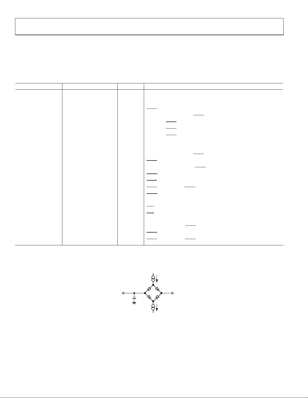
03732-002
Figure 2. Load Circuit for Digital Output Timing
Rev. B | Page 8 of 40
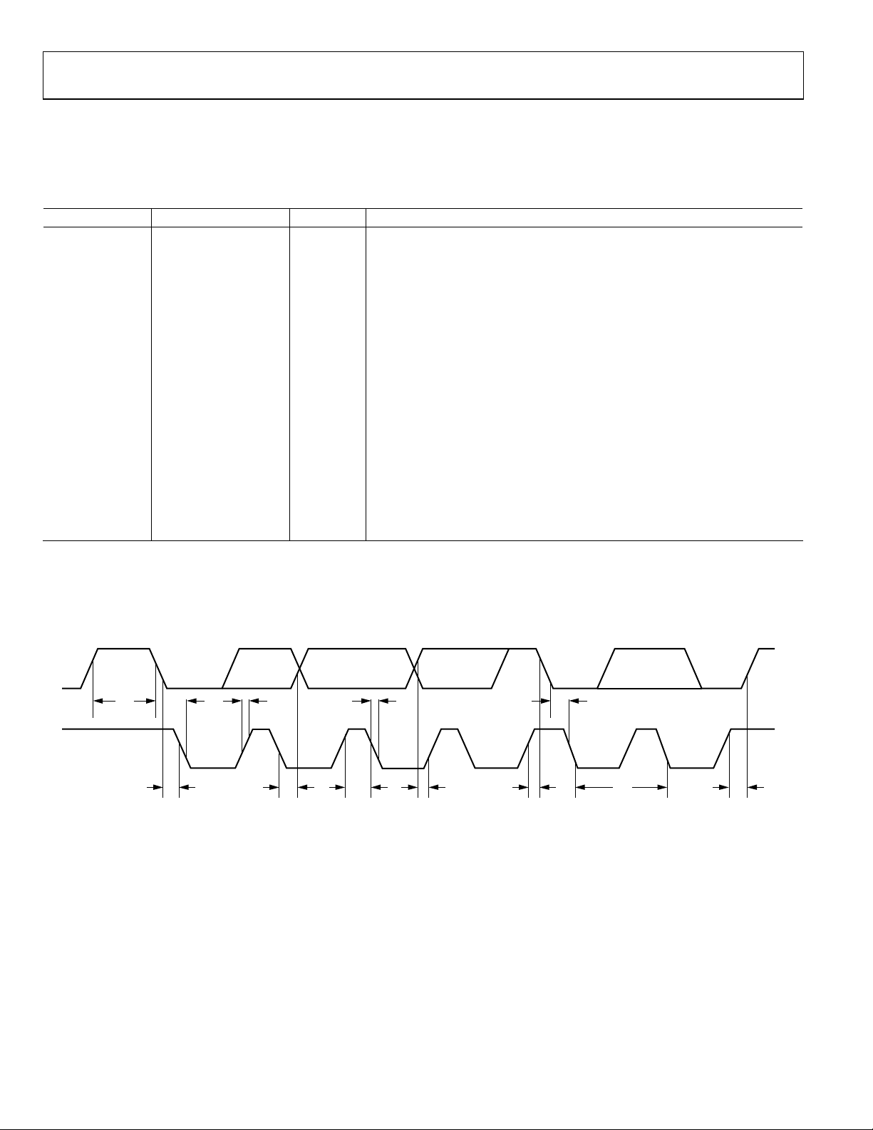
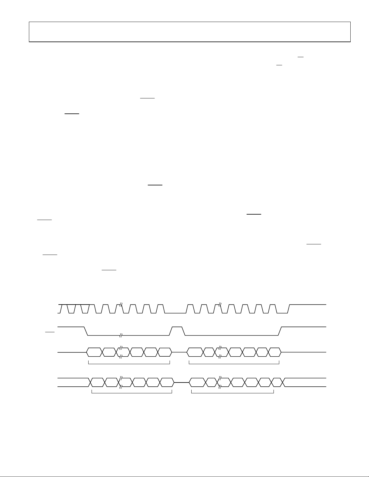
AD5381
t
1
SCLK
SYNC
DIN
BUSY
1
LDAC
VOUT1
2
LDAC
VOUT2
CLR
VOUT
t
7
1
LDAC ACTIVE DURING BUSY.
2
LDAC ACTIVE AFTER BUSY.
Figure 3. Serial Interface Timing Diagram (Standalone Mode)
t
4
DB23
t8t
t
3
t
6
9
t
18
t
2
t
5
DB0
t
10
t
11
t
12
t
19
t
13
t
15
2424
t
17
t
14
t
13
t
17
t
16
03732-003
24 48SCLK
t
7A
SYNC
DIN
SDO
SCLK
SYNC
DIN
SDO
DB23 DB0 DB23 DB0
INPUT WORD SPECIFIES
REGISTER TO BE READ
UNDEFINED
DB23 DB0
NOP CONDITION
SELECTED REGISTER
DATA CLOCKED OUT
Figure 4. Serial Interface Timing Diagram (Data Readback Mode)
t
1
t
t
t
7
t
4
t8t
DB23 DB0 DB0DB23
INPUT WORD FOR DAC N INPUT WORD FOR DAC N + 1
3
9
2
t
20
DB23 DB0
t
03732-004
4824
21
t
22
LDAC
UNDEFINED INPUT WORD FOR DAC N
Figure 5. Serial Interface Timing Diagram (Daisy-Chain Mode)
Rev. B | Page 9 of 40
t
13
t
23
03732-005
AD5381
I2C SERIAL INTERFACE TIMING
DVDD = 2.7 V to 5.5 V; AVDD = 4.5 V to 5.5 V or 2.7 V to 3.6 V; AGND = DGND = 0 V; all specifications T
unless otherwise noted.
MIN
to T
MAX
,
Table 7.
Parameter
F
SCL
t
1
t
2
t
3
t
4
t
5
3
t
6
0 μs min t
t7 0.6 μs min t
t8 0.6 μs min t
t9 1.3 μs min t
1, 2
Limit at T
MIN
, T
Unit Description
MAX
400 kHz max SCL clock frequency
2.5 μs min SCL cycle time
0.6 μs min t
1.3 μs min t
0.6 μs min t
100 ns min t
0.9 μs max t
, SCL high time
HIGH
, SCL low time
LOW
, start/repeated start condition hold time
HD,STA
, data setup time
SU,DAT
, data hold time
HD,DAT
, data hold time
HD,DAT
, setup time for repeated start
SU,STA
, stop condition setup time
SU,STO
, bus free time between a STOP and a START condition
BUF
t10 300 ns max tR, rise time of SCL and SDA when receiving
0 ns min tR, rise time of SCL and SDA when receiving (CMOS compatible)
t11 300 ns max tF, fall time of SDA when transmitting
0 ns min tF, fall time of SDA when receiving (CMOS compatible)
300 ns max tF, fall time of SCL and SDA when receiving
20 + 0.1 C
4
b
ns min tF, fall time of SCL and SDA when transmitting
Cb 400 pF max Capacitive load for each bus line
1
Guaranteed by design and characterization, not production tested.
2
See Figure 6.
3
A master device must provide a hold time of at least 300 ns for the SDA signal (referred to the V
SCL’s falling edge.
4
Cb is the total capacitance, in pF, of one bus line. tR and tF are measured between 0.3 DVDD and 0.7 DVDD.
min of the SCL signal) in order to bridge the undefined region of
IH
SDA
SCL
t
9
t
START
CONDITION
t
3
4
t
10
t
6
t
t
11
2
t
5
REPEATED
CONDITION
t
7
START
t
4
t
1
t
8
STOP
CONDITION
03732-006
Figure 6. I2C-Compatible Serial Interface Timing Diagram
Rev. B | Page 10 of 40
AD5381
PARALLEL INTERFACE TIMING
DVDD = 2.7 V to 5.5 V; AVDD = 4.5 V to 5.5 V or 2.7 V to 3.6 V; AGND = DGND = 0 V; all specifications T
unless otherwise noted.
MIN
to T
MAX
,
Table 8.
Parameter
t0 4.5 ns min
t1 4.5 ns min
t2 20 ns min
t3 20 ns min
t4 0 ns min
t5 0 ns min
t6 4.5 ns min
t7 4.5 ns min
t
8
4
t
700 ns min
9
4
t
30 ns max
10
4, 5
t
11
t
12
t13 20 ns min
t
14
t15 20 ns min
t16 0 ns min
t
17
1, ,2 3
Limit at T
MIN
, T
MAX
Unit Description
20 ns min
670 ns max
30 ns min
100 ns max
100 ns min
REG0, REG1, address to
REG0, REG1, address to
WR rising edge setup time
WR rising edge hold time
CS pulse width low
WR pulse width low
CS to WR falling edge setup time
WR to CS rising edge hold time
WR rising edge setup time
Data to
WR rising edge hold time
Data to
WR pulse width high
Minimum
WR cycle time (single-channel write)
WR rising edge to BUSY falling edge
BUSY pulse width low (single-channel update)
WR rising edge to LDAC falling edge
LDAC pulse width low
BUSY rising edge to DAC output response time
LDAC rising edge to WR rising edge
BUSY rising edge to LDAC falling edge
LDAC falling edge to DAC output response time
t18 8 μs typ DAC output settling time, boost mode off
t19 20 ns min
t20 12 μsmax
1
Guaranteed by design and characterization, not production tested.
2
All input signals are specified with tR = tR = 5 ns (10% to 90% of DVDD) and timed from a voltage level of 1.2 V.
3
See Figure 7.
4
See Figure 29.
5
Measured with the load circuit of Figure 2.
CLR pulse width low
CLR pulse activation time
Rev. B | Page 11 of 40
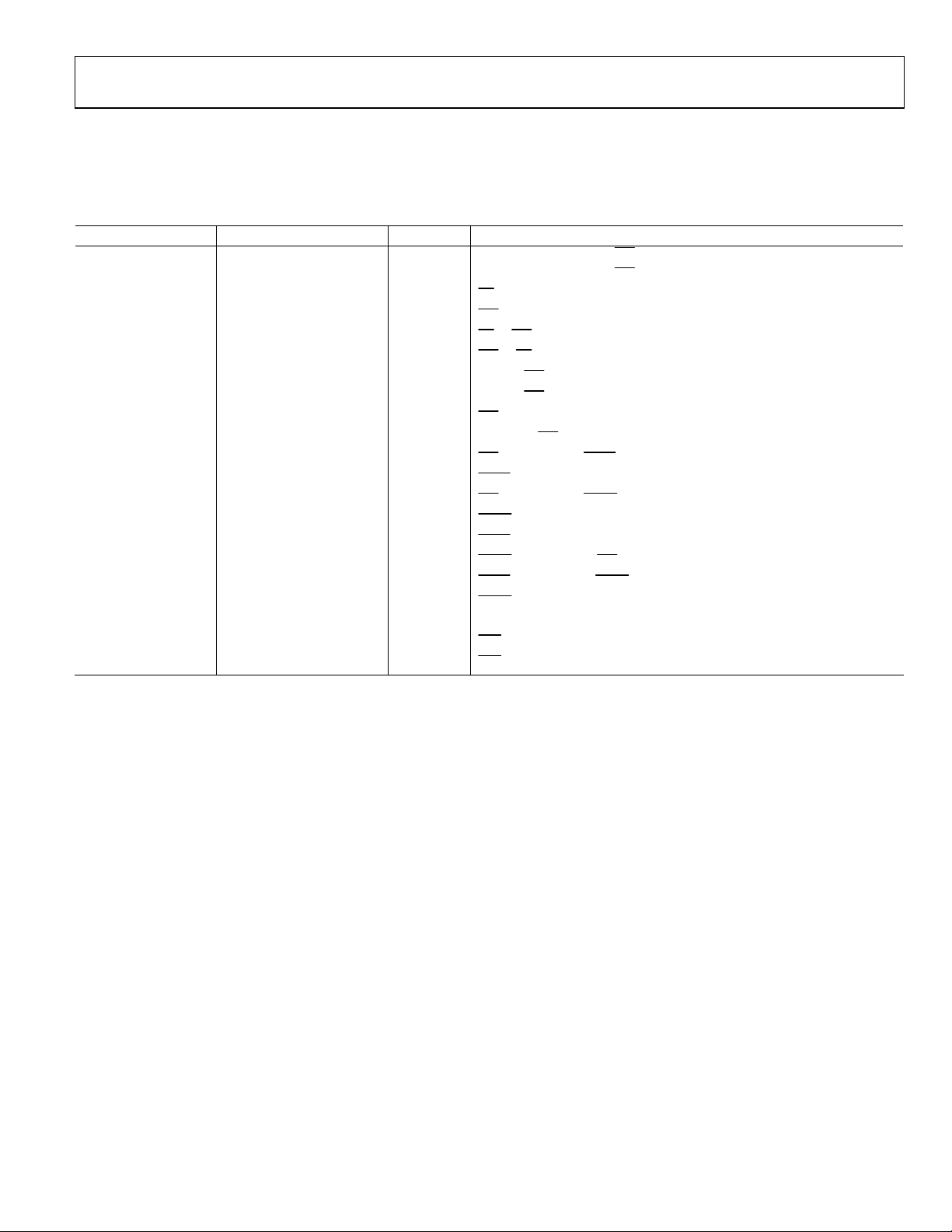
AD5381
t
t
0
1
REG0, REG1, A5...A0
CS
WR
DB11...DB0
BUSY
LDAC
VOUT1
LDAC
VOUT2
CLR
VOUT
1
2
t
4
t
5
t
2
t
9
t
3
t
6
t
t
t
8
t
t
7
10
t
11
t
12
19
t
13
t
20
15
t
18
t
14
t
16
t
13
t
18
t
17
1
LDAC ACTIVE DURING BUSY.
2
LDAC ACTIVE AFTER BUSY.
03732-007
Figure 7. Parallel Interface Timing Diagram
Rev. B | Page 12 of 40

AD5381
ABSOLUTE MAXIMUM RATINGS
TA = 25°C, unless otherwise noted.
Table 9.
Parameter Rating
AVDD to AGND –0.3 V to +7 V
DVDD to DGND –0.3 V to +7 V
Digital Inputs to DGND –0.3 V to DVDD + 0.3 V
SDA/SCL to DGND –0.3 V to +7 V
Digital Outputs to DGND –0.3 V to DVDD + 0.3 V
REFIN/REFOUT to AGND –0.3 V to AVDD + 0.3 V
AGND to DGND –0.3 V to +0.3 V
VOUTx to AGND –0.3 V to AVDD + 0.3 V
Analog Inputs to AGND –0.3 V to AVDD + 0.3 V
Operating Temperature Range
Commercial (B Version) –40°C to +85°C
Storage Temperature Range –65°C to +150°C
JunctionTemperature (TJ
100-Lead LQFP Package
θJAThermal Impedance 44°C/W
Reflow Soldering
Peak Temperature 230°C
Reflow Soldering (Pb-free)
Peak Temperature 260(0/-5)°C
Time at Peak Temperature 10 sec to 40 sec
1
Transient currents of up to 100 mA will not cause SCR latch-up.
MAX
1
) 150°C
Stresses above those listed under Absolute Maximum Ratings
may cause permanent damage to the device. This is a stress
rating only; functional operation of the device at these or any
other conditions above those listed in the operational sections
of this specification is not implied. Exposure to absolute maximum rating conditions for extended periods may affect device
reliability.
ESD CAUTION
ESD (electrostatic discharge) sensitive device. Electrostatic charges as high as 4000 V readily
accumulate on the human body and test equipment and can discharge without detection. Although
this product features proprietary ESD protection circuitry, permanent damage may occur on devices
subjected to high energy electrostatic discharges. Therefore, proper ESD precautions are
recommended to avoid performance degradation or loss of functionality.
Rev. B | Page 13 of 40

AD5381
PIN CONFIGURATION AND FUNCTION DESCRIPTIONS
C)
2
CS/(SYNC/AD0)
DB11/(DIN/SDA)
DB10/(SCLK/SCL)
DB9/(SPI/I
DB8
DB7
DB6
SDO/(A/B)
DVDD
DGND
FIFO EN
CLR
VOUT24
VOUT25
VOUT26
VOUT27
SIGNAL_GND4
DAC_GND4
AGND4
AVDD4
VOUT28
VOUT29
VOUT30
VOUT31
REFGND
REFOUT/REFIN
SIGNAL_GND1
DAC_GND1
AVDD1
VOUT0
VOUT1
VOUT2
VOUT3
VOUT4
AGND1
DGNDA5A4A3A2A1A0
9899979695949291908988
100
1
PIN 1
2
IDENTIFIER
3
4
5
6
7
8
9
10
11
12
13
14
15
16
17
18
19
20
21
22
23
24
25
8793868584828180797877
AD5381
TOP VIEW
(Not to Scale)
DVDD
83
DVDD
DGND
SER/PARPDWR (DCEN/AD1)
LDAC
BUSY
76
75
RESET
74
DB5
73
DB4
72
DB3
71
DB2
70
DB1
69
DB0
68
NC
67
NC
66
REG0
65
REG1
64
VOUT23
63
VOUT22
62
VOUT21
61
VOUT20
60
AVDD3
59
AGND3
58
DAC_GND3
57
SIGNAL_GND3
56
VOUT19
55
VOUT18
54
VOUT17
53
VOUT16
52
AVDD2
51
AGND2
262827293032333435
VOUT5
AVDD5
AGND5
DAC_GND5
SIGNAL_GND5
NC = NO CONNECT
VOUT6
VOUT7
363137383940424344
VOUT32
VOUT33
VOUT34
VOUT35
VOUT36
VOUT37
VOUT38
Figure 8. 100-Lead LQFP Pin Configuration
Table 10. Pin Function Descriptions
Mnemonic Function
VOUTx
Buffered Analog Outputs for Channel x. Each analog output is driven by a rail-to-rail output amplifier operating at a
gain of 2. Each output is capable of driving an output load of 5 kΩ to ground. Typical output impedance is 0.5 Ω.
SIGNAL_GND(1–5)
Analog Ground Reference Points for Each Group of Eight Output Channels. All SIGNAL_GND pins are tied together
internally and should be connected to the AGND plane as close as possible to the AD5381.
DAC_GND(1–5)
Each group of eight channels contains a DAC_GND pin. This is the ground reference point for the internal 12-bit DAC.
These pins shound be connected to the AGND plane.
AGND(1–5)
Analog Ground Reference Point. Each group of eight channels contains an AGND pin. All AGND pins should be
connected externally to the AGND plane.
AVDD(1–5)
Analog Supply Pins. Each group of eight channels has a separate AVDD pin. These pins are shorted internally and
should be decoupled with a 0.1 μF ceramic capacitor and 10 μF tantalum capacitor. Operating range for the
AD5381-5 is 4.5 V to 5.5 V; operating range for the AD5381-3 is 2.7 V to 3.6 V.
DGND Ground for All Digital Circuitry.
DVDD
Logic Power Supply. Guaranteed operating range is 2.7 V to 5.5 V. It is recommended that these pins be decoupled
with a 0.1 μF ceramic and a 10 μF tantalum capacitors to DGND.
REFGND Ground Reference Point for the Internal Reference.
VOUT39/MON_OUT
45414647484950
VOUT8
VOUT9
VOUT10
VOUT11
VOUT12
DAC_GND2
SIGNAL_GND2
VOUT13
VOUT14
VOUT15
03732-008
Rev. B | Page 14 of 40

AD5381
Mnemonic Function
REFOUT/REFIN
VOUT39/MON_OUT
SER/PAR Interface Select Input. This pin allows the user to select whether the serial or parallel interface is used. If it is tied high,
CS/(SYNC/AD0) In parallel interface mode, this pin acts as chip select input (level sensitive, active low). When low, the AD5381
Serial Interface Mode. This is the frame synchronization input signal for the serial clock and data.
WR/(DCEN/AD1) Multifunction Pin. In parallel interface mode, this pin acts as write enable. In serial interface mode, this pin acts as a
DB11–DB0 Parallel Data Bus. DB11 is the MSB and DB0 is the LSB of the input data-word on the AD5381.
A5–A0
REG1, REG0
SDO/(A/B) Serial Data Output in Serial Interface Mode. Three-stateable CMOS output. SDO can be used for daisy-chaining a
BUSY Digital CMOS Output. BUSY goes low during internal calculations of the data (x2) loaded to the DAC data register.
LDAC Load DAC Logic Input (Active Low). If LDAC is taken low while BUSY is inactive (high), the contents of the input
CLR Asynchronous Clear Input. The CLR input is falling edge sensitive. When CLR is activated, all channels are updated
RESET Asynchronous Digital Reset Input (Falling Edge Sensitive). The function of this pin is equivalent to that of the power-
The AD5381 contains a common REFOUT/REFIN pin. When the internal reference is selected, this pin is the reference
output. If the application requires an external reference, it can be applied to this pin and the internal reference can
be disabled via the control register. The default for this pin is a reference input.
This pin has a dual function. It acts as a buffered output for Channel 39 in default mode. However, when the monitor
function is enabled, this pin acts as the output of a 39-to-1 channel multiplexer that can be programmed to
multiplex one of Channels 0 to 38 to the MON_OUT pin. The MON_OUT pin’s output impedance is typically 500 Ω
and is intended to drive a high input impedance like that exhibited by SAR ADC inputs.
the serial interface mode is selected and Pin 97 (
SPI/I2C) is used to determine if the interface mode is SPI or I2C.
Parallel interface mode is selected when SER/PAR is low.
is selected.
2
C Mode. This pin acts as a hardware address pin used in conjunction with AD1 to determine the software address
I
for the device on the I
daisy-chain enable in SPI mode and as a hardware address pin in I
Parallel Interface Write Input (edge sensitive). The rising edge of
2
C bus.
2
C mode.
WR is used in conjunction with CS low, and the
address bus inputs to write to the selected device registers.
Serial Interface. Daisy-chain select input (level sensitive, active high). When high, this signal is used in conjunction
with SER/
2
C Mode. This pin acts as a hardware address pin used in conjunction with AD0 to determine the software address
I
for this device on the I
PAR high to enable the SPI serial interface daisy-chain mode.
2
C bus.
Parallel Address Inputs. A5 to A0 are decoded to address one of the AD5381’s 40 input channels. Used in conjunction
with the REG1 and REG0 pins to determine the destination register for the input data.
In parallel interface mode, REG1 and REG0 are used in decoding the destination registers for the input data. REG1
and REG0 are decoded to address the input data register, offset register, or gain register for the selected channel and
are also used to decide the special function registers.
number of devices together. Data is clocked out on SDO on the rising edge of SCLK, and is valid on the falling edge
of SCLK.
When operating in parallel interface mode, this pin acts as the A or B data register select when writing data to the
AD5381’s data registers with toggle mode selected (see the Toggle Mode Function section). In toggle mode, the
LDAC is used to switch the output between the data contained in the A and B data registers. All DAC channels
contain two data registers. In normal mode, Data Register A is the default for data transfers.
During this time, the user can continue writing new data to the x1, c, and m registers, but no further updates to the
DAC registers and DAC outputs can take place. If
goes low during power-on reset, and when the
events on
LDAC are ignored. A CLR operation also brings BUSY low.
registers are transferred to the DAC registers and the DAC outputs are updated. If
LDAC is taken low while BUSY is low, this event is stored. BUSY also
RESET pin is low. During this time, the interface is disabled and any
LDAC is taken low while BUSY is
active and internal calculations are taking place, the LDAC event is stored and the DAC registers are updated when
BUSY goes inactive. However any events on LDAC during power-on reset or on RESET are ignored.
with the data contained in the
updated with the
CLR code.
CLR code register. BUSY is low for a duration of 35 μs while all channels are being
on reset generator. When this pin is taken low, the state machine initiates a reset sequence to digitally reset the x1,
m, c, and x2 registers to their default power-on values. This sequence typically takes 270 μs. The falling edge of
RESET
initiates the RESET process and BUSY goes low for the duration, returning high when RESET is complete. While BUSY
is low, all interfaces are disabled and all
operation and the status of the
RESET pin is ignored until the next falling edge is detected.
LDAC pulses are ignored. When BUSY returns high, the part resumes normal
Rev. B | Page 15 of 40

AD5381
Mnemonic Function
PD
FIFO EN
DB9/(SPI/I2C) Multifunction Input Pin. In parallel interface mode, this pin acts as DB9 of the parallel input data-word. In serial
In this mode, DB12 is the serial clock (SCL) input and DB11 is the serial data (SDA) input.
DB10/(SCLK/SCL)
DB11/(DIN/SDA) Multifunction Data Input Pin. In parallel interface mode, this pin acts as DB11 of the parallel input data-word.
I
Power-Down (Level Sensitive, Active High). PD is used to place the device in low power mode, where the analog
current consumption is reduced to 2 μA and the digital current consumption is reduced to 20 μA. In power-down
mode, all internal analog circuitry is placed in low power mode, and the analog output is configured as a high
impedance output or provides a 100 kΩ load to ground, depending on how the power-down mode is configured.
The serial interface remains active during power-down.
FIFO Enable (Level Sensitive, Active High). When connected to DVDD, the internal FIFO is enabled, allowing the user
to write to the device at full speed. FIFO is only available in parallel interface mode. The status of the FIFO EN pin is
sampled on power-up, and also following a CLEAR or RESET, to determine if the FIFO is enabled. In either serial or
2
I
C interface modes, the FIFO EN pin should be tied low.
interface mode, this pin acts as serial interface mode select. When serial interface mode is selected (SER/PAR = 1) and
this input is low, SPI mode is selected. In SPI mode, DB12 is the serial clock (SCLK) input and DB11 is the serial data
(DIN) input.
When serial interface mode is selected (SER/
PAR = 1) and this input is high I2C Mode is selected.
Multifunction Input Pin. In parallel interface mode, this pin acts as DB10 of the parallel input data-word. In serial
interface mode, this pin acts as a serial clock input.
Serial Interface Mode. In serial interface mode, data is clocked into the shift register on the falling edge of SCLK.
This operates at clock speeds up to 50 MHz.
2
C Mode. In I2C mode, this pin performs the SCL function, clocking data into the device. The data transfer rate in
I
2
C mode is compatible with both 100 kHz and 400 kHz operating modes.
I
Serial Interface Mode. In serial interface mode, this pin acts as the serial data input. Data must be valid on the falling
edge of SCLK.
2
C Mode. In I2C mode, this pin is the serial data pin (SDA) operating as an open-drain input/output.
Rev. B | Page 16 of 40

AD5381
TERMINOLOGY
Relative Accuracy
Relative accuracy, or endpoint linearity, is a measure of the
maximum deviation from a straight line passing through the
endpoints of the DAC transfer function. It is measured after
adjusting for zero-scale error and full-scale error, and is
expressed in LSB.
Differential Nonlinearity
Differential nonlinearity is the difference between the measured
change and the ideal 1 LSB change between any two adjacent
codes. A specified differential nonlinearity of 1 LSB maximum
ensures monotonicity.
Zero-Scale Error
Zero-scale error is the error in the DAC output voltage when all
0s are loaded into the DAC register. Ideally, with all 0s loaded
to the DAC and m = all 1s, c = 2
VOUT
Zero-scale error is a measure of the difference between VOUT
(actual) and VOUT (ideal), expressed in mV. It is mainly due to
offsets in the output amplifier.
Offset Error
Offset error is a measure of the difference between VOUT
(actual) and VOUT (ideal) in the linear region of the transfer
function, expressed in mV. Offset error is measured on the
AD5381-5 with Code 32 loaded into the DAC register, and on
the AD5381-3 with Code 64.
Gain Error
Gain Error is specified in the linear region of the output range
between VOUT = 10 mV and VOUT = AVDD – 50 mV. It is
the deviation in slope of the DAC transfer characteristic from
the ideal and is expressed in %FSR with the DAC output
unloaded.
DC Crosstalk
This is the dc change in the output level of one DAC at
midscale in response to a full-scale code (all 0s to all 1s, and
vice versa) and output change of all other DACs. It is expressed
in LSB.
(Zero-Scale)
= 0 V
n – 1
DC Output Impedance
This is the effective output source resistance. It is dominated by
package lead resistance.
Output Voltage Settling Time
This is the amount of time it takes for the output of a DAC to
settle to a specified level for a ¼ to ¾ full-scale input change,
and is measured from the
Digital-to-Analog Glitch Energy
This is the amount of energy injected into the analog output at
the major code transition. It is specified as the area of the glitch
in nV-s. It is measured by toggling the DAC register data
between 0x7FF and 0x800.
DAC-to-DAC Crosstalk
DAC-to-DAC crosstalk is the glitch impulse that appears at the
output of one DAC due to both the digital change and the
subsequent analog output change at another DAC. The victim
channel is loaded with midscale. DAC-to-DAC crosstalk is
specified in nV-s.
Digital Crosstalk
The glitch impulse transferred to the output of one converter
due to a change in the DAC register code of another converter
is defined as the digital crosstalk and is specified in nV-s.
Digital Feedthrough
When the device is not selected, high frequency logic activity
on the device’s digital inputs can be capacitively coupled both
across and through the device to show up as noise on the
VOUT pins. It can also be coupled along the supply and
ground lines. This noise is digital feedthrough.
Output Noise Spectral Density
This is a measure of internally generated random noise.
Random noise is characterized as a spectral density (voltage per
√Hertz). It is measured by loading all DACs to midscale and
measuring noise at the output. It is measured in nV/√Hz in a
1 Hz bandwidth at 10 kHz.
BUSY
rising edge.
Rev. B | Page 17 of 40
AD5381
TYPICAL PERFORMANCE CHARACTERISTICS
1.00
0.75
0.50
AVDD = 5V
REFIN = 2.5V
T
= 25°C
A
1.00
0.75
0.50
AVDD = 3V
REFIN = 1.25V
= 25°C
T
A
INL ERROR (LSB)
AMPLITUDE (V)
0.25
–0.25
–0.50
–0.75
–1.00
2.539
2.538
2.537
2.536
2.535
2.534
2.533
2.532
2.531
2.530
2.529
2.528
2.527
2.526
2.525
2.524
2.523
0.25
–0.25
INL ERROR (LSB)
–0.50
–0.75
–1.00
1.254
1.253
1.252
1.251
1.250
1.249
1.248
AMPLITUDE (V)
1.247
1.246
1.245
0
INPUT CODE
40960 512 1024 1536 2048 2560 3072 3584
03732-012
Figure 12. Typical AD5381-3 INL Plot
AVDD = DVDD = 3V
= 1.25V
V
REF
= 25°C
T
A
14ns/SAMPLE NUMBER
1 LSB CHANGE AROUND MIDSCALE
GLITCH IMPULSE = 5nV-s
SAMPLE NUMBER
5500 100 150 200 250 30050 350 400 500450
03732-013
Figure 13. AD5381-3 Glitch Impulse
0
INPUT CODE
40960 512 1024 1536 2048 2560 3072 3584
03732-009
Figure 9. Typical AD5381-5 INL Plot
AVDD = DVDD = 5V
V
= 2.5V
REF
T
= 25°C
A
14ns/SAMPLE NUMBER
1 LSB CHANGE AROUND MIDSCALE
GLITCH IMPULSE = 10nV-s
SAMPLE NUMBER
5500 100 150 200 250 30050 350 400 500450
03732-010
Figure 10. AD5381-5 Glitch Impulse
AVDD = DVDD = 5V
= 2.5V
V
REF
= 25°C
T
A
VOUT
Figure 11. Slew Rate with Boost Off
03732-011
Rev. B | Page 18 of 40
AVDD = DVDD = 5V
V
= 2.5V
REF
T
= 25°C
A
Figure 14. Slew Rate with Boost On
VOUT
03732-014

AD5381
PERCENTAGE OF UNITS (%)
14
12
10
8
6
4
2
10
8
6
Figure 15. AI
AIDD (mA)
Histogram with Boost Off
DD
AVDD = 5.5V
V
= 2.5V
REF
= 25°C
T
A
118910
DVDD = 5.5V
= DVDD
V
IH
= DGND
V
IL
T
= 25°C
A
03732-015
AVDD = DVDD = 5V
V
= 2.5V
REF
T
= 25°C
A
POWER SUPPLY RAMP RATE = 10ms
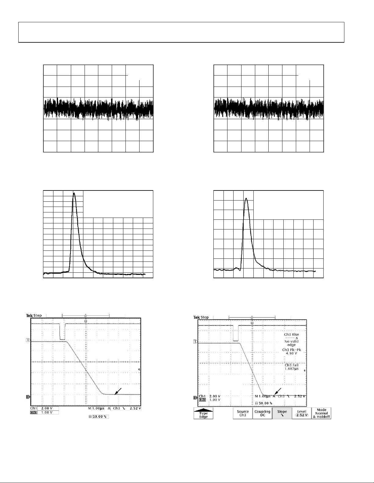
Figure 18. Power-Up Transient
40
35
30
25
20
VOUT
AVDD
03732-018
4
NUMBER OF UNITS
2
0
WR
AVDD = DVDD = 5V
= 2.5V
V
REF
= 25°C
T
A
EXITS SOFT PD
TO MIDSCALE
0.8 0.90.4 0.5 0.6 0.7
Figure 16. DI
DIDD (mA)
Histogram
DD
BUSY
VOUT
Figure 17. Exiting Soft Power-Down
03732-017
03732-016
FREQUENCY
15
10
5
0
–5.0
–4.0
–1.0 3.0–3.0 1.00 4.0 5.0
–2.0 2.0
–1.5 2.5–3.5–4.5
REFERENCE DRIFT (ppm/°C)
0.5–0.5 3.5–2.5 1.5
Figure 19. REFOUT Temperature Coefficient
PD
VOUT
Figure 20. Exiting Hardware Power-Down
4.5
AVDD = DVDD = 5V
V
= 2.5V
REF
T
= 25°C
EXITS HARDWARE PD
A
TO MIDSCALE
03732-020
03732-019
Rev. B | Page 19 of 40

AD5381
6
FULL SCALE
5
4
3
3/4 SCALE
MIDSCALE
AVDD = DVDD= 5V
V
= 2.5V
REF
= 25°C
T
A
6
AVDD = DVDD = 3V
= 1.25V
V
REF
= 25°C
T
A
5
4
3
MIDSCALE
3/4 SCALE
FULL SCALE
2
VOUT (V)
1
0
–1
–40 –20 –10 –5 –2 0 2 5 10 20 40
1/4 SCALE
ZERO SCALE
CURRENT (mA)
Figure 21. AD5381-5 Output Amplifier Source and Sink Capability
ERROR VOLTAGE (V)
0.20
0.15
0.10
0.05
–0.05
–0.10
–0.15
–0.20
ERROR AT ZERO SINKING CURRENT
0
(VDD–VOUT) AT FULL-SCALE SOURCING CURRENT
I
SOURCE/ISINK
(mA)
AVDD = 5V
= 2.5V
V
REF
T
= 25°C
A
2.000 0.25 0.50 0.75 1.00 1.25 1.50 1.75
Figure 22. Headroom at Rails vs. Source/Sink Current
600
500
400
300
AVDD = 5V
= 25°C
T
A
REFOUT DECOUPLED
WITH 100nF CAPACITOR
03732-021
03732-022
2
VOUT (V)
1
0
–1
–40 –20 –10 –5 –2 0 2 5 10 20 –40
ZERO SCALE
1/4 SCALE
CURRENT (mA)
Figure 24. AD5381-3 Output Amplifier Source and Sink Capability
2.456
2.455
2.454
2.453
2.452
AMPLITUDE (V)
2.451
2.450
2.449
SAMPLE NUMBER
AVDD = DVDD = 5V
= 2.5V
V
REF
= 25°C
T
A
14ns/SAMPLE NUMBER
5500 100 150 200 250 30050 350 400 500450
Figure 25. Adjacent Channel DAC-to-DAC Crosstalk
AVDD = DVDD = 5V
T
= 25°C
A
DAC LOADED WITH MIDSCALE
EXTERNAL REFERENCE
Y AXIS = 5μV/DIV
X AXIS = 100ms/DIV
03732-024
03732-025
REFOUT = 2.5V
FREQUENCY (Hz)
AVDD = DVDD = 5V
V
= 2.5V
REF
T
= 25°C
A
EXITS SOFT PD
100k100 1k 10k
03732-023
TO MIDSCALE
03732-026
Figure 26. 0.1 Hz to 10 Hz Noise Plot
OUTPUT NOISE (nV/ Hz)
200
100
0
REFOUT = 1.25V
Figure 23. REFOUT Noise Spectral Density
Rev. B | Page 20 of 40

AD5381
A
FUNCTIONAL DESCRIPTION
DAC ARCHITECTURE—GENERAL
The AD5381 is a complete, single-supply, 40-channel voltage
output DAC that offers 12-bit resolution. The part is available
in a 100-lead LQFP package and features both a parallel and
a serial interface. This product includes an internal, software
selectable, 1.25 V/2.5 V, 10 ppm/°C reference that can be used
to drive the buffered reference inputs; alternatively, an external
reference can be used to drive these inputs. Internal/external
reference selection is via the CR8 bit in the control register;
CR10 selects the reference magnitude if the internal reference
is selected. All channels have an on-chip output amplifier with
rail-to-rail output capable of driving 5 kΩ in parallel with a
200 pF load.
VREF AVDD
×1 INPUT
REG
m REG
c REG
Figure 27. Single-Channel Architecture
DAC
×2INPUT DAT
REG
The architecture of a single DAC channel consists of a 12-bit
resistor-string DAC followed by an output buffer amplifier
operating at a gain of 2. This resistor-string architecture
guarantees DAC monotonicity. The 12-bit binary digital code
loaded to the DAC register determines at what node on the
string the voltage is tapped off before being fed to the output
amplifier. Each channel on these devices contains independent
offset and gain control registers that allow the user to digitally
trim offset and gain. These registers give the user the ability to
calibrate out errors in the complete signal chain, including the
DAC, using the internal m and c registers, which hold the
correction factors. All channels are double buffered, allowing synchronous updating of all channels using the
Figure 27 shows a block diagram of a single channel on the
AD5381. The digital input transfer function for each DAC
can be represented as
n
x2 = [(m + 2)/ 2
× x1] + (c – 2
where:
x2 = the data-word loaded to the resistor string DAC.
x1 = the 12-bit data-word written to the DAC input register.
m = the gain coefficient (default is 0xFFE). The gain coefficient
is written to the 11 most significant bits (DB11 to DB1), the LSB
(DB0) of the data-word is a 0.
n = DAC resolution (n = 12 for AD5381).
c = the12-bit offset coefficient (default is 0x800).
12-BIT
DAC
n – 1
VOUT
R
R
03732-027
pin.
LDAC
)
The complete transfer function for these devices can be
represented as
n
VOUT = 2 × V
× x2/2
REF
where:
x2 is the data-word loaded to the resistor string DAC. V
REF
is externally applied to the DAC REFOUT/REFIN pin. For
specified performance, an external reference voltage of 2.5 V is
recommended for the AD5381-5, and 1.25 V for the AD5381-3.
DATA DECODING
The AD5381 contains a 12-bit data bus, DB11 to DB0. Depending on the value of REG1 and REG0 (see
loaded into the addressed DAC input registers, offset (c)
registers, or gain (m) registers. The format data, offset (c), and
gain (m) register contents are shown in
Table 11. Register Selection
REG1 REG0 Register Selected
1 1 Input Data Register (x1)
1 0 Offset Register (c)
0 1 Gain Register (m)
0 0 Special Function Registers (SFRs)
Table 12. DAC Data Format (REG1 = 1, REG0 = 1)
DB11 to DB0 DAC Output (V)
1111 1111 1111 2 V
1111 1111 1110 2 V
1000 0000 0001 2 V
1000 0000 0000 2 V
0111 1111 1111 2 V
0000 0000 0001 2 V
0000 0000 0000 0
Table 13. Offset Data Format (REG1 = 1, REG0 = 0)
DB11 to DB0 Offset (LSB)
1111 1111 1111 +2048
1111 1111 1110 +2047
1000 0000 0001 +1
1000 0000 0000 0
0111 1111 1111 –1
0000 0000 0001 –2047
0000 0000 0000 –2048
Table 14. Gain Data Format (REG1 = 0, REG0 = 1)
DB11 to DB0 Gain Factor
1111 1111 1110 1
1011 1111 1110 0.75
0111 1111 1110 0.5
0011 1111 1110 0.25
0000 0000 0000 0
Table 1 1), this data is
Table 1 2 to Ta ble 1 4.
× (4095/4096)
REF
× (4094/4096)
REF
× (2049/4096)
REF
× (2048/4096)
REF
× (2047/4096)
REF
× (1/4096)
REF
Rev. B | Page 21 of 40

AD5381
ON-CHIP SPECIAL FUNCTION REGISTERS (SFR)
The AD5381 contains a number of special function registers
(SFRs), as outlined in
REG1 = REG0 = 0 and are decoded using Address Bits
A5
to A0.
Table 15. SFR Register Functions (REG1 = 0, REG0 = 0)
R/WA5 A4 A3 A2 A1 A0 Function
X 0 0 0 0 0 0 NOP (No Operation)
0 0 0 0 0 0 1 Write CLR Code
0 0 0 0 0 1 0 Soft CLR
0 0 0 1 0 0 0 Soft Power-Down
0 0 0 1 0 0 1 Soft Power-Up
0 0 0 1 1 0 0 Control Register Write
1 0 0 1 1 0 0 Control Register Read
0 0 0 1 0 1 0 Monitor Channel
0 0 0 1 1 1 1 Soft Reset
SFR COMMANDS
NOP (No Operation)
REG1 = REG0 = 0, A5 to A0 = 000000
Performs no operation but is useful in serial readback mode to
clock out data on D
low during a NOP operation.
Table 1 5. SFRs are addressed with
for diagnostic purposes.
OUT
BUSY
pulses
Soft CLR
REG1 = REG0 = 0, A5 to A0 = 000010
DB11 to DB0 = Don’t Care
Executing this instruction performs the CLR, which is functionally the same as that provided by the external
CLR
pin. The
DAC outputs are loaded with the data in the CLR code register.
It takes 35 μs to fully execute the SOFT CLR, as indicated by the
low time.
BUSY
Soft Power-Down
REG1 = REG0 = 0, A5 to A0 = 001000
DB11 to DB0 = Don’t Care
Executing this instruction performs a global power-down
feature that puts all channels into a low power mode that
reduces the analog supply current to 2 μA max and the digital current to 20 μA max. In power-down mode, the output
amplifier can be configured as a high impedance output or
provide a 100 kΩ load to ground. The contents of all internal
registers are retained in power-down mode. No register can be
written to while in power-down.
Soft Power-Up
REG1 = REG0 = 0, A5 to A0 = 001001
DB11 to DB0 = Don’t Care
Write CLR Code
REG1 = REG0 = 0, A5 to A0 = 000001
DB11 to DB0 = Contain the CLR data
Bringing the
line low or exercising the soft clear function
CLR
will load the contents of the DAC registers with the data contained in the user configurable CLR register, and will set
VOUT0 to VOUT39 accordingly. This can be very useful for
setting up a specific output voltage in a clear condition. It is also
beneficial for calibration purposes; the user can load full scale
or zero scale to the clear code register and then issue a hardware or software clear to load this code to all DACs, removing
the need for individual writes to each DAC. Default on powerup is all zeros.
This instruction is used to power up the output amplifiers and
the internal reference. The time to exit power-down is 8 μs.
The hardware power-down and software function are internally
combined in a digital OR function.
Soft RESET
REG1 = REG0 = 0, A5 to A0 = 001111
DB11 to DB0 = Don’t Care
This instruction is used to implement a software reset. All
internal registers are reset to their default values, which correspond to m at full scale and c at zero scale. The contents of the
DAC registers are cleared, setting all analog outputs to 0 V. The
soft reset activation time is 135 μs.
Rev. B | Page 22 of 40

AD5381
Table 16. Control Register Contents
MSB LSB
CR11 CR10 CR9 CR8 CR7 CR6 CR5 CR4 CR3 CR2 CR1 CR0
Control Register Write/Read
REG1 = REG0 = 0, A5 to A0 = 001100, R/W status determines
if the operation is a write (R/
= 0) or a read (R/W = 1). DB11
W
to DB0 contains the control register data.
CR7 = 0: Monitor Disabled (default on power-up). When the
monitor is disabled, the MON_OUT pin assumes its normal
DAC output function.
Control Register Contents
CR11: Power-Down Status. This bit is used to configure the
output amplifier state in power-down.
CR11 = 1. Amplifier output is high impedance (default on
power-up).
CR11 = 0. Amplifier output is 100 kΩ to ground.
CR10: REF Select. This bit selects the operating internal
reference for the AD5381. CR10 is programmed as follows:
CR10 = 1: Internal reference is 2.5 V (AD5381-5 default), the
recommended operating reference for AD5381-5.
CR10 = 0: Internal reference is 1.25 V (AD5381-3 default),
the recommended operating reference for AD5381-3.
CR9: Current Boost Control. This bit is used to boost the
current in the output amplifier, thereby altering its slew rate.
This bit is configured as follows:
CR9 = 1: Boost Mode On. This maximizes the bias current
in the output amplifier, optimizing its slew rate but increasing
the power dissipation.
CR9 = 0: Boost Mode Off (default on power-up). This
reduces the bias current in the output amplifier and reduces
the overall power consumption.
CR8: Internal/External Reference. This bit determines if the
DAC uses its internal reference or an externally applied
reference.
CR8 = 1: Internal Reference Enabled. The reference output
depends on data loaded to CR10.
CR6: Thermal Monitor Function. When enabled, this function
is used to monitor the internal die temperature of the AD5381.
The thermal monitor powers down the output amplifiers when
the temperature exceeds 130°C. This function can be used to
protect the device in cases where power dissipation may be
exceeded if a number of output channels are simultaneously
short-circuited. A soft power-up will re-enable the output
amplifiers if the die temperature has dropped below 130°C.
CR6 = 1: Thermal Monitor Enabled.
CR6 = 0: Thermal Monitor Disabled (default on power-up).
CR5: Don’t Care.
CR4 to CR0: Toggle Function Enable. This function allows the
user to toggle the output between two codes loaded to the A
and B registers for each DAC. Control Register Bits CR4 to CR0
are used to enable individual groups of eight channels for
operation in toggle mode. A Logic 1 written to any bit enables
a group of channels; a Logic 0 disables a group.
LDAC
is used
to toggle between the two registers.
Table 17.
CR Bit Group Channels
CR4 4 32–39
CR3 3 24–31
CR2 2 16–23
CR1 1 8–15
CR0 0 0–7
Channel Monitor Function
REG1 = REG0 = 0, A5 to A0 = 001010
DB11–DB6 = Contain data to address the monitored channel.
CR8 = 0: External Reference Selected (default on power-up).
CR7: Channel Monitor Enable (see
Channel Monitor Function
section).
CR7= 1: Monitor Enabled. This enables the channel monitor
function. After a write to the monitor channel in the SFR
register, the selected channel output is routed to the
MON_OUT pin. VOUT39 operates at the MON_OUT pin.
A channel monitor function is provided on the AD5381. This
feature, which consists of a multiplexer addressed via the interface, allows any channel output to be routed to the MON_OUT
pin for monitoring using an external ADC. In channel monitor
mode, VOUT39 becomes the MON_OUT pin, to which all
monitored pins are routed. The channel monitor function must
be enabled in the control register before any channels are routed
to MON_OUT. On the AD5381, DB11 to DB6 contain the
channel address for the monitored channel. Selecting Channel
Address 63 three-states MON_OUT.
Rev. B | Page 23 of 40

AD5381
Table 18. AD5381 Channel Monitor Decoding
REG1 REG0 A5 A4 A3 A2 A1 A0 DB11 DB10 DB9 DB8 DB8 DB6 DB5–DB0 MON_OUT
0 0 0 0 1 0 1 0 0 0 0 0 0 0 X VOUT0
0 0 0 0 1 0 1 0 0 0 0 0 0 1 X VOUT1
0 0 0 0 1 0 1 0 0 0 0 0 1 0 X VOUT2
0 0 0 0 1 0 1 0 0 0 0 0 1 1 X VOUT3
0 0 0 0 1 0 1 0 0 0 0 1 0 0 X VOUT4
0 0 0 0 1 0 1 0 0 0 0 1 0 1 X VOUT5
0 0 0 0 1 0 1 0 0 0 0 1 1 0 X VOUT6
0 0 0 0 1 0 1 0 0 0 0 1 1 1 X VOUT7
0 0 0 0 1 0 1 0 0 0 1 0 0 0 X VOUT8
0 0 0 0 1 0 1 0 0 0 1 0 0 1 X VOUT9
0 0 0 0 1 0 1 0 0 0 1 0 1 0 X VOUT10
0 0 0 0 1 0 1 0 0 0 1 0 1 1 X VOUT11
0 0 0 0 1 0 1 0 0 0 1 1 0 0 X VOUT12
0 0 0 0 1 0 1 0 0 0 1 1 0 1 X VOUT13
0 0 0 0 1 0 1 0 0 0 1 1 1 0 X VOUT14
0 0 0 0 1 0 1 0 0 0 1 1 1 1 X VOUT15
0 0 0 0 1 0 1 0 0 1 0 0 0 0 X VOUT16
0 0 0 0 1 0 1 0 0 1 0 0 0 1 X VOUT17
0 0 0 0 1 0 1 0 0 1 0 0 1 0 X VOUT18
0 0 0 0 1 0 1 0 0 1 0 0 1 1 X VOUT19
0 0 0 0 1 0 1 0 0 1 0 1 0 0 X VOUT20
0 0 0 0 1 0 1 0 0 1 0 1 0 1 X VOUT21
0 0 0 0 1 0 1 0 0 1 0 1 1 0 X VOUT22
0 0 0 0 1 0 1 0 0 1 0 1 1 1 X VOUT23
0 0 0 0 1 0 1 0 0 1 1 0 0 0 X VOUT24
0 0 0 0 1 0 1 0 0 1 1 0 0 1 X VOUT25
0 0 0 0 1 0 1 0 0 1 1 0 1 0 X VOUT26
0 0 0 0 1 0 1 0 0 1 1 0 1 1 X VOUT27
0 0 0 0 1 0 1 0 0 1 1 1 0 0 X VOUT28
0 0 0 0 1 0 1 0 0 1 1 1 0 1 X VOUT29
0 0 0 0 1 0 1 0 0 1 1 1 1 0 X VOUT30
0 0 0 0 1 0 1 0 0 1 1 1 1 1 X VOUT31
0 0 0 0 1 0 1 0 1 0 0 0 0 0 X VOUT32
0 0 0 0 1 0 1 0 1 0 0 0 0 1 X VOUT33
0 0 0 0 1 0 1 0 1 0 0 0 1 0 X VOUT34
0 0 0 0 1 0 1 0 1 0 0 0 1 1 X VOUT35
0 0 0 0 1 0 1 0 1 0 0 1 0 0 X VOUT36
0 0 0 0 1 0 1 0 1 0 0 1 0 1 X VOUT37
0 0 0 0 1 0 1 0 1 0 0 1 1 0 X VOUT38
0 0 0 0 1 0 1 0 1 0 0 1 1 1 X Undefined
• • • • • • • • • • • • • • • •
• • • • • • • • • • • • • • • •
0 0 0 0 1 0 1 0 1 1 1 1 1 0 X Undefined
0 0 0 0 1 0 1 0 1 1 1 1 1 1 X Three-State
REG1 REG0A5 A4 A3 A2 A1 A0
VOUT0
VOUT1
VOUT37
VOUT38
00001010
AD5381
CHANNEL
MONITOR
DECODING
CHANNEL ADDRESS
DB11–DB6
VOUT39/MON_OUT
Figure 28. Channel Monitor Decoding
Rev. B | Page 24 of 40
03732-028

AD5381
HARDWARE FUNCTIONS
RESET FUNCTION
Bringing the
registers to their power-on reset state. Reset is a negative edge-
sensitive input. The default corresponds to m at full-scale and
to c at zero scale. The contents of the DAC registers are cleared,
setting VOUT0 to VOUT39 to 0 V. This sequence takes 270 μs.
The falling edge of
low for the duration, returning high when
While
BUSY
pulses are ignored. When
normal operation and the status of the
until the next falling edge is detected.
line low resets the contents of all internal
RESET
initiates the reset process;
RESET
RESET
BUSY
is complete.
is low, all interfaces are disabled and all LDAC
returns high, the part resumes
BUSY
pin is ignored
RESET
goes
ASYNCHRONOUS CLEAR FUNCTION
Bringing the
registers to the data contained in the user configurable CLR
register and sets VOUT0 to VOUT39 accordingly. This function can be used in system calibration to load zero-scale and
full-scale to all channels. The execution time for a CLR is 35 μs.
line low clears the contents of the DAC
CLR
FIFO OPERATION IN PARALLEL MODE
The AD5381 contains a FIFO to optimize operation when
operating in parallel interface mode. The FIFO Enable (level
sensitive, active high) is used to enable the internal FIFO. When
connected to DVDD, the internal FIFO is enabled, allowing the
user to write to the device at full speed. FIFO is only available in
parallel interface mode. The status of the FIFO EN pin is sampled on power-up, and after a
the FIFO is enabled. In either serial or I
FIFO EN should be tied low. Up to 128 successive instructions
can be written to the FIFO at maximum speed in parallel mode.
When the FIFO is full, any further writes to the device are
ignored.
Figure 29 shows a comparison between FIFO mode
and non-FIFO mode in terms of channel update time.
also outlines digital loading time.
25
20
or
CLR
WITHOUT FIFO
(CHANNEL UPDATE TIME)
, to determine if
RESET
2
C interface modes,
Figure 29
AND
BUSY
is a digital CMOS output that indicates the status of the
BUSY
FUNCTIONS
LDAC
AD5381. The value of x2, the internal data loaded to the DAC
data register, is calculated each time the user writes new data to
the corresponding x1, c, or m registers. During the calculation
of x2, the
output goes low. While
BUSY
is low, the user
BUSY
can continue writing new data to the x1, m, or c registers, but
no DAC output updates can take place. The DAC outputs are
updated by taking the
is active, the
BUSY
LDAC
update immediately after
the
input permanently low, in which case the DAC
LDAC
outputs update immediately after
LDAC
input low. If
goes low while
LDAC
event is stored and the DAC outputs
goes high. The user may hold
BUSY
goes high.
BUSY
BUSY
also goes low during power-on reset and when a falling edge is
detected on the
disabled and any events on
pin. During this time, all interfaces are
RESET
are ignored.
LDAC
The AD5381 contains an extra feature whereby a DAC register
is not updated unless its x2 register has been written to since
the last time
was brought low. Normally, when
LDAC
LDAC
is brought low, the DAC registers are filled with the contents
of the x2 registers. However, the AD5381 will only update the
DAC register if the x2 data has changed, thereby removing
unnecessary digital crosstalk.
15
s)
μ
10
TIME (
5
(DIGITAL LOADING TIME)
0
1 4 7 10 13 16 19 22 25 28 31 34 37
Figure 29. Channel Update Rate (FIFO vs. NON-FIFO)
NUMBER OF WRITES
WITH FIFO
(CHANNEL UPDATE TIME)
WITH FIFO
40
03732-029
POWER-ON RESET
The AD5381 contains a power-on reset generator and state
machine. The power-on reset resets all registers to a predefined
state and configures the analog outputs as high impedance. The
pin goes low during the power-on reset sequencing, pre-
BUSY
venting data writes to the device.
POWER-DOWN
The AD5381 contains a global power-down feature that puts all
channels into a low power mode and reduces the analog power
consumption to 2 μA max and digital power consumption to
20 μA max. In power-down mode, the output amplifier can be
configured as a high impedance output or can provide a 100 kΩ
load to ground. The contents of all internal registers are retained
in power-down mode. When exiting power-down, the settling
time of the amplifier will elapse before the outputs settle to their
correct values.
Rev. B | Page 25 of 40

AD5381
INTERFACES
The AD5381 contains both parallel and serial interfaces.
Furthermore, the serial interface can be programmed to be
either SPI-, DSP-, MICROWIRE-, or I
SER/
serial mode, the
MICROWIRE-, or I
pin selects parallel and serial interface modes. In
PA R
/I2C pin is used to select DSP-, SPI-,
SPI
2
C-interface mode.
The devices use an internal FIFO memory to allow high speed
successive writes in parallel interface mode. The user can continue writing new data to the device while write instructions are
being executed. The
signal indicates the current status of
BUSY
the device, going low while instructions in the FIFO are being
executed. In parallel mode, up to 128 successive instructions
can be written to the FIFO at maximum speed. When the FIFO
is full, any further writes to the device are ignored.
To minimize both the power consumption of the device and the
on-chip digital noise, the active interface only powers up fully
when the device is being written to, that is, on the falling edge
of
or the falling edge of
WR
SYNC
DSP-, SPI-, MICROWIRE-COMPATIBLE SERIAL INTERFACES
The serial interface can be operated with a minimum of three
wires in standalone mode or four wires in daisy-chain mode.
Daisy chaining allows many devices to be cascaded together to
increase system channel count. The SER/
high and the
the DSP-/SPI-/MICROWIRE-compatible serial interface. In
serial interface mode, the user does not need to drive the parallel input data pins. The serial interface’s control pins are
/I2C pin (Pin 97) should be tied low to enable
SPI
2
C-compatible. The
.
pin must be tied
PA R
Figure 3 and Figure 5 show timing diagrams for a serial write
to the AD5381 in standalone and daisy-chain modes. The 24-bit
data-word format for the serial interface is shown in
/B This pin selects whether the data write is to the A or B
A
Table 1 9.
register when toggle mode is enabled. With toggle disabled, this
bit should be set to 0 to select the A data register.
is the read or write control bit.
R/
W
A5 to A0 are used to address the input channels.
REG1 and REG0 select the register to which data is written,
as shown in
Table 11.
DB11 to .DB0 contain the input data-word.
X is a don’t care condition.
Standalone Mode
By connecting the DCEN (daisy-chain enable) pin low, standalone mode is enabled. The serial interface works with both a
continuous and a noncontinuous serial clock. The first falling
edge of
starts the write cycle and resets a counter that
SYNC
counts the number of serial clocks to ensure the correct number
of bits are shifted into the serial shift register. Any further edges
on
, except for a falling edge, are ignored until 24 bits are
SYNC
clocked in. Once 24 bits are shifted in, the SCLK is ignored. In
order for another serial transfer to take place, the counter must
be reset by the falling edge of
SYNC
.
, DIN, SCLK—Standard 3-wire interface pins.
SYNC
DCEN—Selects standalone mode or daisy-chain mode.
SDO—Data out pin for Daisy-chain mode.
Table 19. 40-Channel, 12-bit DAC Serial Input Register Configuration
MSB LSB
A
W A5 A4 A3 A2 A1 A0 REG1 REG0 DB11 DB10 DB9 DB8 DB7 DB6 DB5 DB4 DB3 DB2 DB1 DB0 X X
/B R/
Rev. B | Page 26 of 40
AD5381
Daisy-Chain Mode
For systems that contain several devices, the SDO pin can be
used to daisy-chain several devices together. This daisy-chain
mode can be useful in system diagnostics and in reducing the
number of serial interface lines.
By connecting the DCEN (daisy-chain enable) pin high, daisychain mode is enabled. The first falling edge of
SYNC
starts the
write cycle. The SCLK is continuously applied to the input shift
register when
is low. If more than 24 clock pulses are
SYNC
applied, the data ripples out of the shift register and appears
on the SDO line. This data is clocked out on the rising edge of
SCLK and is valid on the falling edge. By connecting the SDO
of the first device to the DIN input on the next device in the
chain, a multidevice interface is constructed. Twenty-four clock
pulses are required for each device in the system. Therefore, the
total number of clock cycles must equal 24N, where N is the
total number of AD538x devices in the chain.
Readback Mode
Readback mode is invoked by setting the R/W bit = 1 in the
serial input register write. With R/
= 1, Bits A5 to A0, in
W
association with Bits REG1 and REG0, select the register to be
read. The remaining data bits in the write sequence are don’t
cares. During the next SPI write, the data appearing on the
SDO output will contain the data from the previously
addressed register.
For a read of a single register, the NOP command can be used
in clocking out the data from the selected register on SDO.
Figure 30 shows the readback sequence. For example, to read
back the m register of Channel 0 on the AD5381, the following
sequence should be implemented. First, write 0x404XXX to the
AD5381 input register. This configures the AD5381 for read
mode with the m register of Channel 0 selected. Note that Data
Bits DB11 to DB0 are don’t cares. Follow this with a second
write, a NOP condition, 0x000000.
When the serial transfer to all devices is complete,
SYNC
is
taken high. This latches the input data in each device in the
daisy-chain and prevents further data from being clocked
into the input shift register.
If
is taken high before 24 clocks are clocked into the part,
SYNC
this is considered a bad frame and the data is discarded.
The serial clock can be either a continuous or a gated clock. A
continuous SCLK source can only be used if it can be arranged
that
is held low for the correct number of clock cycles. In
SYNC
gated clock mode, a burst clock containing the exact number of
clock cycles must be used and
must be taken high after
SYNC
the final clock to latch the data.
24 48SCLK
SYNC
DIN
DB23 DB0 DB0DB23
During this write, the data from the m register is clocked out on
the DOUT line, that is, data clocked out will contain the data
from the m register in Bit DB11 to Bit DB0, and the top 10 bits
contain the address information as previously written. In
readback mode, the
signal must frame the data. Data is
SYNC
clocked out on the rising edge of SCLK and is valid on the
falling edge of the SCLK signal. If the SCLK idles high between
the write and read operations of a readback operation, the first
bit of data is clocked out on the falling edge of
SYNC
.
NOP CONDITIONINPUT WORD SPECIFIES REGISTER TO BE READ
SDO
DB23 DB0 DB0DB23
UNDEFINED SELECTED REGISTER DATA CLOCKED OUT
Figure 30. Serial Readback Operation
03732-030
Rev. B | Page 27 of 40

AD5381
I2C SERIAL INTERFACE
The AD5381 features an I2C-compatible 2-wire interface
consisting of a serial data line (SDA) and a serial clock line
(SCL). SDA and SCL facilitate communication between the
AD5381 and the master at rates up to 400 kHz.
the 2-wire interface timing diagrams that incorporate three
different modes of operation. In selecting the I
mode, first configure serial operating mode (SER/
and then select I
2
C mode by configuring the
Logic 1. The device is connected to the I
(that is, no clock is generated by the AD5381). The AD5381 has
a 7-bit slave address 1010 1(AD1)(AD0). The 5 MSB are hardcoded and the 2 LSB are determined by the state of the AD1
and AD0 pins. The facility to hardware configure AD1 and AD0
allows four of these devices to be configured on the bus.
I2C Data Transfer
One data bit is transferred during each SCL clock cycle. The
data on SDA must remain stable during the high period of the
SCL clock pulse. Changes in SDA while SCL is high are control
signals that configure START and STOP conditions. Both SDA
and SCL are pulled high by the external pull-up resistors when
2
the I
C bus is not busy.
START and STOP Conditions
A master device initiates communication by issuing a START
condition. A START condition is a high-to-low transition on
SDA with SCL high. A STOP condition is a low-to-high
transition on SDA while SCL is high. A START condition
from the master signals the beginning of a transmission to
the AD5381. The STOP condition frees the bus. If a repeated
START condition (Sr) is generated instead of a STOP condition,
the bus remains active.
Repeated START Conditions
A repeated START (Sr) condition may indicate a change of data
direction on the bus. Sr can be used when the bus master is
writing to several I
2
C devices and wants to maintain control of
the bus.
Acknowledge Bit (ACK)
The acknowledge bit (ACK) is the ninth bit attached to any
8-bit data-word. ACK is always generated by the receiving
device. The AD5381 devices generate an ACK when receiving
an address or data by pulling SDA low during the ninth clock
period. Monitoring ACK allows for detection of unsuccessful data transfers. An unsuccessful data transfer occurs if a
receiving device is busy or if a system fault has occurred.
In the event of an unsuccessful data transfer, the bus master
should reattempt communication.
Figure 6 shows
2
C operating
= 1)
PA R
/I2C pin to a
SPI
2
C bus as a slave device
AD5381 Slave Addresses
A bus master initiates communication with a slave device by
issuing a START condition followed by the 7-bit slave address.
When idle, the AD5381 waits for a START condition followed
by its slave address. The LSB of the address word is the Read/
Write (R /
communicating with the AD5381, R/
) bit. The AD5381 is a receive only device; when
W
= 0. After receiving the
W
proper address 1010 1(AD1)(AD0), the AD5381 issues an ACK
by pulling SDA low for one clock cycle.
The AD5381 has four different user programmable addresses
determined by the AD1 and AD0 bits.
Write Operation
There are three specific modes in which data can be written to
the AD5381 DAC.
4-Byte Mode
When writing to the AD5381 DACs, the user must begin
with an address byte (R/
= 0) after which the DAC acknowl-
W
edges that it is prepared to receive data by pulling SDA low.
The address byte is followed by the pointer byte; this addresses
the specific channel in the DAC to be addressed and is also
acknowledged by the DAC. Two bytes of data are then written
to the DAC, as shown in
Figure 31. A STOP condition follows.
This allows the user to update a single channel within the
AD5381 at any time and requires four bytes of data to be
transferred from the master.
3-Byte Mode
In 3-byte mode, the user can update more than one channel in a
write sequence without having to write the device address byte
each time. The device address byte is only required once; subsequent channel updates require the pointer byte and the data
bytes. In 3-byte mode, the user begins with an address byte
(R/
= 0), after which the DAC will acknowledge that it is pre-
W
pared to receive data by pulling SDA low. The address byte is
followed by the pointer byte. This addresses the specific channel
in the DAC to be addressed and is also acknowledged by the
DAC. This is then followed by the two data bytes. REG1 and
REG0 determine the register to be updated.
If a STOP condition does not follow the data bytes, another
channel can be updated by sending a new pointer byte followed
by the data bytes. This mode only requires three bytes to be
sent to update any channel once the device has been initially
addressed, and reduces the software overhead in updating the
AD5381 channels. A STOP condition at any time exits this mode.
Figure 32 shows a typical configuration.
Rev. B | Page 28 of 40
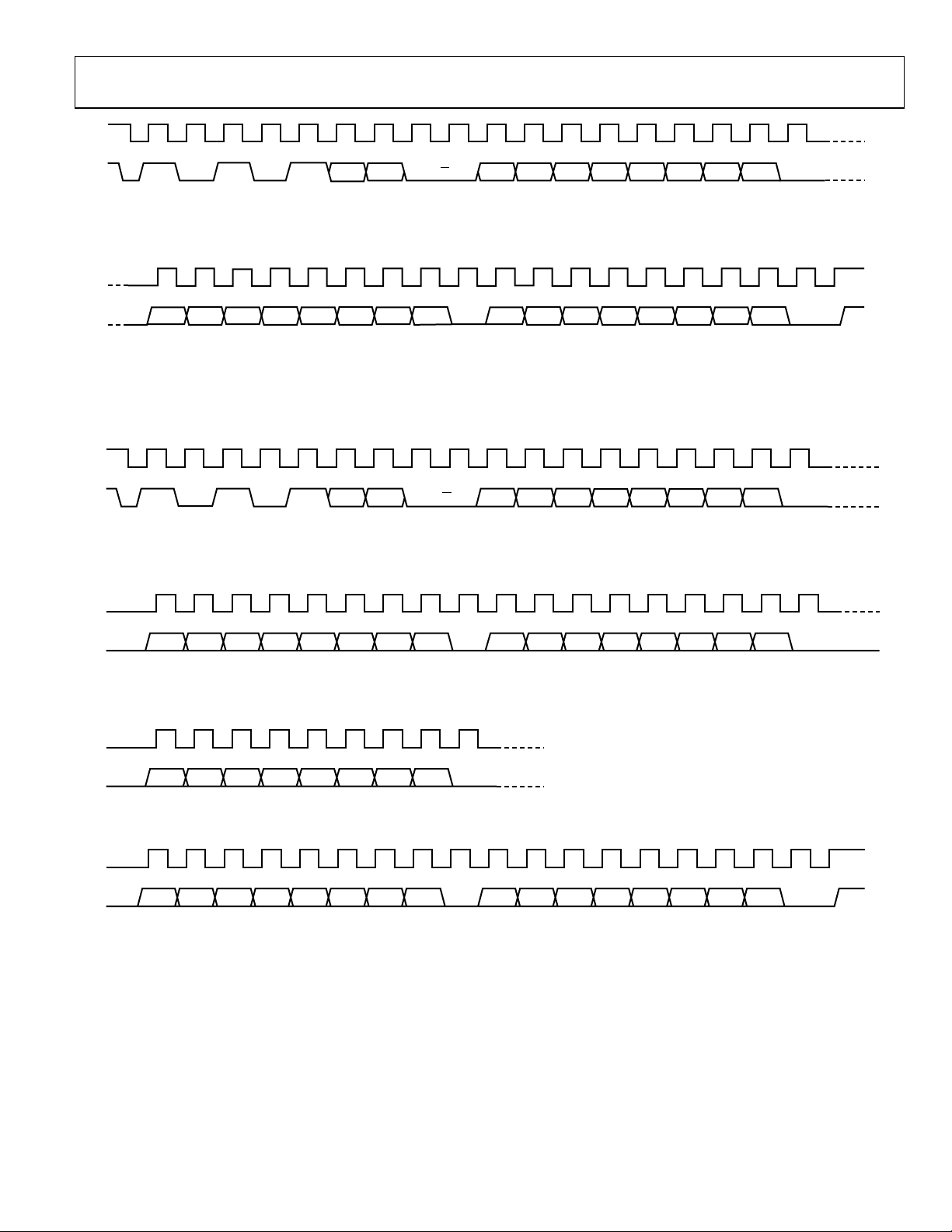
AD5381
A
A
SDA
SDA
SDA
SDA
SCL
SD
START COND
BY MASTER
SCL
SD
SCL
START COND
BY MASTER
SCL
1 0 1 0 1 AD1 AD0 R/W 0 0 A5 A4 A3 A2 A1 A0
ACK BY
ADDRESS BYTE
REG1 REG0 MSB LSB MSB LSB
MOST SIGNIFICANT BYTE LEAST SIGNIFICANT BYTE
AD538x
Figure 31. 4-Byte AD5381, I
1
0 1 0 0 0 A5 A4 A3 A2 A1 A01 AD1 AD0 R/W
ACK BY
ADDRESS BYTE POINTER BYTE FOR CHANNEL "N"
AD538x
MSB ACK BY
POINTER BYTE
ACK BY
AD538x
2
C Write Operation
MSB
AD538x
ACK BY
AD538x
ACK BY
AD538x
STOP
COND
BY
MASTER
03732-031
REG1 REG0 MSB LSB MSB LSB
SCL
SCL
ACK BY
MOST SIGNIFICANT DATA BYTE
0 0 A5 A4 A3 A2 A1 A0
MSB ACK BY
POINTER BYTE FOR CHANNEL "NEXT CHANNEL"
REG1 REG0 MSB LSB MSB LSB
MOST SIGNIFICANT DATA BYTE LEAST SIGNIFICANT DATA BYTE
DATA FOR CHANNEL "NEXT CHANNEL"
Figure 32. 3-Byte AD5381, I
AD538x
DATA FOR CHANNEL "N"
AD538x
ACK BY
AD538x
2
LEAST SIGNIFICANT DATA BYTE
C Write Operation
ACK BY
AD538x
ACK BY
AD538x
STOP COND
BY MASTER
03732-032
Rev. B | Page 29 of 40

AD5381
2-Byte Mode
Following initialization of 2-byte mode, the user can update
channels sequentially. The device address byte is only required
once and the pointer address pointer is configured for autoincrement or burst mode.
The user must begin with an address byte (R/
which the DAC acknowledges that it is prepared to receive
data by pulling SDA low. The address byte is followed by a
specific pointer byte (0xFF) that initiates the burst mode of
operation. The address pointer initializes to Channel 0, the data
following the pointer is loaded to Channel 0, and the address
pointer automatically increments to the next address.
The REG0 and REG1 bits in the data byte determine which
register will be updated. In this mode, following the initialization, only the two data bytes are required to update a channel.
The channel address automatically increments from Address 0
to Channel 39 and then returns to the normal 3-byte mode of
operation. This mode allows transmission of data to all
channels in one block and reduces the software overhead in
configuring all channels. A STOP condition at any time exits
this mode. Toggle mode is not supported in 2-byte mode.
Figure 33 shows a typical configuration.
= 0), after
W
PARALLEL INTERFACE
The SER/
interface and disable the serial interfaces.
timing diagram for a parallel write. The parallel interface is
controlled by the following pins.
Pin
CS
Active low device select pin.
Pin
WR
On the rising edge of WR, with CS low, the addresses on Pin A5
to Pin A0 are latched; data present on the data bus is loaded into
the selected input registers.
REG0, REG1 Pins
The REG0 and REG1 pins determine the destination register of
the data being written to the AD5381. See
Pin A5 to Pin A0
Each of the 40 DAC channels can be individually addressed.
Pin DB11 to Pin DB0
The AD5381 accepts a straight 12-bit parallel word on DB11 to
DB0, where DB11 is the MSB and DB0 is the LSB.
pin must be tied low to enable the parallel
PA R
Figure 7 shows the
Table 11.
SCL
SDA
START COND
BY MASTER
SCL
SDA
SCL
SDA
SCL
SDA
1 0 1 0 1 AD1 AD0 R/W A7 = 1 A6 = 1 A5 = 1 A4 = 1 A3 = 1 A2 = 1 A1 = 1 A0 = 1
ACK BY
ADDRESS BYTE POINTER BYTE
REG1 REG0 MSB LSB MSB LSB
MOST SIGNIFICANT DATA BYTE
REG1 REG0 MSB LSB MSB LSB
MOST SIGNIFICANT DATA BYTE
REG1 REG0 MSB LSB MSB LSB
MOST SIGNIFICANT DATA BYTE
CONVERTER
CONVERTER
CHANNEL N DATA FOLLOWED BY STOP
Figure 33. 2-Byte, 1
MSB ACK BY
ACK BY
AD538x
CHANNEL 0 DATA
ACK BY
CHANNEL 1 DATA
ACK BY
CONVERTER
2
C Write Operation
LEAST SIGNIFICANT DATA BYTE
LEAST SIGNIFICANT DATA BYTE
LEAST SIGNIFICANT DATA BYTE
CONVERTER
CONVERTER
ACK BY
AD538x
ACK BY
ACK BY
CONVERTER
STOP
COND
BY
MASTER
03732-033
Rev. B | Page 30 of 40

AD5381
MICROPROCESSOR INTERFACING
Parallel Interface
The AD5381 can be interfaced to a variety of 16-bit microcontrollers or DSP processors.
Figure 35 shows the AD5381 family
interfaced to a generic 16-bit microcontroller/DSP processor.
The lower address lines from the processor are connected to A0
to A5 on the AD5381. The upper address lines are decoded to
provide a
CS, LDAC
signal for the AD5381. The fast interface
timing of the AD5381 allows direct interface to a wide variety
of microcontrollers and DSPs, as shown in
Figure 35.
AD5381 to MC68HC11
The serial peripheral interface (SPI) on the MC68HC11 is
configured for master mode (MSTR = 1), clock polarity bit
(CPOL) = 0, and the clock phase bit (CPHA) = 1. The SPI is
configured by writing to the SPI control register (SPCR)—see
the MC68HC11 user manual. SCK of the MC68HC11 drives the
SCLK of the AD5381, the MOSI output drives the serial data
line (D
D
) of the AD5381, and the MISO input is driven from
IN
. The SYNC signal is derived from a port line (PC7).
OUT
μ
CONTROLLER/
DSP PROCESSOR
1
When data is being transmitted to the AD5381, the
SYNC
line
is taken low (PC7). Data appearing on the MOSI output is valid
on the falling edge of SCK. Serial data from the MC68HC11 is
transmitted in 8-bit bytes with only eight falling clock edges
occurring in the transmit cycle.
MC68HC11
MISO
MOSI
SCK
PC7
Figure 34. AD5381-to-MC68HC11 Interface
AD5381
DVDD
AD5381
SER/PAR
RESET
SDO
DIN
SCLK
SYNC
2
SPI/I
C
03731-034
D15
DATA
BUS
D0
UPPER BITS OF
ADDRESS BUS
A5
A4
A3
A2
A1
A0
R/W
1
ADDITIONAL PINS OMITTED FOR CLARITY.
Figure 35. AD5381-to-Parallel Interface
ADDRESS
DECODE
REG1
REG0
D11
D0
CS
LDAC
A5
A4
A3
A2
A1
A0
WR
03732-035
Rev. B | Page 31 of 40

AD5381
AD5381 to PIC16C6x/7x
The PIC16C6x/7x synchronous serial port (SSP) is configured
as an SPI master with the Clock Polarity Bit = 0. This is done
by writing to the synchronous serial port control register
(SSPCON). See the PIC16/17 microcontroller user manual.
In this example I/O, Port RA1 is being used to pulse
SYNC
and enable the serial port of the AD5381. This microcontroller
transfers only eight bits of data during each serial transfer
operation; therefore, three consecutive read/write operations
may be needed depending on the mode.
Figure 36 shows the
connection diagram.
PIC16C6X/7X
SDI/RC4
SDO/RC5
SCK/RC3
RA1
Figure 36. AD5381-to-PIC16C6x/7x Interface
DVDD
AD5381
SER/PAR
RESET
SDO
DIN
SCLK
SYNC
2
SPI/I
C
AD5381 to 8051
The AD5381 requires a clock synchronized to the serial data.
The 8051 serial interface must therefore be operated in Mode 0.
In this mode, serial data enters and exits through RxD, and a
shift clock is output on TxD.
Figure 37 shows how the 8051 is
connected to the AD5381. Because the AD5381 shifts data out
on the rising edge of the shift clock and latches data in on the
falling edge, the shift clock must be inverted. The AD5381
requires its data to be MSB first. Since the 8051 outputs the
LSB first, the transmit routine must take this into account.
03732-036
8XC51
RxD
TxD
P1.1
DVDD
AD5381
SER/PAR
RESET
SDO
DIN
SCLK
SYNC
2
C
SPI/I
Figure 37. AD5381-to-8051 Interface
AD5381 to ADSP-2101/ADSP-2103
Figure 38 shows a serial interface between the AD5381 and the
ADSP-2101/ADSP-2103. The ADSP-2101/ADSP-2103 should
be set up to operate in SPORT transmit alternate framing mode.
The ADSP-2101/ADSP-2103 SPORT is programmed through
the SPORT control register and configured as follows: internal
clock operation, active low framing, and 16-bit word length.
Transmission is initiated by writing a word to the Tx register
after the SPORT has been enabled.
ADSP-2101/
ADSP-2103
DR
DT
SCK
TFS
RFS
Figure 38. AD5381-to-ADSP-2101/ADSP-2103 Interface
DVDD
AD5381
SER/PAR
RESET
SDO
DIN
SCLK
SYNC
SPI/I2C
03732-037
03732-038
Rev. B | Page 32 of 40

AD5381
APPLICATION INFORMATION
POWER SUPPLY DECOUPLING
In any circuit where accuracy is important, careful consideration of the power supply and ground return layout helps to
ensure the rated performance. The printed circuit board on
which the AD5381 is mounted should be designed so that the
analog and digital sections are separated and confined to
certain areas of the board. If the AD5381 is in a system where
multiple devices require an AGND-to-DGND connection, the
connection should be made at one point only, a star ground
point established as close to the device as possible.
For supplies with multiple pins (AVDD, DVDD), these pins
should be tied together. The AD5381 should have ample supply
bypassing of 10 μF in parallel with 0.1 μF on each supply,
located as close to the package as possible and ideally right
up against the device. The 10 μF capacitors are the tantalum
bead type. The 0.1 μF capacitor should have low effective series
resistance (ESR) and effective series inductance (ESI), like the
common ceramic types that provide a low impedance path to
ground at high frequencies, to handle transient currents due to
internal logic switching.
The power supply lines of the AD5381 should use as large a
trace as possible to provide low impedance paths and reduce
the effects of glitches on the power supply line. Fast switching
signals such as clocks should be shielded with digital ground
to avoid radiating noise to other parts of the board, and should
never be run near the reference inputs. A ground line routed
between the D
between them (this is not required on a multilayer board
because there will be a separate ground plane, but separating the lines will help). It is essential to minimize noise on
the REFOUT/REFIN line.
and SCLK lines will help reduce crosstalk
IN
externally from either an ADR421 or ADR431 2.5 V reference.
Suitable external references for the AD5381-3 include the
ADR280 1.2 V reference. The reference should be decoupled at
the REFOUT/REFIN pin of the device with a 0.1 μF capacitor.
AVDD DVDD
0.1μF
ADR431/
ADR421
REFOUT/REFIN
0.1μF
REFGND
Figure 39. Typical Configuration with External Reference
10μF 0.1μF
AVDD DVDD
AD5381-5
VOUT39
SIGNAL_GNDDAC_GND
AGND
VOUT0
DGND
Figure 40 shows a typical configuration when using the internal
reference. On power-up, the AD5381 defaults to an external
reference; therefore, the internal reference needs to be configured and turned on via a write to the AD5381 control register.
Control Register Bit CR10 allows the user to choose the
reference value; Bit CR8 is used to select the internal reference.
It is recommended to use the 2.5 V reference when AVDD =
5 V, and the 1.25 V reference when AVDD= 3 V.
AVDD DVDD
0.1μF
10μF 0.1μF
03732-039
Avoid crossover of digital and analog signals. Traces on
opposite sides of the board should run at right angles to
each other. This reduces the effects of feedthrough through
the board. A micro-strip technique is by far the best, but is
not always possible with a double-sided board. In this technique, the component side of the board is dedicated to the
ground plane while signal traces are placed on the solder side.
TYPICAL CONFIGURATION CIRCUIT
Figure 39 shows a typical configuration for the AD5381-5
when configured for use with an external reference. In the
circuit shown, all AGND, SIGNAL_GND, and DAC_GND pins
are tied together to a common AGND. AGND and DGND are
connected together at the AD5381 device. On power-up, the
AD5381 defaults to external reference operation. All AVDD
lines are connected together and driven from the same 5 V
source. It is recommended to decouple close to the device
with a 0.1 μF ceramic and a 10 μF tantalum capacitor. In this
application, the reference for the AD5381-5 is provided
Rev. B | Page 33 of 40
AVDD DVDD
REFOUT/REFIN
0.1μF
REFGND
Figure 40. Typical Configuration with Internal Reference
AD5381
SIGNAL_GNDDAC_GND
AGND
VOUT0
VOUT39
DGND
03732-040
Digital connections have been omitted for clarity. The AD5381
contains an internal power-on reset circuit with a 10 ms brownout time. If the power supply ramp rate exceeds 10 ms, the user
should reset the AD5381 as part of the initialization process to
ensure the calibration data is loaded correctly into the device.

AD5381
MONITOR FUNCTION
The AD5381 channel monitor function consists of a multiplexer
addressed via the interface, allowing any channel output to be
routed to this pin for monitoring using an external ADC. In
channel monitor mode, VOUT39 becomes the MON_OUT pin,
to which all monitored signals are routed. The channel monitor
function must be enabled in the control register before any
channels are routed to MON_OUT.
decoding information required to route any channel to
MON_OUT. Selecting Channel Address 63 three-states
MON_OUT.
Figure 41 shows a typical monitoring circuit
implemented using a 12-bit SAR ADC in a 6-lead SOT-23
package. The controller output port selects the channel to be
monitored, and the input port reads the converted data from
the ADC.
VOUT0
VOUT38
DAC_GND SIGNAL_GND
AVDD
AD5381
Figure 41. Typical Channel Monitoring Circuit
DIN
SYNC
SCLK
AGND
TOGGLE MODE FUNCTION
The toggle mode function allows an output signal to be generated using the
DAC data registers. This function is configured using the SFR
control register as follows. A write with REG1 = REG0 = 0 and
A5 to A0 = 001100 specifies a control register write. The toggle
mode function is enabled in groups of eight channels using Bit
CR4 to Bit CR0 in the control register. See the AD5381 control
register description.
mode implementation. Each of the 40 DAC channels on the
AD5381 contain an A and B data register.
control signal that switches between two
LDAC
Figure 42 shows a block diagram of toggle
Table 1 8 contains the
VDD
AD7476
VINVOUT39/MON_OUT
CS
SCLK
SDATA
GND
OUTPUT PORT
INPUT PORT
CONTROLLER
03732-041
Note that B registers can only be loaded when toggle mode is
enabled. The sequence of events when configuring the AD5381
for toggle mode is
1. Enable toggle mode for the required channels via the
control register.
2. Load data to the A registers.
3. Load data to the B registers.
4. Apply
is used to switch between the A and B registers in
LDAC
determining the analog output. The first
LDAC
.
configures the
LDAC
output to reflect data in the A registers. This mode offers significant advantages if the user wants to generate a square wave at
the output of all 40 channels, as might be required to drive a
liquid crystal-based variable optical attenuator.
In this case, the user writes to the control register and enables
the toggle function by setting CR4 to CR2 = 0, thus enabling the
five groups of eight for toggle mode operation. The user must
then load data to all 40 A and B registers. Toggling
LDAC
sets
the output values to reflect the data in the A and B registers.
The frequency of the
determines the frequency of the
LDAC
square wave output.
Toggle mode is disabled via the control register. The first
LDAC
following the disabling of the toggle mode will update the outputs with the data contained in the A registers.
THERMAL MONITOR FUNCTION
The AD5381 contains a temperature shutdown function to
protect the chip if multiple outputs are shorted. The shortcircuit current of each output amplifier is typically 40 mA.
Operating the AD5381 at 5 V leads to a power dissipation of
200 mW per shorted amplifier. With five channels shorted, this
leads to an extra watt of power dissipation. For the 100-lead
LQFP, the θ
The thermal monitor is enabled by the user via CR6 in the
control register. The output amplifiers on the AD5381 are
automatically powered down if the die temperature exceeds
approximately 130°C. After a thermal shutdown has occurred,
the user can re-enable the part by executing a soft power-up if
the temperature has dropped below 130°C or by turning off the
thermal monitor function via the control register.
is typically 44°C/W.
JA
Rev. B | Page 34 of 40

AD5381
DATA
REGISTER
A
INPUT
INPUT
DATA
REGISTER
A/B
DATA
REGISTER
B
Figure 42. Toggle Mode Function
OPTICAL ATTENUATORS
Based on its high channel count, high resolution, monotonic
behavior, and high level of integration, the AD5381 is ideally
targeted at optical attenuation applications used in dynamic
gain equalizers, variable optical attenuators (VOAs), and optical
add-drop multiplexers (OADMs). In these applications, each
wavelength is individually extracted using an arrayed wave
guide; its power is monitored using a photodiode, transimpedance amplifier and ADC in a closed-loop control system. The
AD5381 controls the optical attenuator for each wavelength,
ensuring that the power is equalized in all wavelengths before
being multiplexed onto the fiber. This prevents information loss
and saturation from occurring at amplification stages further
along the fiber.
DAC
REGISTER
12-BIT DAC
VOUT
LDAC
CONTROL INPUT
03732-042
UTILIZING FIFO
The AD5381 FIFO mode optimizes total system update rates
in applications where a large number of channels need to be
updated. FIFO mode is only available when parallel interface
mode is selected. The FIFO EN pin is used to enable the FIFO.
The status of FIFO EN is sampled during the initialization
sequence. Therefore, the FIFO status can only be changed by
resetting the device.
In a telescope that provides for the cancel-lation of atmospheric
distortion, for example, a large number of channels need to be
updated in a short period of time. In such systems, as many as
400 channels need to be updated within 40 μs. Four-hundred
channels require the use of 10 AD5381s. With FIFO mode
enabled, the data write cycle time is 40 ns; therefore, each group
consisting of 40 channels can be fully loaded in 1.6 μs. In FIFO
mode, a complete group of 40 chan-nels will update in 14.4 μs.
The time taken to update all 400 channels is
14.4 μs + 9 × 1.6 μs = 28.8 μs.
Figure 44 shows the FIFO operation scheme.
DWDM
IN
ADD
PORTS
11
12
AWG
1n–1
1n
Figure 43. OADM Using the AD5381 as Part of an Optical Attenuator
OPTICAL
SWITCH
DROP
PORTS
ATTENUATOR
ATTENUATOR
ATTENUATOR
ATTENUATOR
AD5381,
40-CHANNEL,
12-BIT DAC
PHOTODIODES
TIA/LOG AMP
(AD8304/AD8305)
N:1 MULTIPLEXER
16-BIT ADCCONTROLLER
DWDM
AWG
ADG731
(40:1 MUX)
AD7671
(0V TO 5V, 1MSPS)
OUT
FIBREFIBRE
03732-043
Rev. B | Page 35 of 40

AD5381
GROUP A
CHNLS 0–39
FIFO DATA LOAD
GROUP A
1.6μs
GROUP B
CHNLS 40–79
1.6μs
GROUP C
CHNLS
80–119
FIFO DATA LOAD
GROUP B
GROUP D
CHNLS
120–159
GROUP E
CHNLS
160–199
GROUP F
CHNLS
200–239
GROUP G
CHNLS
240–279
GROUP H
CHNLS
280–319
FIFO DATA LOAD
GROUP I
CHNLS
320–359
GROUP J
GROUP J
CHNLS
360–399
1.6μs
14.4μs
OUTPUT UPDATE
TIME FOR GROUP A
14.4μs
Figure 44. Using FIFO Mode 400 Channels Updated in Under 30 μs
OUTPUT UPDATE
TIME FOR GROUP B
TIME TO UPDATE 400 CHANNELS = 28.8μs
OUTPUT UPDATE
TIME FOR GROUP J
14.4μs
03732-044
Rev. B | Page 36 of 40

AD5381
OUTLINE DIMENSIONS
16.00 BSC SQ
1.60 MAX
0.75
0.60
0.45
1
14.00 BSC SQ
PIN 1
76100
75
12.00
REF
51
50
1.45
1.40
1.35
0.15
SEATING
0.05
PLANE
VIEW A
ROTATED 90° CCW
0.20
0.09
7°
3.5°
0°
0.08 MAX
COPLANARITY
COMPLIANT TO JEDEC STANDARDS MS-026BED
25
VIEW A
26
LEAD PITCH
TOP VIEW
(PINS DOWN)
0.50
BSC
0.27
0.22
0.17
Figure 45. 100-Lead Low Profile Quad Flat Package [LQFP]
(ST-100)
Dimensions shown in millimeters
ORDERING GUIDE
Temperature
Model Resolution
Range
AVDD Range
AD5381BST-3 12 Bits –40°C to +85°C 2.7 V to 3.6 V 40 ±1 100-Lead LQFP ST-100
AD5381BST-3-REEL 12 Bits –40°C to +85°C 2.7 V to 3.6 V 40 ±1 100-Lead LQFP ST-100
AD5381BSTZ-3
1
12 Bits –40°C to +85°C 2.7 V to 3.6 V 40 ±1 100-Lead LQFP ST-100
AD5381BSTZ-3-REEL112 Bits –40°C to +85°C 2.7 V to 3.6 V 40 ±1 100-Lead LQFP ST-100
AD5381BST-5 12 Bits –40°C to +85°C 4.5 V to 5.5 V 40 ±1 100-Lead LQFP ST-100
AD5381BST-5-REEL 12 Bits –40°C to +85°C 4.5 V to 5.5 V 40 ±1 100-Lead LQFP ST-100
AD5381BSTZ-5
1
12 Bits –40°C to +85°C 4.5 V to 5.5 V 40 ±1 100-Lead LQFP ST-100
AD5381BSTZ-5-REEL112 Bits –40°C to +85°C 4.5 V to 5.5 V 40 ±1 100-Lead LQFP ST-100
EVAL-AD5381EB Evaluation Kit
1
Z = Pb-free part.
2
I
C Standard Specification as defined by Philips.
Output
Channels
Linearity
Error (LSB)
Package
Description
Package
Option
Rev. B | Page 37 of 40

AD5381
NOTES
Rev. B | Page 38 of 40

AD5381
NOTES
Rev. B | Page 39 of 40

AD5381
NOTES
Purchase of licensed I2C components of Analog Devices or one of its sublicensed Associated Companies conveys a license for the purchaser under the Philips I2C Patent
Rights to use these components in an I2C system, provided that the system conforms to the I2C Standard Specification as defined by Philips.
© 2005 Analog Devices, Inc. All rights reserved. Trademarks and
registered trademarks are the property of their respective owners.
D03732–0–8/05(B)
Rev. B | Page 40 of 40
 Loading...