Analog Devices AD5380 Datasheet
40-Channel, 3 V/5 V, Single-Supply,
FEATURES
Guaranteed monotonic
INL error: ±4 LSB max
On-chip 1.25 V/2.5 V, 10 ppm/°C reference
Temperature range: –40°C to +85°C
Rail-to-rail output amplifier
Power down
Package type: 100-lead LQFP (14 mm × 14 mm)
User Interfaces:
Parallel
Serial (SPI®/QSPI™/MICROWIRE™/DSP compatible,
featuring data readback)
I2C® compatible
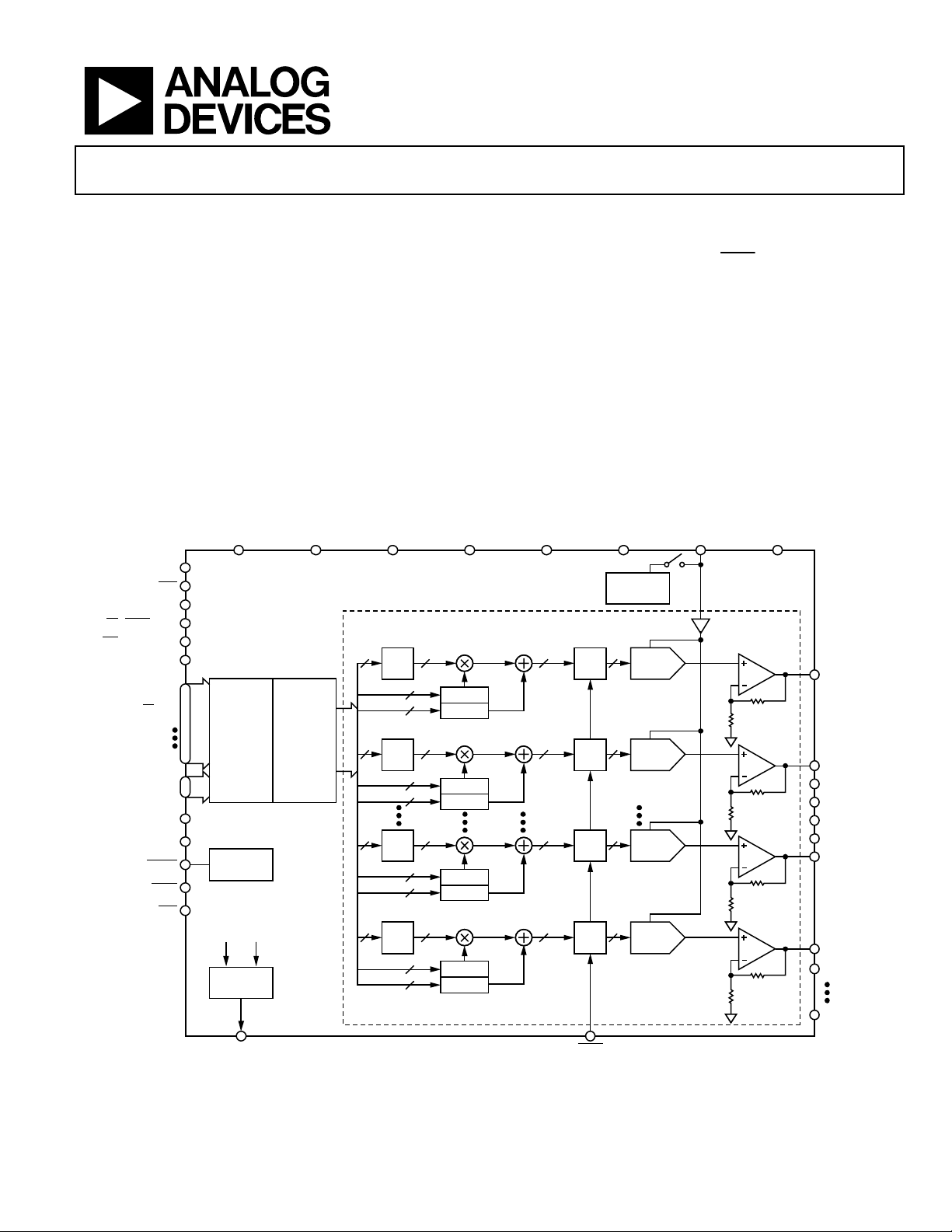
DVDD (×3) DGND (×3) AVDD (×5) AGND (×5) DAC GND (×5) REFGND REFOUT/REFIN SIGNAL GND (×5)
SER/PAR
FIFO EN
CS/(SYNC/AD 0)
WR/(DCEN/AD 1)
SDO
DB13/(DIN/SDA)
DB12/(SCLK/SCL)
DB11/(SPI/I2C)
DB10
DB0
REG 0
REG 1
RESET
BUSY
CLR
PD
A5
A0
INTERFACE
CONTROL
POWER-ON
V
0………V
OUT
AD5380
LOGIC
RESET
39-TO-1
MUX
OUT
FIFO
+
STATE
MACHINE
+
CONTROL
LOGIC
38
14-Bit, Voltage Output DAC
INTEGRATED FUNCTIONS
Channel monitor
Simultaneous output update via
Clear function to user programmable code
Amplifier boost mode to optimize slew rate
User programmable offset and gain adjust
Toggle mode enables square wave generation
Thermal monitor
APPLICATIONS
Variable optical attenuators (VOA)
Level setting (ATE)
Optical micro-electro-mechanical systems (MEMS)
Control systems
Instrumentation
FUNCTIONAL BLOCK DIAGRAM
INPUT
REG 0
14
14
INPUT
REG 1
14
14
INPUT
REG 6
14
14
INPUT
REG 7
14
14
m REG 0
c REG 0
m REG 1
c REG 1
m REG 6
c REG 6
m REG 7
c REG 7
×5
DAC
REG 0
DAC
REG 1
DAC
REG 6
DAC
REG 7
1.25V/2.5V
REFERENCE
1414 1414
DAC 0
1414 1414
DAC 1
1414 1414
DAC 6
1414 1414
DAC 7
LDAC
R
R
R
R
R
R
R
R
AD5380
VOUT
VOUT1
VOUT2
VOUT3
VOUT4
VOUT5
VOUT6
VOUT7
VOUT8
VOUT38
VOUT 39/MON_OUT LDAC
Rev. 0
Information furnished by Analog Devices is believed to be accurate and reliable.
However, no responsibility is assumed by Analog Devices for its use, nor for any
infringements of patents or other rights of third parties that may result from its use.
Specifications subject to change without notice. No license is granted by implication
or otherwise under any patent or patent rights of Analog Devices. Trademarks and
registered trademarks are the property of their respective owners.
Figure 1.
One Technology Way, P.O. Box 9106, Norwood, MA 02062-9106, U.S.A.
Tel: 781.329.4700 www.analog.com
Fax: 781.326.8703 © 2004 Analog Devices, Inc. All rights reserved.
03731-0-001

AD5380
TABLE OF CONTENTS
General Description......................................................................... 3
BUSY
and
Functions...................................................... 25
LDAC
Specifications..................................................................................... 4
AD5380-5 Specifications............................................................. 4
AD5380-3 Specifications............................................................. 6
AC Characteristics........................................................................ 7
Timing Characteristics..................................................................... 8
Serial Interface ..............................................................................8
I2C Serial Interface...................................................................... 10
Parallel Interface .........................................................................11
Absolute Maximum Ratings.......................................................... 13
Pin Configurations and Function Descriptions......................... 14
Terminology ....................................................................................17
Typical Performance Characteristics ...........................................18
Functional Description.................................................................. 21
DAC Architecture—General..................................................... 21
Data Decoding............................................................................ 21
FIFO Operation in Parallel Mode............................................ 25
Power-On Reset.......................................................................... 25
Power-Down ............................................................................... 25
AD5380 Interfaces.......................................................................... 26
DSP, SPI, Microwire Compatible Serial Interfaces................. 26
I2C Serial Interface ..................................................................... 28
Parallel Interface......................................................................... 30
Microprocessor Interfacing....................................................... 31
Application Information................................................................ 33
Power Supply Decoupling......................................................... 33
Typical Configuration Circuit .................................................. 33
AD5380 Monitor Function .......................................................34
Toggle Mode Function............................................................... 34
Thermal Monitor Function....................................................... 35
AD5380 in a MEMS Based Optical Switch............................. 35
On-Chip Special Function Registers (SFR) ............................22
SFR Commands.......................................................................... 22
Hardware Functions....................................................................... 25
Reset Function ............................................................................25
Asynchronous Clear Function.................................................. 25
REVISION HISTORY
5/04—Revision 0: Initial Version
Optical Attenuators .................................................................... 36
Utilizing the AD5380 FIFO....................................................... 37
Outline Dimensions....................................................................... 38
Ordering Guide .......................................................................... 38
Rev. 0 | Page 2 of 40
AD5380
GENERAL DESCRIPTION
The AD5380 is a complete, single-supply, 40-channel, 14-bit
DAC available in a 100-lead LQFP package. All 40 channels
have an on-chip output amplifier with rail-to-rail operation.
The AD5380 includes a programmable internal 1.25 V/2.5 V,
10 ppm/°C reference, an on-chip channel monitor function that
multiplexes the analog outputs to a common MON_OUT pin
for external monitoring, and an output amplifier boost mode
that allows optimization of the amplifier slew rate. The AD5380
contains a double-buffered parallel interface that features a
20 ns
pulse width, an SPI/QSPI/MICROWIRE/DSP
WR
compatible serial interface with interface speeds in excess of
2
30 MHz, and an I
C compatible interface that supports a
400 kHz data transfer rate.
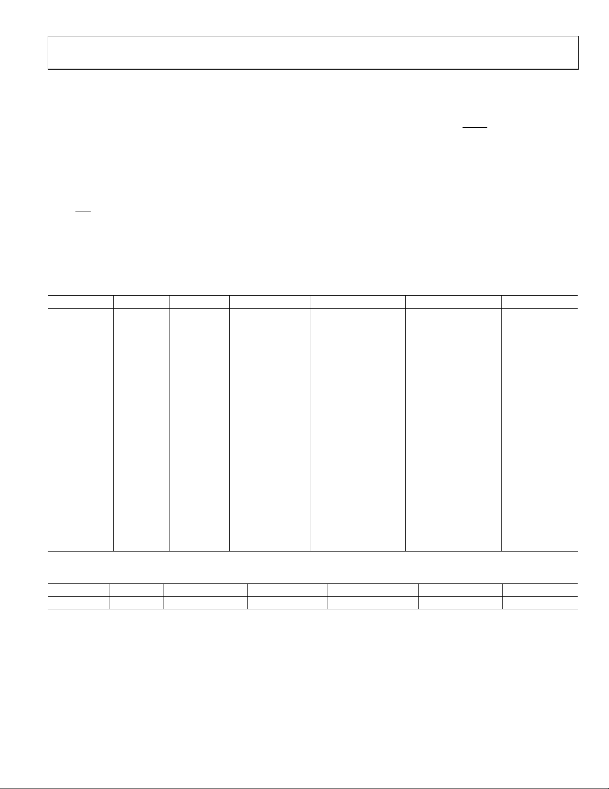
Table 1. Other High Channel Count, Low Voltage, Single Supply DACs in Portfolio
Model Resolution AVDD Range Output Channels Linearity Error (LSB) Package Description Package Option
AD5381BST-5 12 Bits 4.5 V to 5.5 V 40 ±1 100-Lead LQFP ST-100
AD5381BST-3 12 Bits 2.7 V to 3.6 V 40 ±1 100-Lead LQFP ST-100
AD5384BBC-5 14 Bits 4.5 V to 5.5 V 40 ±4 100-Lead CSPBGA BC-100
AD5384BBC-3 14 Bits 2.7 V to 3.6 V 40 ±4 100-Lead CSPBGA BC-100
AD5382BST-5 14 Bits 4.5 V to 5.5 V 32 ±4 100-Lead LQFP ST-100
AD5382BST-3 14 Bits 2.7 V to 3.6 V 32 ±4 100-Lead LQFP ST-100
AD5383BST-5 12 Bits 4.5 V to 5.5 V 32 ±1 100-Lead LQFP ST-100
AD5383BST-3 12 Bits 2.7 V to 3.6 V 32 ±1 100-Lead LQFP ST-100
AD5390BST-5 14 Bits 4.5 V to 5.5 V 16 ±3 52-Lead LQFP ST-52
AD5390BCP-5 14 Bits 4.5 V to 5.5 V 16 ±3 64-Lead LFCSP CP-64
AD5390BST-3 14 Bits 2.7 V to 3.6 V 16 ±3 52-Lead LQFP ST-52
AD5390BCP-3 14 Bits 2.7 V to 3.6 V 16 ±3 64-Lead LFCSP CP-64
AD5391BST-5 12 Bits 4.5 V to 5.5 V 16 ±1 52-Lead LQFP ST-52
AD5391BCP-5 12 Bits 4.5 V to 5.5 V 16 ±1 64-Lead LFCSP CP-64
AD5391BST-3 12 Bits 2.7 V to 3.6 V 16 ±1 52-Lead LQFP ST-52
AD5391BCP-3 12 Bits 2.7 V to 3.6 V 16 ±1 64-Lead LFCSP CP-64
AD5392BST-5 14 Bits 4.5 V to 5.5 V 8 ±3 52-Lead LQFP ST-52
AD5392BCP-5 14 Bits 4.5 V to 5.5 V 8 ±3 64-Lead LFCSP CP-64
AD5392BST-3 14 Bits 2.7 V to 3.6 V 8 ±3 52-Lead LQFP ST-52
AD5392BCP-3 14 Bits 2.7 V to 3.6 V 8 ±3 64-Lead LFCSP CP-64
Table 2. 40-Channel, Bipolar Voltage Output DAC
Model Resolution Analog Supplies Output Channels Linearity Error (LSB) Package Package Option
AD5379ABC 14 Bits ±11.4 V to ±16.5 V 40 ±3 108-Lead CSPBGA BC-108
An input register followed by a DAC register provides double
buffering, allowing the DAC outputs to be updated independently or simultaneously using the
LDAC
input.
Each channel has a programmable gain and offset adjust
register that allows the user to fully calibrate any DAC channel. Power consumption is typically 0.25 mA/channel with
boost off.
Rev. 0 | Page 3 of 40

AD5380
SPECIFICATIONS
AD5380-5 SPECIFICATIONS
Table 3 . AVDD = 4.5 V to 5.5 V; DVDD = 2.7 V to 5.5 V, AGND = DGND = 0 V; External REFIN = 2.5 V;
all specifications T
MIN
to T
Parameter AD5380-51 Unit Test Conditions/Comments
ACCURACY
Resolution 14 Bits
Relative Accuracy2 (INL) ±4 LSB max ±1 LSB typical
Differential Nonlinearity (DNL) –1/+2 LSB max Guaranteed monotonic by design over temperature
Zero-Scale Error 4 mV max
Offset Error ±4 mV max Measured at code 32 in the linear region
Offset Error TC ±5 µV/°C typ
Gain Error ±0.024 % FSR max At 25°C
±0.06 % FSR max T
Gain Temperature Coefficient3 2 ppm FSR/°C typ
DC Crosstalk3 0.5 LSB max
REFERENCE INPUT/OUTPUT
Reference Input3
Reference Input Voltage 2.5 V ±1% for specified performance, AVDD = 2 × REFIN + 50 mV
DC Input Impedance 1 MΩ min Typically 100 MΩ
Input Current ±1 µA max Typically ±30 nA
Reference Range 1 to VDD/2 V min/max
Reference Output4
Output Voltage 2.495/2.505 V min/max At ambient. CR12 = 1. Optimized for 2.5 V operation.
1.22/1.28 V min/max CR12 = 0
Reference TC ±10 ppm/°C max Temperature range: +25°C to +85°C
±15 ppm/°C max Temperature range: −40°C to +85°C
Output Impedance 2.2 kΩ typ
OUTPUT CHARACTERISTICS3
Output Voltage Range2 0/AVDD V min/max
Short-Circuit Current 40 mA max
Load Current ±1 mA max
Capacitive Load Stability
RL = ∞ 200 pF max
RL = 5 kΩ 1000 pF max
DC Output Impedance 0.5 Ω max
MONITOR PIN
Output Impedance 500 Ω typ
Three-State Leakage Current 100 nA typ
LOGIC INPUTS (EXCEPT SDA/SCL)3 DVDD = 2.7 V to 5.5 V
VIH, Input High Voltage 2 V min
VIL, Input Low Voltage 0.8 V max
Input Current ±10 µA max Total for all pins. TA = T
Pin Capacitance 10 pF max
LOGIC INPUTS (SDA, SCL ONLY)
VIH, Input High Voltage 0.7 DVDD V min SMBus compatible at DVDD< 3.6 V
VIL, Input Low Voltage 0.3 DVDD V max SMBus compatible at DVDD< 3.6 V
IIN, Input Leakage Current ±1 µA max
V
, Input Hysteresis 0.05 DVDD V min
HYST
CIN, Input Capacitance 8 pF typ
Glitch Rejection 50 ns max Input filtering suppresses noise spikes of less than 50 ns
, unless otherwise noted
MAX
to T
MAX
MIN
Enabled via CR10 in the AD5380 control register.
CR12 selects the reference voltage.
to T
MAX
MIN
Rev. 0 | Page 4 of 40
AD5380
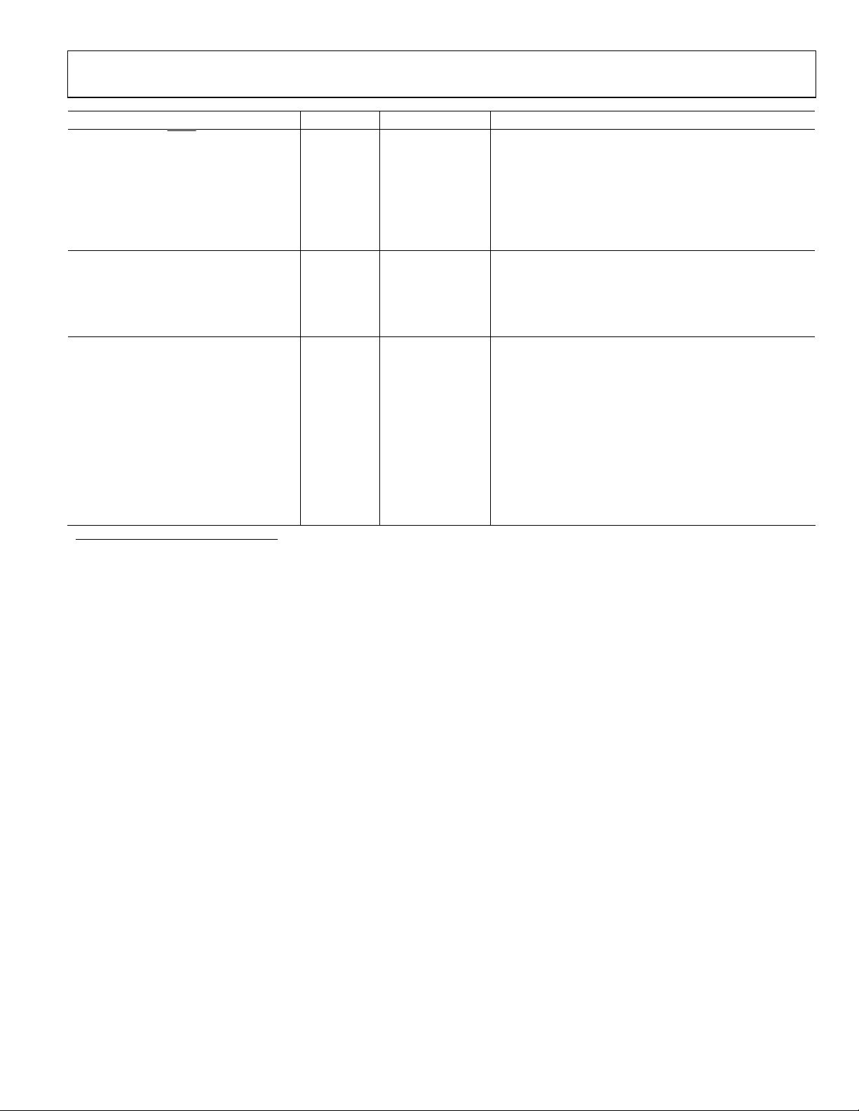
Parameter AD5380-51 Unit Test Conditions/Comments
LOGIC OUTPUTS (BUSY, SDO)3
VOL, Output Low Voltage 0.4 V max DVDD = 5 V ± 10%, sinking 200 µA
VOH, Output High Voltage DVDD – 1 V min DVDD = 5 V ± 10%, sourcing 200 µA
VOL, Output Low Voltage 0.4 V max DVDD = 2.7 V to 3.6 V, sinking 200 µA
VOH, Output High Voltage DVDD – 0.5 V min DVDD = 2.7 V to 3.6 V, sourcing 200 µA
High Impedance Leakage Current ±1 µA max SDO only
High Impedance Output Capacitance 5 pF typ SDO only
LOGIC OUTPUT (SDA)3
VOL, Output Low Voltage 0.4 V max I
0.6 V max I
Three-State Leakage Current ±1 µA max
Three-State Output Capacitance 8 pF typ
POWER REQUIREMENTS
AVDD 4.5/5.5 V min/max
DVDD 2.7/5.5 V min/max
Power Supply Sensitivity3
∆Mid Scale/∆ΑVDD –85 dB typ
AIDD 0.375 mA/channel max Outputs unloaded, Boost off. 0.25 mA/channel typ
0.475 mA/channel max Outputs unloaded, Boost on. 0.325 mA/channel typ
DIDD 1 mA max VIH = DVDD, VIL = DGND
AIDD (Power-Down) 2 µA max Typically 200 nA
DIDD (Power-Down) 20 µA max Typically 3 µA
Power Dissipation 80 mW max Outputs unloaded, Boost off, AVDD = DVDD = 5 V
1
AD5380-5 is calibrated using an external 2.5 V reference. Temperature range for all versions: –40°C to +85°C.
2
Accuracy guaranteed from V
3
Guaranteed by characterization, not production tested.
4
Default on the AD5380-5 is 2.5 V. Programmable to 1.25 V via CR12 in the AD5380 control register; operating the AD5380-5 with a 1.25 V reference will lead to
degraded accuracy specifications.
= 10 mV to AVDD – 50 mV.
OUT
= 3 mA
SINK
= 6 mA
SINK
Rev. 0 | Page 5 of 40

AD5380
AD5380-3 SPECIFICATIONS
Table 4 . AVDD = 2.7 V to 3.6 V; DVDD = 2.7 V to 5.5 V, AGND = DGND = 0 V; external REFIN = 1.25 V;
all specifications T
MIN
to T
Parameter AD5380-31 Unit Test Conditions/Comments
ACCURACY
Resolution 14 Bits
Relative Accuracy2 (INL) ±4 LSB max
Differential Nonlinearity (DNL) –1/+2 LSB max Guaranteed monotonic over temperature
Zero-Scale Error 4 mV max
Offset Error ±4 mV max Measured at Code 64 in the linear region
Offset Error TC ±5 µV/°C typ
Gain Error ±0.024 % FSR max At 25°C
±0.06 % FSR max T
Gain Temperature Coefficient3 2 ppm FSR/°C typ
DC Crosstalk3 0.5 LSB max
REFERENCE INPUT/OUTPUT
Reference Input3
Reference Input Voltage 1.25 V ±1% for specified performance
DC Input Impedance 1 MΩ min Typically 100 MΩ
Input Current ±1 µA max Typically ±30 nA
Reference Range 1 to AVDD/2 V min/max
Reference Output4
Output Voltage 1.247/1.253 V min/max At ambient. CR12 = 0. Optimized for 1.25 V operation.
2.43/2.57 V min/max CR12 = 1.
Reference TC ±10 ppm/°C max Temperature range: +25°C to +85°C
±15 ppm/°C max Temperature range: −40°C to +85°C
Output Impedance 2.2 kΩ typ
OUTPUT CHARACTERISTICS3
Output Voltage Range2 0/AVDD V min/max
Short-Circuit Current 40 mA max
Load Current ±1 mA max
Capacitive Load Stability
RL = ∞ 200 pF max
RL = 5 kΩ 1000 pF max
DC Output Impedance 0.5 Ω max
MONITOR PIN
Output Impedance 500 Ω typ
Three-State Leakage Current 100 nA typ
LOGIC INPUTS (EXCEPT SDA/SCL)3 DVDD = 2.7 V to 3.6 V
VIH, Input High Voltage 2 V min
V
Input Low Voltage 0.8 V max
IL,
Input Current ±10 µA max Total for all pins. TA = T
Pin Capacitance 10 pF max
LOGIC INPUTS (SDA, SCL ONLY)
VIH, Input High Voltage 0.7 DVDD V min SMBus compatible at DVDD < 3.6 V
VIL, Input Low Voltage 0.3 DVDD V max SMBus compatible at DVDD < 3.6 V
IIN, Input Leakage Current ±1 µA max
V
, Input Hysteresis 0.05 DVDD V min
HYST
CIN, Input Capacitance 8 pF typ
Glitch Rejection 50 ns max Input filtering suppresses noise spikes of less than 50 ns
, unless otherwise noted
MAX
to T
MAX
MIN
Enabled via CR10 in the AD5380 control register.
CR12 selects the reference voltage.
to T
MAX
MIN
Rev. 0 | Page 6 of 40
AD5380
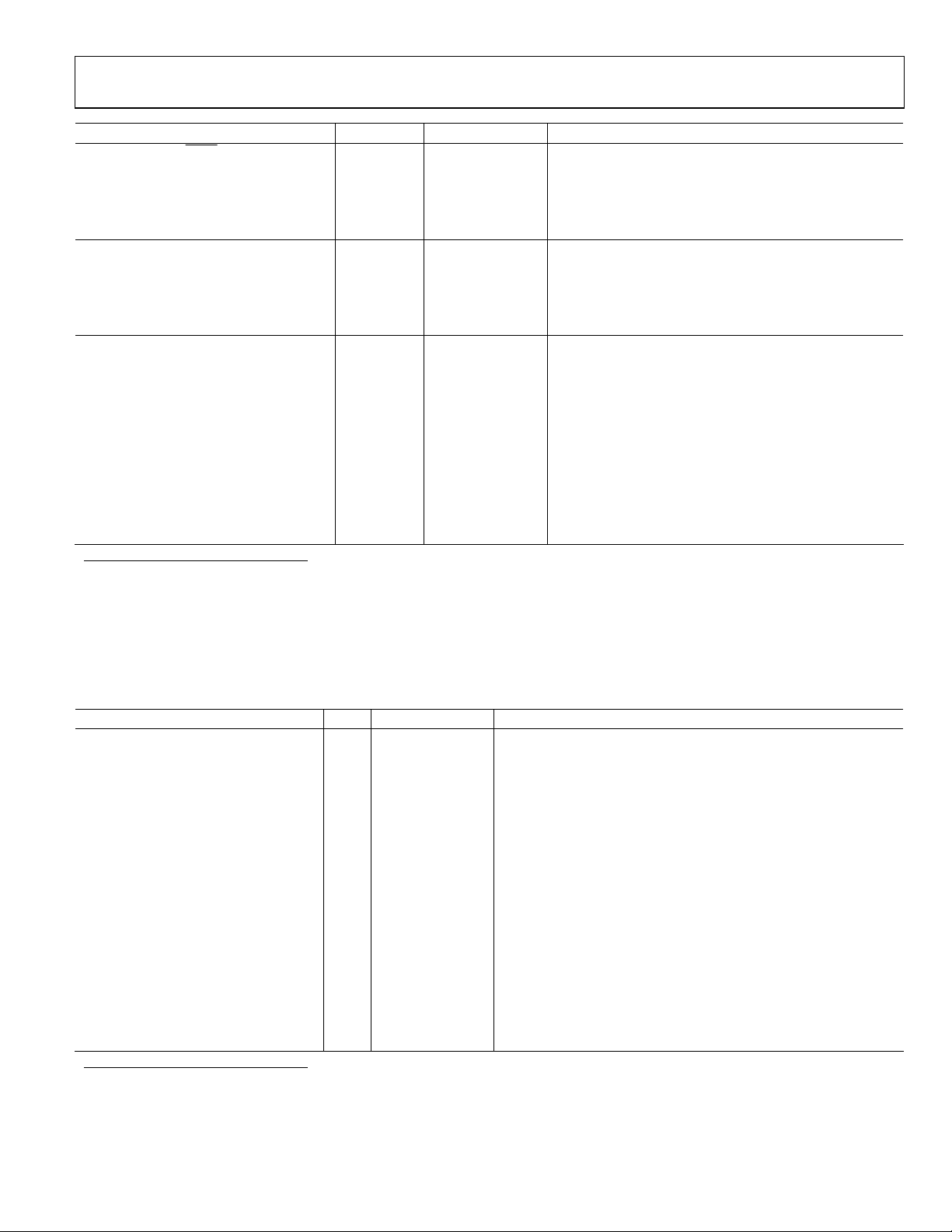
Parameter AD5380-31 Unit Test Conditions/Comments
LOGIC OUTPUTS (BUSY, SDO)3
VOL, Output Low Voltage 0.4 V max Sinking 200 µA
VOH, Output High Voltage DVDD – 0.5 V min Sourcing 200 µA
High Impedance Leakage Current ±1 µA max SDO only
High Impedance Output Capacitance 5 pF typ SDO only
LOGIC OUTPUT (SDA)3
VOL, Output Low Voltage 0.4 V max I
0.6 V max I
Three-State Leakage Current ±1 µA max
Three-State Output Capacitance 8 pF typ
POWER REQUIREMENTS
AVDD 2.7/3.6 V min/max
DVDD 2.7/5.5 V min/max
Power Supply Sensitivity3
∆Midscale/∆ΑVDD –85 dB typ
AIDD 0.375 mA/channel max Outputs unloaded, Boost off. 0.25 mA/channel typ
0.475 mA/channel max Outputs unloaded, Boost on. 0.325 mA/channel typ
DIDD 1 mA max VIH = DVDD, VIL = DGND.
AIDD (Power-Down) 2 µA max Typically 200 nA
DIDD (Power-Down) 20 µA max Typically 3 µA
Power Dissipation 48 mW max Outputs unloaded, Boost off, AVDD = DVDD = 3 V
1
AD5380-3 is calibrated using an external 1.25 V reference. Temperature range is –40°C to +85°C.
2
Accuracy guaranteed from V
3
Guaranteed by characterization, not production tested.
4
Default on the AD5380-3 is 1.25 V. Programmable to 2.5 V via CR12 in the AD5380 control register; operating the AD5380-3 with a 2.5 V reference will lead to degraded
accuracy specifications and limited input code range.
= 10 mV to AVDD – 50 mV.
OUT
= 3 mA
SINK
= 6 mA
SINK
AC CHARACTERISTICS1
Table 5 . AVDD = 2.7 V to 3.6 V and 4.5 V to 5.5 V; DVDD = 2.7 V to 5.5 V; AGND = DGND= 0 V
Parameter All Unit Test Conditions/Comments
DYNAMIC PERFORMANCE
Output Voltage Settling Time 2 1/4 scale to 3/4 scale change settling to ±1 LSB.
8 µs typ
10 µs max
Slew Rate2 2 V/µs typ Boost mode off, CR11 = 0
3 V/µs typ Boost mode on, CR11 = 1
Digital-to-Analog Glitch Energy 12 nV-s typ
Glitch Impulse Peak Amplitude 15 mV typ
Channel-to-Channel Isolation 100 dB typ See Terminology section
DAC-to-DAC Crosstalk 1 nV-s typ See Terminology section
Digital Crosstalk 0.8 nV-s typ
Digital Feedthrough 0.1 nV-s typ Effect of input bus activity on DAC output under test
Output Noise 0.1 Hz to 10 Hz 15 µV p-p typ External reference, midscale loaded to DAC
40 µV p-p typ Internal reference, midscale loaded to DAC
Output Noise Spectral Density
@ 1 kHz 150 nV/√Hz typ
@ 10 kHz 100 nV/√Hz typ
1
Guaranteed by design and characterization, not production tested.
2
The slew rate can be programmed via the current boost control bit (CR11 ) in the AD5380 control register.
Rev. 0 | Page 7 of 40
AD5380
T
TIMING CHARACTERISTICS
SERIAL INTERFACE
Tabl e 6. D VDD= 2.7 V to 5.5 V ; AVDD = 4.5 V to 5.5 V or 2.7 V to 3.6 V; AGND = DGND = 0 V; all specifications
to T
T
MIN
Parameter
t1 33 ns min SCLK cycle time
t2 13 ns min SCLK high time
t3 13 ns min SCLK low time
t4 13 ns min
t5 4 13 ns min
4
t
33 ns min
6
t7 10 ns min
t7A 50 ns min
t8 5 ns min Data setup time
t9 4.5 ns min Data hold time
4
t
30 ns max
10
t11 670 ns max
4
t
20 ns min
12
t13 20 ns min
t14 100 ns max
t15 0 ns min
t16 100 ns min
t17 8 µs typ DAC output settling time
t18 20 ns min
t
35 µs max
19
5
t
20 ns max SCLK rising edge to SDO valid
20
5
t
5 ns min
21
5
t
8 ns min
22
t23 20 ns min
, unless otherwise noted
MAX
1, 2, 3
Limit at T
MIN
, T
Unit Description
MAX
falling edge to SCLK falling edge setup time
SYNC
th
SCLK falling edge to SYNC falling edge
24
Minimum SYNC
Minimum SYNC
Minimum SYNC
24th SCLK falling edge to BUSY
pulse width low (single channel update)
BUSY
24th SCLK falling edge to LDAC
pulse width low
LDAC
rising edge to DAC output response time
BUSY
rising edge to LDAC falling edge
BUSY
falling edge to DAC output response time
LDAC
pulse width low
CLR
pulse activation time
CLR
SCLK falling edge to SYNC
rising edge to SCLK rising edge
SYNC
rising edge to LDAC falling edge
SYNC
low time
high time
high time in Readback mode
falling edge
falling edge
rising edge
1
Guaranteed by design and characterization, not production tested.
2
All input signals are specified with t
3
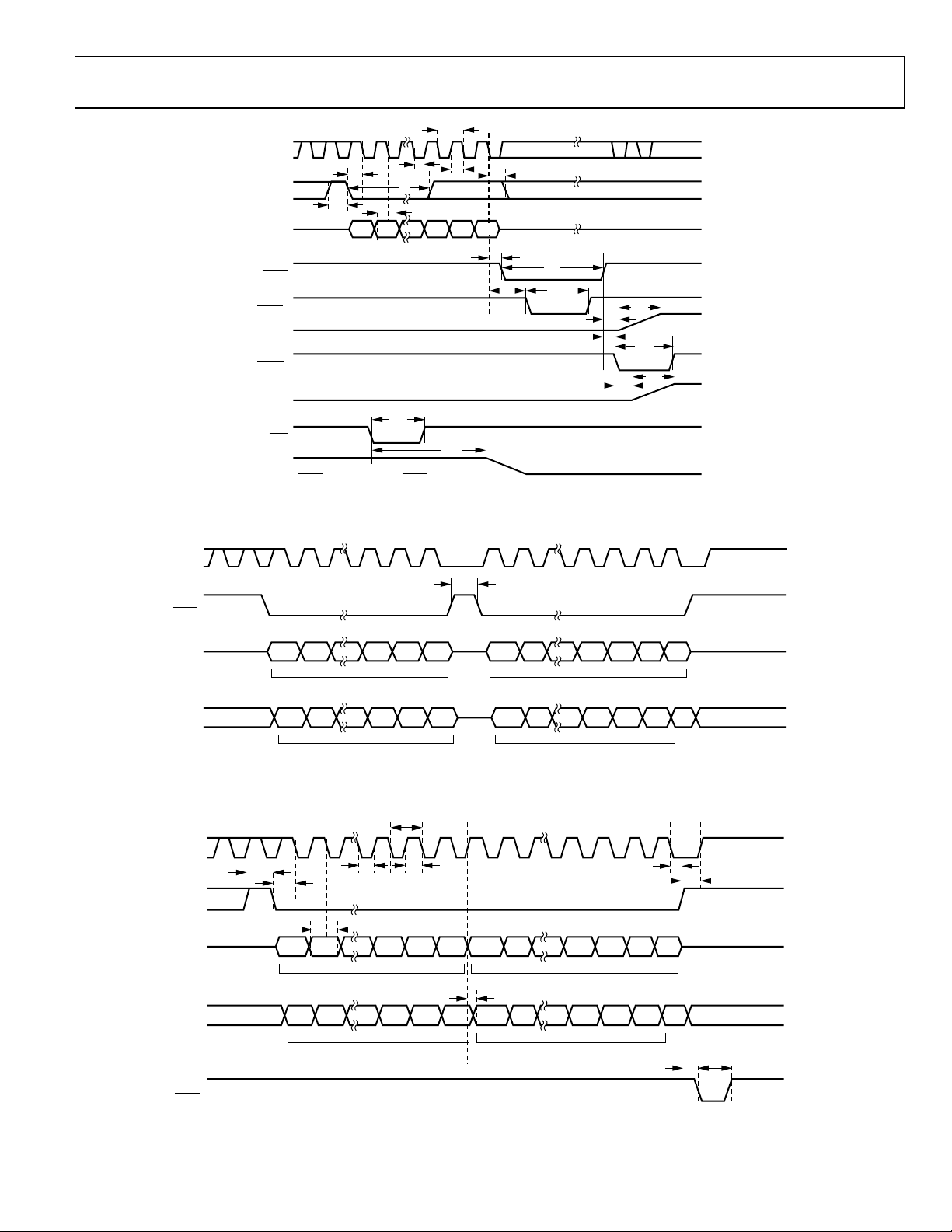
See Figure 2, Figure 3, Figure 4, and Figure 5.
4
Standalone mode only.
5
Daisy-chain mode only.
= t
= 5 ns (10% to 90% of VCC), and are timed from a voltage level of 1.2 V.
r
f
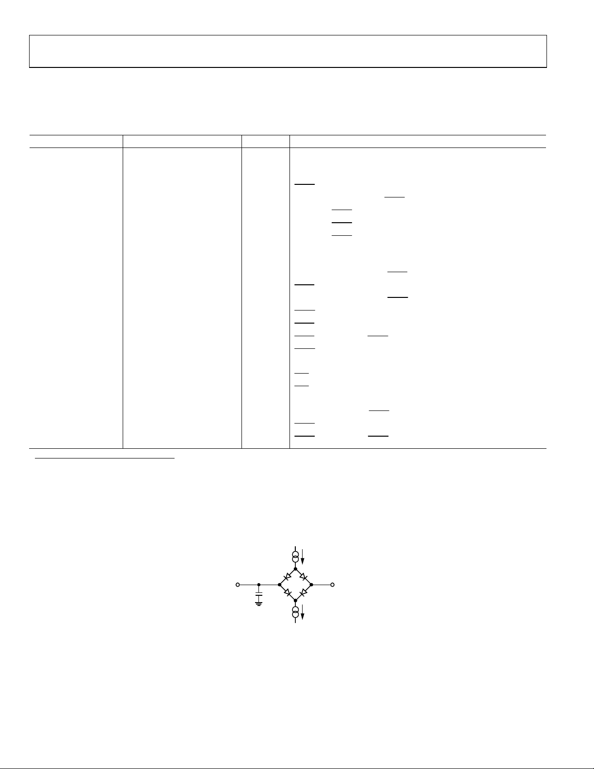
O OUTPUT PIN
Figure 2. Load Circuit for Digital Output Timing
C
L
50pF
200µA
200µA
I
OL
I
OH
Rev. 0 | Page 8 of 40
V
OH
V
OL
(MIN) OR
(MAX)
03731-0-003
AD5380
t
1
SCLK
t
3
t
4
t
SYNC
DIN
t
7
DB23
t8t
6
9
BUSY
1
LDAC
1
V
OUT
2
LDAC
2
V
OUT
t
18
CLR
V
OUT
1
LDAC ACTIVE DURING BUSY
2
LDAC ACTIVE AFTER BUSY
Figure 3. Serial Interface Timing Diagram (Standalone Mode)
t
2
t
5
DB0
t
10
t
11
t
t
19
t
12
13
t
15
24 48SCLK
t
7A
SYNC
2424
t
17
t
14
t
13
t
17
t
16
03731-0-004
DIN
SDO
SCLK
DB23 DB0 DB23 DB0
INPUT WORD SPECIFIES
REGISTER TO BE READ
NOP CONDITION
DB23 DB0
UNDEFINED
SELECTED REGISTER
DATA CLOCKED OUT
Figure 4. Serial Interface Timing Diagram (Data Readback Mode)
t
1
t
7
t
4
t
t
3
2
t
03731-0-005
4824
21
t
22
SYNC
t8t
9
DIN
DB23 DB0 DB0DB23
INPUT WORD FOR DAC N INPUT WORD FOR DAC N+1
t
20
SDO
UNDEFINED INPUT WORD FOR DAC N
LDAC
Figure 5. Serial Interface Timing Diagram (Daisy-Chain Mode)
DB23 DB0
t
13
t
23
03731-0-006
Rev. 0 | Page 9 of 40
AD5380
I2C SERIAL INTERFACE
Tabl e 7. D VDD = 2.7 V to 5.5 V; AVDD = 4.5 V to 5.5 V or 2.7 V to 3.6 V; AGND = DGND = 0 V; all specifications
to T
T
MIN
Parameter
F
400 kHz max SCL clock frequency
SCL
t1 2.5 µs min SCL cycle time
t2 0.6 µs min t
t3 1.3 µs min t
t4 0.6 µs min t
t5 100 ns min t
3
t
0.9 µs max t
6
0 µs min t
t7 0.6 µs min t
t8 0.6 µs min t
t9 1.3 µs min t
t10 300 ns max tR, rise time of SCL and SDA when receiving
0 ns min tR, rise time of SCL and SDA when receiving (CMOS compatible)
t11 300 ns max tF, fall time of SDA when transmitting
0 ns min tF, fall time of SDA when receiving (CMOS compatible)
300 ns max tF, fall time of SCL and SDA when receiving
20 + 0.1Cb 4 ns min tF, fall time of SCL and SDA when transmitting
Cb 400 pF max Capacitive load for each bus line
1
Guaranteed by design and characterization, not production tested.
2
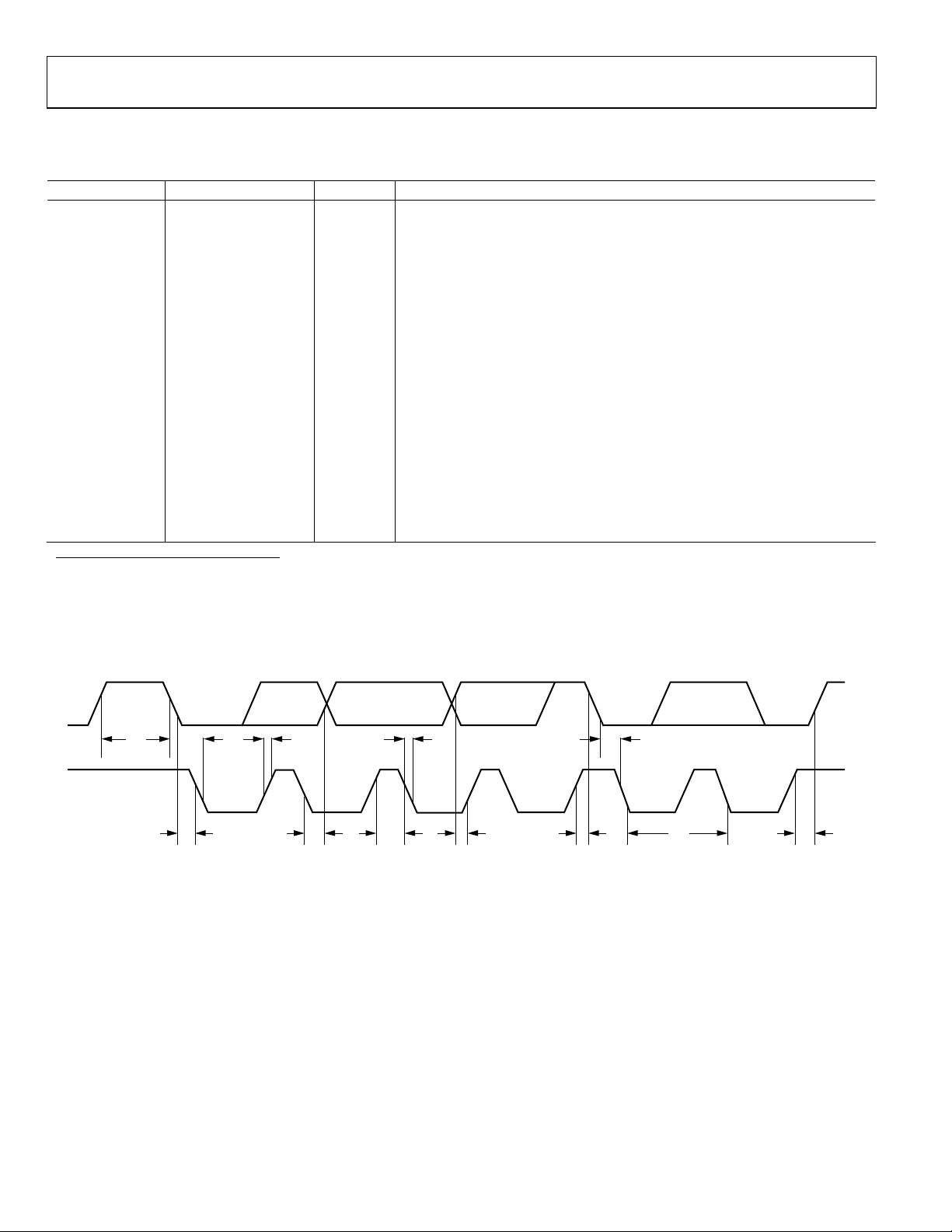
See Figure 6.
3
A master device must provide a hold time of at least 300 ns for the SDA signal (referred to the V
falling edge.
4
Cb is the total capacitance, in pF, of one bus line. tR and tF are measured between 0.3 DVDD and 0.7 DVDD.
, unless otherwise noted
MAX
1, 2
Limit at T
MIN
, T
Unit Description
MAX
, SCL high time
HIGH
, SCL low time
LOW
, start/repeated start condition hold time
HD,STA
, data setup time
SU,DAT
, data hold time
HD,DAT
, data hold time
HD,DAT
, setup time for repeated start
SU,STA
, stop condition setup time
SU,STO
, bus free time between a STOP and a START condition
BUF
min of the SCL signal) in order to bridge the undefined region of SCL’s
IH
SDA
SCL
t
9
START
CONDITION
t
3
t
4
t
10
t
6
Figure 6. I
t
2
C Compatible Serial Interface Timing Diagram
t
11
2
t
5
REPEATED
CONDITION
t
7
START
t
4
t
1
t
8
STOP
CONDITION
03731-0-007
Rev. 0 | Page 10 of 40
AD5380
PARALLEL INTERFACE
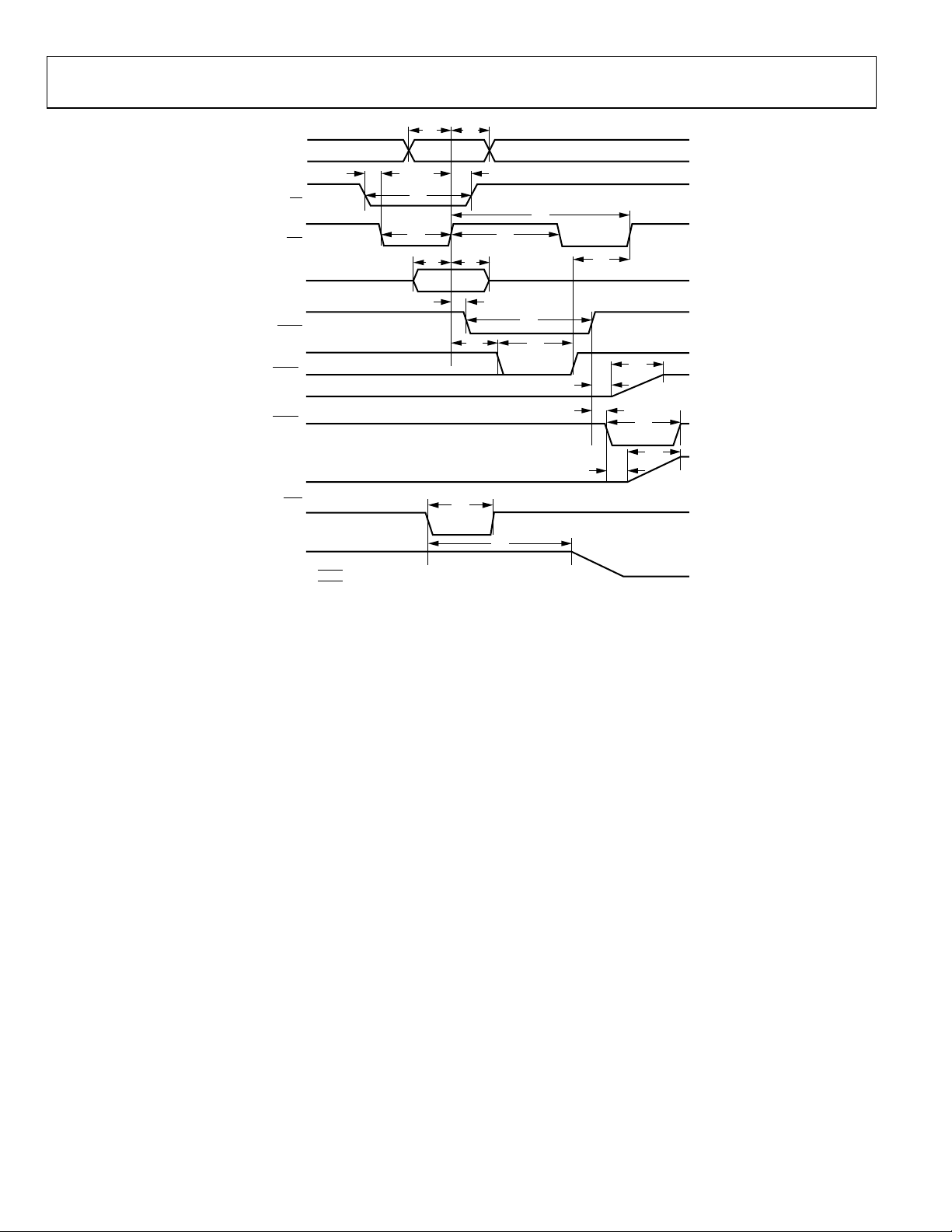
Tabl e 8. D VDD = 2.7 V to 5.5 V; AVDD = 4.5 V to 5.5 V or 2.7 V to 3.6 V; AGND = DGND = 0 V; all specifications
to T
T
MIN
Parameter
t0 4.5 ns min
t1 4.5 ns min
t2 20 ns min
t3 20 ns min
t4 0 ns min
t5 0 ns min
t6 4.5 ns min
t7 4.5 ns min
t8 20 ns min
4
t
700 ns min
9
t10 30 ns max
4
t
670 ns max
11
t12 30 ns min
t13 20 ns min
t14 100 ns max
t15 20 ns min
t16 0 ns min
t17 100 ns min
t18 8 µs typ DAC output settling time
t19 20 ns min
t20 35 µsmax
1
Guaranteed by design and characterization, not production tested.
2
All input signals are specified with tR = tR = 5 ns (10% to 90% of DVDD) and timed from a voltage level of 1.2 V.
3
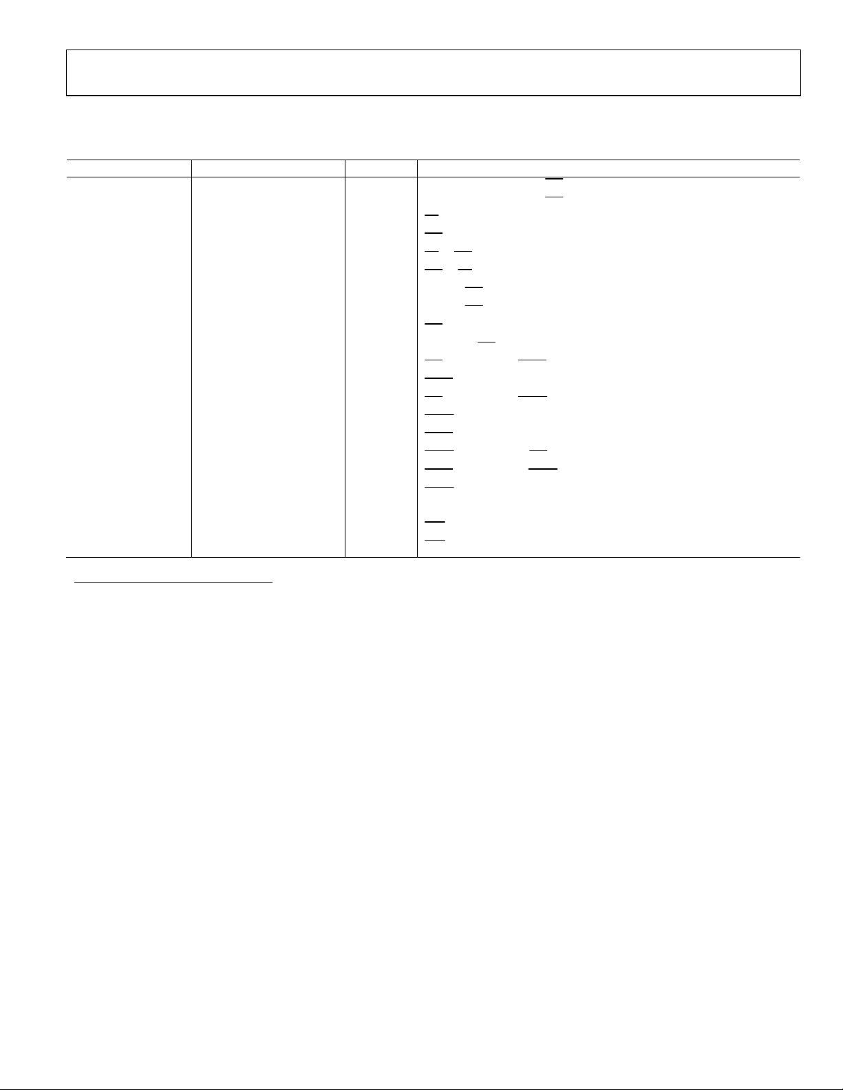
See Figure 7.
4
See Figure 29.
, unless otherwise noted
MAX
1,2,3
Limit at T
MIN
, T
Unit Description
MAX
REG0, REG1, address to WR
REG0, REG1, address to WR
pulse width low
CS
pulse width low
WR
to WR falling edge setup time
CS
to CS rising edge hold time
WR
Data to WR
Data to WR
WR
rising edge setup time
rising edge hold time
pulse width high
Minimum WR
rising edge to BUSY falling edge
WR
pulse width low (single-channel update)
BUSY
rising edge to LDAC falling edge
WR
pulse width low
LDAC
rising edge to DAC output response time
BUSY
rising edge to WR rising edge
LDAC
rising edge to LDAC falling edge
BUSY
falling edge to DAC output response time
LDAC
pulse width low
CLR
pulse activation time
CLR
rising edge setup time
rising edge hold time
cycle time (single-channel write)
Rev. 0 | Page 11 of 40
AD5380
t
t
0
1
REG0, REG1, A5..A0
WR
DB13..DB0
BUSY
LDAC
V
OUT
LDAC
V
OUT
CLR
V
OUT
CS
1
1
2
2
t
4
t
5
t
2
t
9
t
3
t
6
t
t
t
8
t
t
7
10
t
11
t
12
19
t
13
t
20
15
t
18
t
14
t
16
t
13
t
18
t
17
1
LDAC ACTIVE DURING BUSY
2
LDAC ACTIVE AFTER BUSY
03731-0-008
Figure 7. Parallel Interface Timing Diagram
Rev. 0 | Page 12 of 40
 Loading...