

查询AD5231供应商查询AD5231供应商
PRELIMINARY TECHNICAL DATA
a
FEATURES
Nonvolatile Memory Preset Maintains Wiper Settings
AD5231 Single, 1024 Position Resolution
AD5232 Dual, 256 Position Resolution
AD5233 Quad, 64 Position Resolution
10K, 50K, 100K Ohm Terminal Resistance
Linear or Log taper Settings
Increment/Decrement Commands, Push Button Command
SPI Compatible Serial Data Input with Readback Function
+3 to +5V Single Supply or ±2.5V Dual Supply Operation
User EEMEM nonvolatile memory for constant storage
APPLICATIONS
Mechanical Potentiometer Replacement
Instrumentation: Gain, Offset Adjustment
Programmable Voltage to Current Conversion
Programmable Filters, Delays, Time Constants
Line Impedance Matching
Power Supply Adjustment
DIP Switch Setting
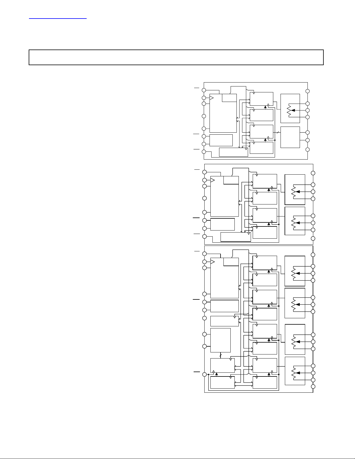
GENERAL DESCRIPTION
The AD5231/AD5232/AD5233 family provides a single/dual-/quad-channel, digitally controlled variable resistor (VR)
with resolutions of 1024/256/64 positions respectively. These
devices perform the same electronic adjustment function as a
potentiometer or variable resistor. The AD523X’s versatile
programming via a Micro Controller allows multiple modes of
operation and adjustment.
In the direct program mode a predetermined setting of the
RDAC register can be loaded directly from the micro controller.
Another key mode of operation allows the RDAC register to be
refreshed with the setting previously stored in the EEMEM
register. When changes are made to the RDAC register to
establish a new wiper position, the value of the setting can be
saved into the EEMEM by executing an EEMEM save
operation. Once the settings are saved in the EEMEM register
these values will be transferred automatically to the RDAC
register to set the wiper position at system power ON. Such
operation is enabled by the internal preset strobe and the preset
can also be accessed externally.
The basic mode of adjustment is the increment and decrement
command controlling the present setting of the Wiper position
setting (RDAC) register. An internal scratch pad RDAC register
can be moved UP or DOWN, one step of the nominal terminal
resistance between terminals A-and-B. This linearly changes the
wiper to B terminal resistance (R
the device's end-to-end resistance (RAB). For
exponential/logarithmic changes in wiper setting, a left/right
shift command adjusts levels in +/-6dB steps, which can be
useful for sound and light alarm applications.
The AD523X are available in the thin TSSOP package. All
parts are guaranteed to operate over the extended industrial
temperature range of -40°C to +85°C.
REV PrF, 22 MAR '01
Information fur nished by Analog Devices is believed to be acc urate and reliable. However, no
responsibility is assumed by Analog Devices for its use; nor for any infringements of patents
or other rights of third parties, which may result from its use. No license is granted by
implication or otherwise under any patent or patent rights of Analog Devices.
) by one position segment of
WB
Nonvolatile Memory
Digital Potentiometers
AD5231/AD5232/AD5233
FUNCTIONAL BLOCK DIAGRAMS
CS
CLK
SDI
GND
SDO
WP
RDY
PR
CS
CLK
SDI
GND
SDO
WP
RDY
PR
CS
CLK
SDI
SDO
WP
RDY
GND
O
1
O
2
PR
One Technology Way, P.O. Box 9106,
Tel: 781/329-4700 World Wide Web Site: http://www.analog.com
Fax:617/326-8703 © Analog Devices, Inc., 1999
ADDR
DECODE
SDI
SERIAL
INT E RF A CE
SDO
EEMEM
CONTROL
28 BYTE S
USER EEMEM
ADDR
DECODE
SDI
SERIAL
INT E RF A CE
SDO
EEMEM
CONTROL
14 BYTES
USER EEMEM
ADDR
DECODE
SDI
SERIAL
INT E RF A CE
SDO
EEMEM
CONTROL
11 BYT ES
USER EEMEM
DIGITAL
OUTPUT
BUFFER
2
DIGITAL 5
REGISTER
EEMEM5
RDAC1
REGISTER
EEMEM1
DIGITAL 2
REGISTER
EEMEM2
RDAC1
REGISTER
EEMEM1
RDAC2
REGISTER
EEMEM2
RDAC1
REGISTER
EEMEM1
RDAC2
REGISTER
EEMEM2
RDAC3
REGISTER
EEMEM3
RDAC4
REGISTER
EEMEM4
Norwood, MA 02062-9106 U.S.A.
AD5231
RDAC1
DIGITAL
2
OUTPUT
BUFFER
AD5232
RDAC1
RDAC2
AD5233
RDAC1
RDAC2
RDAC3
RDAC4
V
DD
A
1
W
1
B
1
O
1
O
2
V
SS
V
DD
A
1
W
1
B
1
A
2
W
2
B
2
V
SS
V
DD
A
1
W
1
B
1
A
2
W
2
B
2
A
3
W
3
B
3
A
4
W
4
B
4
V
SS

PRELIMINARY TECHNICAL DATA
AD5231/AD5232/AD5233 -
SPECIFICATIONS
ELECTRICAL CHARACTERISTICS 10K, 50K, 100K OHM VERSIONS
= +VDD, VB = 0V, -40°C < TA < +85°C unless otherwise noted.)
V
A
(VDD = +3V±10% or +5V±10% and VSS=0V,
Parameter Symbol Conditions Min Typ1 Max Units
DC CHARACTERISTICS RHEOSTAT MODE Specifications apply to all VRs
Resistor Differential Nonlinearity2 R-DNL RWB, VA=NC -1 ±1/4 +1 LSB
Resistor Nonlinearity2 R-INL RWB, VA=NC -1 ±1/2 +1 %FS
Nominal resistor tolerance ∆R TA = 25°C, VAB = VDD,Wiper (VW) = No connect -30 30 %
Resistance Temperature Coefficent RAB/∆T V
Wiper Resistance RW I
Wiper Resistance RW I
= VDD, Wiper (VW) = No Connect 500 ppm/°C
AB
= 1 V/R, VDD = +5V 50 100 Ω
W
= 1 V/R, VDD = +3V 200 Ω
W
DC CHARACTERISTICS POTENTIOMETER DIVIDER MODE Specifications apply to all VRs
Resolution N AD5231/AD5232/AD5233 10 / 8 / 6 Bits
Integral Nonlinearity3 INL –1 ±1/2 +1 %FS
Differential Nonlinearity3 DNL –1 ±1/4 +1 LSB
Voltage Divider Temperature Coefficent ∆VW/∆T Code = Half-scale 15 ppm/°C
Full-Scale Error V
Zero-Scale Error V
Code = Full-scale –3 +0 %FS
WFSE
Code = Zero-scale 0 +3 %FS
WZSE
RESISTOR TERMINALS
Voltage Range4 V
Capacitance5 Ax, Bx C
VSS V
A,B,W
f = 1 MHz, measured to GND, Code = Half-scale 45 pF
A,B
V
DD
Capacitance5 Wx CW f = 1 MHz, measured to GND, Code = Half-scale 60 pF
Common-mode Leakage Current6 I
V
CM
= VB = VDD/2 0.01 1 µA
A
DIGITAL INPUTS & OUTPUTS
Input Logic High VIH with respect to GND, VDD = 5V 2.4 V
Input Logic Low VIL with respect to GND, VDD = 5V 0.8 V
Input Logic High VIH with respect to GND, VDD = 3V 2.1 V
Input Logic Low VIL with respect to GND, VDD = 3V 0.6 V
Output Logic High VOH R
Output Logic High VOH IOH = 40µA, V
Output Logic Low VOL I
Input Current IIL V
Input Capacitance5 C
5 pF
IL
= 2.2KΩ to +5V 4.9 V
PULL-UP
= +5V 4 V
= 1.6mA, V
OL
= 0V or VDD ±1 µA
IN
LOGIC
= +5V 0.4 V
LOGIC
POWER SUPPLIES
Single-Supply Power Range VDD V
= 0V 2.7 5.5 V
SS
Dual-Supply Power Range VDD/VSS ±2.25 ±2.75 V
Positive Supply Current IDD V
Programming Mode Current I
Read Mode Current13 I
VIH = VDD or VIL = GND 35 mA
DD(PG)
DD(READ)
Negative Supply Current ISS V
Power Dissipation7 P
V
DISS
= VDD or VIL = GND 2 20 µA
IH
VIH = VDD or VIL = GND 0.9 9 mA
= VDD or VIL = GND, V
IH
= VDD or VIL = GND 0.1 mW
IH
= 2.5V, V
DD
= -2.5V 10 µA
SS
Power Supply Sensitivity PSS ∆VDD = +5V ±10% 0.002 0.01 %/%
DYNAMIC CHARACTERISTICS
5, 8
Bandwidth –3dB BW_10K R = 10KΩ 600 KHz
Total Harmonic Distortion THDW V
VW Settling Time tS V
=1Vrms, VB = 0V, f=1KHz 0.003 %
A
= VDD, VB=0V, 50% of final value
A
For RAB = 10K/50K/100K 1 / 3 / 6 µs
Resistor Noise Voltage e
Crosstalk (CW1/CW2) CT V
RWB = 5KΩ, f = 1KHz 9 nV√Hz
N_WB
= VDD, VB = 0V, Measure VW with adjacent
A
VR making full scale change -65 dB
NOTES: See bottom of table next page.
REV PrF 2 22 MAR '01
Information contained in this Preliminary data sheet describes a product in the early definition stage. There is no guarantee that the
information contained here will become a final product in its present form. For latest information contact Walt Heinzer/Analog Devices, Santa
Clara, CA. TEL(408)382-3107; FAX (408)382-2708; walt.heinzer@analog.com
PRELIMINARY TECHNICAL DATA
AD5231/AD5232/AD5233 -
SPECIFICATIONS
ELECTRICAL CHARACTERISTICS 10K, 50K, 100K OHM VERSIONS
V
= +VDD, VB = 0V, -40°C < TA < +85°C unless otherwise noted.)
A
Parameter Symbol Conditions Min Typ1 Max Units
(VDD = +3V±10% to +5V±10% and VSS=0V,
INTERFACE TIMING CHARACTERISTICS applies to all parts(Notes 5, 9)
Clock Cycle Time t 1 20 ns
Input Clock Pulse Width t 2 , t 3 Clock level high or low 10 ns
CS Setup Time t
10 ns
4
Data Setup Time t 5 From Positive CLK transition 5 ns
Data Hold Time t 6 From Positive CLK transition 5 ns
CLK Shutdown Time t 7 0 ns
CS Rise to Clock Rise Setup t
CS High Pulse Width t
CLK to SDO Propagation Delay10 t
10 ns
8
10 ns
9
RP = 1KΩ, CL < 20pF 1 25 ns
10
Store to Nonvolatile EEMEM Save Time11 t 12 Applies to Command 2H, 3H, 9H 25 ms
CS to SDO - SPI line acquire t
CS to SDO - SPI line release t
ns
13
ns
14
RDY Rise to CS Fall t15 ns
Startup Time t16 ms
CLK Setup Time t17 For 1 CLK period (t4 - t3 = 1 CLK period) ns
Preset Pulse Width (Asynchronous) tPR 50 ns
Preset Response Time t
PR pulsed low then high 70 us
PRESP
NOTES:
1. Typicals represent average readings at +25°C and VDD = +5V.
2. Resistor position nonlinearity error R-INL is the deviation from an ideal value measured between the maximum resistance and the minimum resistance wiper positions. R-DNL measures the
relative step c hange from ideal between successive tap positions. Parts are guaranteed monotonic. I
3. INL and DNL are measured at V
DNL specification limits of ±1LSB maximum are Guaranteed Monotonic operating conditions.
4. Resistor terminals A, B, W have no limitations on polarity with respect to each other.
5. Guaranteed by design and not subject to production test.
6. Common mode leakage current is a measure of the DC leakage from any terminal A, B, W to a common mode bias level of V
7. P
8. All dynamic char acteristics use V
9. See timing diagram for location of measured values. All input control voltages are specified with t
10. Propagation delay depends on value of V
11. Low only for instruction commands 8, 9,10, 2, 3: CMD_8 ~ 1ms; CMD_9,10 ~0.12ms; CMD_2,3 ~20ms
12. Dual Supply Operation primarily affects the POT terminals.
13. Read Mode current is not continuous.
is calculated from (IDD x VDD) + (ISS X VSS).
DISS
characteristics are measur ed using both V
with the RDA C configured as a potentiometer divider similar to a voltage output D/A converter. VA = VDD and VB = VSS.
W
= +5V.
DD
= +3V or +5V.
DD
, R
DD
PULL_UP
, and CL see applications text.
= VDD/R for both VDD=+3V or VDD=+5V.
W
/ 2.
DD
=2.5ns(10% to 90% of 3V) and timed from a voltage level of 1.5V. Switching
R=tF
Timing Diagram
CLK
t
17
t
4
t
1
CS
t
5
SDI
SDO
SDO
t
13
1
2
t
MSB LSB
t
10
MSB LSB
MSB LSB
15
RDY
SDO1 CLK IDLES LOW SDO2 CLK IDLES HIGH
Figure 1. Timing Diagram
REV PrF 3 22 MAR '01
Information contained in this Preliminary data sheet describes a product in the early definition stage. There is no guarantee that the
information contained here will become a final product in its present form. For latest information contact Walt Heinzer/Analog Devices, Santa
Clara, CA. TEL(408)382-3107; FAX (408)382-2708; walt.heinzer@analog.com
t
t
2
3
t
7
t
6
t
8
t
9
t
14
t
16
t
12

PRELIMINARY TECHNICAL DATA
Nonvolatile Memory Digital Potentiometers
Absolute Maximum Rating (
TA = +25°C, unless
otherwise noted)
V
to GND..............................................................-0.3, +7V
DD
to GND .................................................................0V, -7V
V
SS
to VSS.........................................................................+7V
V
DD
, VB, VW to GND..................................................VSS, VDD
V
A
A
– BX, AX – WX, BX – W
X
X
Intermittent ...................................................±20mA
Continuous................................................... ±1.3mA
Digital Inputs & Output Voltage to GND .................. 0V, +7V
Operating Temperature Range ........................ -40°C to +85°C
Maximum Junction Temperature (T
Storage Temperature..................................... -65°C to +150°C
Lead Temperature (Soldering, 10 sec) .........................+300°C
Package Power Dissipation........................ (T
Thermal Resistance θ
TSSOP-16 ..................................................... 150°C/W
TSSOP-24 ..................................................... 128°C/W
AD5231/AD5232/AD5233
) ..................+150°C
MAX
J
- TA) /
θ
JA
JA,
MAX
J
Ox to GND .................................................................. 0V, VDD
Ordering Guide
Number of End to End Temp Package Package #Devices Top Mark
Model Channels R (k Ohm) Range Description Option per Container
AD5231BRU10 X1 10 -40/+85°C TSSOP-16 RU-16
AD5231BRU10-REEL7 X1 10 -40/+85°C TSSOP-16 RU-16 1,000
AD5231BRU50 X1 50 -40/+85°C TSSOP-16 RU-16
AD5231BRU50-REEL7 X1 50 -40/+85°C TSSOP-16 RU-16 1,000
AD5231BRU100 X1 100 -40/+85°C TSSOP-16 RU-16
AD5231BRU100-REEL7 X1 100 -40/+85°C TSSOP-16 RU-16 1,000
AD5232BRU10 X2 10 -40/+85°C TSSOP-16 RU-16
AD5232BRU10-REEL7 X2 10 -40/+85°C TSSOP-16 RU-16 1,000
AD5232BRU50 X2 50 -40/+85°C TSSOP-16 RU-16
AD5232BRU50-REEL7 X2 50 -40/+85°C TSSOP-16 RU-16 1,000
AD5232BRU100 X2 100 -40/+85°C TSSOP-16 RU-16
AD5232BRU100-REEL7 X2 100 -40/+85°C TSSOP-16 RU-16 1,000
AD5233BRU10 X4 10 -40/+85°C TSSOP-24 RU-24
AD5233BRU10-REEL7 X4 10 -40/+85°C TSSOP-24 RU-24
AD5233BRU50 X4 50 -40/+85°C TSSOP-24 RU-24
AD5233BRU50-REEL7 X4 50 -40/+85°C TSSOP-24 RU-24
AD5233BRU100 X4 100 -40/+85°C TSSOP-24 RU-24
AD5233BRU100-REEL7 X4 100 -40/+85°C TSSOP-24 RU-24
The AD5231/AD5232/AD5233 contains 9,646 transistors.
Die size: 69 mil x 115 mil, 7,993 sq. mil
REV PrF 4 22 MAR '01
Information contained in this Preliminary data sheet describes a product in the early definition stage. There is no guarantee that the
information contained here will become a final product in its present form. For latest information contact Walt Heinzer/Analog Devices, Santa
Clara, CA. TEL(408)382-3107; FAX (408)382-2708; walt.heinzer@analog.com

PRELIMINARY TECHNICAL DATA
Nonvolatile Memory Digital Potentiometers
AD5231
PIN CONFIGURATION
O1
CLK
SDI
SDO
GND
V
B1
1
2
3
4
5
6
SS
7
T1
8
O2
16
15
RDY
14
CS
CS
CSCS
13
PR
PR
PRPR
12
WP
WP
WPWP
11
V
DD
10
A1
9
W1
AD5231 PIN FUNCTION DESCRIPTION
# Name Description
1 O1 Non-Volatile Digital Output #1, ADDR(O1) =
1H, data bit position D0
2 CLK Serial Input Register clock pin. Shifts in one
bit at a time on positive clock CLK edges.
3 SDI Serial Data Input Pin.
4 SDO Serial Data Output Pin. Open Drain Output
requires external pull-up resistor. Commands 9
& 10 activate the SDO output. See Instruction
operation Truth Table. Other commands shift
out the previously loaded bit pattern delayed
by 24 clock pulses. This allows daisy-chain
operation of multiple packages.
5 GND Ground pin, logic ground reference.
6 V
7 T1 Used as digital input during factory test mode.
8 B1 B terminal of RDAC1.
9 W1 Wiper terminal of RDAC1,
10 A1 A terminal of RDAC1.
11 VDD Positive Power Supply Pin. Should be ≥ the
12 WP Write Protect Pin. When active low WP
13 PR Hardware over ride preset pin. Refreshes the
14 CS Serial Register chip select active low. Serial
15 RDY Ready. Active-high open drain output.
16 O2 Non-Volatile Digital Output #2, ADDR(O2) =
Negative Supply. Connect to zero volts for
SS
single supply applications.
Leave pin floating or connect to V
ADDR(RDAC1) = 0
H
or VSS.
DD
input-logic HIGH voltage.
prevents any changes to the present contents
except retrieving EEMEM contents and
RESET.
scratch pad register with current contents of
the EEMEM register. Factory default loads
midscale 200
until EEMEM loaded with a
H
new value by the user (PR is activated at the
rising logic high transition)
register operation takes place when CS returns
to logic high.
Identifies completion of commands 2, 3, 8, 9,
10.
1H, data bit position D1.
AD5232 PIN FUNCTION DESCRIPTION
# Name Description
1 CLK Serial Input Register clock pin. Shifts in one
2 SDI Serial Data Input Pin. Shifts in one bit at a
3 SDO Serial Data Output Pin. Open Drain Output
4 GND Ground pin, logic ground reference
5 V
6 A1 A terminal of RDAC1.
7 W1 Wiper terminal of RDAC1,
8 B1 B terminal of RDAC1.
9 B2 B terminal of RDAC2.
10 W2 Wiper terminal of RDAC2,
11 A2 A terminal of RDAC2.
12 V
13 WP Write Protect Pin. When active low, WP
14 PR Hardware over ride preset pin. Refreshes the
15 CS Serial Register chip select active low. Serial
16 RDY Ready. Active-high open drain output.
AD5231/AD5232/AD5233
AD5232
Negative Supply. Connect to zero volts for
SS
Positive Power Supply Pin. Should be ≥ the
DD
PIN CONFIGURATION
CLK
1
2
SDI
3
SDO
4
GND
5
V
SS
6
A1
7
W1
8
B1
bit at a time on positive clock edges.
time on positive clock CLK edges.
requires external pull-up resistor. Commands 9
& 10 activate the SDO output. See Instruction
operation Truth Table. Other commands shift
out the previously loaded bit pattern delayed
by 16 clock pulses. This allows daisy-chain
operation of multiple packages.
single supply applications.
ADDR(RDAC1) = 0
ADDR(RDAC2) = 1H.
input-logic HIGH voltage.
prevents any changes to the present contents,
except retrieving EEMEM content and
RESET.
scratch pad register with current contents of
the EEMEM register. Factory default loads
midscale 80
until EEMEM loaded with a new
H
value by the user (PR is activated at the logic
high transition).
register operation takes place when CS returns
to logic high.
Identifies completion of commands 2, 3, 8, 9,
10.
RDY
16
15
CS
CS
CSCS
14
PR
PR
PRPR
13
WP
WP
WPWP
12
V
DD
11
A2
10
W2
9
B2
.
H
REV PrF 5 22 MAR '01
Information contained in this Preliminary data sheet describes a product in the early definition stage. There is no guarantee that the
information contained here will become a final product in its present form. For latest information contact Walt Heinzer/Analog Devices, Santa
Clara, CA. TEL(408)382-3107; FAX (408)382-2708; walt.heinzer@analog.com

PRELIMINARY TECHNICAL DATA
Nonvolatile Memory Digital Potentiometers
AD5231/AD5232/AD5233
AD5233
CLK
SDO
GND
PIN CONFIGURATION
24
O2
23
RDY
CS
CS
22
CSCS
PR
PR
21
PRPR
WP
WP
WPWP
20
V
19
DD
A4
18
W4
17
B4
16
A3
15
W3
14
B3
13
SDI
V
W1
W2
O1
1
2
3
4
5
6
SS
A1
7
8
B1
9
A2
10
11
B2
12
AD5233 PIN FUNCTION DESCRIPTION
# Name Description
1 O1 Non-Volatile Digital Output #1, ADDR(O1) = 4H, data bit position D0.
2 CLK Serial Input Register clock pin. Shifts in one bit at a time on positive clock CLK edges.
3 SDI Serial Data Input Pin.
4 SDO Serial Data Output Pin. Open Drain Output requires external pull-up resistor. Commands 9 & 10 activate the SDO output.
See Instruction operation Truth Table. Other commands shift out the previously loaded bit pattern delayed by 16 clock
pulses. This allows daisy-chain operation of multiple packages.
5 GND Ground pin, logic ground reference
6 VSS Negative Supply. Connect to zero volts for single supply applications.
7 A1 A terminal of RDAC1.
8 W1 Wiper terminal of RDAC1, ADDR(RDAC1) = 0
9 B1 B terminal of RDAC1.
10 A2 A terminal of RDAC2.
11 W2 Wiper terminal of RDAC2, ADDR(RDAC2) = 1H.
12 B2 B terminal of RDAC2.
13 B3 B terminal of RDAC3.
14 W3 Wiper terminal of RDAC3, ADDR(RDAC3) = 2
15 A3 A terminal of RDAC3.
16 B4 B terminal of RDAC4.
17 W4 Wiper terminal of RDAC4, ADDR(RDAC4) = 3
18 A4 A terminal of RDAC4.
19 V
Positive Power Supply Pin. Should be ≥ the input-logic HIGH voltage.
DD
20 WP Write Protect Pin. When active low, WP prevents any changes to the present contents, except retrieving EEMEM content
and RESET.
21 PR Hardware over ride preset pin. Refreshes the scratch pad register with current contents of the EEMEM register. Factory
default loads midscale 20
until EEMEM loaded with a new value by the user (PR is activated at the logic high
H
transition).
22 CS Serial Register chip select active low. Serial register operation takes place when CS returns to logic high.
23 RDY Ready. Active-high open drain output. Identifies completion of commands 2, 3, 8, 9, 10.
24 O2 Non-Volatile Digital Output #2, ADDR(O2) = 4
.
H
.
H
.
H
, data bit position D1.
H
REV PrF 6 22 MAR '01
Information contained in this Preliminary data sheet describes a product in the early definition stage. There is no guarantee that the
information contained here will become a final product in its present form. For latest information contact Walt Heinzer/Analog Devices, Santa
Clara, CA. TEL(408)382-3107; FAX (408)382-2708; walt.heinzer@analog.com

PRELIMINARY TECHNICAL DATA
Nonvolatile Memory Digital Potentiometers
OPERATIONAL OVERVIEW
The AD5231/32/33 digital potentiometer family is designed to
operate as a true variable resistor replacement device for analog
signals that remain within the terminal voltage range of
V
SS<VTERM<VDD
. The basic voltage range is limited to a |V
VSS| < 5.5V.
Control of the digital potentiometer allows both scratch pad
register (RDAC register) changes to be made, as well as,
100,000 nonvolatile electrically erasable memory (EEMEM)
register operations. The EEMEM update process takes
approximately 20.2ms, during this time the shift register is
locked preventing any changes from taking place. The RDY pin
flags the completion of this EEMEM save. The EEMEM
retention is designed to last 15 years at 85°C, which is
equivalent to 90 years at 55°C, without refresh.
The scratch pad register can be changed incrementally by using
the software controlled Increment/Decrement instruction or the
Shift Left/Right instruction command. Once an Increment,
Decrement or Shift command has been loaded into the shift
register subsequent CS strobes will repeat this command. This is
useful for push button control applications. Alternately the
scratch pad register can be programmed with any position value
using the standard SPI serial interface mode by loading the
representative data word. The scratch pad register can be loaded
with the current contents of the nonvolatile EEMEM register
under program control. At system power ON, the default value
of the scratch pad memory is the value previously saved in the
EEMEM register. The factory EEMEM preset value is midscale.
The scratch pad (wiper) register can be loaded with the current
contents of the nonvolatile EEMEM register under hardware
control by pulsing the PR pin. Beware that the PR pulse first sets
the wiper at midscale when brought to logic zero, and then on
the positive transition to logic high, it reloads the DAC wiper
register with the contents of EEMEM. Similarly, the saved
EEMEM value will automatically be retrieved to the scratch pad
register during system power ON.
A serial data output pin is available for daisy chaining and for
readout of the internal register contents. The serial input data
register uses a 16 or 24-bit instruction/address/data WORD.
Write protect (WP) disables any changes of current content in
the scratch pad register regardless of the commands, except that
EEMEM setting can be retrieved using commands 1 and 9.
Therefore, write-protect (WP) pin provides hardware EEMEM
protection feature.
DIGITAL INPUT/OUTPUT CONFIGURATION
All digital inputs are ESD protected high input impedance that
can be driven directly from most digital sources. For PR and WP,
which are active at logic low, can be tied directly to V
DD
are not being used.
The SDO and RDY pins are open drain digital outputs where
pull-up resistors are needed only if using these functions. A
resistor value in the range of 1k to 10k ohm optimizes the power
and switching speed trade off.
DD
if they
-
SERIAL DATA INTERFACE
The AD523X family contains a four-wire SPI compatible digital
interface (SDI, SDO, CS, and CLK). Key features of this
interface include:
• Independently Programmable Read & Write to all registers
• Direct parallel refresh of all RDAC wiper registers from
corresponding internal EEMEM registers
• Increment & Decrement instructions for each RDAC wiper
register
• Left & right Bit Shift of all RDAC wiper registers to
achieve 6dB level changes
• Nonvolatile storage of the present scratch pad RDAC
register values into the corresponding EEMEM register
• Extra bytes of user addressable electrical-erasable memory
The serial interface contains three different word formats to
support the single AD5231, dual AD5232, and the quad
AD5233 digital potentiometer devices. The AD5232 and
AD5233 use a 16-bit serial data word loaded MSB first, while
the AD5231 uses a 24-bit serial word loaded MSB first. The
format of the SPI compatible word is shown in Table 1 and 2.
The Command Bits (Cx) control the operation of the digital
potentiometer according to the command instructions shown in
Table 3, 4, and 5. The Address Bits (Ax) determine which
register is activated. The Data Bits (Dx) are the values that are
loaded into the decoded register. The last instruction executed
prior to a period of no programming activity should be the No
OPeration (NOP) instruction. This will place the internal logic
circuitry in a minimum power dissipation state.
CLK
CS
SDI
The equivalent serial data input and output logic is shown in
figure 2. The open drain output SDO is disabled whenever chip
select CS is logic high. The SPI interface can be used in two
slave modes CPHA=1, CPOL=1 and CPHA=0, CPOL=0. CPHA
and CPOL refer to the control bits, which dictate SPI timing in
the following microprocessors/Micro Converters:
ADuC812/824, M68HC11, and MC68HC16R1/916R1.
AD5231/AD5232/AD5233
PR
VALID
COMMAND
COUNTER
Figure 2. Equivalent Digital Input-Output Logic
COMMAND
PROCESSOR
& ADDRESS
DECODE
SERIAL
REGISTER
+5V
SDO
GND
R
PULLUP
REV PrF 7 22 MAR '01
Information contained in this Preliminary data sheet describes a product in the early definition stage. There is no guarantee that the
information contained here will become a final product in its present form. For latest information contact Walt Heinzer/Analog Devices, Santa
Clara, CA. TEL(408)382-3107; FAX (408)382-2708; walt.heinzer@analog.com

PRELIMINARY TECHNICAL DATA
Nonvolatile Memory Digital Potentiometers
Table 1. AD5232 & AD5233 16-bit Serial Data Word
MSB LSB
AD5232 C3 C2 C1 C0 A3 A2 A1 A0 D7 D6 D5 D4 D3 D2 D1 D0
AD5233 C3 C2 C1 C0 A3 A2 A1 A0 X X D5 D4 D3 D2 D1 D0
Table 2. AD5231 24-bit Serial Data Word
M
AD5231 C3 C2 C1 C0 A3 A2 A1 A0 X X X X X X D9 D8 D7 D6 D5 D4 D3 D2 D1 D
Command bits are identified as Cx, address bits are Ax, and data bits are Dx. Command instruction codes are defined in tables 3, 4, & 5.
L
S
B
AD5231/AD5232/AD5233
S
B
0
REV PrF 8 22 MAR '01
Information contained in this Preliminary data sheet describes a product in the early definition stage. There is no guarantee that the
information contained here will become a final product in its present form. For latest information contact Walt Heinzer/Analog Devices, Santa
Clara, CA. TEL(408)382-3107; FAX (408)382-2708; walt.heinzer@analog.com

PRELIMINARY TECHNICAL DATA
Nonvolatile Memory Digital Potentiometers
AD5231/AD5232/AD5233
Table 3. AD5231 Instruction/Operation Truth Table
Inst
Instruction Byte 1
B15 •••••••••••••••• B8
No.
C3 C2 C1 C0 A3 A2 A1 A0 X ••• D9 D8 D7 ••• D0
0 0 0 0 0 X X X X X ••• X X X ••• X
1 0 0 0 1 << ADDR >> X ••• X X X ••• X
2 0 0 1 0 << ADDR >> X ••• X X X ••• X
3 0 0 1 1 << ADDR >> X ••• D9 D8 D7 ••• D0
4 0 1 0 0 << ADDR >> X ••• X X X ••• X
5 0 1 0 1 X X X X X ••• X X X ••• X
6 0 1 1 0 << ADDR >> X ••• X X X ••• X
7 0 1 1 1 X X X X X ••• X X X ••• X
8 1 0 0 0 0 0 0 0 X ••• X X X ••• X
9 1 0 0 1 << ADDR >> X ••• X X X ••• X
10 1 0 1 0 << ADDR >> X ••• X X X ••• X
11 1 0 1 1 << ADDR >> X ••• D9 D8 D7 ••• D0
12 1 1 0 0 << ADDR >> X ••• X X X ••• X
13 1 1 0 1 X X X X X ••• X X X ••• X
14 1 1 1 0 << ADDR >> X ••• X X X ••• X
15 1 1 1 1 X X X X X ••• X X X ••• X
Data Byte 1
B15 •••• B8
Data Byte 0
B7 ••• B0
Operation
No Operation (NOP): Do nothing
Write contents of EEMEM(ADDR) to RDAC(ADDR)
Register
SAVE WIPER SETTING: Write contents of
RDAC(ADDR) to EEMEM(ADDR)
Write contents of Serial Register Data Byte 0 & 1 to
EEMEM(ADDR)
Decrement 6dB: Right Shift contents of
RDAC(ADDR), stops at all "Zeros".
Decrement All 6dB: Right Shift contents of all
RDAC Registers, stops at all "Zeros".
Decrement contents of RDAC(ADDR) by "One",
stops at all "Zeros".
Decrement contents of RDAC Register by "One",
stops at all "Zeros".
RESET: Load all RDACs with their corresponding
EEMEM previously-saved values
Write contents of EEMEM(ADDR) to Serial Register
Data Byte 0 & 1
Write contents of RDAC(ADDR) to Serial Register
Data Byte 0 & 1
Write contents of Serial Register Data Byte 0 &1 to
RDAC(ADDR)
Increment 6dB: Left Shift contents of
RDAC(ADDR), stops at all "Ones".
Increment All 6dB: Left Shift contents of all RDAC
Registers, stops at all "Ones".
Increment contents of RDAC(ADDR) by "One",
stops at all "Ones".
Increment contents of RDAC Register by "One",
stops at all "Ones".
NOTES:
1. The SDO output shifts-out the last 16-bits of data clocked into the serial register for daisy chain operation. Exception:
following Instruction #9 or #10 the selected internal register data will be present in data byte 0 & 1. Instructions
following #9 & #10 must be a full 24-bit data word to completely clock out the contents of the serial register.
2. The RDAC register is a volatile scratch pad register that is refreshed at power ON from the corresponding non-volatile
EEMEM register.
3. The increment, decrement and shift commands ignore the contents of the shift register Data Byte 0.
4. Execution of the Operation column noted in the table takes place when the CS strobe returns to logic high.
REV PrF 9 22 MAR '01
Information contained in this Preliminary data sheet describes a product in the early definition stage. There is no guarantee that the
information contained here will become a final product in its present form. For latest information contact Walt Heinzer/Analog Devices, Santa
Clara, CA. TEL(408)382-3107; FAX (408)382-2708; walt.heinzer@analog.com

PRELIMINARY TECHNICAL DATA
Nonvolatile Memory Digital Potentiometers
AD5231/AD5232/AD5233
Table 4. AD5232 Instruction/Operation Truth Table
Inst
Instruction Byte 1
B15 •••••••••••••••• B8
No.
C3 C2 C1 C0 A3 A2 A1 A0 D7 D6 D5 D4 D3 D2 D1 D0
0 0 0 0 0 X X X X X X X X X X X X
1 0 0 0 1 << ADDR >> X X X X X X X X
2 0 0 1 0 << ADDR >> X X X X X X X X
3 0 0 1 1 << ADDR >> D7 D6 D5 D4 D3 D2 D1 D0
4 0 1 0 0 << ADDR >> X X X X X X X X
5 0 1 0 1 X X X X X X X X X X X X
6 0 1 1 0 << ADDR >> X X X X X X X X
7 0 1 1 1 X X X X X X X X X X X X
8 1 0 0 0 0 0 0 0 X X X X X X X X
9 1 0 0 1 << ADDR >> X X X X X X X X
10 1 0 1 0 << ADDR >> X X X X X X X X
11 1 0 1 1 << ADDR >> D7 D6 D5 D4 D3 D2 D1 D0
12 1 1 0 0 << ADDR >> X X X X X X X X
13 1 1 0 1 X X X X X X X X X X X X
14 1 1 1 0 << ADDR >> X X X X X X X X
15 1 1 1 1 X X X X X X X X X X X X
Data Byte 0
B7 ••••••••••••••••• B0
Operation
No Operation (NOP): Do nothing
Write contents of EEMEM(ADDR) to RDAC(ADDR)
Register
SAVE WIPER SETTING: Write contents of
RDAC(ADDR) to EEMEM(ADDR)
Write contents of Serial Register Data Byte 0 to
EEMEM(ADDR)
Decrement 6dB: Right Shift contents of
RDAC(ADDR) , stops at all "Zeros".
Decrement All 6dB: Right Shift contents of all
RDAC Registers, stops at all "Zeros".
Decrement contents of RDAC(ADDR) by "One",
stops at all "Zeros".
Decrement contents of all RDAC Registers by
"One", stops at all "Zeros".
RESET: Load all RDACs with their corresponding
EEMEM previously-saved values
Write contents of EEMEM(ADDR) to Serial Register
Data Byte 0
Write contents of RDAC(ADDR) to Serial Register
Data Byte 0
Write contents of Serial Register Data Byte 0 to
RDAC(ADDR)
Increment 6dB: Left Shift contents of
RDAC(ADDR), stops at all "Ones".
Increment All 6dB: Left Shift contents of all RDAC
Registers, stops at all "Ones".
Increment contents of RDAC(ADDR) by "One",
stops at all "Ones".
Increment contents of all RDAC Registers "One",
stops at all "Ones".
NOTES:
1. The SDO output shifts-out the last 8-bits of data clocked into the serial register for daisy chain operation. Exception:
following Instruction #9 or #10 the selected internal register data will be present in data byte 0. Instructions following #9
& #10 must be a full 16-bit data word to completely clock out the contents of the serial register.
2. The RDAC register is a volatile scratch pad register that is refreshed at power ON from the corresponding non-volatile
EEMEM register.
3. The increment, decrement and shift commands ignore the contents of the shift register Data Byte 0.
4. Execution of the Operation column noted in the table takes place when the CS strobe returns to logic high.
REV PrF 10 22 MAR '01
Information contained in this Preliminary data sheet describes a product in the early definition stage. There is no guarantee that the
information contained here will become a final product in its present form. For latest information contact Walt Heinzer/Analog Devices, Santa
Clara, CA. TEL(408)382-3107; FAX (408)382-2708; walt.heinzer@analog.com

PRELIMINARY TECHNICAL DATA
Nonvolatile Memory Digital Potentiometers
AD5231/AD5232/AD5233
Table 5. AD5233 Instruction/Operation Truth Table
Inst
Instruction Byte 1
B15 •••••••••••••••• B8
No.
C3 C2 C1 C0 A3 A2 A1 A0 D7 D6 D5 D4 D3 D2 D1 D0
0 0 0 0 0 X X X X X X X X X X X X
1 0 0 0 1 << ADDR >> X X X X X X X X
2 0 0 1 0 << ADDR >> X X X X X X X X
3 0 0 1 1 << ADDR >> D7 D6 D5 D4 D3 D2 D1 D0
4 0 1 0 0 << ADDR >> X X X X X X X X
5 0 1 0 1 X X X X X X X X X X X X
6 0 1 1 0 << ADDR >> X X X X X X X X
7 0 1 1 1 X X X X X X X X X X X X
8 1 0 0 0 0 0 0 0 X X X X X X X X
9 1 0 0 1 << ADDR >> X X X X X X X X
10 1 0 1 0 << ADDR >> X X X X X X X X
11 1 0 1 1 << ADDR >> D7 D6 D5 D4 D3 D2 D1 D0
12 1 1 0 0 << ADDR >> X X X X X X X X
13 1 1 0 1 X X X X X X X X X X X X
14 1 1 1 0 << ADDR >> X X X X X X X X
15 1 1 1 1 X X X X X X X X X X X X
Data Byte 0
B7 ••••••••••••••••• B0
Operation
No Operation (NOP): Do nothing
Write contents of EEMEM(ADDR) to RDAC(ADDR)
Register
SAVE WIPER SETTING: Write contents of
RDAC(ADDR) to EEMEM(ADDR)
Write contents of Serial Register Data Byte 0 to
EEMEM(ADDR)
Decrement 6dB: Right Shift contents of
RDAC(ADDR), stops at all "Zeros".
Decrement All 6dB: Right Shift contents of all
RDAC Registers, stops at all "Zeros".
Decrement contents of RDAC(ADDR) by "One",
stops at all "Zeros".
Decrement contents of all RDAC Registers by
"One", stops at all "Zeros".
RESET: Load all RDACs with their corresponding
EEMEM previously-saved values
Write contents of EEMEM(ADDR) to Serial Register
Data Byte 0
Write contents of RDAC(ADDR) to Serial Register
Data Byte 0
Write contents of Serial Register Data Byte 0 to
RDAC(ADDR)
Increment 6dB: Left Shift contents of
RDAC(ADDR), stops at all "Ones".
Increment All 6dB: Left Shift contents of all RDAC
Registers, stops at all "Ones".
Increment contents of RDAC(ADDR) by "One",
stops at all "Ones".
Increment contents of all RDAC Registers by
"One", stops at all "Ones".
NOTES:
1. The SDO output shifts-out the last 8-bits of data clocked into the serial register for daisy chain operation. Exception:
following Instruction #9 or #10 the selected internal register data will be present in data byte 0. Instructions following #9
& #10 must be a full 16-bit data word to completely clock out the contents of the serial register. The wiper only has 64
positions that correspond to the lower 6-bits of register data.
2. The RDAC register is a volatile scratch pad register that is refreshed at power ON from the corresponding non-volatile
EEMEM register.
3. The increment, decrement and shift commands ignore the contents of the shift register Data Byte 0.
4. Execution of the Operation column noted in the table takes place when the CS strobe returns to logic high.
REV PrF 11 22 MAR '01
Information contained in this Preliminary data sheet describes a product in the early definition stage. There is no guarantee that the
information contained here will become a final product in its present form. For latest information contact Walt Heinzer/Analog Devices, Santa
Clara, CA. TEL(408)382-3107; FAX (408)382-2708; walt.heinzer@analog.com

PRELIMINARY TECHNICAL DATA
Nonvolatile Memory Digital Potentiometers
AD5231/AD5232/AD5233
Latched Digital Outputs
A pair of digital outputs, O1 & O2, is available on the AD5231,
and the AD5233 parts that provide a nonvolatile logic 0 or logic
1 setting. O1 & O2 are standard CMOS logic outputs shown in
figure 2A. These outputs are ideal to replace functions often
provided by DIP switches. In addition, they can be used to drive
other standard CMOS logic controlled parts that need an
occasional setting change.
V
DD
OUTPUTS
O1 & O2
PINS
Detail Programmable Potentiometer Operation
The actual structure of the RDAC is designed to emulate the
performance of a mechanical potentiometer. The RDAC
contains a string of connected resistor segments, with an array of
analog switches that act as the wiper connection to several
points along the resistor array. The number of points is the
resolution of the device. For example, the AD5232 has 256
connection points allowing it to provide better than 0.5% setability resolution. Figure 3 provides an equivalent diagram of
the connections between the three terminals that make up one
channel of the RDAC. The SW
and SWB will always be ON
A
while one of the switches SW(0) to SW(2N-1) will be ON one at
a time depending upon the resistance step decoded from the
Data Bits. Note there are two 50 ohm wiper resistances, R
resistance contributed by R
must be accounted for in the output
W
. The
W
resistance. At terminals A-to-wiper, RW is the sum of the
GND
Figure 2A. Logic Outputs O1 & O2.
Using Additional internal Nonvolatile EEMEM
resistances SW
resistances of SW
and SWX. Similarly, RW is the sum of the
A
and SWX at terminals B-to-Wiper.
B
SW
A
A
X
The AD523x family of devices contains additional internal user
storage registers (EEMEM) for saving constants and other 8-bit
data. Table 6 provides an address map of the internal storage
registers shown in the functional block diagrams as EEMEM1,
EEMEM2, … EEMEMn, and bytes of USER EEMEM.
Table 6: EEMEM Address Map
EEMEM
Address
(ADDR)
EEMEM Contents of each device
EEMEM(ADDR)
AD5231 (16B)
AD5232
(8B)
AD5233
(8B)
0000 RDAC RDAC1 RDAC1
0001 O1 & O2 RDAC2 RDAC2
0010 USER 1 USER 1 RDAC3
0011 USER 2 USER 2 RDAC4
0100 USER 3 USER 3 O1 & O2
0101 USER 4 USER 4 USER 1
*** *** *** ***
1111 USER 14 USER 14 USER 11
RDAC
WIPER
REGISTER
&
DECODER
RS = RAB / N
DIGITAL
CIRCUITRY
OMITTED FO R
CLARITY
Figure 3. Equivalent RDAC structure
TEST CIRCUITS
Figures X7 to X15 define the test conditions used in the product
specification's table.
SW(2N-1)
W
R
S
SW(2
R
S
SW(1)
R
S
SW(0)
SW
X
N
-2)
B
B
X
NOTES:
1. RDAC data stored in EEMEM locations are transferred to
their corresponding RDAC REGISTER at Power ON, or
when the following instructions are executed Inst#1 and
Inst#8.
2. O1 & O2 data stored in EEMEM locations are transferred
to their corresponding DIGITAL REGISTER at Power ON,
or when the following instructions are executed Inst#1 and
Figure X7. Potentiometer Divider Nonlinearity error test circuit
(INL, DNL)
Inst#8.
3. USER data are internal nonvolatile EEMEM registers
available to store and retrieve constants using Inst#3 and
Inst#9 respectively.
4. AD5231 EEMEM locations are 2 bytes each (16-bits) of
data, while the AD5232 & AD5233 are 1 byte each (8-bits).
REV PrF 12 22 MAR '01
Information contained in this Preliminary data sheet describes a product in the early definition stage. There is no guarantee that the
information contained here will become a final product in its present form. For latest information contact Walt Heinzer/Analog Devices, Santa
Clara, CA. TEL(408)382-3107; FAX (408)382-2708; walt.heinzer@analog.com

PRELIMINARY TECHNICAL DATA
Nonvolatile Memory Digital Potentiometers
Figure X8. Resistor Position Nonlinearity Error (Rheostat
Operation; R-INL, R-DNL)
Figure X9. Wiper Resistance test Circuit
Figure X10. Power supply sensitivity test circuit (PSS, PSSR)
Figure X14. Incremental ON Resistance Test Circuit
Figure X15. Common Mode Leakage current test circuit
TYPICAL PERFORMANCE GRAPHS
TBD
AD5231/AD5232/AD5233
Figure X11. Inverting Gain test Circuit
Figure X12. Non-Inverting Gain test circuit
Figure X13. Gain Vs Frequency test circuit
REV PrF 13 22 MAR '01
Information contained in this Preliminary data sheet describes a product in the early definition stage. There is no guarantee that the
information contained here will become a final product in its present form. For latest information contact Walt Heinzer/Analog Devices, Santa
Clara, CA. TEL(408)382-3107; FAX (408)382-2708; walt.heinzer@analog.com

PRELIMINARY TECHNICAL DATA
Nonvolatile Memory Digital Potentiometers
OUTLINE DIMENSIONS
Dimensions shown in inches and (mm)
AD5231/AD5232/AD5233
REV PrF 14 22 MAR '01
Information contained in this Preliminary data sheet describes a product in the early definition stage. There is no guarantee that the
information contained here will become a final product in its present form. For latest information contact Walt Heinzer/Analog Devices, Santa
Clara, CA. TEL(408)382-3107; FAX (408)382-2708; walt.heinzer@analog.com
 Loading...