Fully Accurate, 12-/14-/16-Bit V
V
V
S
V
V
nanoDAC, Quad,
OUT
FEATURES
Low power quad 12-/14-/16-bit DAC, ±1 LSB INL
Pin compatible and performance upgrade to AD5666
Individual and common voltage reference pin options
Rail-to-rail operation
4.5 V to 5.5 V power supply
Power-on reset to zero scale or midscale
3 power-down functions and per-channel power-down
Hardware
function to programmable code
CLR
SDO daisy-chaining option
14-/16-lead TSSOP
Internal reference buffer and internal output amplifier
APPLICATIONS
Process control
Data acquisition systems
Portable battery-powered instruments
Digital gain and offset adjustment
Programmable voltage and current sources
Programmable attenuators
with software
LDAC
override function
LDAC
SPI Interface, 4.5 V to 5.5 V in TSSOP
AD5024/AD5044/AD5064
FUNCTIONAL BLOCK DIAGRAMS
DD
AD5064-1
SCLK
YNC
SDO
LDAC
INTERFACE
LOGIC AND
SHIFT
DIN
REGISTER
LDAC
CLR
INPUT
REGISTER
INPUT
REGISTER
INPUT
REGISTER
INPUT
REGISTER
POWER-ON
RESET
POR
REGISTER
REGISTER
REGISTER
REGISTER
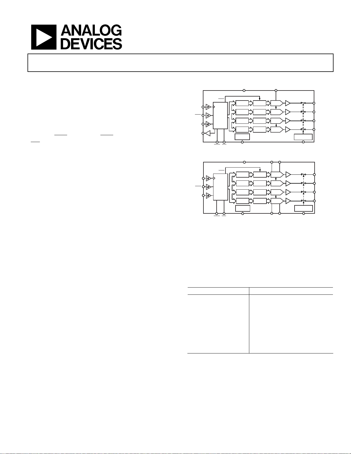
Figure 1. AD5064-1 Functional Equivalent and Pin Compatible with AD5666
V
DD
INPUT
REGISTER
INPUT
REGISTER
INPUT
REGISTER
INPUT
REGISTER
POWER-ON
RESET
POR
REGISTER
REGISTER
REGISTER
REGISTER
SCLK
SYNC
AD5024/
AD5044/
AD5064
LDAC
INTERFACE
LOGIC AND
SHIFT
DIN
REGISTER
LDAC
CLR
Figure 2. AD5024/AD5044/AD5064 with Individual Reference Pins
DAC
DAC
DAC
DAC
DAC
DAC
DAC
DAC
REFIN
BUFFER
DAC A
BUFFER
DAC B
BUFFER
DAC C
BUFFER
DAC D
POWER-DOWN
A
B
REF
REF
BUFFER
DAC A
BUFFER
DAC B
BUFFER
DAC C
BUFFER
DAC D
POWER-DOWN
V
C V
D
REF
REF
LOGIC
GND
LOGIC
GND
V
A
OUT
B
V
OUT
C
V
OUT
D
V
OUT
06803-064
V
A
OUT
V
B
OUT
V
C
OUT
V
D
OUT
06803-001
GENERAL DESCRIPTION
The AD5024/AD5044/AD5064/AD5064-1 are low power, quad
12-/14-/16-bit buffered voltage output nanoDAC® converters
that offer relative accuracy specifications of 1 LSB INL and 1 LSB
DNL with the AD5024/AD5044/AD5064 individual reference
pin and the AD5064-1 common reference pin options. The
AD5024/AD5044/AD5064/AD5064-1 can operate from a single
4.5 V to 5.5 V supply. The AD5024/AD5044/AD5064/AD5064-1
also offer a differential accuracy specification of ±1 LSB. The
parts use a versatile 3-wire, low power Schmitt trigger serial
interface that operates at clock rates up to 50 MHz and is compatible with standard SPI, QSPI™, MICROWIRE™, and DSP interface
standards. Integrated reference buffers and output amplifiers are
also provided on-chip. The AD5024/AD5044/AD5064/AD5064-1
incorporate a power-on reset circuit that ensures the DAC
output powers up to zero scale or midscale and remains there
until a valid write takes place to the device. The AD5024/AD5044/
AD5064/AD5064-1 contain a power-down feature that reduces
the current consumption of the device to typically 400 nA at 5 V
and provides software selectable output loads while in powerdown mode. Total unadjusted error for the parts is <2 mV.
PRODUCT HIGHLIGHTS
1. Quad channel available in 14-/16-lead TSSOP packages.
2. 16-bit accurate, 1 LSB INL.
3. High speed serial interface with clock speeds up to 50 MHz.
4. Reset to known output voltage (zero scale or midscale).
Table 1. Related Devices
Part No. Description
AD5666
AD5025/AD5045/AD5065
AD5062, AD5063
AD5061 16-bit nanoDAC, 4 LSB INL, SOT-23
AD5040/AD5060
Quad,16-bit buffered DAC,
16 LSB INL, TSSOP
Dual, 16-bit buffered DACs,
1 LSB INL, TSSOP
16-bit nanoDAC, 1 LSB INL, SOT-23,
MSOP
14-/16-bit nanoDAC, 1 LSB INL,
SOT-23
Rev. E
Information furnished by Analog Devices is believed to be accurate and reliable. However, no
responsibility is assumed by Anal og Devices for its use, nor for any infringements of patents or ot her
rights of third parties that may result from its use. Specifications subject to change without notice. No
license is granted by implication or otherwise under any patent or patent rights of Analog Devices.
Trademarks and registered trademarks are the property of their respective owners.
One Technology Way, P.O. Box 9106, Norwood, MA 02062-9106, U.S.A.
Tel: 781.329.4700 www.analog.com
Fax: 781.461.3113 ©2008–2011 Analog Devices, Inc. All rights reserved.

AD5024/AD5044/AD5064
TABLE OF CONTENTS
Features.............................................................................................. 1
Applications....................................................................................... 1
Functional Block Diagrams............................................................. 1
General Description ......................................................................... 1
Product Highlights ........................................................................... 1
Revision History ............................................................................... 2
Specifications..................................................................................... 3
AC Characteristics........................................................................ 4
Timing Characteristics ................................................................ 5
Absolute Maximum Ratings............................................................ 7
ESD Caution.................................................................................. 7
Pin Configurations and Function Descriptions ........................... 8
Typical Performance Characteristics ........................................... 10
Terminology .................................................................................... 17
Theory of Operation ...................................................................... 19
Digital-to-Analog Converter .................................................... 19
DAC Architecture....................................................................... 19
Reference Buffer ......................................................................... 19
Output Amplifier........................................................................ 19
Serial Interface............................................................................ 19
Shift Register............................................................................... 19
Modes of Operation................................................................... 21
Power-On Reset.......................................................................... 22
Power-Down Modes .................................................................. 22
Clear Code Register ................................................................... 23
LDAC
Function .......................................................................... 23
Power Supply Bypassing and Grounding................................ 24
Microprocessor Interfacing....................................................... 25
Applications Information.............................................................. 26
Using a Reference as a Power Supply....................................... 26
Bipolar Operation....................................................................... 26
Using the AD5024/AD5044/AD5064/AD5064-1 with a
Galvanically Isolated Interface ................................................. 26
Outline Dimensions....................................................................... 27
Ordering Guide .......................................................................... 28
REVISION HISTORY
5/11—Rev. D to Rev. E
Changes to Table 4............................................................................ 5
Changes to Figure 4 and Figure 5................................................... 6
8/10—Rev. C to Rev. D
Change to Minimum
Update) Parameter, Table 4 ............................................................. 5
5/10—Rev. B to Rev. C
Changes to Power-On Reset Section............................................ 22
6/09—Rev. A to Rev. B
Changes to Figure 1.......................................................................... 1
3/09—Rev. 0 to Rev. A
Added 14-Lead TSSOP ...................................................... Universal
Added Figure 1; Renumbered Sequentially .................................. 1
Changes to Features Section, General Description Section,
Product Highlights Section, Figure 2, and Table 1....................... 1
Changes to Table 2............................................................................ 3
Changes to Timing Characteristics Section and Table 4............. 5
Added Circuit and Timing Diagrams Section and Figure 3....... 5
Added Figure 5.................................................................................. 6
High Time (Single Channel
SYNC
Changes to Figure 4...........................................................................6
Added Figure 6...................................................................................8
Added Table 6; Renumbered Sequentially .....................................8
Changed Input Shift Register to Shift Register Throughout .......8
Changes to Table 7.............................................................................9
Changes to Typical Performance Characteristics Section ........ 10
Changes to Terminology Section ................................................. 17
Changes to Digital-to-Analog Converter Section, Reference
Buffer Section, Output Amplifier Section, Serial Interface
Section, Shift Register Section, and Table 8................................ 19
Changes to Figure 47, Figure 48, and Figure 49 Captions ........ 20
Added Modes of Operation Section, Daisy-Chaining Section,
Table 10, and Table 11.................................................................... 21
Changes to Table 13 and Power-Down Mode Section .............. 22
Changes to Table 16 ....................................................................... 24
Changes to Figure 52 to Figure 55................................................ 25
Changes to Bipolar Operation Section and Figure 56 to
Figure 58 .......................................................................................... 26
Added Figure 59 ............................................................................. 27
Updated Outline Dimensions....................................................... 27
Changes to Ordering Guide.......................................................... 28
8/08—Revision 0: Initial Version
Rev. E | Page 2 of 28

AD5024/AD5044/AD5064
SPECIFICATIONS
VDD = 4.5 V to 5.5 V, RL = 5 kΩ to GND, CL = 200 pF to GND, 2.5 V ≤ V
T
, unless otherwise noted.
MAX
≤ VDD, unless otherwise specified. All specifications T
REFIN
MIN
to
Table 2.
1, 2
A Grade
Parameter
STATIC PERFORMANCE
B Grade1
Min Typ Max Min Typ Max
3
Resolution 16 16 Bits AD5064/AD5064-1
14 Bits AD5044
12 Bits AD5024
Relative Accuracy (INL)4 ±0.5 ±1 ±0.5 ±4 LSB AD5064/AD5064-1; TA = −40°C to
±0.5 ±2 ±0.5 ±4 LSB AD5064/AD5064-1; TA = −40°C to
±0.25 ±1 LSB AD5044
±0.12 ±0.5 LSB AD5024
Differential Nonlinearity (DNL)4
±0.2 ±1 ±0.2 ±1 LSB
Total Unadjusted Error ±2 ±2 mV V
Offset Error
Offset Error Temperature
Coefficient
4, 5
4, 6
Full-Scale Error4
Gain Error4
Gain Temperature Coefficient
DC Crosstalk
4, 6
±0.2 ±1.8 ±0.2 ±1.8 mV
±2 ±2 µV/°C
±0.01 ±0.07 ±0.01 ±0.07 % FSR
±0.005 ±0.05 ±0.005 ±0.05 % FSR
4, 6
±1 ±1 ppm
40 40 µV Due to single-channel, full-scale output
40 40 µV/mA Due to load current change
40 40 µV Due to powering down (per channel)
OUTPUT CHARACTERISTICS6
Output Voltage Range 0 VDD 0 VDD V
Capacitive Load Stability 1 1 nF RL = 5 kΩ, RL =100 kΩ, and RL = ∞
DC Output Impedance
Normal Mode 0.5 0.5 Ω
Power-Down Mode
Output Connected to
100 100 kΩ Output impedance tolerance ± 20 kΩ
100 kΩ Network
Output Connected to
1 1 kΩ Output impedance tolerance ± 400 Ω
1 kΩ Network
Short-Circuit Current 60 60 mA DAC = full scale, output shorted to GND
45 45 mA DAC = zero scale, output shorted to VDD
Power-Up Time7 4.5 4.5 µs
DC PSRR −92 −92 dB
REFERENCE INPUTS
Reference Input Range 2.2 VDD 2.2 VDD V
Reference Current 35 50 35 50 µA Per DAC channel; individual reference
140 160 140 160 µA Single reference option
Reference Input Impedance 120 120 kΩ Individual reference option
32 32 kΩ Single reference option
LOGIC INPUTS
Input Current8 ±1 ±1 µA
Input Low Voltage, V
Input High Voltage, V
Pin Capacitance6
0.8 0.8 V
INL
2.2 2.2 V
INH
4 4 pF
Unit Conditions/Comments
+105°C
+125°C
= 2.5 V, VDD = 5.5 V
REF
All 1s loaded to DAC register, V
V
< VDD
REF
< VDD
REF
FSR/°C
change, R
V
DD
= 5 kΩ to GND or VDD
L
± 10%, DAC = full scale, V
< VDD
REF
option
Rev. E | Page 3 of 28

AD5024/AD5044/AD5064
1, 2
Unit Conditions/Comments
Parameter
B Grade1
A Grade
Min Typ Max Min Typ Max
LOGIC OUTPUTS (SDO)9
Output Low Voltage, VOL 0.4 0.4 V I
Output High Voltage, VOH V
High Impedance Leakage
− 1 VDD − 1 I
DD
±0.002 ±1 ±0.002 ±1 A
= 2 mA
SINK
SOURCE
= 2 mA
Current
High Impedance Output
Capacitance
6
7 7 pF
POWER REQUIREMENTS
VDD 4.5 5.5 4.5 5.5 V DAC active, excludes load current
10
I
VIH = VDD, VIL = GND, Code = midscale
DD
Normal Mode 4 6 4 6 mA
All Power-Down Modes11 0.4 2 0.4 2 µA TA = −40°C to +105°C
30 30 µA TA = −40°C to +125°C
1
Temperature range is −40°C to +125°C, typical at 25°C.
2
A grade offered in AD5064 only.
3
Linearity and total unadjusted error are calculated using a reduced code range—AD5064/AD5064-1: Code 512 to Code 65,024; AD5044: Code 128 to Code 16,256;
AD5024: Code 32 to Code 4064. Output unloaded.
4
See the Terminology section.
5
Offset error calculated using a reduced code range—AD5064/AD5064-1: Code 512 to Code 65,024; AD5044: Code 128 to Code 16,256; AD5024: Code 32 to Code 4064.
Output unloaded
6
Guaranteed by design and characterization; not production tested.
7
Time to exit power-down mode to normal mode; 32nd clock edge to 90% of DAC midscale value, output unloaded.
8
Current flowing into individual digital pins. VDD = 5.5 V; V
9
AD5064-1 only.
10
Interface inactive. All DACs active. DAC outputs unloaded.
11
All four DACs powered down.
= 4.096 V; Code = midscale.
REF
AC CHARACTERISTICS
VDD = 4.5 V to 5.5 V, RL = 5 kΩ to GND, CL = 200 pF to GND, 2.5 V ≤ V
noted.
Table 3.
Parameter
Output Voltage Settling Time 5.8 8 µs
1, 2
Min Typ Max Unit Conditions/Comments3
¼ to ¾ scale and ¾ to ¼ scale settling to ±1 LSB, R
single-channel update
10.7 13 µs
¼ to ¾ scale and ¾ to ¼ scale settling to ±1 LSB, R
update
Slew Rate 1.5 V/µs
Digital-to-Analog Glitch Impulse 3 nV-sec 1 LSB change around major carry
Reference Feedthrough −90 dB V
Digital Feedthrough 0.1 nV-sec
Digital Crosstalk 1.9 nV-sec
Analog Crosstalk 2 nV-sec
DAC-to-DAC Crosstalk 3.5 nV-sec
AC Crosstalk 6 nV-sec
Multiplying Bandwidth 340 kHz V
Total Harmonic Distortion −80 dB V
Output Noise Spectral Density 64 nV/√Hz DAC code = 0x8400, frequency = 1 kHz
60 nV/√Hz DAC code = 0x8400, frequency = 10 kHz
Output Noise 6 V p-p 0.1 Hz to 10 Hz
1
Guaranteed by design and characterization; not production tested.
2
See the Terminology section.
3
Temperature range is −40°C to +125°C, typical at 25°C.
≤ VDD. All specifications T
REFIN
= 3 V ± 0.86 V p-p, frequency = 100 Hz to 100 kHz
REF
= 3 V ± 0.86 V p-p
REF
= 3 V ± 0.2 V p-p, frequency = 10 kHz
REF
MIN
to T
, unless otherwise
MAX
= 5 kΩ,
L
= 5 kΩ, all channel
L
Rev. E | Page 4 of 28
AD5024/AD5044/AD5064
TIMING CHARACTERISTICS
All input signals are specified with tR = tF = 1 ns/V (10% to 90% of VDD) and timed from a voltage level of (VIL + VIH)/2. See Figure 4 and
Figure 5. V
Table 4.
Parameter1 Symbol Min Typ Max Unit
SCLK Cycle Time t1 20 ns
SCLK High Time t2 10 ns
SCLK Low Time t3 10 ns
SYNC to SCLK Falling Edge Setup Time
Data Setup Time t5 5 ns
Data Hold Time t6 5 ns
SCLK Falling Edge to SYNC Rising Edge
Minimum SYNC High Time (Single Channel Update)
Minimum SYNC High Time (All Channel Update)
SYNC Rising Edge to SCLK Fall Ignore
LDAC Pulse Width Low
SCLK Falling Edge to LDAC Rising Edge
CLR Minimum Pulse Width Low
SCLK Falling Edge to LDAC Falling Edge
CLR Pulse Activation Time
SCLK Rising Edge to SDO Valid t
SCLK Falling Edge to SYNC Rising Edge
SYNC Rising Edge to SCLK Rising Edge
SYNC Rising Edge to LDAC/CLR Falling Edge (Single Channel Update)
SYNC Rising Edge to LDAC/CLR Falling Edge (All Channel Update)
Power-up Time4 4.5 µs
1
Maximum SCLK frequency is 50 MHz at VDD = 4.5 V to 5.5 V. Guaranteed by design and characterization; not production tested.
2
Daisy-chain mode only.
3
Measured with the load circuit of Figure 3. t15 determines the maximum SCLK frequency in daisy-chain mode. AD5064-1 only.
4
Time to exit power-down mode to normal mode of AD5024/AD5044/AD5064/AD5064-1, 32nd clock edge to 90% of DAC midscale value, with output unloaded.
Circuit and Timing Diagrams
= 4.5 V to 5.5 V. All specifications T
DD
MIN
to T
, unless otherwise noted.
MAX
t
17 ns
4
t
5 30 ns
7
t
3 µs
8
t
8 µs
8
t
17 ns
9
t
20 ns
10
t
20 ns
11
t
10 ns
12
t
10 ns
13
t
10.6 µs
14
2, 3
15
2
t
5 ns
16
2
t
8 ns
17
2
t
2 µs
18
2
t
8 µs
18
22 ns
2mA I
OL
TO OUTPUT
PIN
50pF
C
L
2mA I
OH
VOH (MIN) + VOL (MAX)
2
06803-002
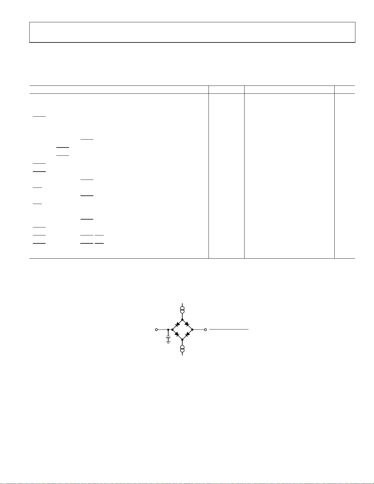
Figure 3. Load Circuit for Digital Output (SDO) Timing Specifications
Rev. E | Page 5 of 28
AD5024/AD5044/AD5064
2
SCLK
t
8
SYNC
DIN
1
LDAC
2
LDAC
CLR
V
OUT
1
ASYNCHRONOUS L DAC UPDATE MO DE.
SYNCHRONOUS L DAC UPDATE MODE .
DB31
t
4
t
6
t
5
t
12
t
14
t
1
t
t
3
2
DB0
t
9
t
7
t
10
t
13
t
11
06803-003
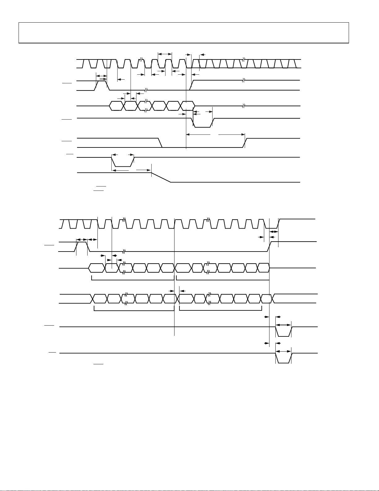
Figure 4. Serial Write Operation
SCLK
SYNC
DIN
t8t
4
t
5
t
6
32 64
t
16
DB0DB31
DB31
DB0
t
17
INPUT WORD F OR DAC N
SDO
UNDEFINED
1
LDAC
CLR
1
IF IN DAIS Y-CHAIN MODE, LDAC MUST BE USED ASYNCHRONOUSLY.
INPUT WO RD FOR DAC N + 1
t
15
DB31
INPUT WO RD FOR DAC N
DB0
t
18
t
18
t
10
t
12
06803-004
Figure 5. Daisy-Chain Timing Diagram
Rev. E | Page 6 of 28
AD5024/AD5044/AD5064
ABSOLUTE MAXIMUM RATINGS
TA = 25°C, unless otherwise noted.
Table 5.
Parameter Rating
VDD to GND −0.3 V to +7 V
Digital Input Voltage to GND −0.3 V to VDD + 0.3 V
V
to GND −0.3 V to VDD + 0.3 V
OUT
V
to GND −0.3 V to VDD + 0.3 V
REF
Operating Temperature Range
Industrial −40°C to +125°C
Storage Temperature Range −65°C to +150°C
Junction Temperature (TJ
TSSOP Package
Power Dissipation (TJ
θJA Thermal Impedance 113°C/W
Reflow Soldering Peak Temperature
Pb-Free 260°C
) 150°C
MAX
− TA)/θJA
MAX
Stresses above those listed under Absolute Maximum Ratings
may cause permanent damage to the device. This is a stress
rating only; functional operation of the device at these or any
other conditions above those indicated in the operational
section of this specification is not implied. Exposure to absolute
maximum rating conditions for extended periods may affect
device reliability.
ESD CAUTION
Rev. E | Page 7 of 28
AD5024/AD5044/AD5064
PIN CONFIGURATIONS AND FUNCTION DESCRIPTIONS
LDAC
SYNC
V
OUT
V
OUT
POR
V
REFIN
V
DD
A
C
1
2
3
AD5064-1
4
TOP VIEW
5
(Not to Scale)
6
7
14
SCLK
DIN
13
12
GND
B
V
11
OUT
D
V
10
OUT
9
CLR
8
SDO
6803-065
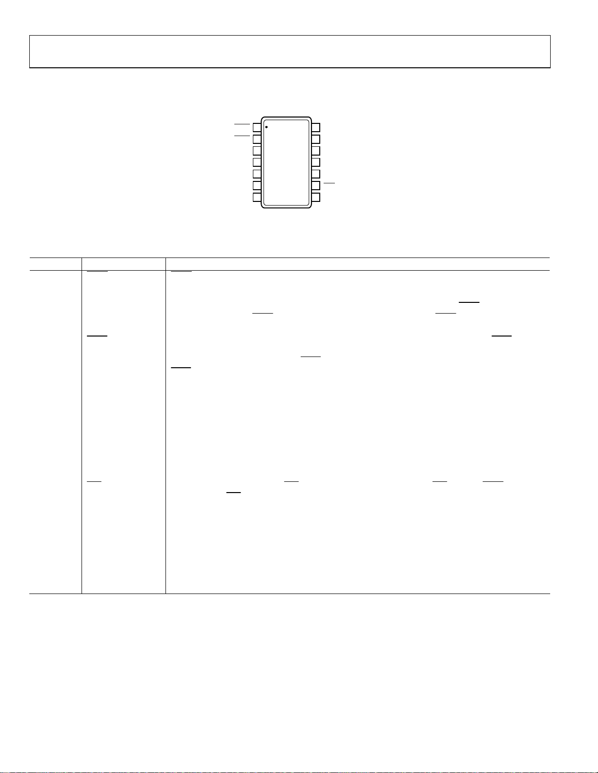
Figure 6. 14-Lead TSSOP (RU-14)
Table 6. Pin Function Descriptions
Pin No. Mnemonic Description
1
LDAC can be operated in two modes, asynchronously and synchronously, as shown in . Pulsing
LDAC
this pin low allows any or all DAC registers to be updated if the input registers have new data. This allows
all DAC outputs to simultaneously update. This pin can also be tied permanently low in standalone mode.
When daisy-chain mode is enabled, this pin cannot be tied permanently low; the
used in asynchronous LDAC
update mode, as shown in , and the Figure 5 LDAC pin must be brought
high after pulsing.
2
Active Low Control Input. This is the frame synchronization signal for the input data. When SYNC goes
SYNC
low, it powers on the SCLK and DIN buffers and enables the shift register. Data is transferred in on the
falling edges of the next 32 clocks. If SYNC is taken high before the 32nd falling edge, the rising edge of
SYNC
acts as an interrupt and the write sequence is ignored by the device.
3 VDD
Power Supply Input. These parts can be operated from 4.5 V to 5.5 V, and the supply should be decoupled
with a 10 µF capacitor in parallel with a 0.1 µF capacitor to GND.
4 V
5 V
6 POR
A Analog Output Voltage from DAC A. The output amplifier has rail-to-rail operation.
OUT
C Analog Output Voltage from DAC C. The output amplifier has rail-to-rail operation.
OUT
Power-On Reset Pin. Tying this pin to GND powers up all four DACs to zero scale. Tying this pin to V
powers up all four DACs to midscale.
7 V
8 SDO
This is a common pin for reference input for DAC A, DAC B, DAC C, and DAC D.
REFIN
Serial Data Output. Can be used to daisy-chain a number of AD5064-1 devices together. The serial data
is transferred on the rising edge of SCLK and is valid on the falling edge of the clock.
9
Asynchronous Clear Input. The CLR input is falling edge sensitive. When CLR is low, all LDAC pulses are
CLR
ignored. When CLR
is activated, the input register and the DAC register are updated with the data
contained in the clear code register—zero, midscale, or full scale. Default setting clears the output to 0 V.
10 V
11 V
D Analog Output Voltage from DAC D. The output amplifier has rail-to-rail operation.
OUT
B Analog Output Voltage from DAC B. The output amplifier has rail-to-rail operation.
OUT
12 GND Ground Reference Point for All Circuitry on the Part.
13 DIN
Serial Data Input. This device has a 32-bit shift register. Data is clocked into the shift register on the
falling edge of the serial clock input.
14 SCLK
Serial Clock Input. Data is clocked into the shift register on the falling edge of the serial clock input. Data
can be transferred at rates of up to 50 MHz.
Figure 4
LDAC
pin should be
DD
Rev. E | Page 8 of 28
AD5024/AD5044/AD5064
V
V
LDAC
SYNC
V
V
REF
V
REF
OUT
OUT
POR
DD
B
A
A
C
1
2
3
AD5024/
AD5044/
4
AD5064
5
TOP VIEW
6
(Not to Scale)
7
8
SCLK
16
15
DIN
14
GND
B
V
13
OUT
D
V
12
OUT
V
D
11
REF
10
CLR
9
C
V
REF
06803-005
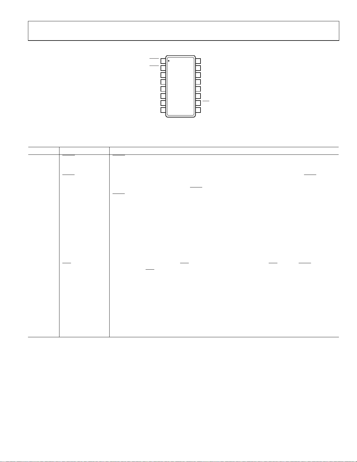
Figure 7. 16-Lead TSSOP (RU-16) Pin Configuration
Table 7. Pin Function Descriptions
Pin No. Mnemonic Description
1
LDAC can be operated in two modes, asynchronously and synchronously, as shown in . Pulsing
LDAC
this pin low allows any or all DAC registers to be updated if the input registers have new data. This allows
all DAC outputs to simultaneously update. This pin can also be tied permanently low in standalone mode.
2
Active Low Control Input. This is the frame synchronization signal for the input data. When SYNC goes
SYNC
low, it powers on the SCLK and DIN buffers and enables the shift register. Data is transferred in on the
falling edges of the next 32 clocks. If SYNC
is taken high before the 32nd falling edge, the rising edge of
SYNC acts as an interrupt and the write sequence is ignored by the device.
3 VDD
Power Supply Input. These parts can be operated from 4.5 V to 5.5 V, and the supply should be decoupled
with a 10 µF capacitor in parallel with a 0.1 µF capacitor to GND.
4 V
5 V
6 V
7 V
8 POR
B DAC B Reference Input. This is the reference voltage input pin for DAC B.
REF
A DAC A Reference Input. This is the reference voltage input pin for DAC A.
REF
A Analog Output Voltage from DAC A. The output amplifier has rail-to-rail operation.
OUT
C Analog Output Voltage from DAC C. The output amplifier has rail-to-rail operation.
OUT
Power-On Reset. Tying this pin to GND powers up the part to 0 V. Tying this pin to V
part to midscale.
9 V
10
C DAC C Reference Input. This is the reference voltage input pin for DAC C.
REF
Asynchronous Clear Input. The CLR input is falling edge sensitive. When CLR is low, all LDAC pulses are
CLR
ignored. When CLR
is activated, the input register and the DAC register are updated with the data
contained in the clear code register—zero, midscale, or full scale. Default setting clears the output to 0 V.
11 V
12 V
13 V
D DAC D Reference Input. This is the reference voltage input pin for DAC D.
REF
D Analog Output Voltage from DAC D. The output amplifier has rail-to-rail operation.
OUT
B Analog Output Voltage from DAC B. The output amplifier has rail-to-rail operation.
OUT
14 GND Ground Reference Point for All Circuitry on the Part.
15 DIN
Serial Data Input. This device has a 32-bit shift register. Data is clocked into the shift register on the
falling edge of the serial clock input.
16 SCLK
Serial Clock Input. Data is clocked into the shift register on the falling edge of the serial clock input. Data
can be transferred at rates of up to 50 MHz.
Figure 4
powers up the
DD
Rev. E | Page 9 of 28
 Loading...