PRELIMINARY TECHNICAL DA TA
2 Pair/1 Pair ETSI Compatible
a
HDSL Analog Front End
Preliminary Technical Data AD5011
FEATURES
Integrated front End for Single Pair or Two Pair HDSL
Systems
Meets ETSI Specifications
Supports 1168 kbps and 2.32 Mbps
Programmable Filtering Supports Adaptive HDSL
Transmit and Receive Signal Path Functions
Receive Hybrid Amplifier, PGA, ADC and Adaptable
Filter
Transmit DAC, Adaptable Filter and Differential
Outputs
Normal Loopback
Serial Interface to Digital Transceivers
Single 3 V Power Supply
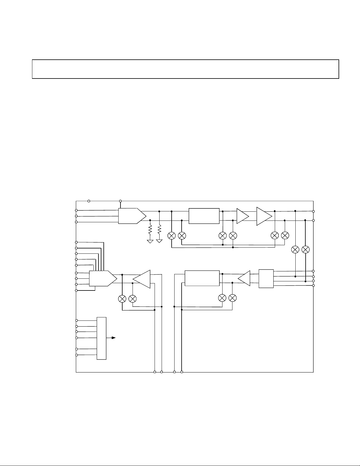
FUNCTIONAL BLOCK DIAGRAM
VDRIVE
TxDATA
TxSYNC
TxCLK
Tx-DECOUP
14-Bit DAC
GENERAL DESCRIPTION
The AD5011 is an analog front end for two pair or single
pair HDSL applications that use 1168 kbps or 2.32 Mbps
data rates. The device integrates all the transmit and receive
functional blocks. A standard serial interface is used to
communicate with the DAC and ADC. The filters in both
the transmit and receive paths are programmable which
allows adaptive HDSL to be performed also. The part is
available in a 48-pin LQFP package and is specified for a
temperature range of -40
6 Pole Adaptive
Be s s el Filt e r
PGA
0 dB
-6 dB
o
C to +85 oC.
Line
Driver
DRV-OUTP
DRV-OUTN
ADCCLK
SCLK
SDO
DR
CAP-T
CAP-B
REF-COM
VREF
CM-LVL
SPICLK
TFS
DT
DR
RESETB
PWRDOW NB
12-Bit ADC
SPI
Control/
Configuration
ADC
Buffer
ADCINN
ADCINP
4 Pole Adaptive
Butterworth Filter
FILOUTP
FILOUTN
-6 dB
-3 dB
0 dB
+3 dB
+6 dB
HYBIN-2B
HybridPGA
HYBIN-2A
HYBIN-1A
HYBIN-1B
REV PrA
Information furnished by Analog Devices is believed to be accurate and
reliable. However, no responsibility is assumed by Analog Devices for its
use, nor for any infringements of patents or other rights of third parties
which may result from its use. No license is granted by implication or
otherwise under any patent or patent rights of Analog Devices.
One Technology Way, P.O. Box 9106, Norwood, MA 02062-9106, U.S.A.
Tel: 781/329-4700 Fax: 781/326-8703
World Wide Web Site: hppt://www.analog.com

PRELIMINARY TECHNICAL DA TA
AD5011–SPECIFICATIONS
(VDD = +3.15 V to +3.45 V; AGND = DGND = 0 V; TA = T
1
noted)
MIN
to T
unless otherwise
MAX
Parameter AD5011B Units Test Conditions/Comments
Min Typ Max
TRANSMIT CHANNEL
Signal to Noise
Total Harmonic Distortion
2
2
68 71 dB F
66 71 dB F
= 73 kHz
OUT
= 73 kHz
OUT
TRANSMIT DAC
Resolution 14 Bits
Clock Frequency 18.688 MH z
Coding 2s Complement
Output Update Rate
3
1168 kHz
Output Voltage 1 Vpp Diff
TRANSMIT FILTER
Cutoff Frequency
4
49 - 120.8 kHz Bottom Range (8 kHz steps)
108 - 265 kHz Mid Range (18 kHz steps)
235 - 580 kHz Top Range (40.5 kHz steps)
Corner Frequency Accuracy
+5 +10 %
Adjacent Corner Step +40 % nom
LINE DRIVER
5
VCM 1.5 V
Common Mode Voltage Error
+100 mV
Output Power 13.5 dB m
Output Voltage 4 Vpp Diff Tx-GAIN = 0
2 Vpp Diff Tx-GAIN = 1
Channel Gain Accuracy +1 dB
RECEIVE CHANNEL
Signal to (Noise + Distortion)
6
66 68 dB FIN = 73 kHz
Total Harmonic Distortion 68 71 d B FIN = 73 kHz
HYBRID INTERFACE
Input Voltage Range 5 Vpp Diff PGA = 0 dB
Common Mode Input Voltage 1.5 V
Input Impedance 10 k W
Input Offset Voltage 80 m V PGA = 0 dB
PROGRAMMABLE GAIN AMPLIFIER
Overall Gain Accuracy
7
For all Gain Settings from -6 dB to +9 dB
+1 dB
Gain Step 3 d B
Gain Step Accuracy +0.25 dB
RECEIVE FILTER
Cutoff Frequency
4
49 - 120.8 kHz Bottom Range (8 kHz steps)
108 - 265 kHz Mid Range (18 kHz steps)
235 - 580 kHz Top Range (40.5 kHz steps)
Accuracy
Adjacent Corner Step
+5 +10 %
+40 % nom
Output Load Capacitance 20 p F
Output Load Resistance T BD W
RECEIVE ADC
Resolution 12 Bits
Coding 2s Complement
Sample Rate 2.32 MHz
LOGIC INPUTS
Input Logic High, V
Input Logic Low, V
I
, Input Current +10 m AV
IN
INH
INL
8
23 V
0 0.2 V
= 0 V to DVDD
IN
CIN, Input Capacitance 10 pF
–2–
REV PrA

PRELIMINARY TECHNICAL DA TA
AD5011
Parameter AD7346B Units Test Conditions/Comments
Min Typ Max
LOGIC OUTPUTS
Output Logic High, V
Output Logic Low, V
OH
OL
9
VDD - 0.3 V I
0.3 V I
OUT
OUT
= 200 mA
= 200 mA
POWER SUPPLIES
AVDD, DVDD 3.15 3.3 3.45 V
IDD
Normal Mode (excluding Driver) 32 m A
Line Driver 75 mA 33 W Differential Load
1
Operating temperature range is as follows: B Version: –40°C to +85°C.
2
The complete transmit path spectrum and pulse shape comply with ETSI requirements. SNR and THD are measured within a 547 kHz bandwidth. Noise and Spurious
tones beyong 540 kHz are therefore excluded.
3
The transmit DAC maximum update rate is half the maximum output data rate i.e. 1168 kHz. The maximum transmit clock is 16 x 1168 = 18.688 MHz.
4
There are three ranges (bottom range, mid range, top range), each range being divided into eight steps. The transmit filter corner frequency can be set independently from
the receive filter corner frequency. the filter tuning circuit requires a continuous 16.384 MHz clock applied to the Fclk pin.
5
Transformer turns ratio = 1:2:3 at 50 kHz when loaded by ETSI (RTR/TM3036) HDSL test loops.
6
With 547 kHz filter snd 0 dB PGA gain selected.
7
The PGA gain is set by setting the PGA-GC bits in the control register.
8
The input switching threshold voltage is approximately 1.2 V to allow interfacing to 2.5 V and 3.3 V logic.
9
The output level is determined by the voltage on the logic supply pin V
Specifications subject to change without notice.
DRIVE
.
REV PrA
–3–
 Loading...