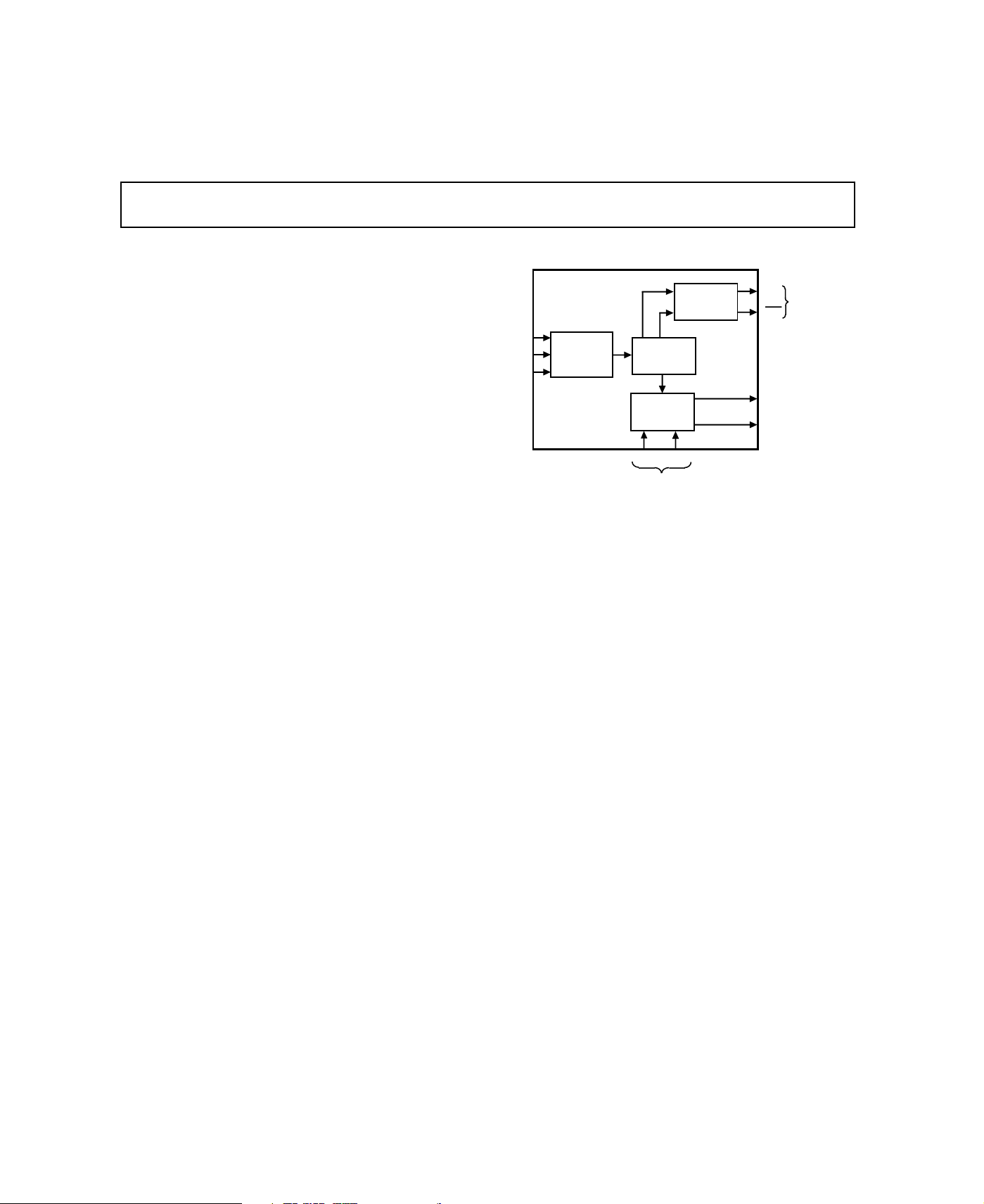
Programmable
FREQUENCY
SELECT
SINE WAVE
GENERATOR
PHASE
DETECT
LOGIC
SIN COS
FROM
TRANSDUCER
FBIAS
SEL1
SEL2
AD2S99
EXC
SYNREF
SYNCHRONOUS
REFERENCE
LOS
TO
TRANSDUCER
PUSH/
PULL
O/P STAGE
EXC
a
FEATURES
Programmable Sinusoidal Oscillator
Synthesized Synchronous Reference Output
Programmable Output Frequency Range: 2 kHz–20 kHz
“Loss-of-Signal” Indicator
20-Pin PLCC Package
Low Cost
APPLICATIONS
Excitation Source for:
Resolvers
Synchros
LVDTs
RVDTs
Pressure Transducers
Load Cells
AC Bridges
Oscillator
AD2S99
FUNCTIONAL BLOCK DIAGRAM
GENERAL DESCRIPTION
The AD2S99 programmable sinusoidal oscillator provides sine
wave excitation for resolvers and a wide variety of ac transducers. The AD2S99 also provides a synchronous reference output
signal (3 V p-p square wave) that is phase locked to its SIN and
COS inputs. In an application, the SIN and COS inputs are
connected to the transducer’s secondary windings.
The synchronous reference output compensates for temperature
and cabling dependent phase shifts and eliminates the need for
external preset phase compensation circuits. The synchronous
reference output can be used as a zero crossing reference for
resolver-to-digital converters such as Analog Devices’ AD2S80A,
AD2S82A, AD2S83 and AD2S90.
The AD2S99 is packaged in a 20-pin PLCC and operates over
–40°C to +85°C.
REV. B
Information furnished by Analog Devices is believed to be accurate and
reliable. However, no responsibility is assumed by Analog Devices for its
use, nor for any infringements of patents or other rights of third parties
which may result from its use. No license is granted by implication or
otherwise under any patent or patent rights of Analog Devices.
PRODUCT HIGHLIGHTS
Dynamic Phase Compensation
The AD2S99 dynamically compensates for any phase variation
in a transducer by phase locking its synchronous reference output to the transducer’s secondary windings.
Programmable Excitation Frequency
The excitation frequency is easily programmed to 2 kHz, 5 kHz,
10 kHz, or 20 kHz by using the frequency select pins. Intermediate frequencies are available by adding an external resistor.
Signal Loss Detection
The AD2S99 has the ability to detect if both the transducer secondary winding connections become disconnected from its SIN
and COS inputs. The “LOS” output pin pulls high when a signal loss is detected.
Integration
The AD2S99 integrates the transducer excitation, synchronous
reference, and loss of signal detection functions into a small,
cost effective package.
© Analog Devices, Inc., 1995
One Technology Way, P.O. Box 9106, Norwood. MA 02062-9106, U.S.A.
Tel: 617/329-4700 Fax: 617/326-8703

AD2S99–SPECIFICATIONS
(VS = 64.75 V to 65.25 V @ –408C to +858C unless otherwise noted)
Parameter Min Typ Max Units Test Conditions
FREQUENCY OUTPUT RANGE SEL1 SEL2
2 kHz 2000 Hz V
5 kHz 5000 Hz V
SS
SS
10 kHz 10000 Hz GND V
V
SS
GND
SS
20 kHz 20000 Hz GND GND
ACCURACY
Frequency ±10 % AP Grade @ +25°C
±20 % AP Grade –40°C to +85°C
±5 % BP Grade @ +25°C
±10 % BP Grade –40°C to +85°C
Amplitude ±3 ±10 % AP Grade @ +25°C
±20 % AP Grade –40°C to +85°C
±3 ±5 % BP Grade @ +25°C
±10 % BP Grade –40°C to +85°C
Power Supply Rejection Ratio 0.002 V p-p/V Output Variation as Function of
Change in Power Supply Voltage
ANALOG OUTPUTS
Amplitude
EXC 2 V rms EXC to GND, EXC to GND
EXC,
SYNREF ±3 V p-p Square Wave
SYNREF OFFSET ±200 mV
Current Drive Capability
EXC,
EXC V
= ±5 V 8 mA rms R
S
= 500 Ω EXC to EXC
LOAD
= 1000 pF
C
LOAD
Capacitive Drive 1000 pF
Total Harmonic Distortion
EXC, EXC –25 dB
ANALOG INPUTS SIN, COS
Amplitude 1.8 2.0 2.2 V rms
Phase Lock Range –45 +45 Degrees
Additional Phase Delay
±10 Degrees AP Grade
±10 Degrees BP Grade
FREQUENCY SELECT INPUTS
SEL1, SEL2
1
V
SS
AGND V dc
LOS OUTPUT
Output Low Voltage 0.7 V dc I
Output High Voltage V
DD
V dc 50 kΩ Pull Up to V
SIN, COS LOS Threshold 0.5 0.6 0.8 V rms
POWER SUPPLIES
V
DD
V
SS
Quiescent Current IDD, I
SS
+4.75 +5.25 V dc
–4.75 –5.25 V dc
±8 ±15 mA No Load
TEMPERATURE RANGE
Operating –40 +85 °C
Storage –65 +150 °C
NOTES
1
Frequency select pins SEL1 and SEL2 must be connected to appropriate voltage levels before power is applied.
Specifications subject to change without notice.
= 400 µA
OL
Drain Output)
(Open
DD
–2–
REV. B

AD2S99
WARNING!
ESD SENSITIVE DEVICE
ABSOLUTE MAXIMUM RATINGS*
VDD . . . . . . . . . . . . . . . . . . . . . . . . . . . . . . . . . . . . . . . . . +7 V
. . . . . . . . . . . . . . . . . . . . . . . . . . . . . . . . . . . . . . . . . . –7 V
V
SS
Operating Temperature . . . . . . . . . . . . . . . . . .–40°C to +85°C
Storage Temperature . . . . . . . . . . . . . . . . . . .–65°C to +150°C
Analog Input Voltages (SIN and COS) . . . . . . . . . V
. . . . . . . . . . . . . . . . . . . . . . . . . . . . . . . . . . . .to V
Frequency Select (SEL1, SEL2) . . . . . . . . . . . . . . V
– 0.3 V
SS
+ 0.3 V
DD
– 0.4 V
SS
. . . . . . . . . . . . . . . . . . . . . . . . . . . . . . . . . to AGND + 0.4 V
*Stresses above those listed under “Absolute Maximum Ratings” may cause
permanent damage to the device. This is a stress rating only and functional
operation of the device at these or any other conditions above those indicated in the
operational section of this specification is not implied. Exposure to absolute
maximum rating conditions for extended periods may affect device reliability.
RECOMMENDED OPERATING CONDITIONS
Power Supply Voltage (VDD to V
) . . . . . . ±4.75 V to ±5.25 V
SS
Analog Input Voltage (SIN and COS) . . . . . . . . 2 V rms ±10%
Frequency Select (SEL1 and SEL2) . . . . . . . . . V
to AGND
SS
Operating Temperature Range . . . . . . . . . . . . .–40°C to +85°C
ORDERING GUIDE
Model Temperature Range Package Option*
AD2S99AP –40°C to +85°C P-20A
AD2S99BP –40°C to +85°C P-20A
*P = PLCC.
PIN DESIGNATIONS
Pin
No. Mnemonic Description
1 SEL2 Frequency Select 2
2 SEL1 Frequency Select 1
3 FBIAS External Frequency Adjust Pin
5 SIN Resolver Output SIN
1
6
DGND Digital Ground
7 COS Resolver Output COS
10 SYNREF Synthesized Reference Output
11 LOS Indicates When Both the SIN and
COS Are Below the Threshold.
12 V
1
16
DD
AGND Analog Ground
Positive Power Supply
17 EXC Resolver Reference One
18
2
19
2
20
NOTES
1
Pins 6 and 16 must be connected together.
2
Pins 19 and 20 must be connected together.
3
Resolver Reference two (EXC) is 180° phase advanced with respect to Resolver
Reference one (EXC).
EXC Resolver Reference Two
V
SS
V
SS
Negative Power Supply
Negative Power Supply
3
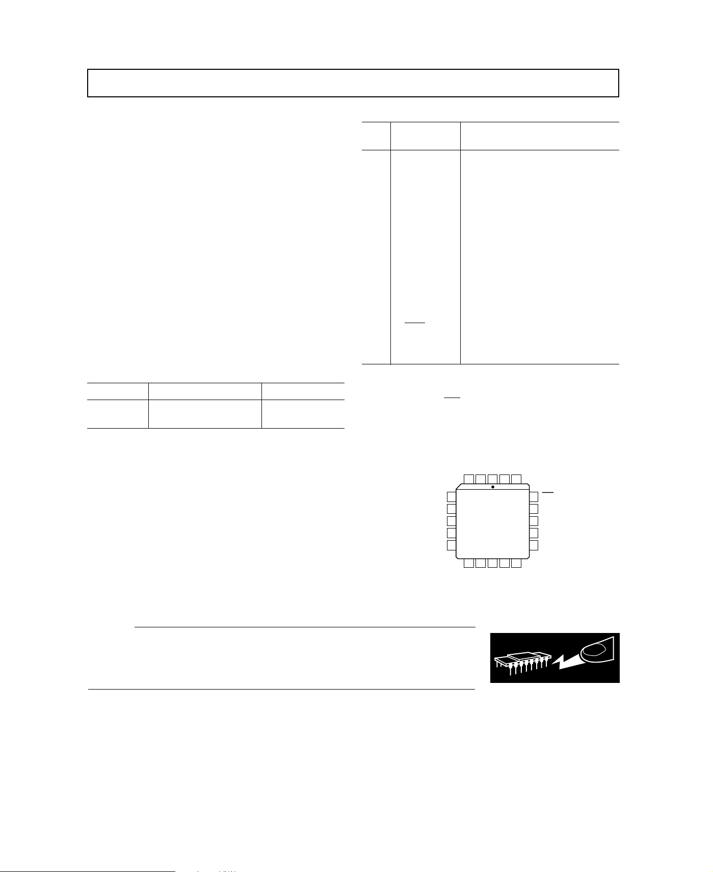
PIN CONFIGURATION
FBIAS
NC
4
SIN
5
DGND
COS
NC
AD2S99
6
TOP VIEW
(Not to Scale)
7
8
NC
NC = NO CONNECT
CAUTION
ESD (electrostatic discharge) sensitive device. Electrostatic charges as high as 4000 V readily
accumulate on the human body and test equipment and can discharge without detection.
Although the AD2S99 features proprietary ESD protection circuitry, permanent damage may
occur on devices subjected to high energy electrostatic discharges. Therefore, proper ESD
precautions are recommended to avoid performance degradation or loss of functionality.
SEL2
SEL1
LOS
SYNREF
SS
SS
V
V
19312 20
EXC
18
EXC
17
AGND
16
NC
15
NC
14
12 1391110
DD
NC
V
REV. B
–3–
 Loading...