

Analog Devices AD2S83 e Datasheet
Variable Resolution,
A3
RIPPLE
CLOCK
R4
VCO
I/P
TRACKING
RATE
SELECTION
R6
VELOCITY
SIGNAL
INTEGRATOR
I/P
BANDWIDTH
SELECTION
R3
C3
REFERENCE
I/P
HF FILTER
R2
C2
C1
R1
DEMOD
O/P
INTEGRATOR
O/P
DIRECTION
BUSY
DIG
GND
16
DATA BITS
SC1
SC2
DATA
LOAD
BYTE
SELECT
5V
+12V
–12V
GND
COS
SIG
GND
SIN
AC ERROR O/P
VCO
O/P
C7
AD2S83
R7
3K3
C6
390pF
R8
–12V
+12V
OFFSET ADJUST
R9
R5
C4
C5
R – 2R DAC
PHASE
SENSITIVE
DETECTOR
VCO + DATA
TRANSFER
LOGIC
16-BIT UP/DOWN COUNTER
SEGMENT
SWITCHING
OUTPUT DATA LATCH
A2
A1
ENABLE INHIBIT
a
FEATURES
Tracking R/D Converter
High Accuracy Velocity Output
High Max Tracking Rate 1040 RPS (10 Bits)
44-Lead PLCC Package
10-, 12-, 14-, or 16-Bit Resolution Set by User
Ratiometric Conversion
Stabilized Velocity Reference
Dynamic Performance Set by User
Industrial Temperature Range
APPLICATIONS
DC and AC Servo Motor Control
Process Control
Numerical Control of Machine Tools
Robotics
Axis Control
Resolver-to-Digital Converter
AD2S83
FUNCTIONAL BLOCK DIAGRAM
GENERAL DESCRIPTION
The AD2S83 is a monolithic 10-, 12-, 14-, or 16-bit tracking
resolver-to-digital converter.
The converter allows users to select their own resolution and dynamic
performance with external components. The converter allows users to
select the resolution to be 10, 12, 14, or 16 bits and to track
resolver signals rotating at up to 1040 revs per second (62,400 rpm)
when set to 10-bit resolution.
The AD2S83 converts resolver format input signals into a parallel natural binary digital word using a ratiometric tracking conversion method. This ensures high noise immunity and tolerance
of long leads allowing the converter to be located remote from
the resolver.
The position output from the converter is presented via 3-state
output pins which can be configured for operations with 8- or
16-bit bus. BYTE SELECT, ENABLE and INHIBIT pins
ensure easy data transfer to 8- and 16-bit data bus, and outputs
are provided to allow for cycle or pitch counting in external
counters.
A precise analog signal proportional to velocity is also available
and will replace a tachogenerator.
The AD2S83 operates over reference frequencies in the range
0 Hz to 20,000 Hz.
REV. E
Information furnished by Analog Devices is believed to be accurate and
reliable. However, no responsibility is assumed by Analog Devices for its
use, nor for any infringements of patents or other rights of third parties
which may result from its use. No license is granted by implication or
otherwise under any patent or patent rights of Analog Devices.
PRODUCT HIGHLIGHTS
High Accuracy Velocity Output. A precision analog velocity
signal with a typical linearity of ±0.1% and reversion error less
than ±0.3% is generated by the AD2S83. The provision of this
signal removes the need for mechanical tachogenerators used in
servo systems to provide loop stabilization and speed control.
Resolution Set by User. Two control pins are used to select
the resolution of the AD2S83 to be 10, 12, 14 or 16 bits allowing optimum resolution for each application.
Ratiometric Tracking Conversion. This technique provides
continuous output position data without conversion delay. It
also provides noise immunity and tolerance of harmonic distortion on the reference and input signals.
Dynamic Performance Set by the User. By selecting external
resistor and capacitor values the user can determine bandwidth, maximum tracking rate and velocity scaling of the
converter to match the system requirements. The component
values are easy to select using the free component selection
software design aid.
MODELS AVAILABLE
Information on the models available is given in the Ordering
Guide.
One Technology Way, P.O. Box 9106, Norwood, MA 02062-9106, U.S.A.
Tel: 781/329-4700 World Wide Web Site: http://www.analog.com
Fax: 781/326-8703 © Analog Devices, Inc., 2000

AD2S83–SPECIFICATIONS
(VS = 12 V dc 5%; VL = 5 V dc 10%; TA = –40C to +85C)
Parameter Conditions Min Typ Max Unit
SIGNAL INPUTS (SIN, COS)
Frequency
1
0 20,000 Hz
Voltage Level 1.8 2.0 2.2 V rms
Input Bias Current 60 150 nA
Input Impedance 1.0 MΩ
REFERENCE INPUT (REF)
Frequency 0 20,000 Hz
Voltage Level 1.0 8.0 V pk
Input Bias Current 60 150 nA
Input Impedance 1.0 MΩ
PERFORMANCE
Repeatability 1 LSB
Allowable Phase Shift (Signals to Reference) –10 +10 Degree
Max Tracking Rate 10 Bits 1040 rps
12 Bits 260 rps
14 Bits 65 rps
16 Bits 16.25 rps
Bandwidth User Selectable
ACCURACY
Angular Accuracy A, I
8 +1 LSB arc min
Monotonicity Guaranteed Monotonic
Missing Codes (16-Bit Resolution) A, I 4 Codes
VELOCITY SIGNAL
LINEARITY
2, 3, 4
AD2S83AP
0 kHz–500 kHz –40°C to +85°C ±0.15
0.5 MHz–1 MHz –40°C to +85°C ±0.25
0.25 % FSR
1.0 % FSR
AD2S83IP
0 kHz–500 kHz –40°C to +85°C ±0.25
0.5 MHz–1 MHz –40°C to +85°C ±0.25
0.5 % FSR
1.0 % FSR
Reversion Error
AD2S83AP –40°C to +85°C ±0.5
AD2S83IP –40°C to +85°C ±1.0
DC Zero Offset
5
±3mV
1.0 % O/P
1.5 % O/P
Gain Scaling Accuracy ±1.5 3 % FSR
Output Voltage 1 mA Load ±8V
Dynamic Ripple Mean Value 1.0 % rms O/P
INPUT/OUTPUT PROTECTION
Analog Inputs Overvoltage Protection ±8V
Analog Outputs Short Circuit O/P Protection ±5.6 ±8 ±10.4 mA
DIGITAL POSITION
Resolution 10, 12, 14, and 16 Bits
Output Format Bidirectional Natural Binary
Load 3 LSTTL
INHIBIT
6
Sense Logic LO to INHIBIT
Time to Stable Data 240 390 490 ns
ENABLE
6
Logic LO Enables Position Output
Logic HI Outputs in High
ENABLE6/Disable Time Impedance State 35 110 ns
BYTE SELECT
6
Sense
Logic HI MS Byte DB1–DB8
Logic LO LS Byte DB1–DB8
Time to Data Available 60 140 ns
SHORT CYCLE INPUTS Internally Pulled High via
100 kΩ to +V
S
SC1 SC2
0 0 10-Bit Resolution
0 1 12-Bit Resolution
1 0 14-Bit Resolution
1 1 16-Bit Resolution
–2–
REV. E

AD2S83
Parameter Conditions Min Typ Max Unit
COMPLEMENT Internally Pulled High via 100 kΩ
DATA LOAD
Sense Internally Pulled High via 100 kΩ 150 300 ns
6, 7
BUSY
Sense Logic HI When Position O/P Changing
Width 150 350 ns
Load Use Additional Pull-Up (See Figure 2) 1 LSTTL
DIRECTION
6
Sense Logic HI Counting Up
Max Load 3 LSTTL
RIPPLE CLOCK
6
Sense Logic HI
Width Dependent on Input Velocity 300 ns
Reset Before Next Busy
Load 3 LSTTL
DIGITAL INPUTS
Input High Voltage, V
Input Low Voltage, V
IH
IL
DIGITAL INPUTS
Input High Current, I
Input Low Current, I
IH
IL
DIGITAL INPUTS
Low Voltage, V
Low Current, I
IL
IL
DIGITAL OUTPUTS
High Voltage, V
Low Voltage, V
NOTES
1
Angular accuracy is not guaranteed <50 Hz reference frequency.
2
Linearity derates from 500 kHz–1000 kHz @ 0.0017%/kHz.
3
Refer to Definition of Linearity, “The AD2S83 as a Silicon Tachogenerator.”
4
Worst case reversion error at temperature extremes.
5
Velocity output offset dependent on value for R6.
6
Refer to timing diagram.
7
Busy pulse guaranteed up to a VCO rate of 900 kHz.
All min and max specifications are guaranteed. Specifications in boldface are tested on all production units at final electrical test.
Specifications subject to change without notice.
OH
OL
. Logic LO to Activate;
to +V
S
No Connect for Normal Operation
. Logic LO Allows
to +V
S
Data to be Loaded into the
Counters from the Data Lines
Logic LO Counting Down
All 1s to All 0s
All 0s to All 1s
INHIBIT, ENABLE 2.0 V
DB1–DB16, Byte Select
= ±11.4 V, VL = 5.0 V
±V
S
INHIBIT, ENABLE 0.8 V
DB1–DB16, Byte Select
±VS = ±12.6 V, VL = 5.0 V
INHIBIT, ENABLE
100 µA
DB1–DB16
±V
= ±12.6 V, VL = 5.5 V
S
INHIBIT, ENABLE
100 µA
DB1–DB16, Byte Select
±VS = ±12.6 V, VL = 5.5 V
ENABLE = HI 1.0 V
SC1, SC2, DATA LOAD
±V
= ±12.0 V, VL = 5.0 V
S
ENABLE = HI –400 µA
SC1, SC2, DATA LOAD
±VS = ±12.0 V, VL = 5.0 V
DB1–DB16 2.4 V
RIPPLE CLK, DIR
= ±12.0 V, VL = 4.5 V
±V
S
= 100 µA
I
OH
DB1–DB16 0.4 V
RIPPLE CLK, DIR
±V
= ±12.0 V, VL = 5.5 V
S
IOL = 1.2 mA
REV. E
–3–

AD2S83–SPECIFICATIONS
(VS = 12 V dc 5%; VL = 5 V dc 10%; TA = –40C to +85C)
Parameter Conditions Min Typ Max Unit
THREE-STATE LEAKAGE DB1–DB16 Only
Current I
L
±VS = ±12.0 V, VL = 5.5 V
V
= 0 V
OL
= ±12.0 V, VL = 5.5 V
±V
S
V
= 5.0 V
OH
20 µA
20 µA
RATIO MULTIPLIER
AC Error Output Scaling 10 Bit 177.6 mV/Bit
12 Bit 44.4 mV/Bit
14 Bit 11.1 mV/Bit
16 Bit 2.775 mV/Bit
PHASE SENSITIVE DETECTOR
Output Offset Voltage 12 mV
Gain
In Phase w.r.t. REF –0.882 –0.9 –0.918 V rms/V dc
In Quadrature w.r.t. REF ±0.02 V rms/V dc
Input Bias Current 60 150 nA
Input Impedance 1.0 MΩ
Input Voltage ±8V
INTEGRATOR
Open-Loop Gain At 10 kHz 57 60 63 dB
Dead Zone Current (Hysteresis) 90 100 110 nA/LSB
Input Offset Voltage 15 mV
Input Bias Current 60 150 nA
Output Voltage Range 8 V
VCO
Maximum Rate 1.1 MHz
VCO Rate +ve DIR 8.25 8.50 8.75 kHz/µA
–ve DIR 8.25 8.50 8.75 kHz/µA
VCO Power Supply Sensitivity
Rate +V
–V
S
S
+0.5 %/V
–0.5 %/V
Input Offset Voltage 3mV
Input Bias Current 12 50 nA
Input Bias Current Tempco +0.22 nA/°C
Linearity of Absolute Rate
AD2S83AP
0 kHz–500 kHz ±0.15 0.25 % FSR
0.5 MHz–1 MHz ±0.25 1.0 % FSR
AD2S83IP
0 kHz–500 kHz ±0.25 0.5 % FSR
0.5 MHz–1 MHz ±0.25 1.0 % FSR
Reversion Error
AD2S83AP ±0.5 1.0 % Output
AD2S83IP ±1.0 1.5 % Output
POWER SUPPLIES
Voltage Levels
+V
–V
+V
S
S
L
+11.4 +12.6 V
–11.4 –12.6 V
+4.5 +5 +V
S
V
Current
±I
S
±I
S
±I
L
All min and max specifications are guaranteed. Specifications in boldface are tested on all production units at final electrical test.
Specifications subject to change without notice.
±VS @ ±12 V ±12 23 mA
±VS @ ±12.6 V ±19 30 mA
+VL @ ±5.0 V ±0.5 1.5 mA
ORDERING GUIDE
Temperature Package Package
Model Range Accuracy Description Option
AD2S83AP –40°C to +85°C 8 arc min Plastic Leaded Chip Carrier P-44A
AD2S83IP –40°C to +85°C 8 arc min Plastic Leaded Chip Carrier P-44A
–4–
REV. E
AD2S83
WARNING!
ESD SENSITIVE DEVICE
ABSOLUTE MAXIMUM RATINGS1
2
+V
. . . . . . . . . . . . . . . . . . . . . . . . . . . . . . . . . . . . . +13 V dc
S
2
. . . . . . . . . . . . . . . . . . . . . . . . . . . . . . . . . . . . . –13 V dc
–V
S
+V
. . . . . . . . . . . . . . . . . . . . . . . . . . . . . . . . . . . . . . . . . . +V
L
Reference . . . . . . . . . . . . . . . . . . . . . . . . . . . . . . . +13 V to –V
SIN . . . . . . . . . . . . . . . . . . . . . . . . . . . . . . . . . . . +13 V to –V
COS . . . . . . . . . . . . . . . . . . . . . . . . . . . . . . . . . . +13 V to –V
(with respect to GND)
S
S
S
S
Any Logical Input . . . . . . . . . . . . . . . . . . –0.4 V dc to +VL dc
Demodulator Input . . . . . . . . . . . . . . . . . . . . . . . +13 V to –V
Integrator Input . . . . . . . . . . . . . . . . . . . . . . . . . . +13 V to –V
VCO Input . . . . . . . . . . . . . . . . . . . . . . . . . . . . . +13 V to –V
S
S
S
Power Dissipation . . . . . . . . . . . . . . . . . . . . . . . . . . . 800 mW
Operating Temperature
Industrial (AP, IP) . . . . . . . . . . . . . . . . . . . –40°C to +85°C
Storage Temperature . . . . . . . . . . . . . . . . . . –65°C to +150°C
Lead Temperature (Soldering, 10 sec) . . . . . . . . . . . . . 300°C
CAUTION
1
Absolute Maximum Ratings are those values beyond which damage to the device
may occur.
2
Correct polarity voltages must be maintained on the +VS and –VS pins.
RECOMMENDED OPERATING CONDITIONS
Power Supply Voltage (+VS, –VS) . . . . . . . . . . ± 12 V dc ± 5%
Power Supply Voltage V
. . . . . . . . . . . . . . . . . +5 V dc ± 10%
L
Analog Input Voltage (SIN and COS) . . . . . . . 2 V rms ± 10%
Analog Input Voltage (REF) . . . . . . . . . . . . . . 1 V to 8 V peak
Signal and Reference Harmonic Distortion . . . . . . 10% (max)
Phase Shift Between Signal and Reference . . . ±10 Degrees (max)
Ambient Operating Temperature Range
Industrial (AP, IP) . . . . . . . . . . . . . . . . . . . –40°C to +85°C
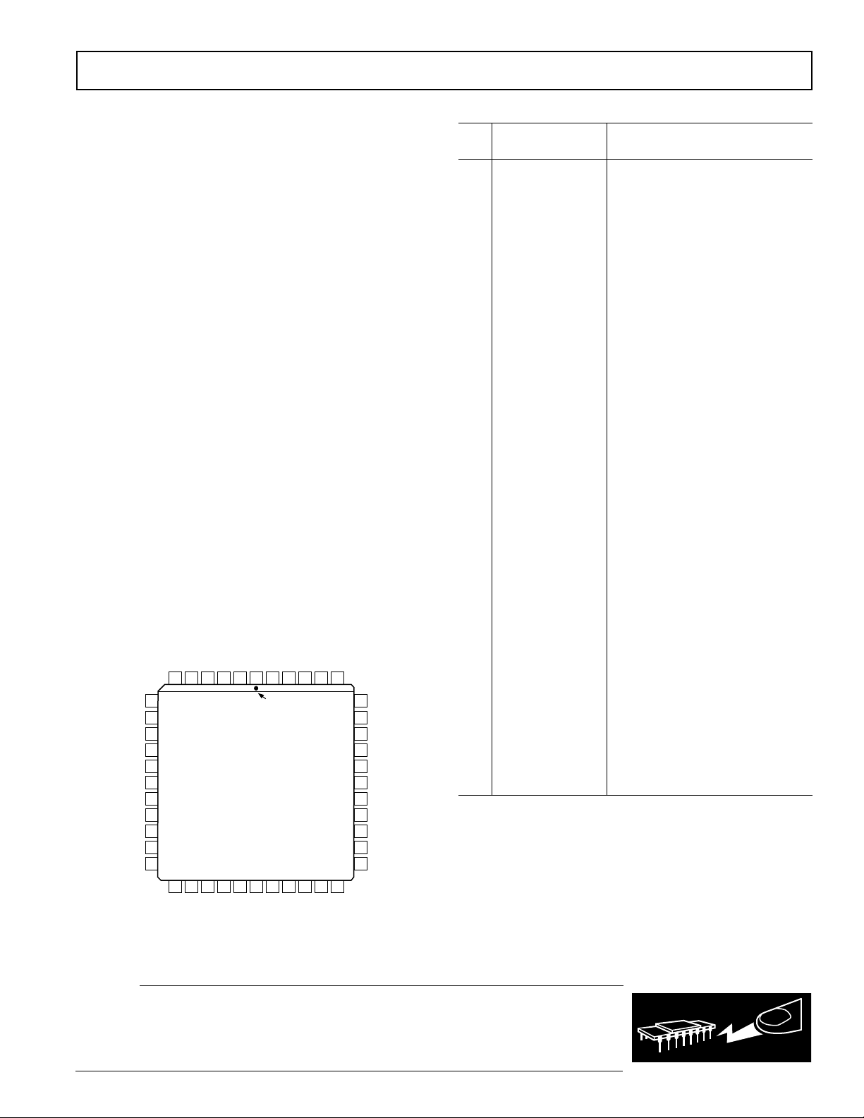
PIN CONFIGURATION
VCO I/P
VCO O/P
INTEGRATOR O/P
39
–V
38
RIPPLE CLOCK
37
DIRECTION
36
BUSY
35
COMP
34
DATA LOAD
33
SC1
SC2
32
DIGITAL GND
31
30
INHIBIT
NC
29
L
+V
ENABLE
BYTE SELECT
S
7
SIN I/P
8
+V
S
9
NC
DB2
DB3
DB4
DB5
DB6
DB7
DB8
10
11
12
13
14
15
16
17
(MSB) DB1
NC = NO CONNECT
ANALOG GND
AC ERROR O/P
DEMOD O/P
SIGNAL GND
5642414043
181920 21 2 2 23 24 252627 28
DB9
DB10
COS I/P
4
DB11
REF I/P
21443
AD2S83
TOP VIEW
(Not to Scale)
DB13
DB12
DEMOD I/P
PIN 1
IDENTIFIER
DB15
DB14
INTEGRATOR I/P
(LSB) DB16
PIN FUNCTION DESCRIPTIONS
P
in
Nos. Mnemonic Description
1 DEMOD O/P Demodulator Output
2 REFERENCE I/P Reference Signal Input
3 AC ERROR O/P Ratio Multiplier Output
4 COS Cosine Input
5 ANALOG GND Power Ground
6 SIGNAL GND Resolver Signal Ground
7 SIN Sine Input
8+V
S
Positive Power Supply
10–25 DB1–DB16 Parallel Output Data
26 +V
L
Logic Power Supply
27 ENABLE Logic HI—Output Data Pins in
High Impedance State
Logic LO—Presents Active Data
to the Output Pins
28 BYTE SELECT Logic HI—Most Significant Byte to
DB1–DB8
Logic LO—Least Significant Byte
to DB1–DB8
30 INHIBIT Logic LO Inhibits Data Transfer
to Output Latches
31 DIGITAL GND Digital Ground
32, 33 SC2–SC1 Select Converter Resolution
34 DATA LOAD Logic LO DB1–DB16 Inputs
Logic HI DB1–DB16 Outputs
35 COMPLEMENT Active Logic LO
36 BUSY Converter Busy, Data not Valid
While Busy HI
37 DIRECTION Logic State Defines Direction of
Input Signal Rotation
38 RIPPLE CLOCK Positive Pulse When Converter Output
Changes from 1s to All 0s or Vice Versa
39 –V
S
Negative Power Supply
40 VCO I/P VCO Input
41 VCO O/P VCO Output
42 INTEGRATOR O/P Integrator Output
43 INTEGRATOR I/P Integrator Input
44 DEMOD I/P Demodulator Input
CAUTION
ESD (electrostatic discharge) sensitive device. Electrostatic charges as high as 4000 V readily
accumulate on the human body and test equipment and can discharge without detection. Although
the AD2S83 feature proprietary ESD protection circuitry, permanent damage may occur on devices
subjected to high-energy electrostatic discharges. Therefore, proper ESD precautions are
recommended to avoid performance degradation or loss of functionality.
REV. E
–5–
AD2S83
Bit Weight Table
Binary Resolution Degrees Minutes Seconds
Bits (N) (NN) /Bit /Bit /Bit
0 1 360.0 21600.0 1296000.0
1 2 180.0 10800.0 648000.0
2 4 90.0 5400.0 324000.0
3 8 45.0 2700.0 162000.0
4 16 22.5 1350.0 81000.0
5 32 11.25 675.0 40500.0
6 64 5.625 337.5 20250.0
7 128 2.8125 168.75 10125.0
8 256 1.40625 84.375 5062.5
9 512 0.703125 42.1875 2531.25
10 1024 0.3515625 21.09375 1265.625
11 2048 0.1757813 10.546875 632.8125
12 4096 0.0878906 5.273438 316.40625
13 8192 0.0439453 2.636719 158.20313
14 16384 0.0219727 1.318359 79.10156
15 32768 0.0109836 0.659180 39.55078
16 65536 0.0054932 0.329590 19.77539
17 131072 0.0027466 0.164795 9.88770
18 262144 0.0013733 0.082397 4.94385
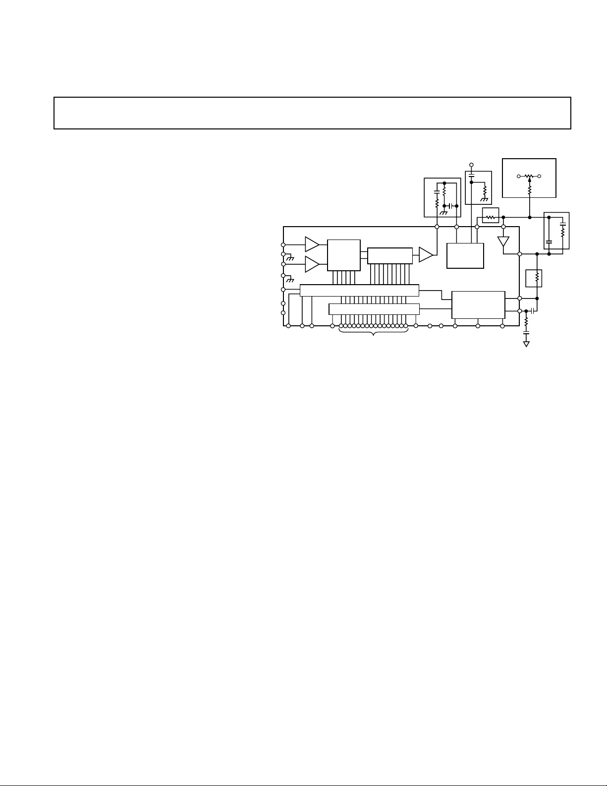
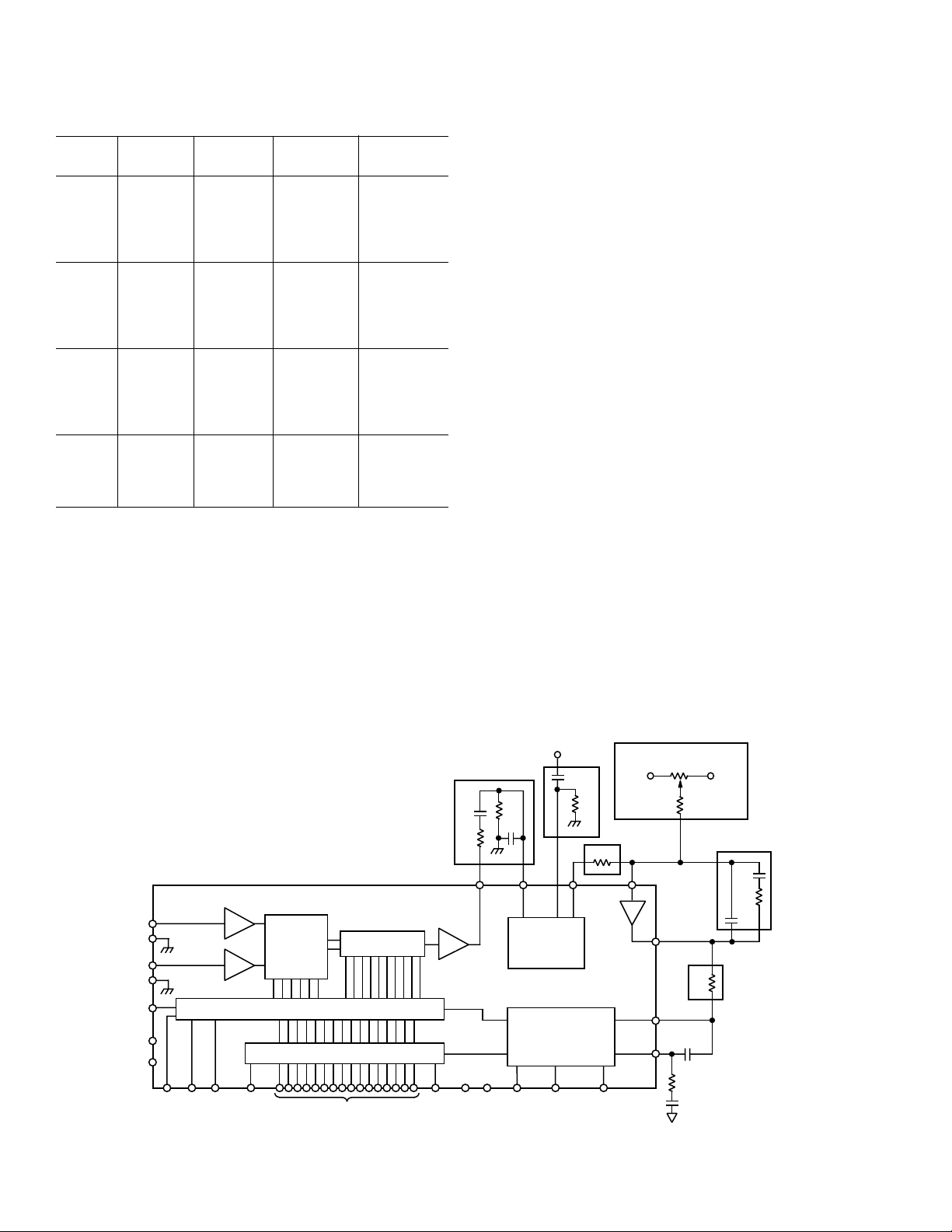
CONNECTING THE CONVERTER
The power supply voltages connected to +VS and –VS pins
should be +12 V dc and –12 V dc and must not be reversed.
The voltage applied to V
can be +5 V dc to +VS.
L
It is recommended that the decoupling capacitors are connected
in parallel between the power lines +V
, –VS and ANALOG
S
GROUND adjacent to the converter. Recommended values are
100 nF (ceramic) and 10 µF (tantalum). Also capacitors of
100 nF and 10 µF should be connected between +V
and
L
DIGITAL GROUND adjacent to the converter.
When more than one converter is used on a card, separate decoupling capacitors should be used for each converter.
The resolver connections should be made to the SIN and COS
inputs, REFERENCE INPUT and SIGNAL GROUND as
shown in Figure 11 and described in the Connecting the
Resolver section.
The two signal ground wires from the resolver should be joined
at the SIGNAL GROUND pin of the converter to minimize the
coupling between the sine and cosine signals. For this reason it
is also recommended that the resolver is connected using individually screened twisted pair cables with the sine, cosine and
reference signals twisted separately.
SIGNAL GROUND and ANALOG GROUND are connected
internally. ANALOG GROUND and DIGITAL GROUND
must be connected externally and as close to the converter as
possible.
The external components required should be connected as
shown in Figure 1.
CONVERTER RESOLUTION
Two major areas of the AD2S83 specification can be selected by
the user to optimize the total system performance. The resolution of the digital output is set by the logic state of the inputs
SC1 and SC2 to be 10, 12, 14 or 16 bits; and the dynamic characteristics of bandwidth and tracking rate are selected by the
choice of external components.
The choice of the resolution will affect the values of R4 and R6
which scale the inputs to the integrator and the VCO respectively (see Component Selection section). If the resolution is
changed, then new values of R4 and R6 must be switched into
the circuit.
Note: When changing resolution under dynamic conditions, do
it when the BUSY is low, i.e., when data is not changing.
SIN
SIG GND
COS
GND
RIPPLE
CLOCK
+12V
–12V
DATA
LOAD
SC1
A1
SEGMENT
SWITCHING
A2
16-BIT UP/DOWN COUNTER
ENABLE
SC2
R - 2R DAC
OUTPUT DATA LATCH
16 DATA BITS
Figure 1. Connection Diagram
AC ERROR O/P
A3
AD2S83
BYTE
SELECT
HF FILTER
C1
R1
5V
GND
R2
C2
PHASE
SENSITIVE
DETECTOR
REFERENCE
I/P
C3
DEMOD
O/P
VCO + DATA
TRANSFER
LOGIC
DIRECTIONBUSYDIG
R3
R4
INTEGRATOR
O/P
INHIBIT
OFFSET ADJUST
+12V
INTEGRATOR
VCO
I/P
VCO
O/P
R9
R8
BANDWIDTH
SELECTION
I/P
R6
C7
150pF
R7
3K3
C6
390pF
–12V
C5
R5
C4
TRACKING
RATE
SELECTION
VELOCITY
SIGNAL
–6–
REV. E
 Loading...