

Low Cost, 14-Bit, Dual Channel
www.BDTIC.com/ADI
Synchro/Resolver-to-Digital Converter
FEATURES
Low per-channel cost
32-lead DIL hybrid package
2.6 arc minute accuracy
14-bit resolution
Built-in test
Independent reference inputs
High tracking rate
APPLICATIONS
Gimbal/gyro control systems
Robotics
Engine controllers
Coordinate conversion
Military servo control systems
Fire control systems
Avionic systems
Antenna monitoring
CNC machine tooling
GENERAL DESCRIPTION
The AD2S44 is a 14-bit dual channel, continuous tracking synchro/
resolver-to-digital converter. It has been designed specifically
for applications where space, weight, and cost are at a premium.
Each 32-lead hybrid device contains two independent Type II servo
loop tracking converters. The ratiometric conversion technique
employed provides excellent noise immunity and tolerance of
long lead lengths.
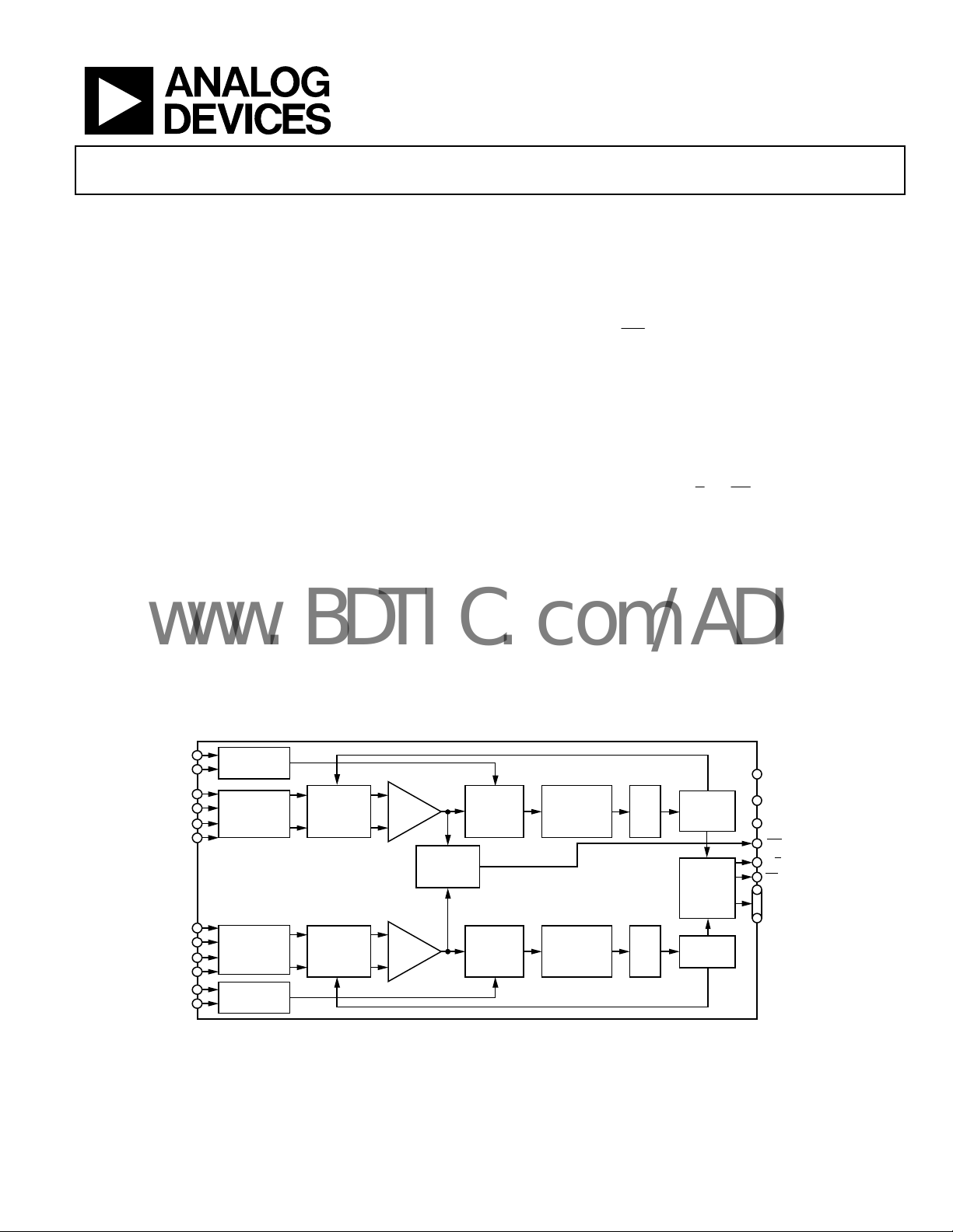
FUNCTIONAL BLOCK DIAGRAM
R
(A)
HI
R
(A)
LO
S1 (A)
S2 (A)
S3 (A)
S4 (A)
S1 (B)
S2 (B)
S3 (B)
S4 (B)
(B)
R
HI
R
(B)
LO
REFERENCE
CONDIT IONE R
SYNCHRO/
RESOLVER
CONDIT IONE R
SYNCHRO/
RESOLVER
CONDIT IONE R
REFERENCE
CONDIT IONE R
AD2S44
HIGH
SPEED
SIN/COS
MULTIPLIER
HIGH
SPEED
SIN/COS
MULTIPLIER
ERROR
AMP
ERROR
AMP
BUILT-IN
TEST
DETECT ION
PHASE-
SENSITIVE
DETECTOR
PHASE-
SENSITIVE
DETECTOR
Figure 1.
AD2S44
The core of each conversion is performed by state-of-the-art monolithic, integrated circuits manufactured by the Analog Devices, Inc.,
proprietary BiMOS II process, which combines the advantages of
low power CMOS digital logic with bipolar linear circuits. The
use of these ICs keeps the internal component count low and
ensures high reliability.
The built-in test (
provide an indication of whether the converter is tracking
accurately.
Each channel incorporates a high accuracy differential conditioning circuit for signal inputs providing more than 74 dB of
common-mode rejection. Options are available for both synchro
and resolver format inputs. The converter output is via a three-state
transparent latch allowing data to be read without interruption of
the converter operation. The A/
channel and present the digital position to the common data
outputs.
The AD2S44 also features independent reference inputs where
different reference frequencies can be used for each channel.
All components are 100% tested at −55°C, +25°C, and +125°C.
Devices are processed to high reliability screening standards
and receive further levels of testing and screening to ensure
high levels of reliability.
INTEGRATOR VCO
INTEGRATOR
BIT
) facility can be used in failsafe systems to
B
and OE control lines select the
+V
S
GND
–V
S
BIT
A/B
OE
DB1 (LSB)
TO
DB14 (MSB)
02947-001
VCO
UP-DOWN
COUNTER
THREE-
STATE
OUTPUT
LATCHES
UP-DOWN
COUNTER
Rev. A
Information furnished by Analog Devices is believed to be accurate and reliable. However, no
responsibility is assumed by Analog Devices for its use, nor for any infringements of patents or other
rights of third parties that may result from its use. Specifications subject to change without notice. No
license is granted by implication or otherwise under any patent or patent rights of Analog Devices.
Trademarks and registered trademarks are the property of their respective owners.
One Technology Way, P.O. Box 9106, Norwood, MA 02062-9106, U.S.A.
Tel: 781.329.4700 www.analog.com
Fax: 781.461.3113 ©1989–2008 Analog Devices, Inc. All rights reserved.

AD2S44
www.BDTIC.com/ADI
TABLE OF CONTENTS
Features .............................................................................................. 1
Applications ....................................................................................... 1
General Description ......................................................................... 1
Functional Block Diagram .............................................................. 1
Table of Contents .............................................................................. 2
Revision History ............................................................................... 2
Specifications ..................................................................................... 3
Absolute Maximum Ratings ............................................................ 5
ESD Caution .................................................................................. 5
Pin Configuration and Function Descriptions ............................. 6
Theory of Operation ........................................................................ 7
Connecting the Converter ........................................................... 7
Channel Select (A/B) ................................................................... 7
REVISION HISTORY
08/08—Rev. 0 to Rev. A
Updated Format .................................................................. Universal
Changes to Specifications Section .................................................. 3
Changes to Absolute Maximum Ratings Section ......................... 5
Deleted Standard Processing Section ............................................. 7
Output Enable (OE) ......................................................................8
Built-In Test (
Scaling for Nonstandard Signals .................................................9
Dynamic Performance ..................................................................9
Acceleration Error .........................................................................9
Reliability ..................................................................................... 10
Processing for High Reliability (B Suffix) ............................... 10
Other Products ........................................................................... 10
Outline Dimensions ....................................................................... 11
Ordering Guide .......................................................................... 11
Ordering Information ................................................................ 11
Changes to Processing for High Reliability Section and
Other Products Section ................................................................. 10
Updated Outline Dimensions ....................................................... 11
Changes to Ordering Guide .......................................................... 11
Changes to Ordering Information ............................................... 11
10/89—Revision 0: Initial Version
BIT
) .........................................................................8
Rev. A | Page 2 of 12

AD2S44
www.BDTIC.com/ADI
SPECIFICATIONS
VS = ±15 V at TA = 25°C, unless otherwise noted.
Table 1.
Parameter Min Typ Max Unit Test Conditions/Comments
PERFORMANCE
Accuracy
Tracking Rate 20 Rev/sec
Resolution (1 LSB = 1.3 Arc Minutes) 14 Bits Output coding parallel natural binary
Repeatability 1 LSB
Signal/Reference Frequency 400 2600 Hz
Bandwidth 100 Hz
SIGNAL INPUTS
Signal Voltage 11.8 or 90 V rms See the Ordering Information section
Input Impedance
Common-Mode Rejection 74 dB
Common-Mode Range
REFERENCE INPUTS
Reference Voltage 26 or 115 V rms See the Ordering Information section
Input Impedance
Common-Mode Range
ACCELERATION CONSTANT 62,000 sec
STEP RESPONSE
Large Step
Small Step
POWER LINES
+VS = +15 V
–VS = −15 V
Power Dissipation 1.7 1.9 W Quiescent condition
DIGITAL INPUTS
OE
A/B
DIGITAL OUTPUTS (DB1 to DB14)
V
V
Three-State Leakage Current ±40 μA
Drive Capability 3 LSTTL loads
1
AD2S44-UMB
2
−4.0 +4.0 Arc minutes −55°C to +125°C
−2.6 +2.6 Arc minutes −25°C to +85°C
AD2S44-TMB
2
−4.0 +4.0 Arc minutes −55°C to +125°C
90 V Signal 200 kΩ Resistive tolerance ±2%
11.8 V Signal 26 kΩ
90 V Signal ±250 V dc
11.8 V Signal ±60 V dc
115 V 270 kΩ Resistive tolerance ±5%
26 V 270 kΩ
115 V ±210 V dc
26 V ±210 V dc
–2
1, 2
1, 2
25 30 ms 2° to 1 LSB of error
1, 2
1, 2
63 75 ms 179° to 1 LSB of error
75 80 mA Quiescent condition
40 45 mA Quiescent condition
VIL 0.7 V dc IIL = 5 μA
VIH 2.0 V dc IIH = 5 μA
VIL 0.7 V dc IIL = 1.2 mA
VIH 2.0 V dc IIH = –60 μA
1, 2
OL
1, 2
OH
0.4 V dc IIL = 1.2 mA
2.4 V dc IOH = 60 μA
Rev. A | Page 3 of 12

AD2S44
www.BDTIC.com/ADI
Parameter Min Typ Max Unit Test Conditions/Comments
DATA TRANSFER See Figure 6
Time to Data Stable (After Negative Edge of OE
or Change of Level of A/B)
Time to Data in High Impedance State
(After Positive Edge of OE
Time for Repetitive Strobing of Selected Channel 200 ns tP
BUILT-IN TEST OUTPUT (BIT)
Sense Active low Low = error condition
VOL 0.4 V dc IOL = 3.2 mA
VOH 2.4 V dc IOH = −160 μA
Drive Capability 8 LSTTL loads
Error Condition Set 55 LSB
Error Condition Cleared 45 LSB
1
Specified overtemperature range, −55°C to +125°C, and for: (a) ±10% signal and reference amplitude variation; (b) ±10% signal and reference harmonic distortion; (c)
±5% power supply variation; and (d) ±10% variation in reference frequency.
2
These parameters are 100% tested at nominal values of power supplies, input signal voltages, and operating frequency. All other parameters are guaranteed by
design, not tested.
)
640 ns t
200 ns t
S
R
Rev. A | Page 4 of 12

AD2S44
www.BDTIC.com/ADI
ABSOLUTE MAXIMUM RATINGS
Table 2.
Parameter Rating
+VS to GND +17.25 V dc
–VS to GND −17.25 V dc
Any Logic Input to GND +6.0 V dc (maximum)
Any Logic Input to GND −0.4 V dc (minimum)
Maximum Junction Temperature 150°C
S1, S2, S3, S4 Pins (Line-to-Line)
90 V Option ±600 V dc
11.8 V Option ±80 V dc
S1, S2, S3, S4 Pins to GND
90 V Option ±600 V dc
11.8 V Option ±80 V dc
RHI Pins to RLO Pins
26 V, 115 V Options ±600 V dc
RHI Pins to RLO Pins to GND
26 V, 115 V Options ±600 V dc
Storage Temperature Range −65°C to +150°C
Operating Temperature Range −55°C to +125°C
1
On synchro input options, line-to-line voltage refers to the differential voltages
of S2 (A)/S2 (B) to S1 (A)/S1 (B), S1 (A)/S1 (B) to S3 (A)/S3 (B), and S3 (A)/S3 (B)
to S2 (A)/S2 (B). On resolver input options, line-to-line levels refer to the S1 (A)/
S1 (B) to S3 (A)/S3 (B) and S2 (A)/S2 (B) to S4 (A)/S4 (B) voltages.
1
Stresses above those listed under Absolute Maximum Ratings
may cause permanent damage to the device. This is a stress
rating only; functional operation of the device at these or any
other conditions above those indicated in the operational
section of this specification is not implied. Exposure to absolute
maximum rating conditions for extended periods may affect
device reliability.
ESD CAUTION
Rev. A | Page 5 of 12

AD2S44
www.BDTIC.com/ADI
PIN CONFIGURATION AND FUNCTION DESCRIPTIONS
1
DB8
2
DB9
3
DB10
4
DB11
5
DB12
6
DB13
DB14 (LSB)
7
AD2S44
8
OE
A/B
BIT
(A)
R
LO
R
(A)
HI
S4 (A) S4 (B)
S3 (A)
S2 (A) S2 (B)
S1 (A) S1 (B)
9
(Not to Scale)
10
11
12
13
14
15
16
TOP VIEW
Figure 2. Pin Configuration
Table 3. Pin Function Descriptions
Pin No. Mnemonic Description
1 to 7 DB8 to DB14 (LSB) Parallel Output Data Bits.
8
9
10
OE
A/B
BIT
Output Enable Input.
Channel A or Channel B Select Input.
Built-In Test Error Output.
11 RLO (A) Input Pin for Channel A Reference Low.
12 RHI (A) Input Pin for Channel A Reference High.
13 to 16 S4 (A) to S1 (A) Channel A Input Signal.
17 to 20 S1 (B) to S4 (B) Channel B Input Signal.
21 RHI (B) Input Pin for Channel B Reference High.
22 RLO (B) Input Pin for Channel B Reference Low.
23 GND Power Supply Ground. This pin is electrically connected to the case.
24 –VS Negative Power Supply.
25 +VS Positive Power Supply.
26 to 32 DB1 (MSB) to DB7 Parallel Output Data Bits.
32
DB7
31
DB6
30
DB5
29
DB4
28
DB3
27
DB2
26
DB1 (MSB)
25
+V
24
–V
23
GND
22
R
21
R
20
19
S3 (B)
18
17
S
S
(B)
LO
(B)
HI
02947-003
Rev. A | Page 6 of 12

AD2S44
www.BDTIC.com/ADI
THEORY OF OPERATION
The AD2S44 operates on a tracking principle. The output digital
word continually tracks the position of the synchro/resolver shaft
without the need for external convert commands and status wait
loops. As the transducer moves through a position equivalent
to the least significant bit weighting, the output digital word is
updated.
Each channel is identical in operation, sharing power supply and
output pins. Both channels operate continuously and independently of each other. The digital output from either channel is
available after switching the channel select and output enable
inputs.
If the device is a synchro-to-digital converter, the 3-wire synchro
output is connected to the S1, S2, and S3 pins on the unit, and
a solid-state Scott T input conditioner converts these signals into
resolver format given by
V
= K E0 sin ωt sin θ
1
V
= K E0 sin ωt cos θ
2
where:
θ is the angle of the synchro shaft.
E
sin ωt is the reference signal.
0
K is the transformation ratio of the input signal conditioner.
If the unit is a resolver-to-digital converter, the 4-wire resolver
output is connected directly to the S1, S2, S3, and S4 pins on
the unit.
To understand the conversion process, assume that the current
word state of the up-down counter is ϕ. V
and V
is multiplied by sin ϕ to give the following:
2
sin ωt sin θ cos ϕ
K E
0
K E
sin ωt cos θ sin ϕ
0
is multiplied by cos ϕ,
1
These signals are subtracted by the error amplifier to give
K E
sin ωt (sin θ cos ϕ − cos θ sin ϕ)
0
or
K E
sin ωt sin (θ − ϕ)
0
R
(A)
HI
R
LO
S1 (A)
S2 (A)
S3 (A)
S4 (A)
S1 (B)
S2 (B)
S3 (B)
S4 (B)
R
HI
R
LO
(A)
(B)
(B)
REFERENCE
CONDITI ONER
SYNCHRO/
RESOLVER
CONDITI ONER
SYNCHRO/
RESOLVER
CONDITI ONER
REFERENCE
CONDITI ONER
V
1
MULTIPLIER
V
2
AD2S44
MULTIPLIER
HIGH
SPEED
SIN/CO S
HIGH
SPEED
SIN/CO S
ERROR
AMP
BUILT-IN
TEST
DETECTION
ERROR
AMP
Figure 3. Functional Block Diagram
SENSITIVE
DETECTO R
SENSITIVE
DETECTO R
A phase sensitive detector, integrator, and voltage-controlled
oscillator (VCO) form a closed-loop system that seeks to null sin
(θ − ϕ). When this is accomplished, the word state of the up-down
counter (ϕ) equals the synchro/resolver shaft angle (θ), to within
the rated accuracy of the converter.
CONNECTING THE CONVERTER
The power supply voltages connected to −VS and +VS are to be
±15 V and cannot be reversed.
It is suggested that a parallel combination of a ceramic 100 nF
capacitor and a tantalum 6.8 μF capacitor be placed from each
of the supply pins to GND.
The pin marked GND is connected electrically to the case and
is to be taken to 0 V potential in the system.
The digital output is taken from Pin 26 to Pin 32 and from Pin 1
to Pin 7. Pin 26 is the MSB, and Pin 7 is the LSB.
The reference connections are made to the R
pins and the RLO
HI
pins. In the case of a synchro, the signals are connected to the
S1, S2, and S3 pins, according to the following convention:
E
E
E
S1−S3
S3−S2
S2−S1
= E
= E
= E
sin ωt sin θ
RLO−RHI
sin ωt sin (θ − 120°)
RLO−RHI
sin ωt sin (θ – 240°)
RLO−RHI
For a resolver, the signals are connected to the S1, S2, S3, and S4
pins, according to the following convention:
E
E
S1−S3
S2−S4
= E
= E
RLO−RHI
RLO−RHI
sin ωt sin θ
sin ωt cos θ
CHANNEL SELECT (A/B)
A/B is the channel select input. A Logic 1 selects Channel A, and
a Logic 0 selects Channel B. Data becomes valid 640 ns after A/
is toggled. Timing information is shown in and . Figure 4 Figure 5
+V
S
PHASE-
PHASE-
INTEGRATOR VCO
INTEGRATOR
VCO
UP-DOWN
COUNTER
THREE-
STATE
OUTPUT
LATCHES
UP-DOWN
COUNTER
GND
–V
S
BIT
A/B
OE
DB1 (LSB)
TO
DB14 (MSB)
02947-010
B
Rev. A | Page 7 of 12

AD2S44
www.BDTIC.com/ADI
OUTPUT ENABLE (OE)
OE
is the output enable input; the signal is active low. When set
to Logic 1, DB1 to DB14 are in high impedance state. When
is set to Logic 0, DB1 to DB14 represent the angle of the transducer
shaft to within the stated accuracy of the converter (see bit weights
in ). Data becomes valid 640 ns after the Tabl e 4
Timing information is shown in and and
detailed in .
Tabl e 1
Figure 4 Figure 5
OE
is switched.
Table 4. Bit Weight
Bit No. Weight (Degrees)
1 (MSB) 180.0000
2 90.0000
3 45.0000
4 22.5000
5 11.2500
6 5.6250
7 2.8125
8 1.4063
9 0.7031
10 0.3516
11 0.1758
12 0.0879
13 0.0439
14 ( LSB) 0.0220
OE
A/B
t
S
DATA
BITS
(1 TO 14)
*CONVERT ER DATA OUTPUT I S INHIBITED F ROM UPDATES
DURING CHANNE L VALID.
Figure 4. Repetitive Reading of One Channel
CHANNEL B
VAL ID*
t
S
CHANNEL A
VAL ID*
OE
t
R
02947-005
BUILT-IN TEST (BIT)
BIT
The
velocity or fault indication signal for the channel selected via A/
The error voltage of each channel is continuously monitored. When
the error exceeds ±50 bits for the currently selected channel, the
BIT
imately one angular degree exists, and the data is, therefore, invalid.
The
set the
The
the error goes below 45 LSBs. This mode of operation guarantees
that the
The
the change in the state of A/
tion that sets the
reference signal prior to the
Table 5.
Condition Description
Power-Up Transient
Response
Step Input > 1°
Excessive Velocity
Signal Failure
Converter/System
Fai lure
is the built-in test error output, which provides an over-
B
.
output goes low, indicating that an error greater than approx-
BIT
signal has a built-in hysteresis; that is, the error required to
BIT
is greater than the error required for it to be cleared.
BIT
is set when the error exceeds 55 LSBs and is cleared when
BIT
does not flicker when the error threshold is crossed.
BIT
is valid for the selected channel approximately 50 ns after
B
. In most instances, the error condi-
BIT
must persist for at least one period of the
BIT
responding to the condition.
BIT
Output Faults
The BIT returns to a logic high state after
the AD2S44 position output synchronizes
with the angle input to within 1°.
Normally, the BIT is low at power-up for
a period less than or equal to the large
signal step response settling time of the
AD2S44 after the ±VS supplies have
stabilized to within 5% of their final values.
returns to a logic high state after
The BIT
the selected channel of the AD2S44 has
settled to within 1° of the input angle
resulting from an instantaneous step.
is driven to a logic low if the
The BIT
maximum tracking rate of the AD2S44 is
exceeded (20 rps typical).
may be driven to a logic low state if
The BIT
all signal voltages to the selected channel
are lost.
Any failure that causes the AD2S44 to fail
to track the input synchro/resolver angles
drives the BIT
to a logic low. This may
include, but is not limited to, acceleration
conditions, poor supply voltage regulation,
or excessive noise on the signal connections.
OE
t
P
A/B
DATA
VAL ID *
t
R
DATA
VAL ID*
02947-004
Rev. A | Page 8 of 12
t
S
DATA
BITS
(1 TO 14)
*CONVERTER DATA OUT PUT IS I NHIBITED FRO M UPDATES
DURING CHANNE L VALID.
Figure 5. Alternative Reading of Each Channel

AD2S44
www.BDTIC.com/ADI
SCALING FOR NONSTANDARD SIGNALS
A feature of these converters is that the signal and reference inputs
can be resistively scaled to accommodate nonstandard input signal
and reference voltages that are outside the nominal ±10% limits of
the converter. Using this technique, it is possible to use a standard
converter with a personality card in systems where a wide range
of input and reference voltages are encountered.
The accuracy of the converter is affected by the matching accuracies of resistors used for external scaling. For resolver format
options, it is critical that the value of the resistors on the S1 (A)/
S1 (B) to S3 (A)/S3 (B) signal input pair be precisely matched to
the S4 (A)/S4 (B) to S2 (A)/S2 (B) input pair. For synchro options,
the three resistors on the S1, S2, and S3 pins must be matched. In
general, a 0.1% mismatch between resistor values contributes an
additional 1.7 arc minutes of error to the conversion. In addition,
imbalances in resistor values can greatly reduce the commonmode rejection ratio of the signal inputs.
To calculate the values of the external scaling resistors, add
2.222 kΩ for each volt of signal in series with the S1, S2, S3, and
S4 pins (no resistor is required on the S4 pins for synchro options)
and add 3 kΩ extra per volt of reference in series with the R
LO
pins and the RHI pins.
DYNAMIC PERFORMANCE
θ
IN
Figure 6. Transfer Function of AD2S44
K
S
The transfer function of the converter is as follows:
Open-loop transfer function
1 + sT
a
2
1 + sT
1
2
θ
OUT
02947-006
The gain and phase diagrams are shown in Figure 7 and Figure 8.
6
3
0
–3
–6
GAIN (dB)
–9
–12
–15
10 100
180
135
90
45
0
–45
PHASE (Degrees)
–90
–135
–180
10 100
FREQUENCY ( Hz)
Figure 7. Gain Plot
FREQUENCY ( Hz)
Figure 8. Phase Plot
02947-007
02947-008
sT
+
θ
OUT
θ
IN
1
K
a
2
s
1
×=
sT
+
1
2
Closed-loop transfer function
sT
1
θ
OUT
=
1
θ
IN
+
where:
= 62000 sec–2.
K
a
= 0.0061 sec.
T
1
= 0.001 sec.
T
2
ACCELERATION ERROR
A tracking converter employing a Type II servo loop does not
suffer any velocity lag. However, there is an additional error
due to acceleration. This error is defined using the acceleration
1
32
+++
KTsKssT
a2a1
constant (K
The numerator and denominator must have consistent angular
units. For example, if K
tion is to be specified in degrees/sec
to be specified in degrees. Alternatively, the angular unit of measure
can also be in units such as radians, arc minutes, or LSBs.
Rev. A | Page 9 of 12
) of the converter
a
K
= Input Acceleration/Error in Output Angle
a
is expressed in sec–2, the input accelera-
a
2
and the output angle error is

AD2S44
www.BDTIC.com/ADI
Ka does not define maximum acceleration; it defines only the
error due to acceleration. The maximum acceleration of which
the AD2S44 keeps track is approximate to 5 × K
2
or about 800 revolutions/sec
can be used to predict the output position error due to input
K
a
.
= 310,000°/sec2
a
acceleration. For example, an acceleration of 50 revolutions/sec
= 62,000 is calculated using the following equation:
with K
a
LSB
⎤
⎡
onAcceleratiInput
2
⎥
⎢
sec
⎦
50
LSBsinErrors
=
LSBrev
⎡
⎤
⎡
⎢
sec
⎣
14
×
2
2
⎢
⎥
⎦
rev
⎣
2
−
[]
sec000,62
K
a
⎤
⎥
⎦
=
2.13
⎣
−2
[]
sec
LSBs
=
2
PROCESSING FOR HIGH RELIABILITY (B SUFFIX)
As a part of the high reliability manufacturing procedure, all
converters receive the processing shown in Tab l e 6 .
Table 6.
Process1 Conditions
Precap Visual Inspection MIL-STD-883, Method 2017
Temperature Cycling 10 cycles, –65°C to +150°C
Constant Acceleration 5000 Gs, Y1 plane
Interim Electrical Tests @ 25°C
Operating Burn In 160 hours @ 125°C
Seal Test, Fine and Gross MIL-STD-883, Method 1014
Final Electrical Test Performed at T
External Visual Inspection MIL-STD-883, Method 2009
1
Test and screening data supplied by request.
MIN
, T
, T
AMB
MAX
RELIABILITY
The reliability of these products is very high due to the extensive
use of custom chip circuits that decrease the active component
count. Calculations of the MTBF figure under various environmental conditions are available upon request from Analog
Devices.
Figure 9 shows the MTBF in years vs. case temperature for
Naval Sheltered conditions calculated in accordance with the
Mil-Hdbk-217E.
100
10
MTBF (Years)
1
25 6545 85 105 125
Figure 9. MTBF vs. Temperature
TEMPERATURE (°C)
02947-009
OTHER PRODUCTS
Analog Devices manufactures many other products concerned
with the conversion of synchro/resolver data, such as the
SDC/RDC1740 series and the AD2S80A series.
Hybrid
The SDC/RDC1740 is a hybrid synchro/resolver-to-digital
converter with internal isolating micro transformers.
Monolithic
The AD2S80A series are ICs performing resolver-to-digital
conversion with accuracies up to ±2 arc minutes and 16-bit
resolution.
Rev. A | Page 10 of 12

AD2S44
www.BDTIC.com/ADI
OUTLINE DIMENSIONS
1.728 (43.89) MAX
1732
1.102 (27.99)
1.079 (27.41)
0.225 (5.72)
MAX
0.192 (4.88)
0.152 (3.86)
0.025 (0.64)
1
PIN 1
INDICATOR
(NOTE 1)
MIN
0.023 (0.58)
0.014 (0.36)
0.100 (2.54)
BSC
0.070 (1.78)
0.030 (0.76)
NOTES:
1. INDEX AREA IS INDICATED BY A NOTCH OR LEAD ONE
IDENTIFICATION MARK LOCATED ADJACENT TO LEAD ONE.
2. CONTROLLING DIMENSION S ARE IN INCHES. MILLIMETER DIMENSIONS
(IN PARENTHESES) ARE ROUNDED-OFF INCH EQUIVALENTS FOR
REFERENCE ONLY AND ARE NOT APPROPRIATE FOR USE IN DESIGN.
0.025 (0.64)
0.015 (0.38)
16
0.206 (5.23)
0.186 (4.72)
0.120 (3.05)
MAX
0.910 (23.11)
0.890 (22.61)
0.015 (0.38)
0.008 (0.20)
Figure 10. 32-Lead Bottom-Brazed Ceramic DIP for Hybrid [BBDIP_H]
(DH-32E)
Dimensions shown in inches and (millimeters)
ORDERING GUIDE
Model Temperature Range Package Description Package Option
AD2S44–TM11B −55°C to +125°C 32-Lead Bottom-Brazed Ceramic DIP for Hybrid [BBDIP_H] DH-32E
AD2S44–TM12B −55°C to +125°C 32-Lead Bottom-Brazed Ceramic DIP for Hybrid [BBDIP_H] DH-32E
AD2S44–TM18B −55°C to +125°C 32-Lead Bottom-Brazed Ceramic DIP for Hybrid [BBDIP_H] DH-32E
AD2S44–UM18B −55°C to +125°C 32-Lead Bottom-Brazed Ceramic DIP for Hybrid [BBDIP_H] DH-32E
ORDERING INFORMATION
When ordering, the converter part numbers are to be suffixed by
a two-letter code defining the accuracy grade, and a two digit
numeric code defining the signal/reference voltage and frequency.
All the standard options, and their option codes, are shown in
Figure 11. For nonstandard configurations, contact Analog
Devices.
For example, the AD2S44–TM12B is the correct part number
for a component that operates with 90 V signal, 115 V reference
synchro format inputs and yields a ±4.0 arc minutes accuracy
over the −55°C to +125°C temperature range processed to high
reliability standards.
Rev. A | Page 11 of 12
AD2S44-
BASE PART
*MODEL I S OBSOLETE AND NO LONG ER AVAILABLE.
NUMBER
XM Y BZ
HIGH-REL PRO CESSING
Z = 0* SIGNAL, 2V REFERENCE, 2V RESOLVE R
Z = 1 SIGNAL, 1 1.8V REFE RENCE, 26V S YNCHRO
Z = 2 SIGNAL, 9 0V REFERENCE, 115V SYNCHRO
Z = 3* SIGNAL, 11. 8V REFERENCE, 11. 8V RESOLVER
Z = 4* SIGNAL, 26V REFERENCE, 26V RESOLVER
BASE PART
Z = 8 SIGNAL, 1 1.8V REFE RENCE, 26V RE SOLVER
Y = 1 400Hz TO 2 .6kHz REFERENCE FREQUENCY
X = U –55°C TO +1 25°C OPERAT ING TEM PERATURE
RANGE
±4.0 ARC M IN ACCURACY
±2.6 ARC M IN ACCURACY ( –25°C TO +85°C)
X = T –55°C TO +125°C OPERATI NG TEMPE RATURE
RANGE±4 .0 ARC MI N ACCURACY
X = S* –55°C TO +1 25°C OPERATING TEMPERATURE
RANGE±5 .2 ARC MI N ACCURACY
Figure 11.
02947-002

AD2S44
www.BDTIC.com/ADI
NOTES
©1989–2008 Analog Devices, Inc. All rights reserved. Trademarks and
registered trademarks are the property of their respective owners.
D02947-0-8/08(A)
Rev. A | Page 12 of 12
 Loading...