

Variable Resolution, 10-Bit to 16-Bit R/D
www.BDTIC.com/ADI
FEATURES
Complete monolithic resolver-to-digital converter
3125 rps maximum tracking rate (10-bit resolution)
±2.5 arc minutes of accuracy
10-/12-/14-/16-bit resolution, set by user
Parallel and serial 10-bit to 16-bit data ports
Absolute position and velocity outputs
System fault detection
Programmable fault detection thresholds
Differential inputs
Incremental encoder emulation
Programmable sinusoidal oscillator on-board
Compatible with DSP and SPI interface standards
5 V supply with 2.3 V to 5 V logic interface
−40°C to +125°C temperature rating
APPLICATIONS
DC and ac servo motor control
Encoder emulation
Electric power steering
Electric vehicles
Integrated starter generators/alternators
Automotive motion sensing and control
Converter with Reference Oscillator
AD2S1210
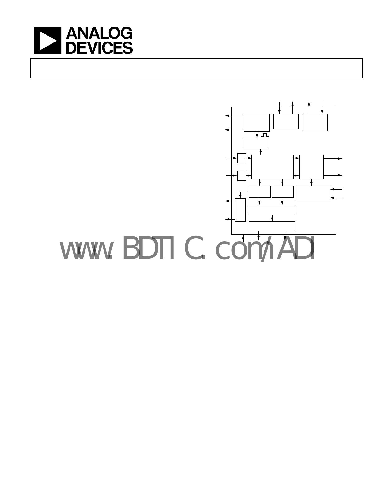
FUNCTIONAL BLOCK DIAGRAM
EXCITATION
OUTPUTS
INPUTS
FROM
RESOLVER
ENCODER
EMULATION
OUTPUTS
REFERENCE
OSCILLATOR
SYNTHETIC
REFERENCE
ADC
ADC
ENCODER
EMULATION
RESET
(DAC)
TYPE II
TRACKING LO OP
POSITION
REGISTER
MULTIPLEXER
DATA BUS OUTPUT
DATA I/O
REFERENCE
PINS
VOLTAGE
REFERENCE
VELOCITY
REGISTER
Figure 1.
CRYSTAL
INTERNAL
GENERATOR
AD2S1210
FAULT
DETECT ION
CONFIGURATION
REGISTER
CLOCK
FAULT
DETECTION
OUTPUTS
DATA I/O
07467-001
GENERAL DESCRIPTION
The AD2S1210 is a complete 10-bit to 16-bit resolution tracking
resolver-to-digital converter, integrating an on-board programmable sinusoidal oscillator that provides sine wave excitation
for resolvers.
The converter accepts 3.15 V p-p ± 27% input signals, in the range
of 2 kHz to 20 kHz on the sine and cosine inputs. A Type II
servo loop is employed to track the inputs and convert the input
sine and cosine information into a digital representation of the
input angle and velocity. The maximum tracking rate is 3125 rps.
Rev. 0
Information furnished by Analog Devices is believed to be accurate and reliable. However, no
responsibility is assumed by Analog Devices for its use, nor for any infringements of patents or other
rights of third parties that may result from its use. Specifications subject to change without notice. No
license is granted by implication or otherwise under any patent or patent rights of Analog Devices.
Trademarks and registered trademarks are the property of their respective owners.
PRODUCT HIGHLIGHTS
1. Ratiometric tracking conversion. The Type II tracking loop
provides continuous output position data without
conversion delay. It also provides noise immunity and
tolerance of harmonic distortion on the reference and
input signals.
2. System fault detection. A fault detection circuit can sense
loss of resolver signals, out-of-range input signals, input
signal mismatch, or loss of position tracking. The fault
detection threshold levels can be individually programmed
by the user for optimization within a particular application.
3. Input signal range. The sine and cosine inputs can accept
differential input voltages of 3.15 V p-p ± 27%.
4. Programmable excitation frequency. Excitation frequency
is easily programmable to a number of standard frequencies
between 2 kHz and 20 kHz.
5. Triple format position data. Absolute 10-bit to 16-bit angular
position data is accessed via either a 16-bit parallel port or a
4-wire serial interface. Incremental encoder emulation is in
standard A-quad-B format with direction output available.
6. Digital velocity output. 10-bit to 16-bit signed digital velocity
accessed via either a 16-bit parallel port or a 4-wire serial
interface.
One Technology Way, P.O. Box 9106, Norwood, MA 02062-9106, U.S.A.
Tel: 781.329.4700 www.analog.com
Fax: 781.461.3113 ©2008 Analog Devices, Inc. All rights reserved.

AD2S1210
www.BDTIC.com/ADI
TABLE OF CONTENTS
Features .............................................................................................. 1
Applications ....................................................................................... 1
Functional Block Diagram .............................................................. 1
General Description ......................................................................... 1
Product Highlights ........................................................................... 1
Revision History ............................................................................... 2
Specifications ..................................................................................... 3
Timing Specifications .................................................................. 6
Absolute Maximum Ratings ............................................................ 8
ESD Caution .................................................................................. 8
Pin Configuration and Function Descriptions ............................. 9
Typical Performance Characteristics ........................................... 11
Resolver Format Signals ................................................................. 15
Theory of Operation ...................................................................... 16
Resolver to Digital Conversion ................................................. 16
Fault Detection Circuit .............................................................. 16
On-Board Programmable Sinusoidal Oscillator .................... 18
Synthetic Reference Generation ............................................... 18
Configuration of AD2S1210 ......................................................... 20
Modes of Operation ................................................................... 20
Register Map .................................................................................... 21
Position Register ......................................................................... 21
Velocity Register ......................................................................... 21
REVISION HISTORY
8/08—Revision 0: Initial Version
LOS Threshold Register ............................................................ 21
DOS Overrange Threshold Register ........................................ 21
DOS Mismatch Threshold Register ......................................... 21
DOS Reset Maximum and Minimum Threshold Registers . 22
LOT High Threshold Register .................................................. 22
LOT Low Threshold Register ................................................... 22
Excitation Frequency Register .................................................. 22
Control Register ......................................................................... 22
Software Reset Register ............................................................. 23
Fault Register .............................................................................. 23
Digital interface .............................................................................. 24
SOE
Input .................................................................................... 24
SAMPLE
Data Format ................................................................................ 24
Parallel Interface ......................................................................... 24
Serial Interface ............................................................................ 28
Incremental Encoder Outputs .................................................. 31
Supply Sequencing and Reset ................................................... 31
Circuit Dynamics ........................................................................... 32
Loop Response Model ............................................................... 32
Sources of Error .......................................................................... 33
Outline Dimensions ....................................................................... 34
Ordering Guide .......................................................................... 34
Input............................................................................ 24
Rev. 0 | Page 2 of 36

AD2S1210
www.BDTIC.com/ADI
SPECIFICATIONS
MIN
EXC
frequency = 10 kHz to 20 kHz (10-bit); 6 kHz to 20 kHz (12-bit);
to T
; unless otherwise noted.1
MAX
COS to COSLO
AVDD = DVDD = 5.0 V ± 5%, CLKIN = 8.192 MHz ± 25%, EXC,
3 kHz to 12 kHz (14-bit); 2 kHz to 10 kHz (16-bit); T
= T
A
Table 1.
Parameter Min Typ Max Unit Conditions/Comments
SINE, COSINE INPUTS2
Voltage Amplitude 2.3 3.15 4.0 V p-p Sinusoidal waveforms, differential SIN to SINLO,
Input Bias Current 8.25 μA VIN = 4.0 V p-p, CLKIN = 8.192 MHz
Input Impedance 485 kΩ VIN = 4.0 V p-p, CLKIN = 8.192 MHz
Phase Lock Range −44 +44 Degrees Sine/cosine vs. EXC output, Control Register D3 = 0
Common-Mode Rejection ±20 arc sec/V 10 Hz to 1 MHz, Control Register D4 = 0
ANGULAR ACCURACY3
Angular Accuracy ±2.5 + 1 LSB ±5 + 1 LSB arc min B, D grades
±5 + 1 LSB ±10 + 1 LSB arc min A, C grades
Resolution 10, 12, 14, 16 Bits No missing codes
Linearity INL
10-bit ±1 LSB B, D grades
±2 LSB A, C grades
12-bit ±2 LSB B, D grades
±4 LSB A, C grades
14-bit ±4 LSB B, D grades
±8 LSB A, C grades
16-bit ±16 LSB B, D grades
±32 LSB A, C grades
Linearity DNL ±0.9 LSB
Repeatability ±1 LSB
VELOCITY OUTPUT
Velocity Accuracy4
10-bit ±2 LSB B, D grades, zero acceleration
±4 LSB A, C grades, zero acceleration
12-bit ±2 LSB B, D grades, zero acceleration
±4 LSB A, C grades, zero acceleration
14-bit ±4 LSB B, D grades, zero acceleration
±8 LSB A, C grades, zero acceleration
16-bit ±16 LSB B, D grades, zero acceleration
±32 LSB A, C grades, zero acceleration
Resolution5 9, 11, 13, 15 Bits
DYNAMNIC PERFORMANCE
Bandwidth
10-bit 2000 6500 Hz
2900 5300 Hz CLKIN = 8.192 MHz
12-bit 900 2800 Hz
1200 2200 Hz CLKIN = 8.192 MHz
14-bit 400 1500 Hz
600 1200 Hz CLKIN = 8.192 MHz
16-bit 100 350 Hz
125 275 Hz CLKIN = 8.192 MHz
Rev. 0 | Page 3 of 36

AD2S1210
www.BDTIC.com/ADI
Parameter Min Typ Max Unit Conditions/Comments
Tracking Rate
10-bit 3125 rps CLKIN = 10.24 MHz
2500 CLKIN = 8.192 MHz
12-bit 1250 rps CLKIN = 10.24 MHz
1000 CLKIN = 8.192 MHz
14-bit 625 rps CLKIN = 10.24 MHz
500 CLKIN = 8.192 MHz
16-bit 156.25 rps CLKIN = 10.24 MHz
125 CLKIN = 8.192 MHz
Acceleration Error
10-bit 30 arc min At 50,000 rps2, CLKIN = 8.192 MHz
12-bit 30 arc min At 10,000 rps2, CLKIN = 8.192 MHz
14-bit 30 arc min At 2500 rps2, CLKIN = 8.192 MHz
16-bit 30 arc min At 125 rps2, CLKIN = 8.192 MHz
Settling Time 10° Step Input
10-bit 0.6 0.9 ms To settle to within ±2 LSB , CLKIN = 8.192 MHz
12-bit 2.2 3.1 ms To settle to within ±2 LSB, CLKIN = 8.192 MHz
14-bit 6.5 9.0 ms To settle to within ±2 LSB , CLKIN = 8.192 MHz
16-bit 27.5 40 ms To settle to within ±2 LSB, CLKIN = 8.192 MHz
Settling Time 179° Step Input
10-bit 1.5 2.2 ms To settle to within ±2 LSB , CLKIN = 8.192 MHz
12-bit 4.75 6.0 ms To settle to within ±2 LSB, CLKIN = 8.192 MHz
14-bit 10.5 14.7 ms To settle to within ±2 LSB , CLKIN = 8.192 MHz
16-bit 45 66 ms To settle to within ±2 LSB, CLKIN = 8.192 MHz
EXC
EXC,
VOLTAGE REFERENCE
CLKIN, XTALOUT6
LOGIC INPUTS
LOGIC OUTPUTS
OUTPUTS
Voltage 3.2 3.6 4.0 V p-p Load ±100 μA, typical differential output
Center Voltage 2.40 2.47 2.53 V
Frequency 2 20 kHz
EXC
EXC/
EXC/
THD −58 dB First five harmonics
REFOUT 2.40 2.47 2.53 V ±I
Drift 100 ppm/°C
PSRR −60 dB
VIL Voltage Input Low 0.8 V
VIH Voltage Input High 2.0 V
VIL Voltage Input Low 0.8 V V
0.7 V V
VIH Voltage Input High 2.0 V V
1.7 V V
IIL Low Level Input Current (Non
IIL Low Level Input Current (Pull-Up) 80 μA
IIH High Level Input Current −10 μA
VOL Voltage Output Low 0.4 V V
VOH Voltage Output High 2.4 V V
2.0 V V
I
I
DC Mismatch
EXC
AC Mismatch
Pull-Up)
High Level Three-State Leakage −10 μA
OZH
Low Level Three-State Leakage 10 μA
OZL
EXC
(EXC to
30 mV
100 mV
= 100 μA
OUT
= 2.7 V to 5.25 V
DRIVE
= 2.3 V to 2.7 V
DRIVE
= 2.7 V to 5.25 V
DRIVE
= 2.3 V to 2.7 V
DRIVE
10 μA
RES0, RES1,
= 2.3 V to 5.25 V
DRIVE
= 2.7 V to 5.25 V
DRIVE
= 2.3 V to 2.7 V
DRIVE
) = 7.2 V p-p
RD
, WR/FSYNC, A0, A1, and RESET pins
Rev. 0 | Page 4 of 36

AD2S1210
www.BDTIC.com/ADI
Parameter Min Typ Max Unit Conditions/Comments
POWER REQUIREMENTS
AVDD 4.75 5.25 V
DVDD 4.75 5.25 V
V
2.3 5.25 V
DRIVE
POWER SUPPLY
I
12 mA
AVDD
I
35 mA
DVDD
I
2 mA
OVDD
1
Temperature ranges are as follows: A, B grades: –40°C to +85°C; C, D grades: –40°C to +125°C.
2
The voltages, SIN, SINLO, COS, and COSLO, relative to AGND, must always be between 0.15 V and AVDD − 0.2 V.
3
All specifications within the angular accuracy parameter are tested at constant velocity, that is, zero acceleration.
4
The velocity accuracy specification includes velocity offset and dynamic ripple.
5
For example when RES0 = 0 and RES1 = 1, the position output has a resolution of 12 bits. The velocity output has a resolution of 11 bits with the MSB indicating the
direction of rotation. In this example, with a CLKIN frequency of 8.192 MHz the velocity LSB is 0.488 rps, that is, 1000 rps/(211).
6
The clock frequency of the AD2S1210 can be supplied with a crystal, an oscillator, or directly from a DSP/microprocessor digital output. When using a single-ended
clock signal directly from the DSP/microprocessor, the XTALOUT pin should remain open circuit and the logic levels outlined under the logic inputs parameter in Table 1 apply.
Rev. 0 | Page 5 of 36
AD2S1210
www.BDTIC.com/ADI
TIMING SPECIFICATIONS
AVDD = DVDD = 5.0 V ± 5%, TA = T
Table 2.
Parameter Description Limit at T
f
Frequency of clock input 6.144 MHz min
CLKIN
10.24 MHz max
tCK Clock period ( = 1/f
163 ns max
t1
t2
A0 and A1 setup time before RD
Delay CS
t3 Address/data setup time during a write cycle 3 ns min
t4 Address/data hold time during a write cycle 2 ns min
t5
t6
Delay WR
Delay CS
t7 Delay between writing address and writing data 2 × tCK + 20 ns min
t8
A0 and A1 hold time after WR
t9 Delay between successive write cycles 6 × tCK + 20 ns min
t10
t11
t12
V
V
V
t13
t
14A
t
14B
t15
t16
t17
t18
t19
V
V
V
t20
t21
V
V
V
t22
t23
V
V
V
Delay between rising edge of WR
Delay CS
Enable delay RD
DRIVE
DRIVE
DRIVE
rising edge to CS rising edge
RD
Disable delay RD
Disable delay CS
Delay between rising edge of RD
SAMPLE
Delay from SAMPLE
Hold time RD
Enable delay RD
DRIVE
DRIVE
DRIVE
pulse width
RD
A0 and A1 set time to data valid when RD
DRIVE
DRIVE
DRIVE
Delay WR
Delay WR
DRIVE
DRIVE
DRIVE
t24 Delay SCLK rising edge to DBx valid
V
V
V
DRIVE
DRIVE
DRIVE
t25 SCLK high time 0.4 × tCK ns min
t26 SCLK low time 0.4 × tCK ns min
t27 SDI setup time prior to SCLK falling edge 3 ns min
t28 SDI hold time after SCLK falling edge 2 ns min
to T
MIN
falling edge to WR/FSYNC rising edge
/FSYNC rising edge to CS rising edge
rising edge to CS falling edge
falling edge to RD falling edge
unless otherwise noted.1
MAX,
, T
MIN
) 98 ns min
CLKIN
/CS low
2 ns min
Unit
MAX
22 ns min
2 ns min
10 ns min
/FSYNC rising edge
/FSYNC and falling edge of RD
2 ns min
2 ns min
2 ns min
low to data valid in configuration mode
= 4.5 V to 5.25 V 37 ns min
= 2.7 V to 3.6 V 25 ns min
= 2.3 V to 2.7 V 30 ns min
2 ns min
high to data high-Z
high to data high-Z
and falling edge of WR/FSYNC
pulse width
before RD/CS low
before RD low
/CS low to data valid
16 ns min
16 ns min
2 ns min
2 × t
+ 20 ns min
CK
6 × t
+ 20 ns min
CK
2 ns min
= 4.5 V to 5.25 V 17 ns min
= 2.7 V to 3.6 V 21 ns min
= 2.3 V to 2.7 V 33 ns min
6 ns min
/CS low
= 4.5 V to 5.25 V 36 ns min
= 2.7 V to 3.6 V 37 ns min
= 2.3 V to 2.7 V 29 ns min
/FSYNC falling edge to SCLK rising edge
/FSYNC falling edge to SDO release from high-Z
3 ns min
= 4.5 V to 5.25 V 16 ns min
= 2.7 V to 3.6 V 26 ns min
= 2.3 V to 2.7 V 29 ns min
= 4.5 V to 5.25 V 24 ns min
= 2.7 V to 3.6 V 18 ns min
= 2.3 V to 2.7 V 32 ns min
Rev. 0 | Page 6 of 36

AD2S1210
www.BDTIC.com/ADI
Parameter Description Limit at T
t29
t30
t31
t32
t33
In normal mode, A0 = 0, A1 = 0/1 24 × tCK + 5 ns ns min
In configuration mode, A0 = 1, A1 = 1 8 × tCK + 5 ns ns min
t34
f
Frequency of SCLK input
SCLK
V
V
V
1
Temperature ranges are as follows: A, B grades: –40°C to +85°C; C, D grades: –40°C to +125°C.
2
A0 and A1 should remain constant for the duration of the serial readback. This may require 24 clock periods to read back the 8-bit fault information in addition to the
16 bits of position/velocity data. If the fault information is not required, A0/A1 may be released following 16 clock cycles.
Delay WR
Delay from SAMPLE
Delay CS
A0 and A1 setup time before WR
A0 and A1 hold time after WR
Delay WR
/FSYNC rising edge to SDO high-Z
before WR/FSYNC falling edge
falling edge to WR/FSYNC falling edge in normal mode
/FSYNC falling edge
/FSYNC falling edge2
/FSYNC rising edge to WR/FSYNC falling edge
= 4.5 V to 5.25 V 20 MHz
DRIVE
= 2.7 V to 3.6 V 25 MHz
DRIVE
= 2.3 V to 2.7 V 15 MHz
DRIVE
15 ns min
6 × t
2 ns min
2 ns min
10 ns min
, T
MIN
+ 20 ns ns min
CK
Unit
MAX
Rev. 0 | Page 7 of 36
AD2S1210
www.BDTIC.com/ADI
ABSOLUTE MAXIMUM RATINGS
Table 3.
Parameter Rating
AVDD to AGND, DGND −0.3 V to +7.0 V
DVDD to AGND, DGND −0.3 V to +7.0 V
V
to AGND, DGND −0.3 V to AVDD
DRIVE
AVDD to DVDD −0.3 V to +0.3 V
AGND to DGND −0.3 V to +0.3 V
Analog Input Voltage to AGND −0.3 V to AVDD + 0.3 V
Digital Input Voltage to DGND −0.3 V to V
Digital Output Voltage to DGND −0.3 V to V
Analog Output Voltage Swing −0.3 V to AVDD + 0.3 V
Input Current to Any Pin Except Supplies1 ±10 mA
Operating Temperature Range (Ambient)
A, B Grades −40°C to +85°C
C, D Grades −40°C to +125°C
Storage Temperature Range −65°C to +150°C
θJA Thermal Impedance2 54°C/W
θJA Thermal Impedance2 15°C/W
RoHS-Compliant Temperature, Soldering
Reflow
ESD 2 kV HBM
1
Transient currents of up to 100 mA do not cause latch-up.
2
JEDEC 2S2P standard board.
260(−5/+0)oC
DRIVE
DRIVE
+ 0.3 V
+ 0.3 V
Stresses above those listed under Absolute Maximum Ratings
may cause permanent damage to the device. This is a stress
rating only; functional operation of the device at these or any
other conditions above those indicated in the operational
section of this specification is not implied. Exposure to absolute
maximum rating conditions for extended periods may affect
device reliability.
ESD CAUTION
Rev. 0 | Page 8 of 36
AD2S1210
T
W
www.BDTIC.com/ADI
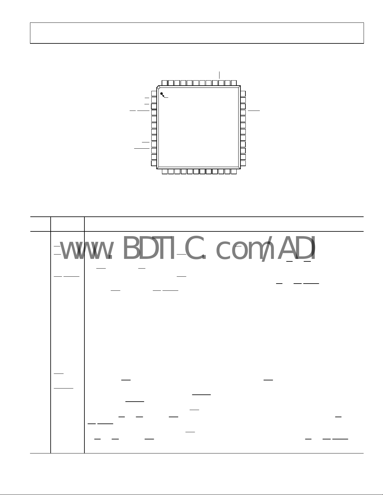
PIN CONFIGURATION AND FUNCTION DESCRIPTIONS
Table 4. Pin Function Descriptions
Pin
No. Mnemonic Description
1 RES1
Resolution Select 1. Logic input. RES1 in conjunction with RES0 allows the resolution of the AD2S1210 to be
programmed. Refer to the Configuration of AD2S1210 section.
2
3
Chip Select. Active low logic input. The device is enabled when CS is held low.
CS
Edge-Triggered Logic Input. When the SOE pin is high, this pin acts as a frame synchronization signal and output
RD
enable for the parallel data outputs, DB15 to DB0. The output buffer is enabled when CS
the SOE pin is low, the RD pin should be held high.
4
/FSYNC Edge-Triggered Logic Input. When the SOE pin is high, this pin acts as a frame synchronization signal and input
WR
enable for the parallel data inputs, DB7 to DB0. The input buffer is enabled when CS
When the SOE
5, 19 DGND
Digital Ground. These pins are ground reference points for digital circuitry on the AD2S1210. Refer all digital input
signals to this DGND voltage. Both of these pins can be connected to the AGND plane of a system. The DGND and
AGND voltages should ideally be at the same potential and must not be more than 0.3 V apart, even on a transient basis.
6 DVDD
Digital Supply Voltage, 4.75 V to 5.25 V. This is the supply voltage for all digital circuitry on the AD2S1210. The AV
voltages ideally should be at the same potential and must not be more than 0.3 V apart, even on a transient basis.
7 CLKIN
Clock Input. A crystal or oscillator can be used at the CLKIN and XTALOUT pins to supply the required clock frequency of
the AD2S1210. Alternatively, a single-ended clock can be applied to the CLKIN pin. The input frequency of the AD2S1210 is
specified from 6.144 MHz to 10.24 MHz.
8 XTALOUT
Crystal Output. When using a crystal or oscillator to supply the clock frequency to the AD2S1210, apply the crystal
across the CLKIN and XTALOUT pins. When using a single-ended clock source, the XTALOUT pin should be
considered a no connect pin.
9
Serial Output Enable. Logic input. This pin enables either the parallel or serial interface. The serial interface is selected
SOE
by holding the SOE
10
SAMPLE
Sample Result. Logic input. Data is transferred from the position and velocity integrators to the position and velocity
registers, after a high-to-low transition on the SAMPLE
transition on the SAMPLE
11 DB15/SDO
Data Bit 15/Serial Data Output Bus. When the SOE
controlled by CS
WR/FSYNC. The bits are clocked out on the rising edge of SCLK.
12 DB14/SDI
Data Bit 14/Serial Data Input Bus. When the SOE
and RD. When the SOE pin is low, this pin acts as SDI, the serial data input bus controlled by CS and WR/FSYNC. The
by CS
bits are clocked in on the falling edge of SCLK.
AD2S1210
TOP VIEW
(Not to Scale)
16
18
17
DB9
DB10
DD
SINLO41SIN40AGND39EXC38EXC37A0
42
20
19
DB821DB722DB623DB524DB4
DRIVE
DGND
V
36
35
34
33
32
31
30
29
28
27
26
25
A1
DOS
LOT
RESET
DIR
NM
B
A
DB0
DB1
DB2
DB3
07467-002
RES1
CS
RD
R/FSYNC
DGND
DV
CLKIN
XTALOUT
SOE
SAMPLE
DB15/SDO
DB14/SDI
RES047REFOU
REFBYP45COS44COSLO43AV
48
46
1
PIN 1
2
3
4
5
6
DD
7
8
9
10
11
12
13
14
15
DB11
DB12
DB13/SCLK
Figure 2. Pin Configuration
and RD are held low. When
and WR/FSYNC are held low.
pin is low, the WR/FSYNC pin acts as a frame synchronization signal and enable for the serial data bus.
and DVDD
DD
pin low, and the parallel interface is selected by holding the SOE pin high.
signal. The fault register is also updated after a high-to-low
signal.
pin is high, this pin acts as DB15, a three-state data output pin
and RD. When the SOE pin is low, this pin acts as SDO, the serial data output bus controlled by CS and
pin is high, this pin acts as DB14, a three-state data output pin controlled
Rev. 0 | Page 9 of 36
AD2S1210
www.BDTIC.com/ADI
Pin
No. Mnemonic Description
13 DB13/SCLK
14 to
17
18 V
20 DB8
21 to
28
29 A
30 B
31 NM
32 DIR
33
34 LOT
35 DOS
36 A1
37 A0
38 EXC
39
40 AGND
41 SIN Positive Analog Input of Differential SIN/SINLO Pair. The input range is 2.3 V p-p to 4.0 V p-p.
42 SINLO Negative Analog Input of Differential SIN/SINLO Pair. The input range is 2.3 V p-p to 4.0 V p-p.
43 AVDD
44 COSLO Negative Analog Input of Differential COS/COSLO Pair. The input range is 2.3 V p-p to 4.0 V p-p.
45 COS Positive Analog Input of Differential COS/COSLO Pair. The input range is 2.3 V p-p to 4.0 V p-p.
46 REFBYP Reference Bypass. Connect reference decoupling capacitors at this pin. Typical recommended values are 10 μF and 0.01 μF.
47 REFOUT Voltage Reference Output.
48 RES0
DB12 to
DB9
DRIVE
DB7 to DB0
Reset. Logic input. The AD2S1210 requires an external reset signal to hold the RESET input low until VDD is within the
RESET
Excitation Frequency Complement. Analog output. An on-board oscillator provides the sinusoidal excitation signal
EXC
Data Bit 13/Serial Clock. In parallel mode, this pin acts as DB13, a three-state data output pin controlled by CS
serial mode, this pin acts as the serial clock input.
Data Bit 12 to Data Bit 9. Three-state data output pins controlled by CS and RD.
Logic Power Supply Input. The voltage supplied at this pin determines at what voltage the interface operates.
Decouple this pin to DGND. The voltage range on this pin is 2.3 V to 5.25 V and may be different to the voltage range
and DVDD but should never exceed either by more than 0.3 V.
at AV
DD
Data Bit 8. Three-state data output pin controlled by CS
Data Bit 7 to Data Bit 0. Three-state data input/output pins controlled by CS
Incremental Encoder Emulation Output A. Logic output. This output is free running and is valid if the resolver format
input signals applied to the converter are valid.
Incremental Encoder Emulation Output B. Logic output. This output is free running and is valid if the resolver format
input signals applied to the converter are valid.
North Marker Incremental Encoder Emulation Output. Logic output. This output is free running and is valid if the
resolver format input signals applied to the converter are valid.
Direction. Logic output. This output is used in conjunction with the incremental encoder emulation outputs. The DIR
output indicates the direction of the input rotation and is high for increasing angular rotation.
specified operating range of 4.75 V to 5.25 V.
Loss of Tracking. Logic output. LOT is indicated by a logic low on the LOT pin and is not latched. Refer to the Loss of
Position Tracking Detection section.
Degradation of Signal. Logic output. Degradation of signal (DOS) is detected when either resolver input (sine or cosine)
exceeds the specified DOS sine/cosine threshold or when an amplitude mismatch occurs between the sine and
cosine input voltages. DOS is indicated by a logic low on the DOS pin. Refer to the Signal Degradation Detection
section.
Mode Select 1. Logic input. A1 in conjunction with A0 allows the mode of the AD2S1210 to be selected. Refer to the
Configuration of AD2S1210 section.
Mode Select 0. Logic input. A0 in conjunction with A1 allows the mode of the AD2S1210 to be selected. Refer to the
Configuration of AD2S1210 section.
Excitation Frequency. Analog output. An on-board oscillator provides the sinusoidal excitation signal (EXC) and its
complement signal (EXC
frequency register.
(EXC) and its complement signal (EXC
excitation frequency register.
Analog Ground. This pin is the ground reference points for analog circuitry on the AD2S1210. Refer all analog input
signals and any external reference signal to this AGND voltage. Connect the AGND pin to the AGND plane of a
system. The AGND and DGND voltages should ideally be at the same potential and must not be more than 0.3 V
apart, even on a transient basis.
Analog Supply Voltage, 4.75 V to 5.25 V. This pin is the supply voltage for all analog circuitry on the AD2S1210. The
and DVDD voltages ideally should be at the same potential and must not be more than 0.3 V apart, even on a
AV
DD
transient basis.
Resolution Select 0. Logic input. RES0 in conjunction with RES1 allows the resolution of the AD2S1210 to be
programmed. Refer to the Configuration of AD2S1210 section.
) to the resolver. The frequency of this reference signal is programmable via the excitation
) to the resolver. The frequency of this reference signal is programmable via the
and RD.
, RD, and WR/FSYNC.
and RD. In
Rev. 0 | Page 10 of 36
AD2S1210
www.BDTIC.com/ADI
TYPICAL PERFORMANCE CHARACTERISTICS
TA = 25°C, AVDD = DVDD = V
400
350
300
250
200
150
HITS P ER CODE
100
50
0
8178
8179
8180
8181
8182
8183
8184
8185
8186
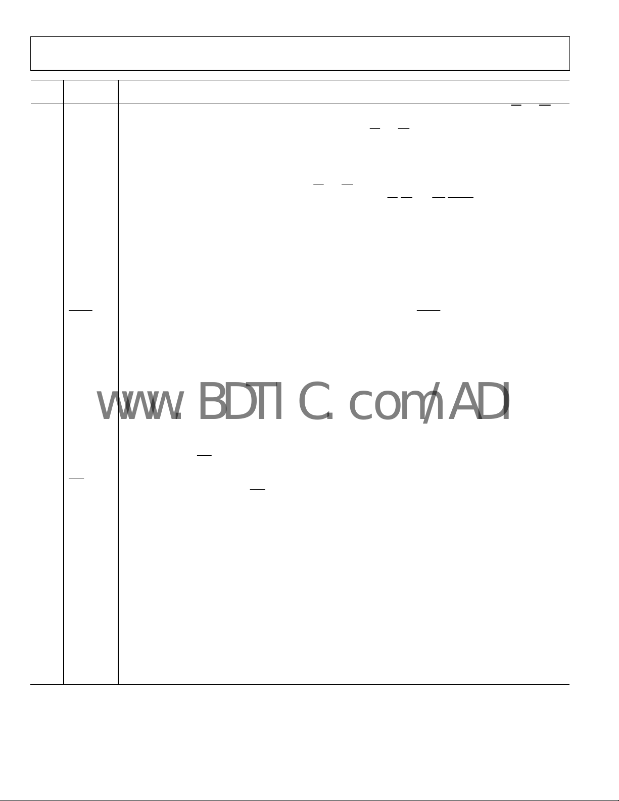
Figure 3. Typical 16-Bit Angular Accuracy Histogram Of Codes, 512 Samples
500
450
400
350
300
250
200
HITS PER CODE
150
100
50
0
8178
8179
8180
8181
8182
8183
8184
8185
8186
Figure 4. Typical 14-Bit Angular Accuracy Histogram of Codes, 512 Samples,
600
500
400
300
HITS PER CODE
200
100
0
2045 2046 2047 2048 2049
Figure 5. Typical 14-Bit Angular Accuracy Histogram of Codes, 512 Samples,
= 5 V, SIN/SINLO = 3.15 V p-p, COS/COSLO = 3.15 V p-p, CLKIN = 8.192 MHz , unless otherwise noted.
DRIVE
200
180
160
140
120
100
80
HITS PER CODE
60
40
20
0
8188
8189
8190
8191
8192
8193
8194
8195
8196
8197
8198
8199
8200
8201
8202
8203
8204
8205
8187
CODE
8206
07467-003
8178
8179
8180
8181
8182
8183
8184
8185
8186
8188
8189
8190
8191
8192
8193
8194
8195
8187
CODE
8196
Figure 6. Typical 12-Bit Angular Accuracy Histogram of Codes, 512 Samples,
Hysteresis Disabled
600
500
400
300
HITS PER CODE
200
100
0
8187
8188
8189
8190
8191
8192
8193
8194
8195
8196
8197
8198
8199
8200
8201
8202
8203
8204
8205
8206
CODE
07467-004
Figure 7. Typical 12-Bit Angular Accuracy Histogram of Codes, 512 Samples,
510 511 512 513 514
CODES
Hysteresis Enabled
Hysteresis Disabled
CODES
07467-005
HITS PER CODE
60
50
40
30
20
10
0
8178
8179
8180
8181
8182
8183
8184
8185
8186
8188
8189
8190
8191
8192
8193
8194
8195
8196
8187
CODE
8197
Figure 8. Typical 10-Bit Angular Accuracy Histogram of Codes, 512 Samples,
Hysteresis Enabled
Hysteresis Disabled
8197
8198
8199
8200
8201
8202
8203
8204
8205
8206
07467-006
07467-017
8198
8199
8200
8201
8202
8203
8204
8205
8206
07467-018
Rev. 0 | Page 11 of 36

AD2S1210
www.BDTIC.com/ADI
600
500
400
300
HITS PER CODE
200
100
0
126 127 128 129 130
CODES
07467-038
Figure 9. Typical 10-Bit Angular Accuracy Histogram of Codes, 512 Samples,
Hysteresis Enabled
20
18
16
14
12
10
8
ANGLE (Deg rees)
6
4
2
0
0 4 8 1216 202428323640
TIME (ms)
07467-010
Figure 10. Typical 16-Bit 10° Step Response
20
18
16
14
12
10
8
ANGLE (Degrees)
6
4
2
0
0 0.50 1.00 1.50 2.00 2.50 3.00 3.50 4.00 4.50 5.00
TIME (ms)
Figure 12. Typical 12-Bit 10° Step Response
20
18
16
14
12
10
8
ANGLE (Deg rees)
6
4
2
0
0 0.25 0.50 0.75 1.00 1.25 1.50 1.75 2.00 2.25 2.50
TIME (ms)
Figure 13. Typical 10-Bit 10° Step Response
07467-008
07467-007
20
18
16
14
12
10
8
ANGLE (Degrees)
6
4
2
0
01 2345678910
TIME (ms)
Figure 11. Typical 14-Bit 10° Step Response
07467-009
Rev. 0 | Page 12 of 36
250
225
200
175
150
125
100
ANGLE (Deg rees)
75
50
25
0
0 8 16 24 32 40 48 56 64 72 80
TIME (ms)
Figure 14. Typical 16-Bit 179° Step Response
07467-014

AD2S1210
www.BDTIC.com/ADI
250
225
200
175
150
125
100
ANGLE (Degrees)
75
50
25
0
0 2 4 6 8 10 12 14 16 18 20
TIME (ms)
Figure 15. Typical 14-Bit 179° Step Response
07467-013
5
0
–5
–10
–15
–20
–25
MAGNITUDE (dB)
–30
–35
–40
–45
1 10 100 1k 10k 100k
14-BIT
16-BIT
FREQUENCY (Hz)
10-BIT
12-BIT
Figure 18. Typical System Magnitude Response
07467-015
250
225
200
175
150
125
100
ANGLE (Degrees)
75
50
25
0
012345678910
TIME (ms)
Figure 16. Typical 12-Bit 179° Step Response
250
225
200
175
150
125
100
ANGLE (Deg rees)
75
50
25
0
012345
TIME (ms)
Figure 17. Typical 10-Bit 179° Step Response
0
–20
–40
–60
–80
–100
–120
PHASE (dB)
–140
–160
–180
–200
1 10 100 1k 10k 100k
07467-012
14-BIT 12-BIT
16-BIT
FREQUENCY (Hz)
10-BIT
07467-016
Figure 19. Typical System Phase Response
10
9
8
7
6
5
4
3
TRACKING ERROR ( Degrees)
2
1
0
07467-011
0 500 1000 1500 2000 2500
ACCELERATIO N (rps
2
)
07467-022
Figure 20. Typical 16-Bit Tracking Error vs. Acceleration
Rev. 0 | Page 13 of 36

AD2S1210
www.BDTIC.com/ADI
10
9
8
7
6
5
4
3
TRACKING ERROR ( Degrees)
2
1
0
0 5000 10000 15000 20000 25000 30000 35000 40000 45000
ACCELERATIO N (rps
2
)
Figure 21. Typical 14-Bit Tracking Error vs. Acceleration
10
9
8
7
6
5
4
3
TRACKING ERROR ( Degrees)
2
1
0
0 20000 60000 100000 140000 180000
ACCELERATIO N (rps
2
)
Figure 22. Typical 12-Bit Tracking Error vs. Acceleration
07467-021
07467-020
10
9
8
7
6
5
4
3
TRACKING ERROR ( Degrees)
2
1
0
0 200000 400000 600000 800000 1000000
ACCELERATIO N (rps
2
)
Figure 23. Typical 10-Bit Tracking Error vs. Acceleration
07467-019
Rev. 0 | Page 14 of 36
AD2S1210
V
V
V
V
)
θ
ω
www.BDTIC.com/ADI
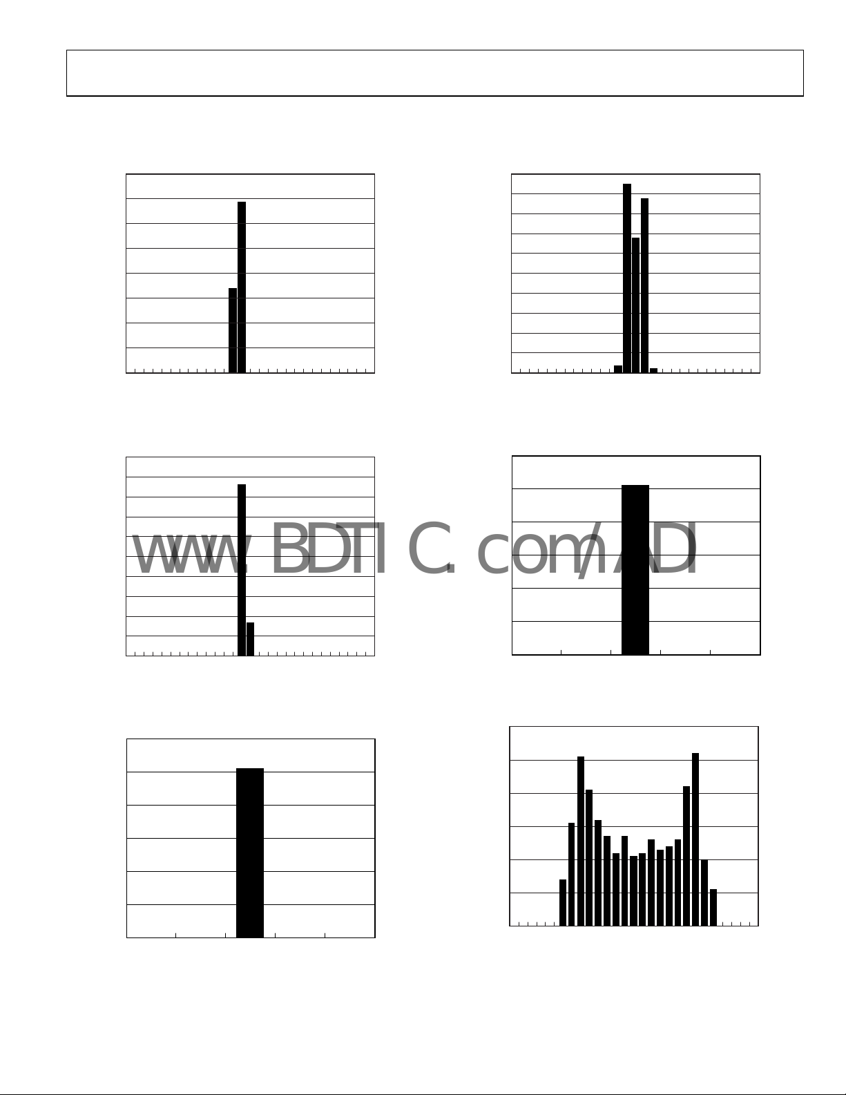
RESOLVER FORMAT SIGNALS
=
× sin(ωt)
r
p
R1
θ
R2
S1 S3
= Vs × sin(ωt) × sin(θ)
V
b
(A) CLASSICAL RESOLVER
S2
Va = Vs × sin(ωt) × cos(θ)
S4
Figure 24. Classical Resolver vs. Variable Reluctance Resolver
A resolver is a rotating transformer, typically with a primary
winding on the rotor and two secondary windings on the stator.
In the case of a variable reluctance resolver, there are no windings on the rotor, as shown in Figure 24. The primary winding
is on the stator as well as the secondary windings, but the saliency
in the rotor design provides the sinusoidal variation in the
secondary coupling with the angular position. Either way, the
resolver output voltages (S3 − S1, S2 − S4) have the same
equations, as shown in Equation 1.
0
tESS
0
(1)
θω
cossin42
×=−
sinsin13
×=−
tESS
where:
θ is the shaft angle.
Sinωt is the rotor excitation frequency.
E
is the rotor excitation amplitude.
0
R1
R2
=
× sin(ωt)
r
p
S2
Va = Vs × sin(ωt) × cos(θ
θ
S1 S3
= Vs × sin(ωt) × sin(θ)
V
b
(B) VARIABLE RELUCTANCE RESOLVER
S4
07467-023
The stator windings are displaced mechanically by 90° (see
Figure 24). The primary winding is excited with an ac reference.
The amplitude of subsequent coupling onto the stator secondary
windings is a function of the position of the rotor (shaft) relative to
the stator. The resolver, therefore, produces two output voltages
(S3 − S1, S2 − S4) modulated by the sine and cosine of shaft
angle. Resolver format signals refer to the signals derived from
the output of a resolver, as shown in Equation 1. Figure 25
illustrates the output format.
S2 – S4
(cos)
S3 – S1
(sin)
R2 – R4
(REF)
0°
90° 180°
θ
Figure 25. Electrical Resolver Representation
270° 360°
07467-024
Rev. 0 | Page 15 of 36

AD2S1210
φθω
φθω
φθφθω
φθφ
θ
φθφ
θ
××=
www.BDTIC.com/ADI
THEORY OF OPERATION
RESOLVER TO DIGITAL CONVERSION
The AD2S1210 operates on a Type II tracking closed-loop
principle. The output continually tracks the position of the
resolver without the need for external conversion and wait
states. As the resolver moves through a position equivalent
to the least significant bit weighting, the output is updated by
one LSB.
The converter tracks the shaft angle θ by producing an output
angle ϕ that is fed back and compared to the input angle θ, and
the resulting error between the two is driven towards 0 when
the converter is correctly tracking the input angle. To measure
the error, S3 − S1 is multiplied by cosϕ and S2 − S4 is multiplied by
sinϕ to give
cossinsin0×tE (for S3 − S1)
sincossin0×tE (for S2 − S4)
The difference is taken, giving
0
This signal is demodulated using the internally generated
synthetic reference, yielding
0
Equation 3 is equivalent to E
equal to E
angular error.
The value E
of the rotor and the digital angle output of the converter.
A phase-sensitive demodulator, some integrators, and a compensation filter form a closed-loop system that seeks to null the error
signal. When this is accomplished, ϕ equals the Resolver Angle θ
within the rated accuracy of the converter. A Type II tracking
loop is used so that constant velocity inputs can be tracked
without inherent error.
(θ − ϕ) for small values of θ − ϕ, where θ − ϕ =
0
−E (3)
(θ − ϕ) is the difference between the angular error
0
−×tE (2)
)sincoscos(sin
sin(θ − ϕ), which is approximately
0
)sincoscos(sinsin
FAULT DETECTION CIRCUIT
The AD2S1210 fault detection circuit can sense loss of resolver
signals, out-of-range input signals, input signal mismatch, or
loss of position tracking; however, in the event of a fault, the
position indicated by the AD2S1210 may differ significantly
from the actual shaft position of the resolver.
Monitor Signal
The AD2S1210 generates a monitor signal by comparing the
angle in the position register to the incoming sine and cosine
signals from the resolver. The monitor signal is created in a
similar fashion to the error signal described in the Resolver to
Digital Conversion section. The incoming signals, sinθ and
cosθ, are multiplied by the sin and cos of the output angle,
respectively, and then added together.
AAMonitor (4)
where:
A1 is the amplitude of the incoming sine signal (A1 × sinθ).
A2 is the amplitude of the incoming cosine signal (A2 × cosθ).
θ is the resolver angle.
ϕ is the angle stored in the position register.
Note that Equation 4 is shown after demodulation, with the
Carrier Signal sinωt removed. Also, note that for matched input
signal (that is, a no fault condition), A1 = A2.
When A1 = A2 and the converter is tracking (θ = ϕ), the
monitor signal output has a constant magnitude of A1 (Monitor
= A1 × (sin
angle. When A1 ≠ A2, the monitor signal magnitude varies
between A1 and A2 at twice the rate of shaft rotation. The
monitor signal is used as described in the following sections to
detect degradation or loss of input signals.
2
θ + cos2 θ) = A1), which is independent of shaft
Loss of Signal Detection
The AD2S1210 indicates that a loss of signal (LOS) has
occurred for four separate conditions.
• When either resolver input (sine or cosine) falls below the
specified LOS sine/cosine threshold. This threshold is
defined by the user and is set by writing to the internal
register, Address 0x88 (see the Register Map section).
• When any of the resolver input pins (SIN, SINLO, COS, or
COSLO) are disconnected from the sensor.
• When any of the resolver input pins (SIN, SINLO, COS, or
COSLO) are clipping the power rail or ground rail of the
AD2S1210. Refer to the Sine/Cosine Input Clipping section.
• When a configuration parity error has occurred. Refer to
the Configuration Parity Error section.
A loss of signal is caused if either of the stator windings of the
resolver (sine or cosine) are open circuit or have a number of
shorted turns. LOS is indicated by both the DOS and LOT pins
latching as logic low outputs. The DOS and LOT pins are reset
to a no fault state when the user enters configuration mode and
reads the fault register. The LOS condition has priority over
both the DOS and LOT conditions, as shown in Table 6. To
determine the cause of the LOS fault detection, the user must
read the fault register, Address 0xFF (see the Register Map
section).
When a loss of signal is detected due to the resolver inputs (sine
or cosine) falling below the specified LOS sine/cosine threshold,
the electrical angle through which the resolver may rotate before
the LOS can be detected by the AD2S1210 is referred to as the
LOS angular latency. This is defined by the specified LOS sine/
cosine threshold set by the user and the maximum amplitude of
the input signals being applied to the AD2S1210. The worst-case
angular latency can be calculated as follows:
coscos2sinsin1 ××+
Rev. 0 | Page 16 of 36

AD2S1210
www.BDTIC.com/ADI
Angular Latency =
×
The preceding equation is based on the worst-case angular
error, which can be seen by the AD2S1210 before an LOS fault
is indicated. This occurs if one of the resolver input signals,
either sine or cosine, is lost while the remaining signal is at its
peak amplitude, for example, if the sine input is lost while the
input angle is 90°. The worst-case angular latency is twice the
worst-case angular error.
⎢
⎢
⎣
⎡
Arc
cos2 (5)
thresholdLOS
/max
amplitudecosinesine
⎤
⎥
⎥
⎦
Signal Degradation Detection
The AD2S1210 indicates that a degradation of signal (DOS) has
occurred for two separate conditions.
• When either resolver input (sine or cosine) exceeds the
specified DOS sine/cosine threshold. This threshold is
defined by the user and is set by writing to the internal
register, Address 0x89 (see the Register Map section).
• When the amplitudes of the input signals, sine and cosine,
mismatch by more than the specified DOS sine/cosine
mismatch threshold. This threshold is defined by the user
and is set by writing to the internal register, Address 0x8A
(see the Register Map section). The AD2S1210 continuously
stores the minimum and maximum magnitude of the monitor signal in internal registers. The difference between the
minimum and maximum is calculated to determine if a
DOS mismatch has occurred. The initial values for the
minimum and maximum internal registers must be defined
by the user, at Address 0x8C and Address 0x8B, respectively
(see the Register Map section).
DOS is indicated by a logic low on the DOS pin. When DOS is
indicated, the output is latched low until the user enters configuration mode and reads the fault register. The DOS condition has
priority over the LOT condition, as shown in Table 6. To determine the cause of the DOS fault detection, the user must read
the fault register, Address 0xFF (see the Register Map section).
Time Latency for LOS and DOS Detection
Note that the monitor signal is generated on the active edge of
the internal AD2S1210 clock. The internal clock is generated
by dividing the externally applied CLKIN frequency by 2; for
example, when using a CLKIN frequency of 8.192 MHz the
internal AD2S1210 clock is 4.096 MHz. The AD2S1210 continuously stores the minimum and maximum magnitude of the
monitor signal in internal registers. The values stored in these
internal registers are compared to the LOS and DOS thresholds
configured by the user at set intervals. This interval, known as
the window counter period, is dependent on the excitation
frequency configured by the user. It is set to ensure that two
window counter periods include at least one full period of the
excitation frequency applied to the resolver. The window
counter period is defined in terms of internal clock cycles. The
window counter periods for the range of excitation frequencies
on the AD2S1210 are outlined in Table 5.
Table 5. Window Counter Period vs. Excitation Frequency
Range, CLKIN = 8.192 MHz
Number of
Excitation Frequency
Range
2 kHz ≤ Exc Freq < 4 kHz 1065 260
4 kHz ≤ Exc Freq < 8 kHz 554 135.25
8 kHz ≤ Exc Freq ≤ 20 kHz 256 62.5
1
CLKIN = 8.192 MHz. The window counter period scales with clock frequency
and can be calculated by multiplying the number of internal clock cycles by
the period of the internal clock frequency, that is, CLKIN/2.
The AD2S1210 detects an LOS or DOS due to the resolver inputs
(sine or cosine) falling below or exceeding the LOS and DOS
thresholds within two window counter periods. For example,
with an excitation frequency of 10 kHz, a fault is detected within
125 μs. A persistent fault is detected within one window counter
period of the reading and clearing the fault register.
Note that the time latency to detect the occurrence of a DOS
mismatch fault is dependent on the speed of rotation of the
resolver. The worst-case time latency to detect a DOS mismatch
fault is the time required for one full rotation of the resolver.
Internal Clock
Cycles
Window
Counter Period
1
(μs)
Loss of Position Tracking Detection
The AD2S1210 indicates that a loss of tracking (LOT) has
occurred when
• The internal error signal of the AD2S1210 has exceeded
the specified angular threshold. This threshold is defined
by the user and is set by writing to the internal register,
Address 0x8D (see the Register Map section).
• The input signal exceeds the maximum tracking rate. The
maximum tracking rate depends on the resolution defined
by the user and the CLKIN frequency.
LOT is indicated by a logic low on the LOT pin and is not latched.
LOT has hysteresis and is not cleared until the internal error
signal is less than the value defined in the LOT low threshold
register, Address 0x8E (see the Register Map section).
When the maximum tracking rate is exceeded, LOT is cleared
only if the velocity is less than the maximum tracking rate and
the internal error signal is less than the value defined in the LOT
low threshold register. LOT can be indicated for step changes in
RESET
position (such as after a
It is also useful as a built-in test to indicate that the tracking
converter is functioning properly. The LOT condition has lower
priority than both the DOS and LOS conditions, as shown in
Table 6. The LOT and DOS conditions cannot be indicated using
the LOT and DOS pins at the same time. However, both conditions are indicated separately in the fault register. To determine
the cause of the LOT fault detection, the user must read the fault
register, Address 0xFF (see the Register Map section).
signal is applied to the AD2S1210).
Rev. 0 | Page 17 of 36

AD2S1210
www.BDTIC.com/ADI
Table 6. Fault Detection Decoding
Order of
Condition DOS Pin LOT Pin
Loss of Signal (LOS) 0 0 1
Degradation of Signal (DOS) 0 1 2
Loss of Tracking (LOT) 1 0 3
No Fault 1 1 N/A
Priority
Sine/Cosine Input Clipping
The AD2S1210 indicates that a clipping error has occurred if
any of the resolver input pins (SIN, SINLO, COS, or COSLO)
are clipping the power rail or ground rail of the AD2S1210. The
clipping fault is indicated if the input amplitudes are less than
0.15 V or greater then AV
Sine/cosine input clipping error is indicated by both the DOS and
LOT pins latching as logic low outputs. Sine/cosine input clipping
error is also indicated by Bit D7 of the fault register being set high.
The DOS and LOT pins are reset to a no fault state when the
user enters configuration mode and reads the fault register.
− 0.2 V for more than 4 μs.
DD
Configuration Parity Error
The AD2S1210 includes a number of user programmable registers
that allow the user to configure the part. Each read/write register
on the AD2S1210 is programmed with seven bits of information by the user. The 8
the event that the data within these registers becomes corrupted,
the AD2S1210 indicates that a configuration parity error has
occurred. Configuration parity error is indicated by both the DOS
and LOT pins latching as logic low outputs. Configuration parity
error is also indicated by Bit D0 of the fault register being set
high. In the event that a parity error occurs, it is recommended
that the user reset the part using the
th
bit is reserved as a parity error bit. In
RESET
pin.
Phase Lock Error
The AD2S1210 indicates that a phase lock error has occurred if
the difference between the phase of the excitation frequency
and the phase of the sine and cosine signals exceeds the specified
phase lock range. Phase lock error is indicated by a logic low on
the LOT pin and is not latched. Phase lock error is also indicated
by Bit D1 of the fault register being set high.
ON-BOARD PROGRAMMABLE SINUSOIDAL OSCILLATOR
An on-board oscillator provides the sinusoidal excitation signal
EXC
(EXC) to the resolver as well as its complemented signal (
The frequency of this reference signal is programmable to a
number of standard frequencies between 2 kHz and 20 kHz.
The amplitude of this signal is 3.6 V p-p and is centered on 2.5 V.
The reference excitation output of the AD2S1210 needs an
external buffer amplifier to provide gain and the additional
current to drive a resolver.
).
The AD2S1210 also provides an internal synthetic reference
signal that is phase locked to its sine and cosine inputs. Phase
errors between the resolver primary and secondary windings
can degrade the accuracy of the RDC and are compensated by
this synchronous reference signal. This also compensates the
phase shifts due to temperature and cabling and eliminates the
need of an external preset phase compensation circuit.
SYNTHETIC REFERENCE GENERATION
When a resolver undergoes a high rotation rate, the RDC tends
to act as an electric motor and produces speed voltages, along
with the ideal sine and cosine outputs. These speed voltages are
in quadrature to the main signal waveform. Moreover, nonzero
resistance in the resolver windings causes a nonzero phase shift
between the reference input and the sine and cosine outputs.
The combination of speed voltages and phase shift causes a tracking error in the RDC that is approximated by
ShiftPhaseError ×=
To compensate for the described phase error between the resolver
reference excitation and the sine/cosine signals, an internal
synthetic reference signal is generated in phase with the reference frequency carrier. The synthetic reference is derived using
the internally filtered sine and cosine signals. It is generated
by determining the zero crossing of either the sine or cosine
(whichever signal is larger, to improve phase accuracy) and
evaluating the phase of the resolver reference excitation. The
synthetic reference reduces the phase shift between the reference and sine/cosine inputs to less than 10°, and operates for
phase shifts of ±44°. If additional phase lock range is required,
Bit D5 in the control register can be set to zero to expand the
phase lock range to 360° (see the Control Register section).
RateRotation
FrequencyReference
(6)
CONNECTING THE CONVERTER
Ground is connected to the AGND and DGND pins (see
Figure 26). A positive power supply (V
connected to the AV
decoupling capacitors being 10 nF and 4.7 μF. These capacitors
are then placed as close to the device pins as possible and are
connected to both AV
to the supply voltage of the microprocessor. The voltage applied
to the V
interfaces. V
for the V
Typical values for the oscillator decoupling capacitors are 20 pF,
whereas typical values for the reference decoupling capacitors are
10 nF and 10 μF.
input controls the voltage of the parallel and serial
DRIVE
DRIVE
decoupling capacitors are 10 nF and 4.7 μF.
DRIVE
and DVDD pins, with typical values for the
DD
and DVDD. The V
DD
can be set to 5 V, 3 V, or 2.5 V. Typical values
) of 5 V dc ± 5% is
DD
pin is connected
DRIVE
Rev. 0 | Page 18 of 36

AD2S1210
×
×+×−
=
www.BDTIC.com/ADI
4.7µF 10n F
10nF 10µF
5V
20pF 20pF
4.7µF10nF
8.192
MHZ
5V
48 47
1
2
3
4
5
DGND
6
DV
DD
7
CLKIN
8
XTALOUT
9
10
11
12
13
S2 R2
S4 S3 S1 R1
46
45
44
43
COS
COSLO
REFBYP
REFOUT
AD2S1210
14 15
161718
V
DRIVE
10nF
42
41
DD
AV
SINLO
DRIVE
V
DGND
19
202122 23 24
BUFFER
CIRCUIT
40
SIN
AGND
4.7µF
39
EXC38EXC
BUFFER
CIRCUIT
37
36
35
34
33
32
31
30
29
28
27
26
25
07467-025
Figure 26. Connecting the AD2S1210 to a Resolver
In this recommended configuration, the converter introduces a
/2 offset in the SIN, SINLO, COS, and COSLO signal outputs
V
REF
from the resolver. The sine and cosine signals can each be
connected to a different potential relative to ground if the sine
and cosine signals adhere to the recommended specifications.
EXC
Note that because the EXC and
outputs are differential,
there is an inherent gain of 2×.
Figure 27 shows a suggested buffer circuit. Capacitor C1 may be
used in parallel with Resistor R2 to filter out any noise that may
EXC
exist on the EXC and
outputs. Care should be taken when
selecting the cutoff frequency of this filter to ensure that phase
shifts of the carrier caused by the filter do not exceed the phase
lock range of the AD2S1210.
The gain of the circuit is
))1/(1()/( ωC1R2R1R2GainCarrier
(7)
and
OUT
⎛
VV
⎜
⎝
R2
⎛
1 (8)
+×=
⎜
R1
⎝
R2
⎞
⎞
⎛
⎞
⎟
⎟
⎠
⎠
×
−
⎟
⎜
⎠
⎝
1
⎛
⎜
1
⎝
⎞
V
⎟
C1R2R1
INREF
××+
ω
⎠
where:
ω is the radian frequency of the applied signal.
, a dc voltage, is set so that V
V
REF
is always a positive value,
OUT
eliminating the need for a negative supply.
C1
EXC/EXC
(V
R2
12V
R1
)
IN
(V
)
AD8662
REF
5V
12V
V
OUT
04767-026
Figure 27. Buffer Circuit
A separate screened twisted pair cable is recommended for the
analog input pins, SIN, SINLO, COS, and COSLO. The screens
should terminate to either REFOUT or AGND.
Rev. 0 | Page 19 of 36

AD2S1210
(
)
www.BDTIC.com/ADI
CONFIGURATION OF AD2S1210
MODES OF OPERATION
The AD2S1210 has two modes of operation: configuration mode
and normal mode. The configuration mode is used to program
the registers that set the excitation frequency, the resolution,
and the fault detection thresholds of the AD2S1210. Configuration
mode is also used to read back the information in the fault register.
The data in the position and velocity registers can also be read
back while in configuration mode. The AD2S1210 can be operated
entirely in configuration mode or, when the initial configuration is
completed, the part can be taken out of configuration mode and
operated in normal mode. When operating in normal mode, the
data outputs can provide angular position or angular velocity
data. The A0 and A1 inputs are used to determine whether the
AD2S1210 is in configuration mode and to determine whether
the position or velocity data is supplied to the output pins, see
Tabl e 8.
Setting the Excitation Frequency
The excitation frequency of the AD2S1210 is set by writing a
frequency control word to the excitation frequency register,
Address 0x91 (see the Register Map section).
FrequencyExcitation
where FCW is the frequency control word and f
frequency of the AD2S1210.
The specified range of the excitation frequency is from 2 kHz to
20 kHz and can be set in increments of 250 Hz. To achieve the
angular accuracy specifications in Table 1, the excitation frequency
should be selected as outlined in Table 7.
Table 7. Recommended Excitation Frequency vs. Resolution
= 8.192 MHz)
(f
CLKIN
Typ ic al
Resolution
10 Bits 4100 Hz 10 kHz 20 kHz
12 Bits 1700 Hz 6 kHz 20 kHz
14 Bits 900 Hz 3 kHz 12 kHz
16 Bits 250 Hz 2 kHz 10 kHz
Bandwidth
=
×
15
2
Min Excitation
Frequency
fFCW
CLKIN
is the clock
CLKIN
Max Excitation
Frequency
Note that the recommended frequency range for each resolution
and bandwidth, as outlined in Table 7, are defined for a clock
frequency of 8.192 MHz. The recommended excitation frequency
range scales with the clock frequency of the AD2S1210. The
default excitation frequency of the AD2S1210 is 10 kHz when
operated with a clock frequency of 8.192 MHz.
A0, A1 Inputs
The AD2S1210 allows the user to read the angular position or
the angular velocity data directly from the parallel outputs or
through the serial interface. The required information can be
selected using the A0 and A1 inputs. These inputs should also
be used to put the part into configuration mode. The data from
the fault register and the remaining on-chip registers can be
accessed in configuration mode.
Table 8. Configuration Mode Settings
A0 A1 Result
0 0 Normal mode—position output
0 1 Normal mode—velocity output
1 0 Reserved
1 1 Configuration mode
RES0, RES1 Inputs
In normal mode, the resolution of the digital output is selected
using the RES0 and RES1 input pins. In configuration mode,
the resolution is selected by setting the RES0 and RES1 bits in
the control register. When switching between normal mode and
configuration mode, it is the responsibility of the user to ensure
that the resolution set in the control register matches the resolution
set by the RES0 and RES1 input pins. Failure to do so may result
in incorrect data on the outputs, caused by the differences
between the resolution settings.
Table 9. Resolution Settings
Resolution
RES0 RES1
0 0 10 21.1 4.88
0 1 12 5.3 0.488
1 0 14 1.3 0.03
1 1 16 0.3 0.004
1
CLKIN = 8.192 MHz. The velocity LSB size and maximum tracking rate scale
linearly with the CLKIN frequency.
(Bits)
Position LSB
(Arc min)
Velocity LSB
(rps)1
Rev. 0 | Page 20 of 36

AD2S1210
www.BDTIC.com/ADI
REGISTER MAP
Table 10. Register Map
Register
Register Name
Position 0x80 D15 to D8 Read only
0x81 D7 to D0 Read only
Velocity 0x82 D15 to D8 Read only
0x83 D7 to D0 Read only
LOS Threshold 0x88 D7 to D0 Read/write
DOS Overrange
Threshold
DOS Mismatch
Threshold
DOS Reset Max
Threshold
DOS Reset Min
Threshold
LOT High Threshold 0x8D D7 to D0 Read/write
LOT Low Threshold 0x8E D7 to D0 Read/write
Excitation Frequency 0x91 D7 to D0 Read/write
Control 0x92 D7 to D0 Read/write
Soft Reset 0xF0 D7 to D0 Write only
Fault 0xFF D7 to D0 Read only
Address
0x89 D7 to D0 Read/write
0x8A D7 to D0 Read/write
0x8B D7 to D0 Read/write
0x8C D7 to D0 Read/write
Register
Data
Read/Write
Register
POSITION REGISTER
Table 11. 16-Bit Register
Address Bit Read/Write
0x80 D15 to D8 Read only
0x81 D7 to D0 Read only
The position register contains a digital representation of the
angular position of the resolver input signals. The values are
stored in 16-bit binary format. The value in the position register
is updated following a falling edge on the
Note that with hysteresis enabled (see the Control Register
section), at lower resolutions, the LSBs of the 16-bit digital output
are set to zero. For example, at 10-bit resolution, Data Bit D15 to
Data Bit D6 provide valid data; D5 to D0 are set to zero. With
hysteresis disabled, the value stored in the position register is 16
bits regardless of resolution. At lower resolutions, the LSBs of
the 16-bit digital output can be ignored. For example, at 10-bit
resolution, Data Bit D15 to Data Bit D6 provide valid data; D5
to D0 can be ignored.
SAMPLE
input.
VELOCITY REGISTER
Table 12. 16-Bit Register
Address Bit Read/Write
0x82 D15 to D8 Read only
0x83 D7 to D0 Read only
The velocity register contains a digital representation of the angular
velocity of the resolver input signals. The value in the velocity
register is updated following a falling edge on the sample input.
The values are stored in 16-bit, twos complement format. The
maximum velocity that the AD2S1210 can track for each
resolution is specified in Table 1. For example, the maximum
tracking rate of the AD2S1210 at 16 bits resolution, with an
8.192 MHz input clock, is
results in 0x7FFF being stored in the velocity register; a velocity
of −125 rps results in 0x8000 being stored in the velocity register.
The value stored in the velocity register is 16 bits regardless of
resolution. At lower resolutions, the LSBs of the 16-bit digital
output should be ignored. For example, at 10-bit resolution,
Data Bit D15 to Data Bit D6 provide valid data; D5 to D0 should
be ignored. The maximum tracking rate of the AD2S1210 at
10-bit resolution with an 8.192 MHz input clock is
A velocity of +2500 rps results in 0x1FF being stored in Bit D15 to
Bit D6 of the velocity register; a velocity of −2500 rps results in
0x3FF being stored in Bit D15 to Bit D6 of the velocity register. In
this 10-bit example, the LSB size of the velocity output is 4.88 rps.
±125 rps. A velocity of +125 rps
±2500 rps.
LOS THRESHOLD REGISTER
Table 13. 8-Bit Register
Address Bit Read/Write
0x88 D7 to D0 Read/write
The LOS threshold register determines the loss of signal threshold
of the AD2S1210. The AD2S1210 allows the user to set the LOS
threshold to a value between 0 V and 4.82 V. The resolution of
the LOS threshold is seven bits, that is, 38 mV. Note that the MSB,
D7, should be set to 0. The default value of the LOS threshold
on power-up is 2.2 V.
DOS OVERRANGE THRESHOLD REGISTER
Table 14. 8-Bit Register
Address Bit Read/Write
0x89 D7 to D0 Read/write
The DOS overrange threshold register determines the degradation
of signal threshold of the AD2S1210. The AD2S1210 allows the
user to set the DOS overrange threshold to a value between 0 V
and 4.82 V. The resolution of the DOS overrange threshold is
seven bits, that is, 38 mV. Note that the MSB, D7, should be set to
0. The default value of the DOS overrange threshold on power-up
is 4.1 V.
DOS MISMATCH THRESHOLD REGISTER
Table 15. 8-Bit Register
Address Bit Read/Write
0x8A D7 to D0 Read/write
The DOS mismatch threshold register determines the signal
mismatch threshold of the AD2S1210. The AD2S1210 allows
the user to set the DOS mismatch threshold to a value between
0 V and 4.82 V. The resolution of the DOS mismatch threshold
is seven bits, that is, 38 mV. Note that the MSB, D7, should be
set to 0.The default value of the DOS mismatch threshold on
power-up is 380 mV.
Rev. 0 | Page 21 of 36

AD2S1210
(
)
(
)
www.BDTIC.com/ADI
DOS RESET MAXIMUM AND MINIMUM THRESHOLD REGISTERS
Table 16. 8-Bit Registers
Address Bit Read/Write
0x8B D7 to D0 Read/write
0x8C D7 to D0 Read/write
The AD2S1210 continuously stores the minimum and maximum
magnitude of the monitor signal in internal registers. The difference between the minimum and maximum is calculated to
determine if a DOS mismatch has occurred. The initial values
for the minimum and maximum internal registers must be
defined by the user. When the fault register is cleared, the
registers that store the maximum and minimum amplitudes of
the monitor signal are reset to the values stored in the DOS reset
maximum and minimum threshold registers. The resolution of
the DOS reset maximum and minimum thresholds is seven bits
each, that is, 38 mV. Note that the MSB, D7, should be set to
0.To ensure correct operation, it is recommended that the DOS
reset minimum threshold register be set to at least 1 LSB less
than the DOS overrange threshold, and the DOS reset maximum
threshold register be set to at least 1 LSB greater than the LOS
threshold register. The default value of the DOS reset minimum
threshold register and the DOS reset maximum threshold
register are 3.99 V and 2.28 V, respectively.
LOT HIGH THRESHOLD REGISTER
Table 17. 8-Bit Register
Address Bit Read/Write
0x8D D7 to D0 Read/write
The LOT high threshold register determines the loss of position
tracking threshold for the AD2S1210. The LOT high threshold
is a 7-bit word. Note that the MSB, D7, should be set to 0. The
range of the LOT high threshold, the LSB size, and the default
value of the LOT high threshold on power-up are dependent on
the resolution setting of the AD2S1210, and are outlined in
Table 19.
LOT LOW THRESHOLD REGISTER
Table 18. 8-Bit Register
Address Bit Read/Write
0x8E D7 to D0 Read/write
The LOT low threshold register determines the level of hysteresis
on the loss of position tracking fault detection. Loss of tracking
(LOT) occurs when the internal error signal of the AD2S1210
exceeds the LOT high threshold. LOT has hysteresis and is not
cleared until the internal error signal is less than the value defined
in the LOT low threshold register. The LOT low threshold is a
7-bit word. Note that the MSB, D7, should be set to 0. The range
of the LOT high threshold, the LSB size, and the default value of
the LOT high threshold on power-up are dependent on the resolution setting of the AD2S1210, and are outlined in Table 19.
Rev. 0 | Page 22 of 36
Table 19. LOT High/Low Threshold
LOT Low
Resolution
(Bits)
10 0 to 45 0.35 2.5 12.5
12 0 to 18 0.14 1.0 5.0
14 0 to 9 0.09 0.5 2.5
16 0 to 9 0.09 0.5 2.5
Range
(Degrees)
LSB Size
(Degrees)
Default
(Degrees)
LOT High
Default
(Degrees)
EXCITATION FREQUENCY REGISTER
Table 20. 8-Bit Register
Address Bit Read/Write
0x91 D7 to D0 Read/write
The excitation frequency register determines the frequency of
the excitation outputs of the AD2S1210. A 7-bit frequency control
word is written to the register to set the excitation frequency.
Note that the MSB, D7, should be set to 0.
FCW
= (9)
where FCW is the frequency control word and f
frequency of the AD2S1210. The specified range of the excitation
frequency is from 2 kHz to 20 kHz and can be set in increments
of 250 Hz. To ensure that the AD2S1210 is operated within the
specified frequency range, the frequency control word should
be a value between 0x4 and 0x50.
For example, if the user requires an excitation frequency of 5 kHz
and has an 8.192 MHz clock frequency, the code that needs to
be programmed is given by
=FCW (hexadecimal)
The default excitation frequency of the AD2S1210 on power-up
is 10 kHz.
FrequencyExcitation
f
CLKIN
15
2kHz5
×
MHz192.8
14
=
15
2×
is the clock
CLKIN
CONTROL REGISTER
Table 21. 8-Bit Register
Address Bit Read/Write
0x92 D7 to D0 Read/write
The control register is an 8-bit register that sets the AD2S1210
control modes. The default value of the control register on
power-up is 0x7E.
Table 22. Control Register Bit Descriptions
Bit Description
D7 Address/data bit
D6 Reserved; set to 1
D5 Phase lock range
0 = 360°, 1 = ±44°
D4 0 = disable hysteresis, 1 = enable hysteresis
D3 Set Encoder Resolution EnRES1
D2 Set Encoder Resolution EnRES0
D1 Set Resolution RES1
D0 Set Resolution RES0

AD2S1210
www.BDTIC.com/ADI
Address/Data Bit
The MSB of each 8-bit word written to the AD2S1210 indicates
whether the 8-bit word is a register address or data. The MSB
(D7) of each register address defined on the AD2S1210 is high.
The MSB of each data word written to the AD2S1210 is low.
Note that when a data word is written to the AD2S1210, the
MSB is internally reconfigured as a parity bit. When reading
data from any of the read/write registers (see Table 10), the
parity of Bit D6 to Bit D0 is recalculated and compared to the
previously stored parity bit. The MSB of the 8-bit output is used
to indicate whether a configuration error has occurred. If the
MSB is returned high, this indicates that the data read back from
the device does not match the configuration data written to the
device in the previous write cycle.
Phase Lock Range
The phase lock range allows the AD2S1210 to compensate for
phase errors between the excitation frequency and the sine/cosine
inputs. The recommended mode of operation is to use the default
phase lock range of ±44°. If additional phase lock range is
required, a range of 360° can be set. However, in this mode of
operation, the AD2S1210 should be reset following a loss of
signal error. Failure to do so may result in a 180° error in the
angular output data.
Hysteresis
The AD2S1210 includes a hysteresis function, ±1 LSB, between
the output of the position integrator and the input to the position
register. When operating in a noisy environment, this can be used
to prevent flicker on the LSB. On the AD2S1210, the maximum
tracking rate is defined by the bandwidth. Each resolution setting
is internally configured with a different bandwidth, as outlined
in Table 1. The maximum tracking rate and the bandwidth are
inversely proportional to the resolution, that is, the maximum
tracking rate increases as the resolution is decreased. The option
of disabling the hysteresis allows the user to oversample the
position output and to achieve a higher resolution output within
the specified bandwidths through external averaging.
The hysteresis function can be enabled or disabled through
setting Bit D4 in the control register. Hysteresis is enabled by
default on power-up.
Set Encoder Resolution
The resolution of the encoder outputs of the AD2S1210 can be
set to the same resolution as the digital output or it can also be
set to a lower resolution. For example, when the resolution of
the AD2S1210 position outputs is set to 16 bits, the resolution
of the encoder outputs may be set to 14, 12, or 10 bits. This
allows the user to take advantage of the lower bandwidth and
improved performance of the 16-bit resolution setting without
requiring external divide down of the A-quad-B encoder outputs.
The default resolution of the encoder outputs on power-up is 16
bits. Refer to the Incremental Encoder Outputs section.
Rev. 0 | Page 23 of 36
Table 23. Encoder Resolution Settings
EnRES0 EnRES1 Resolution (Bits)
0 0 10
0 1 12
1 0 14
1 1 16
Set Resolution
In normal mode, the resolution of the digital output is selected
using the RES0 and RES1 input pins (see Table 9). In
configuration mode, the resolution is selected by setting the
RES0 and RES1 bits in the control register. When switching
between normal mode and configuration mode, it is the
responsibility of the user to ensure that the resolution set in the
control register matches the resolution set by the RES0 and RES1
input pins. The default resolution of the digital output on powerup is 12 bits.
SOFTWARE RESET REGISTER
Table 24. 8-Bit Register
Address Bit Read/Write
0xF0 D7 to D0 Write only
Addressing the software reset register, that is writing the 8-bit
address, 0xF0, of the software reset register to the AD2S1210
while in configuration mode, allows the user to initiate a software reset of the AD2S1210. The software reset reinitializes the
excitation frequency outputs and the internal Type II tracking loop.
The data stored in the configuration registers is not overwritten
by a software reset. However, it should be noted that the data in
the fault register is reset. In an application that uses two or more
resolver-to-digital converters, which are both driven from the same
clock source, the software reset can be used to synchronize the
phase of the excitation frequencies across the converters.
FAULT REGISTER
Table 25. 8-Bit Register
Address Bit Read/Write
0xFF D7 to D0 Read only
The AD2S1210 has the ability to detect eight separate fault conditions. When a fault occurs, the DOS and/or the LOT output
pins are taken low. By reading the fault register, the user can
determine the cause of the triggering of the fault detection output
pins. Note that the fault register bits are active high, that is, the
fault bits are taken high to indicate that a fault has occurred.
Table 26. Fault Register Bit Descriptions
Bit Description
D7 Sine/cosine inputs clipped
D6 Sine/cosine inputs below LOS threshold
D5 Sine/cosine inputs exceed DOS overrange threshold
D4 Sine/cosine inputs exceed DOS mismatch threshold
D3 Tracking error exceeds LOT threshold
D2 Velocity exceeds maximum tracking rate
D1 Phase error exceeds phase lock range
D0 Configuration parity error

AD2S1210
www.BDTIC.com/ADI
DIGITAL INTERFACE
The angular position and angular velocity are represented by
binary data and can be extracted either via a 16-bit parallel
interface or via a 4-wire serial interface that operates at clock
rates of up to 25 MHz. The AD2S1210 programmable functions
are controlled using a set of on-chip registers. Data is written to
these registers using either the serial or the parallel interface.
SOE INPUT
The serial output enable pin,
parallel interface. The
interface, which places Pin DB0 to Pin DB12 in the high impedance state. Pin DB13 is the serial clock input (SCLK), Pin DB14
is the serial data input (SDI), Pin DB15 is the serial data output
WR
(SDO), and
FSYNC
/
SOE
, is held high to enable the
SOE
pin is held low to enable the serial
is the frame synchronization input.
SAMPLE INPUT
The AD2S1210 operates on a Type II tracking closed-loop
principle. The loop continually tracks the position and velocity
of the resolver without the need for external conversion and
wait states. The position and velocity registers are external to
the loop and are updated with a high-to-low transition of the
SAMPLE
to guarantee correct latching of the data.
signal. This pin must be held low for at least t16 ns
DATA FORMAT
The digital angle data represents the absolute position of the
resolver shaft as a 10-bit to 16-bit unsigned binary word. The
digital velocity data is a 10-bit to 16-bit twos complement word,
which represents the velocity of the resolver shaft rotating in
either a clockwise or a counterclockwise direction.
PARALLEL INTERFACE
The parallel interface is selected holding the
chip select pin,
CS
, must be held low to enable the interface.
Writing to the AD2S1210
The on-chip registers of the AD2S1210 are written to, in parallel
mode, using an 8-bit parallel interface, D7 to D0, and the
FSYNC
pin. The MSB of each 8-bit word written to the AD2S1210
indicates whether the 8-bit word is a register address or data.
The MSB (D7) of each register address defined on the AD2S1210
is high (see the Register Map section). The MSB of each data
word written to the AD2S1210 is low. To write to one of the
registers, the user must first place the AD2S1210 into configuration mode using the A0 and A1 inputs. Then the 8-bit address
should be written to the AD2S1210 using Pin DB7 to Pin DB0,
and latched using the rising edge of the
data can then be presented on Pin DB7 to Pin DB0 and again
WR
latched into the part using the
the timing specifications to follow when writng to the configuration registers. Note that the
writing to the AD2S1210.
FSYNC
/
RD
input should be held high when
SOE
pin high. The
WR
WR
FSYNC
/
input. Figure 28 shows
input. The
/
Rev. 0 | Page 24 of 36
Reading from the AD2S1210
The following data can be read back from the AD2S1210:
•
Angular position
•
Angular velocity
Fault register data
•
•
Status of on-chip registers
The angular position and angular velocity data can be read back
in either normal mode or configuration mode. To read the
status of the fault register or the remaining on-chip registers,
the part must be put into configuration mode.
Reading from the AD2S1210 in Configuration Mode
To read back data stored in one of the on-chip registers, including
the fault register, the user must first place the AD2S1210 into
configuration mode using the A0 and A1 inputs. The 8-bit address
of the register to be read should then be written to the part, as
described in the Writing to the AD2S1210 section. This transfers
the relevant data to the output register. The data can then be
read using the
back data from any of the read/write registers (see Table 10), the
8-bit word consists of the seven bits of data in the relevant register,
D6 to D0, and an error bit, D7. If the error bit is returned high,
this indicates that the data read back from the device does not
match the configuration data written to the device in the previous
write cycle.
If the user wants to read back the angular position or velocity
data while in configuration mode, a falling edge of the
input is required to update the information in the position and
velocity registers. The data in these registers can then be read back
by addressing the required register and reading back the data as
described previously. Figure 29 shows the timing specifications to
follow when reading from the configuration registers.
RD
input as described previously. When reading
SAMPLE
Reading from the AD2S1210 in Normal Mode
To read back position or velocity data from the AD2S1210, the
information stored in the position and velocity registers should
FSYNC
/
SAMPLE
input. A high-to-low transition
RD
input is used to read
CS
and RD are held low. The
RD
returns to
RD
can be
ns after it was released.
20
input should be high when RD is low.
first be updated using the
SAMPLE
on the
velocity integrators to the position and velocity registers. The
fault register is also updated on the high-to-low transition of the
SAMPLE
whether the position or velocity data is transferred to the output
register. The
data to the output register. Finally, the
the data from the output register and to enable the output buffer.
The output buffer is enabled when
data pins return to a high impedance state when
a high state. If the user is reading data continuously,
reapplied a minimum of t
The timing requirements for the read cycle are shown in Figure 30.
Note that the
input transfers the data from the position and
input. The status of the A0 and A1 inputs determines
CS
pin must be held low to transfer the selected
WR

AD2S1210
www.BDTIC.com/ADI
4.
Clearing the Fault Register
The LOT pin and/or the DOS pin of the AD2S1210 are taken
low to indicate that a fault has been detected. The AD2S1210 is
capable of detecting eight separate fault conditions. To determine
which condition triggered the fault indication, the user is required
to enter configuration mode and read the fault register. To reset
the fault indicators, an additional
SAMPLE
pulse is required.
This ensures that any faults that may occur between the initial
sampling and subsequent reading of the fault register are captured.
Therefore, to read and clear the fault register, the following
sequence of events is required:
1.
A high-to-low transition of the
SAMPLE
The
2.
input should be held low for t16 ns and then
SAMPLE
input.
can be returned high.
3.
The AD2S1210 should be put into configuration mode,
that is, A0 and A1 are both set to logic high.
f
CLKIN
CLKIN
t
1
A0, A1
t
CS
WR
DB0 TO DB7 ADDRESS ADDRESSDATA
2
t
3
t
t
5
t
4
6
t
7
The fault register should be read as described in the
Reading from the AD2S1210 in Configuration Mode
section.
A second high-to-low transition of the
5.
SAMPLE
input
clears the fault indications on the DOS and/or LOT pins.
6.
Note that in the event of a persistent fault, the fault indica-
tors are reasserted within the specified fault time latency.
Figure 31 shows the timing specifications to follow when
clearing the fault register.
Note that the last valid register address written to the AD2S1210
prior to exiting configuration mode is again valid when reentering
configuration mode. It is therefore recommended that when
initial configuration of the AD2S1210 is complete, the fault address
should be written to the AD2S1210 before leaving configuration
mode. This simplifies the reading and clearing of the fault register
in normal operation because it is now possible to access the
position, velocity, and fault information by toggling the A0 and
A1 pins without requiring additional register addressing.
t
8
t
2
t
3
t
4
t
1
t
2
t
9
NOTES
1.
DON’T CARE.
2. RD SHOULD BE HE LD HIGH W HEN WRITI NG TO THE AD2S1210.
Figure 28. Parallel Port Write Timing—Configuration Mode
07467-027
Rev. 0 | Page 25 of 36

AD2S1210
*
www.BDTIC.com/ADI
f
CLKIN
CLKIN
t
1
A0, A1
t
t
CS
WR
RD
DB0 TO DB7
NOTES
1. DON’T CARE.
2
t
5
t
t
4
t
3
ADDRESS ADDRESSDATA DATA
t
11
10
t
Figure 29. Parallel Port Read Timing—Configuration Mode
f
CLKIN
CLKIN
14B
t
13
t
15
t
t
14A
12
12
t
14A
07467-028
t
16
SAMPLE
t
17
CS
t
1
8
RD
t
1
A0, A1
DATA
ASSUMES FAULT REGISTER ADDRESS WRITTEN TO PART BEFORE EXI TING CO NFIGURATI ON MODE.
NOTES
1.
DON’T CARE.
t
19
POSITION
t
6
t
20
VELOCITYPOSITION FAU LT
VELOCITY FAU LT
t
21
Figure 30. Parallel Port Read Timing
t
16
*
t
/
t
14A
14B
*
07467-029
Rev. 0 | Page 26 of 36
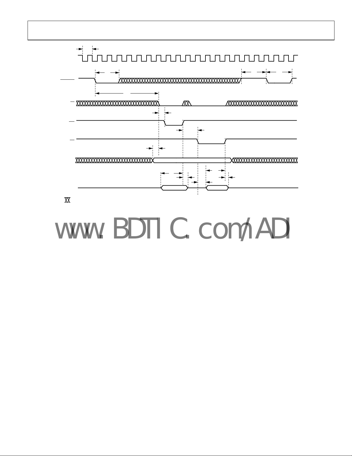
AD2S1210
www.BDTIC.com/ADI
f
CLKIN
CLKIN
t
16
07467-030
SAMPLE
CS
WR
RD
A0, A1
DATA
NOTES
1. DON’T CARE.
t
16
t
17
t
2
t
9
t
1
CONFI GURATION
t
t
19
12
FAULT D ATA
t
3
FAULT ADDRESS
t
4
t
16
t
14A
Figure 31. Parallel Port—Clear Fault Register
Rev. 0 | Page 27 of 36

AD2S1210
www.BDTIC.com/ADI
SERIAL INTERFACE
The serial interface is selected by holding the
AD2S1210 serial interface consists of four signals: SDO, SDI,
WR
FSYNC
/
into the on-chip registers whereas the SDO is used for accessing
data from the on-chip registers, including the position, velocity,
and fault registers. SCLK is the serial clock input for the device,
and all data transfers (either on SDI or SDO) take place with
respect to this SCLK signal.
data. The falling edge of
lines out of a high impedance state. A rising edge on
returns the SDI and SDO to a high impedance state. The
is not required for the serial interface and should be held low.
, and SCLK. The SDI is used for transferring data
WR
FSYNC
/
WR
FSYNC
/
takes the SDI and SDO
SDO Output
In normal mode of operation, data is shifted out of the device as
a 24-bit word under the control of the serial clock input, SCLK.
The data is shifted out on the rising edge of SCLK. The timing
diagram for this operation is shown in Figure 32.
SDI Input
The SDI input is used to address the on-chip registers and as a
daisy-chain input in configuration mode. The data is shifted
into the part on the falling edge of SCLK. The timing diagram
for this operation is shown in Figure 32.
Writing to the AD2S1210
The on-chip registers of the AD2S1210 can be accessed using
the serial interface. To write to one of the registers, the user
must first place the AD2S1210 into configuration mode using
the A0 and A1 inputs. The 8-bit address should be written to
the AD2S1210 using the SDI pin and latched using the rising
WR
edge of the
the SDI pin and again latched into the part using the
input. The MSB of the 8-bit write indicates whether the 8-bit
word is a register address, MSB set high, or the data to be written,
MSB set low. Figure 33 shows the timing specifications to follow
when writing to the configuration registers.
FSYNC
/
input. The data can then be presented on
Reading from the AD2S1210 in Configuration Mode
To read back data stored in one of the on-chip registers, including
the fault register, the user must first place the AD2S1210 into
configuration mode using the A0 and A1 inputs. The 8-bit
address of the register to be read should then be written to the
part, as described in the Writing to the AD2S1210 section.
This transfers the relevant data to the output register.
In configuration mode, the output shift register is eight bits
wide. Data is shifted out of the device as an 8-bit word under
the control of the serial clock input, SCLK. The timing diagram
for this operation is shown in Figure 34. When reading back
data from any of the read/write registers (see Table 10), the 8-bit
word consists of the seven bits of data in the relevant register,
D6 to D0, and an error bit, D7. If the error bit is returned high,
SOE
pin low. The
is used to frame the
WR
FSYNC
/
CS
input
WR
FSYNC
/
this indicates that the data read back from the device does not
match the configuration data written to the device in the previous
write cycle.
To read back the angular position or velocity data while in
configuration mode, a falling edge of the
required to update the information in the position and velocity
registers.
SAMPLE
input is
Reading from the AD2S1210 in Normal Mode
To read back position or velocity data from the AD2S1210, the
information stored in the position and velocity registers should
first be updated using the
transition on the
position and velocity integrators to the position and velocity
registers. The fault register is also updated on the high-to-low
transition of the
inputs determines whether the position or velocity data is
transferred to the output register.
In normal mode, the output shift register is 24 bits wide. The 24-bit
word consists of 16 bits of angular data (position or velocity data)
followed by the 8-bit fault register data. Data is read out MSB
first (Bit 23) on the SDO pin. Bit 23 through Bit 8 correspond to
the angular information. The angular position data format is
unsigned binary, with all 0s corresponding to 0 degrees and all
1s corresponding to 360 degrees − l LSB. The angular velocity data
format is twos complement binary, with the MSB representing the
rotation direction. Bit 7 through Bit 0 correspond to the fault
information. If the user does not require the fault information,
WR
the
FSYNC
/
SAMPLE
SAMPLE
can be pulled high after the16th SCLK rising edge.
SAMPLE
input transfers the data from the
input. The status of the A0 and A1
input. A high-to-low
Clearing the Fault Register
The LOT pin and/or the DOS pin of the AD2S1210 are taken
low to indicate that a fault has been detected. The AD2S1210 is
capable of detecting eight separate fault conditions. To determine
which condition triggered the fault indication, the user is required
to enter configuration mode and read the fault register. To reset
the fault indicators, an additional
This ensures that any faults that may occur between the initial
sampling and subsequent reading of the fault register are captured.
Therefore, to read and clear the fault register, the following
sequence of events is required:
1.
A high-to-low transition of the
2.
Hold the
returned high.
3.
Put the AD2S1210 into configuration mode, that is, A0 and
A1 are both set to logic high.
Read the fault register as described in the Reading from the
4.
AD2S1210 in Configuration Mode section.
5.
A second high-to-low transition of the
clears the fault indications on the DOS and/or LOT pins.
Note that in the event of a persistent fault, the fault indicators
are reasserted within the specified fault time latency.
SAMPLE
input low for t16 ns and then it can be
SAMPLE
SAMPLE
pulse is required.
input.
SAMPLE
input
Rev. 0 | Page 28 of 36
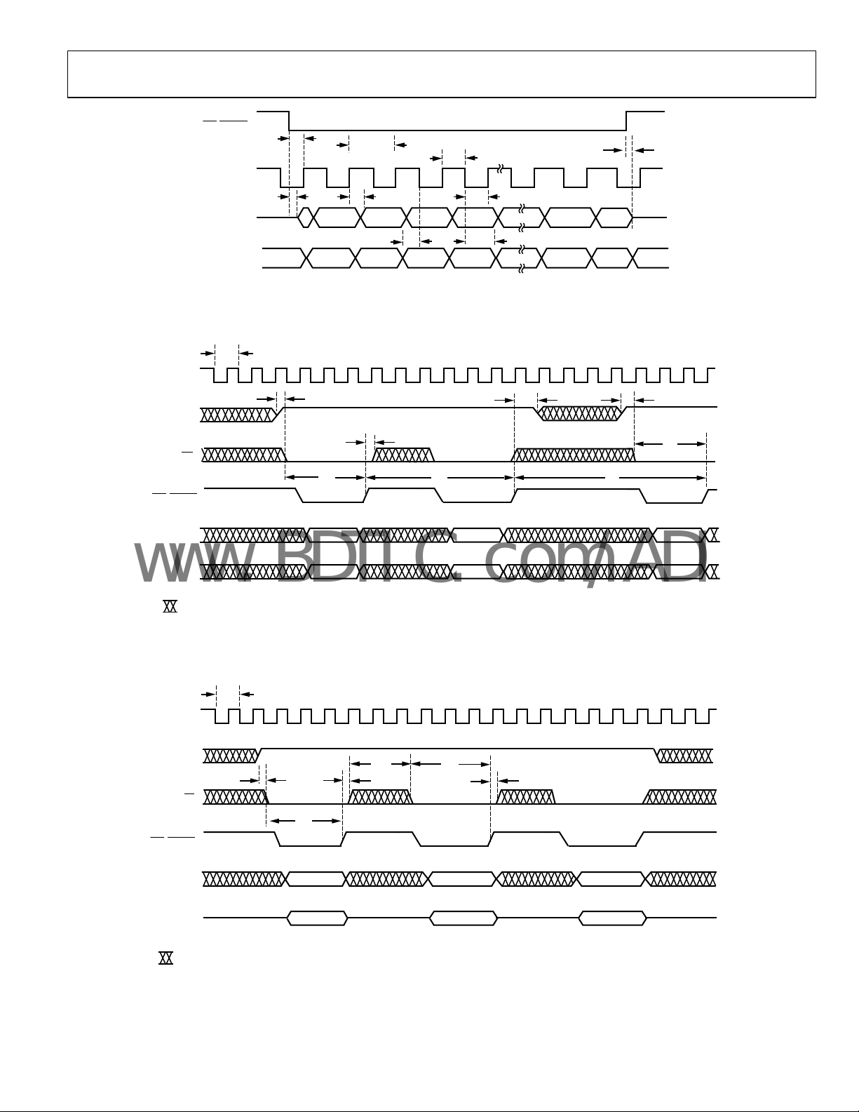
AD2S1210
www.BDTIC.com/ADI
WR/FSYNC
CLKIN
A0, A1
CS
WR/FSYNC
SCLK
SDO
SDI
f
CLKIN
t
22
t
23
f
SCLK
t
24
MSB
t
MSB LSB
t
25
t
26
27
t
28
t
29
LSB
07467-031
Figure 32. Serial Interface Timing Diagram
t
1
t
5
t
2
t
7
t
8
t
1
t
2
t
9
SDI
SDO
NOTES
1. DON’T CARE.
ADDRESS
OLD DATA
DATA
OLD DATA
NEW ADDRESS
COPY OF DATA
07467-032
Figure 33. Serial Interface Write Timing—Configuration Mode
f
CLKIN
CLKIN
A0, A1
CS
WR/FSYNC
SDI
SDO
t
1
ADDRESS 1
OLD DATA
t
2
t
6
t
5
t
2
ADDRESS 2 ADDRESS 3
DATA 1 DATA 2
t
5
NOTES
1.
DON’T CARE.
Figure 34. Serial Interface Read Timing—Configuration Mode
Rev. 0 | Page 29 of 36
07467-033

AD2S1210
*
www.BDTIC.com/ADI
f
CLKIN
CLKIN
t
16
SAMPLE
t
30
CS
t
31
WR/FSYNC
t
32
A0, A1
SDO
ASSUMES FAULT REGISTER ADDRESS WRIT TEN TO PART BEFORE EX ITING CO NFIGURATI ON MODE.
NOTES
1.
DON’T CARE.
t
6
t
34
t
33
VELOCITYPO SITION FAULT*
t
23
VELOCITYPOSITION FAULT*
t
16
t
29
07467-034
Figure 35. Serial Interface Read Timing
Rev. 0 | Page 30 of 36
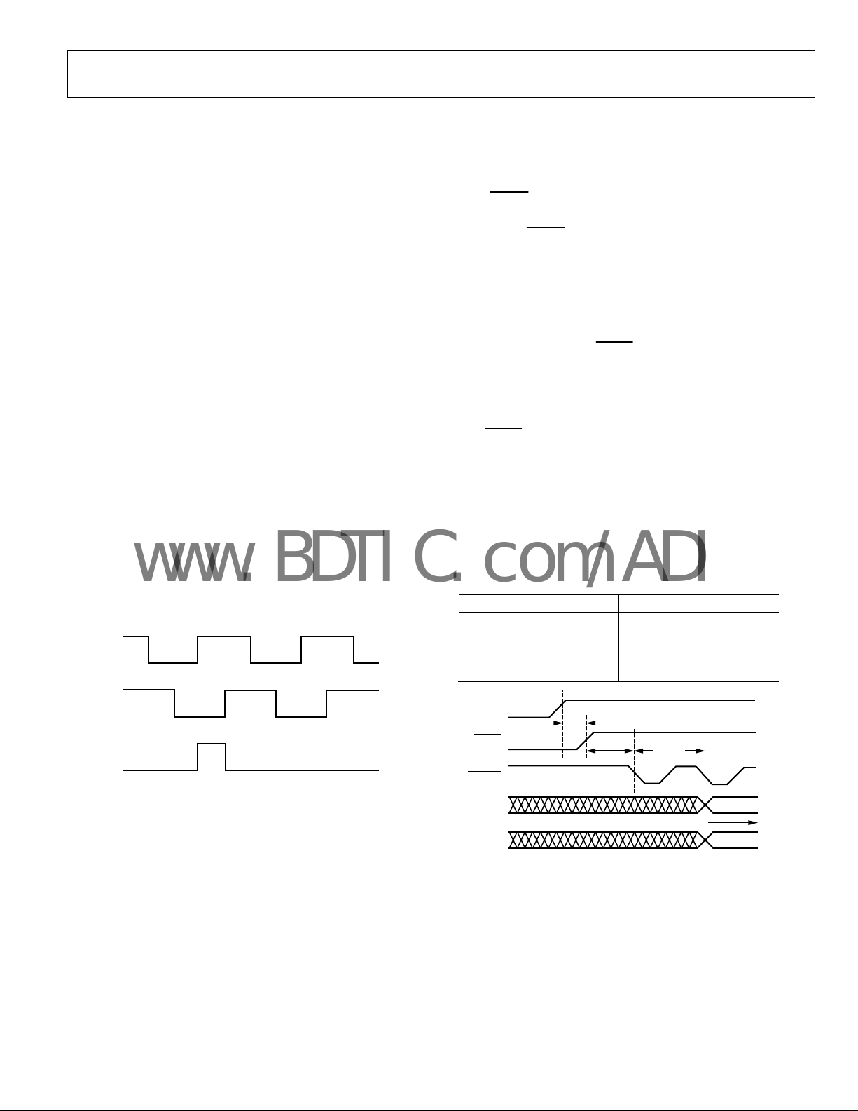
AD2S1210
www.BDTIC.com/ADI
INCREMENTAL ENCODER OUTPUTS
The A, B, and NM incremental encoder emulation outputs are
free running and are valid if the resolver format input signals
applied to the converter are valid.
The AD2S1210 can be configured to emulate a 256-line, a
1024-line, a 4096-line, or a 16,384-line encoder. For example,
if the AD2S1210 is configured for 12-bit resolution, one revolution produces 1024 A and B pulses. Pulse A leads Pulse B for
increasing angular rotation (that is, clockwise direction).
The resolution of the encoder emulation outputs of the AD2S1210
is generally configured to match the resolution of the digital output.
However, the encoder emulation outputs of the AD2S1210 can also
be configured to have a lower resolution than the digital outputs.
For example, if the AD2S1210 is configured for 16-bit resolution, then the encoder emulation outputs can also be configured
for 14-bit, 12-bit, or 10-bit resolution. However, the resolution
of the encoder emulation outputs cannot be higher than the
resolution of the digital output. If the AD2S1210 is configured
such that the resolution of the encoder emulation outputs is
higher than the resolution of the digital outputs, the AD2S1210
internally overrides this configuration. In this event, the resolution of the encoder outputs is set to match the resolution of the
digital outputs. The resolution of the encoder emulation outputs
can be programmed by writing to Bit D3 and Bit D2 of the
control register.
The north marker pulse is generated as the absolute angular
position passes through zero. The north marker pulse width
is set internally for 90° and is defined relative to the A cycle.
Figure 36 details the relationship between A, B, and NM.
A
SUPPLY SEQUENCING AND RESET
The AD2S1210 requires an external reset signal to hold the
RESET
input low until VDD is within the specified operating
range of 4.5 V to 5.5 V.
RESET
The
V
DD
Applying a
position to a value of 0x000 (degrees output through the parallel,
serial, and encoder interfaces) and causes LOS to be indicated
(LOT and DOS pins pulled low), as shown in Figure 37.
Failure to apply the correct power-up/reset sequence may result
in an incorrect position indication.
After a rising edge on the
at least t
ize and the tracking loop to settle to the step change of the input
position. For the duration of t
on the LOT and DOS pins due to the step response caused by
RESET
the
resolution as outlined in Table 27. After t
should be read and cleared as outlined in the Clearing the Fault
Register section. The time required to read and clear the fault
register is indicated as t
speed of the DSP/microprocessor used in the application. (Note
that if position data is acquired via the encoder outputs, these
can be monitored during t
Table 27. t
Resolution (Bits) t
10 10
12 20
14 25
16 60
pin must be held low for a minimum of 10 μs after
is within the specified range (shown as t
RESET
signal to the AD2S1210 initializes the output
RESET
input, the device must be allowed
ms (see Figure 37) for the internal circuitry to stabil-
TRACK
fault indications may occur
TRACK
. The duration of t
FAULT
vs. Resolution (f
TRACK
is dependent on the converter
TRACK
, and is defined by the interface
.)
TRACK
CLKIN
(ms)
TRACK
RST
TRACK
= 8.192 MHz)
in Figure 37).
, the fault register
V
LOT
4.75V
DD
t
RST
B
NM
Figure 36. A, B, and NM Timing for Clockwise Rotation
The inclusion of A and B outputs allows the AD2S1210 with
RESET
07467-035
SAMPLE
resolver solution to replace optical encoders directly without
the need to change or upgrade existing application software.
DOS
Figure 37. Power Supply Sequencing and Reset
Rev. 0 | Page 31 of 36
t
TRACK
t
FAULT
VAL ID
OUTPUT
DATA
07457-036

AD2S1210
c
t
+
+
www.BDTIC.com/ADI
CIRCUIT DYNAMICS
LOOP RESPONSE MODEL
ERROR
(ACCELERATIO N)
θ
IN
k1 × k2
–
Figure 38. RDC System Response Block Diagram
1 – z
Sin/Cos LOOKUP
The RDC is a mixed-signal device that uses two ADCs to digitize
signals from the resolver and a Type II tracking loop to convert
these to digital position and velocity words.
The first gain stage consists of the ADC gain on the sine/cosine
inputs and the gain of the error signal into the first integrator.
The first integrator generates a signal proportional to velocity.
The compensation filter contains a pole and a zero that are used
to provide phase margin and reduce high frequency noise gain.
The second integrator is the same as the first and generates the
position output from the velocity signal. The sin/cos lookup has
unity gain. The values for the k1, k2, a, b, and c parameters are
outlined in Table 28.
The following equations outline the transfer functions of the
individual blocks as shown in Figure 38, which then combine to
form the complete RDC system loop response.
Integrator1 and Integrator2 transfer function
)(
zI (10)
1
−
1
−=z
Compensation filter transfer function
1
−
az
1
−
zC (11)
)(
=
1
−
bz
1
−
RDC open-loop transfer function
2
VELOCITY
1 – bz
–1
–1
1 – z
c
–1
θ
OUT
7467-037
c 1 – az
–1
)()()(
zCzIk2k1zG ×××= (12)
RDC closed-loop transfer function
zG
zH+= (13)
)(
)(
zG
)(1
The closed-loop magnitude and phase responses are that of a
second-order low-pass filter (see Figure 11 and Figure 12).
To convert G(z) into the s-plane, an inverse bilinear transformation is performed by substituting the following equation for z:
2
s
+
t
z
=
(14)
2
−
s
where t is the sampling period (1/4.096 MHz ≈ 244 ns).
Substitution yields the open-loop transfer function, G(s).
22
ts
1
s
st
1
ak2k1
)1(
sG
)(
= (15)
−×
ba
−
++
×
4
2
s
×+
×
×+
1
s
)1(
at
−
)1(2
a
+
)1(
bt
−
)1(2
b
This transformation produces the best matching at low frequencies
(f < f
). At such frequencies (within the closed-loop
SAMPLE
bandwidth of the AD2S1210), the transfer function can be
simplified to
K
sG
)(
s
st
1
a
2
1
×≅ (16)
st
1
+
2
where:
at
+
t
=
1
t
=
2
K
a
)1(
a
−
)1(2
bt
+
)1(
b
−
)1(2
=
−
ak2k1
−×
)1(
ba
Solving for each value gives t
Table 28. RDC System Response Parameters
Parameter Description 10-bit resolution 12-bit resolution 14-bit resolution 16-bit resolution
k1 (nominal) ADC gain 1.8/2.5 1.8/2.5 1.8/2.5 1.8/2.5
k2 Error gain
6
× 2π 18 × 106 × 2π 82 x 106 × 2π 66 × 106 × 2π
6 × 10
a Compensator zero coefficient 8187/8192 4095/4096 8191/8192 32,767/32,768
b Compensator pole coefficient 509/512 4085/4096 16,359/16,384 32,757/32,768
c Integrator gain 1/1,024,000 1/4,096,000 1/16,384,000 1/65,536,000
Rev. 0 | Page 32 of 36
, t2, and Ka as outlined in Table 29.
1

AD2S1210
www.BDTIC.com/ADI
Table 29. Loop Transfer Function Parameters vs. Resolution
= 8.192 MHz)
(f
CLKIN
Resolution (Bits) t1 (ms) t2 (ms) Ka (sec−2)
10 0.4 42 39.6 × 10⁶
12 1 91 6.5 × 10⁶
14 2 160 1.6 × 10⁶
16 8 728 92.7 × 10³
Note that the closed-loop response is described as
)(
sG
)(
sH+=
By converting the calculation to the s-domain, it is possible to
quantify the open-loop dc gain (K
calculate the acceleration error of the loop (see the Sources of
Error section).
The step response to a 10° input step is shown in Figure 10,
Figure 11, Figure 12, and Figure 13. The step response to a 179°
input step is shown in Figure 14, Figure 15, Figure 16, and
Figure 17. In response to a step change in velocity, the
AD2S1210 exhibits the same response characteristics as it does
for a step change in position.
Figure 18 and Figure 19 in the Typical Performance
Characteristics section show the magnitude and phase responses
of the AD2S1210 for each resolution setting.
)(1
sG
). This value is useful to
a
(17)
SOURCES OF ERROR
Acceleration
A tracking converter employing a Type II servo loop does not
have a lag in velocity. There is, however, an error associated
with acceleration. This error can be quantified using the
acceleration constant (K
K
=
a
Conversely,
ErrorTracking =
The units of the numerator and denominator must be consistent.
The maximum acceleration of the AD2S1210 is defined by the
maximum acceptable tracking error in the users application.
For example, if the maximum acceptable tracking error is 5°,
then the maximum acceleration is defined as the acceleration that
creates an output position error of 5° (that is, when LOT is
indicated).
An example of how to calculate the maximum acceleration in a
12-bit application with a maximum tracking error of 5° is
Figure 20 to Figure 23 in the Typical Performance
Characteristics section show the tracking error vs. acceleration
response of the AD2S1210 for each resolution setting.
) of the converter.
a
onAcceleratiInput
ErrorTracking
(18)
K
a
K
a
=
onAcceleratiMaximum
(20)
onAcceleratiInput
(19)
−
2
°×
5)(sec
≅
)/rev(360
90,300 rps
°
2
Rev. 0 | Page 33 of 36

AD2S1210
www.BDTIC.com/ADI
OUTLINE DIMENSIONS
9.20
1
12
0.50
BSC
48
13
9.00 SQ
8.80
PIN 1
TOP VIEW
(PINS DO WN)
37
24
0.27
0.22
0.17
36
7.20
7.00 SQ
6.80
25
051706-A
1.45
1.40
1.35
0.15
SEATING
0.05
PLANE
VIEW A
ROTATED 90° CCW
0.75
0.60
0.45
0.20
0.09
7°
3.5°
0°
0.08
COPLANARIT Y
COMPLIANT TO JEDEC STANDARDS MS-026-BBC
1.60
MAX
VIEW A
LEAD PITCH
Figure 39. 48-Lead Low Profile Quad Flat Package [LQFP]
(ST-48)
Dimensions shown in millimeters
ORDERING GUIDE
Model Temperature Range Package Description Package Option
AD2S1210ASTZ1 −40°C to +85°C 48-Lead LQFP ST-48
AD2S1210BSTZ1 −40°C to +85°C 48-Lead LQFP ST-48
AD2S1210CSTZ1 −40°C to +125°C 48-Lead LQFP ST-48
AD2S1210DSTZ1 −40°C to +125°C 48-Lead LQFP ST-48
1
Z = RoHS Compliant Part.
Rev. 0 | Page 34 of 36

AD2S1210
www.BDTIC.com/ADI
NOTES
Rev. 0 | Page 35 of 36

AD2S1210
www.BDTIC.com/ADI
NOTES
©2008 Analog Devices, Inc. All rights reserved. Trademarks and
registered trademarks are the property of their respective owners.
D07467-0-8/08(0)
Rev. 0 | Page 36 of 36
 Loading...