Integrated Digital
a
FEATURES
Complete EIAJ CP-340 (CP-1201), IEC-958, AES/EBU,
S/PDIF Compatible Digital Audio Receiver and
Asynchronous Sample Rate Converter
Status Pins and Microprocessor Interfaces for
Stand-Alone and Microcontroller-Oriented Operation
Integrated Channel Status Buffer and Q-Channel
Subcode Buffer (Supports EIAJ CP-2401)
20-Bit SamplePort
Rejection on Input Port
Sample Rate Conversion from 8 kHz to 48 kHz with
1:5 Upsampling Range
1:0.85 Downsampling Range
120 dB Dynamic Range
–113 dB THD+N @ 1 kHz
CRC Calculation on Q-Channel Subcode (Consumer
Mode Only) and on Channel Status (Pro Mode Only)
Four-Wire SPI™ Compatible Serial Control Port
Mute Input Pin
Power-Down Mode
Single +5 V Supply
Flexible Three-Wire Serial Data Port with Left-Justified,
Right-Justified and I
28-Lead SOIC Package
APPLICATIONS
DVD, DAT, MD, DCC and CD-R Recorders and Players
Computer Multimedia Products
DAB Receivers, Automotive Digital Audio Networks
®
Architecture Provides Superb Jitter
2
S-Compatible Modes
Receiver/Rate Converter
AD1892
PRODUCT OVERVIEW
The AD1892 combines a CP-1201, CP-340, IEC-958, AES/
EBU, S/PDIF compatible Digital Audio Receiver (DAR) with
an asynchronous sample rate converter, allowing the user to
specify the output sample rate of the received digital audio information. The DAR block features support for both Q-channel
subcode information (to support CD, CD-R, MD and DAT
digital audio formats) as well as Channel Status information. A
microcontroller interface, with an SPI compatible serial port,
allows full access to the 80-bit Q-Channel subcode buffer and to
the 32-bit Channel Status buffer, as well as to the control and
status registers. Additionally, key status information from the
incoming subframes and the Channel Status buffer is reported
on status output pins on the AD1892, so the AD1892 may be
used in systems that do not include a microcontroller or
microprocessor.
The asynchronous sample rate converter block is based on
market leading AD1890 family SamplePort
nology. The AD1892 offers a 1:5 upsampling range, and will
downsample from 48 kHz to 44.1 kHz. Input audio word widths
up to 20 bits are supported, and output audio word widths of 16
or 20 are supported, with 120 dB of dynamic range and –113 dB
THD+N. The rate converter inherently rejects jitter on the
recovered clocks from the incoming biphase-mark encoded
stream. Indeed, sample rate conversion is highly synergistic
with digital audio reception, allowing the use of a fully digital
phase locked loop clock recovery scheme with highly robust
clock recovery and jitter rejection.
rate conversion tech-
(continued on Page 4)
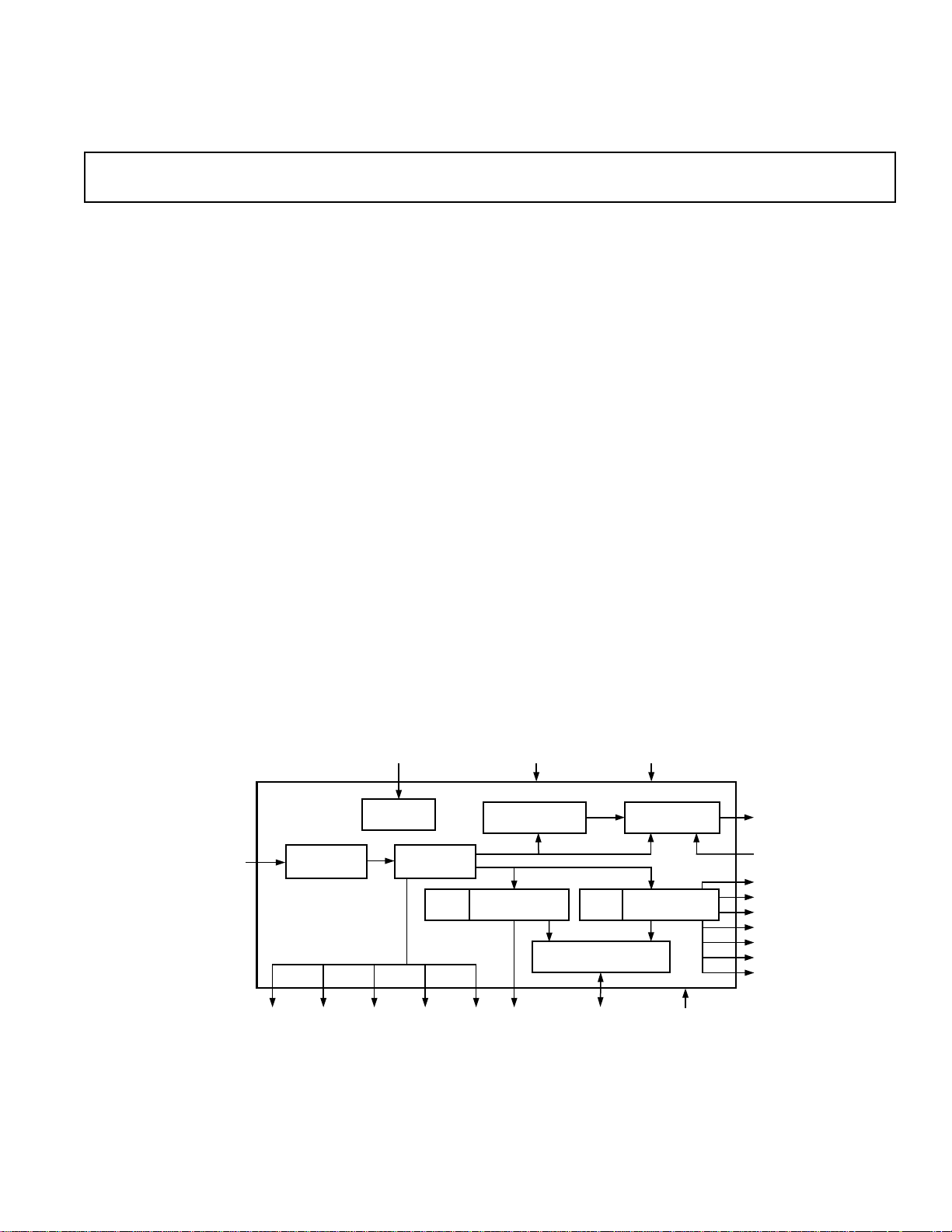
FUNCTIONAL BLOCK DIAGRAM
512 x F
SOUT
CLOCK
GENERATOR
INPUT
2
SIGNAL
BIPHASE-MARK
NO
RECEIVER
AD1892
ERROR
INTERRUPT
COMPARATOR
CRC
CHECK
U/C BIT SFCLK
BIPHASE-MARK
SamplePort is a registered trademark of Analog Devices, Inc.
SPI is a trademark of Motorola, Inc.
REV. 0
Information furnished by Analog Devices is believed to be accurate and
reliable. However, no responsibility is assumed by Analog Devices for its
use, nor for any infringements of patents or other rights of third parties
which may result from its use. No license is granted by implication or
otherwise under any patent or patent rights of Analog Devices.
POWER-DOWN/RESET
ASYNCH SAMPLE
RATE CONVERTER
DATA
CONTROL
Q-CHANNEL
SUBCODE BUFFER
QDFS
One Technology Way, P.O. Box 9106, Norwood, MA 02062-9106, U.S.A.
Tel: 781/329-4700 World Wide Web Site: http://www.analog.com
Fax: 781/326-8703 © Analog Devices, Inc., 1998
CRC
CHECK
MICROCONTROLLER
INTERFACE
CLOCK, LATCH,
DATA IN,
DATA OUT
MUTE
BCLK
OUTPUT SERIAL
INTERFACE
BYPASS
CHANNEL STATUS
BUFFER
42
DIGITAL
SUPPLY
3
LRCLK
SDATA
SYNC
CA
CB
CC
CD
CE
CON/PRO
CSCLK

AD1892–SPECIFICATIONS
TEST CONDITIONS UNLESS OTHERWISE NOTED
Supply Voltage +5.0 V
Ambient Temperature 25 °C
Output Sample Frequency (F
MCLK 25 MHz (512 × F
Input Word Width 20 Bits
Load Capacitance 100 pF
All minimums and maximums tested except as noted.
) 48.8 kHz
SOUT
SOUT
)
PERFORMANCE
1
Min Typ Max Units
Dynamic Range (20 Hz to 20 kHz, –60 dB Input) 120 dB
Total Harmonic Distortion + Noise
(20 Hz to 20 kHz, Full-Scale Input) –103 dB
(1 kHz Full-Scale Input) –113 dB
(10 kHz Full-Scale Input) –107 dB
Interchannel Phase Deviation 0 Degrees
DIGITAL I/O
1
Min Typ Max Units
V
IH
V
IL
@ V
I
IH
I
IL
V
OH
V
OL
Input Capacitance
DIGITAL TIMING
= +5.0 V 10 µA
IH
@ V
= 0 V 10 µA
IL
@ IOH = –0.5 mA DVDD – (0.5) V
@ IOL = 0.5 mA 0.5 V
1
1
2.4 V
0.8 V
15 pF
Min Typ Max Units
t
MCP
F
MCLK
t
PDRP
t
BDM
t
LDM
t
DDP
t
DDS
t
DDH
t
SSU
t
CCH
t
CCL
t
CCP
t
CSU
t
CHD
t
COH
t
SFPW
t
SFSU
t
CSPW
t
QDH
t
CLH
t
CLK
t
RS
MCLK Duty Cycle
MCLK Frequency (1/t
PD/RST LO Pulsewidth 10 × MCLK Period ns
BCLK Propagation Delay from MCLK (to Falling Edge) 30 ns
LRCLK Propagation Delay from MCLK 30 ns
Data Propagation Delay from MCLK 30 ns
Data Output Setup to BCLK 1/2 BCLK Period ns
Data Output Hold from BCLK 1/2 BCLK Period ns
SYNC Falling Setup to MCLK Rising 5 ns
CCLK HI Pulsewidth 20 ns
CCLK LO Pulsewidth 20 ns
CCLK Period 8 × MCLK Period ns
SDI Setup 15 ns
SDI Hold 10 ns
SDO Propagation Delay from CCLK 30 ns
SFCLK HI Pulsewidth
U/CBIT, INT, ERROR Setup to SFCLK 100 ns
CSCLK HI Pulsewidth
QDFS HI Pulsewidth
CS HI Pulsewidth 10 × MCLK Period ns
CS Falling Edge to CCLK Rising 3 × MCLK Period ns
PD/RST Rising to MCLK Rising Edge (Only Required
1
1
)
MCP
1
1
1
40 60 %
25 MHz
100 ns
100 ns
1000 ns
for Synchronizing Multiple Parts) 5 ns
DIGITAL RS-422 RECEIVERS (RXP, RXN Pins Only)
Min Typ Max Units
Input Resistance 20 kΩ
Min Differential AES/EBU or S/PDIF Input 200 mV p-p
Input Hysteresis 20 mV
REV. 0–2–
POWER
WARNING!
ESD SENSITIVE DEVICE
Min Typ Max Units
Supplies
Voltage, DV
DD
Operational Current, I
Power-Down Current, I
Dissipation
1
(DVDD = +5.0 V) 50 60 mA
DD
(DVDD = +5.0 V) (PD/RST LO) 3 6 mA
DD
4.5 5.5 V
Operational (DVDD = +5.0 V) 250 300 mW
Power-Down (DVDD = +5.0 V) (PD/RST LO) 15 30 mW
TEMPERATURE RANGE
Min Max Units
Specifications Guaranteed –40 +85 °C
Storage –55 +125 °C
AD1892
ABSOLUTE MAXIMUM RATINGS
2
Min Max Units
DV
to DGND –0.3 7.0 V
DD
DC Input Voltage –0.3 DV
+ 0.3 V
DD
Soldering +300 °C
10 sec
DIGITAL FILTER CHARACTERISTICS
1
Min Max Units
Passband Ripple (0 kHz to 20 kHz) (F
= 44.1 kHz) ±0.015 dB
S
Group Delay (LRCLK = 50 kHz) 700 3000 µs
NOTES
1
Guaranteed, not tested.
2
Stresses greater than those listed under Absolute Maximum Ratings may cause permanent damage to the device. This is a stress rating only; functional operation of
the device at these or any other conditions above those indicated in the operational section of this specification is not implied. Exposure to absolute maximum rating
conditions for extended periods may affect device reliability.
Specifications subject to change without notice.
ORDERING GUIDE
Model Temperature Range Package Description Package Options
AD1892JR –40°C to +85°C 28-Lead SOIC R-28
AD1892JRRL –40°C to +85°C 28-Lead SOIC R-28 on 13" Reels
CAUTION
ESD (electrostatic discharge) sensitive device. Electrostatic charges as high as 4000 V readily
accumulate on the human body and test equipment and can discharge without detection.
Although the AD1892 features proprietary ESD protection circuitry, permanent damage may
occur on devices subjected to high energy electrostatic discharges. Therefore, proper ESD
precautions are recommended to avoid performance degradation or loss of functionality.
REV. 0
–3–
AD1892
(continued from Page 1)
PRODUCT OVERVIEW (Continued)
In addition to the Q-channel subcode and Channel Status buffers, the AD1892 includes two 8-bit control registers and two 8bit status registers. The output data interface may be configured
in left-justified, I
2
S-justified and right-justified modes. The
AD1892 includes hardware power-down/reset and mute control
inputs, and power-down/reset and mute may also be invoked
through write to bits in the control registers. The AD1892
operates from a master clock that must be synchronous with the
output sample rate at 512 × F
. Cyclic Redundancy Coding
S
(CRC) error detection is performed over the full 80 bits of the
received Q-channel subcode information in consumer mode, as
well as the full 192 bits of the received Channel Status information in professional mode.
The AD1892 includes a SYNC input (Pin 23) that allows
multiple AD1892s in a system to be synchronized to a common
LEFT/RIGHT clock.
The AD1892 is offered in a 28-lead SOIC package. It operates
over the industrial temperature range from –40°C to +85°C
at a supply voltage from 4.5 V to 5.5 V. The only external
components required to support the AD1892 are power supply
decoupling capacitors.
DEFINITIONS
Dynamic Range
The ratio of a full-scale input signal to the integrated noise in the
passband (0 kHz to ≈20 kHz), expressed in decibels (dB).
Dynamic range is measured with a –60 dB input signal and
“60 dB” arithmetically added to the result. This measurement
technique is consistent with the recommendations of the Audio
Engineering Society (AES17-1991) and the Electronic Industries
Association of Japan (EIAJ CP-307).
Total Harmonic Distortion + Noise
Total Harmonic Distortion plus Noise (THD+N) is defined as
the ratio of the square root of the sum of the squares of the
values of the harmonics and noise to the value of the fundamental input frequency. It is usually expressed in percent (%) or
decibels.
Interchannel Phase Deviation
Difference in input sampling times between stereo channels,
expressed as a phase difference in degrees between 1 kHz inputs.
Group Delay
The time interval required for the frequency components of an
input pulse to appear at the converter’s output, expressed in
milliseconds (ms). More precisely, the derivative of radian phase
with respect to radian frequency at a given frequency.
AD1892 PIN LIST
Biphase-Mark Serial Input
Pin Name SOIC I/O Description
RXP 13 I Positive differential biphase-mark serial digital audio receiver input. 20 mV hysteresis.
RXN 14 I Negative differential biphase-mark serial digital audio receiver input. 20 mV hysteresis.
Serial Output Interface
Pin Name SOIC I/O Description
SDATA 24 O Serial output, MSB first, containing two channels of 16 to 20 bits (default) of twos-complement
data per channel, depending on control register settings. The data can be configured in I
2
S-justified
(default), left-justified, and right-justified orientations, depending on control register settings. See
Figure 36 for timing.
BCLK 26 O Bit clock output for output data. Frequency is either 32 × F
(packed mode) or 64 × F
S
(default),
S
depending on control register settings. See Figure 36 for timing.
LRCLK 25 O LEFT/RIGHT clock output for output data. Runs continuously and is a synchronous divide-down
from MCLK (MCLK/512). See Figure 36 for timing.
SYNC 23 I The SYNC input allows multiple AD1892s in a system to be phase and group delay synchronized to
the same LEFT/RIGHT clock. The SYNC signal resets internal AD1892 counters such that 512 MCLK
cycles after the falling edge of SYNC, the AD1892 data will be valid, and the AD1892 LRCLK signal
will change state. It is recommended that the SYNC input be used only when the AD1892 is in the
64 × F
Decoded Channel Status Outputs
BCLK mode (default configuration). GND when not in use.
SOUT
Pin Name SOIC I/O Description
CA 21 O In consumer or professional mode, CA is the inverse of Channel Status Bit 1, Byte 0 (C1, audio/
nonaudio). CA = 0 indicates nonaudio, CA = 1 indicates audio. CA = 0 can be used to indicate
Dolby AC-3 encoded data.
CB 20 O In consumer mode, CB is the inverse of Channel Status Bit 2, Byte 0 (C2, copy/copyright). CB = 0
indicates copy permitted/copyright not asserted; CB = 1 indicates copy inhibited/copyright asserted.
In professional mode, CB is defined as EM0, the least significant bit of the two bits that encodes the
emphasis status of the audio material.
–4–
REV. 0
AD1892
Decoded Channel Status Outputs (Continued)
Pin Name SOIC I/O Description
CC 19 O In consumer mode, CC is the inverse Channel Status Bit 3, Byte 0 (C3, pre-emphasis). CC = 0
indicates that the audio material has been pre-emphasized; CC = 1 indicates that the audio material
has not been pre-emphasized.
In professional mode, CC is the most significant bit of the two bits that encodes the emphasis status
of the audio material.
Table I illustrates the professional mode emphasis encoding.
Table I. Professional Mode Emphasis Encoding
AD1892 BYTE 0
Output Channel Status Bit
CC CB C2 C3 C4 Status
1 1 0 0 0 Emphasis not indicated. Receiver defaults to
no emphasis with manual override enabled.
1 0 1 0 0 None. Receiver manual override disabled.
0 1 1 1 0 50/15 µs. Receiver manual override disabled.
0 0 1 1 1 CCITT J. 17. Receiver manual override disabled.
CD 18 O In consumer mode, CD indicates that the audio material is original over all category codes. The
state of this bit is affected by both the generation status “L” bit (Channel Status Bit 15, Byte 1) and
the category code (Channel Status Bits 8 through 14, Byte 1) since the definition of the L bit is reversed for three of the category codes (001XXXX, 0111XXX, and 100XXXX). CD = 0 indicates
that the audio material is original. CD = 1 indicates that the audio material is a copy (first generation or higher).
In professional mode, CD is the inverse of Channel Status Bit 9, Byte 1. CD provides some information about channel mode. See below for additional details.
CE 17 O In consumer mode, CE indicates the so-called “ignorant” category codes of “general” (0000 000)
and “A/D converter without copyright information” (0110 000). CE = 1 indicates that the audio
material is not encoded using an ignorant category code. CE = 0 indicates that the audio material is
encoded using an ignorant category code. This status output can be used in conjunction with the
CD output (Pin 18) to implement SCMS copy protection. See below for additional details.
In professional mode, CE indicates a Cyclic Redundancy Code (CRC) check error. CE = 0 indicates that the calculated CRC value does not match the received CRC value. CE = 1 indicates that
the calculated CRC value does match the received CRC value. CE may be used to enable the display of the CA through CD states. If CE = 0, then CA through CD may be considered to be in
error, and their display should not be updated.
The Table II summarizes the function of the CA through CE pins, depending on the operating mode
(professional or consumer).
Table II. Decoded Channel Status Output Functions
Pin Consumer Professional
CA 0 = Audio, 1 = Nonaudio 0 = Audio, 1 = Nonaudio
CB 0 = Copy Permitted, 1 = Copy Inhibited Pre-emphasis Encoding
CC 0 = Pre-emphasis, 1 = No Pre-emphasis Pre-emphasis Encoding
CD 0 = Original, 1 = Copy Inverse of Channel Status Bit 9
CE 0 = Ignorant Category, 1 = Not Ignorant 0 = C.S. CRC Error, 1 = No C.S. CRC Error
PRO 15 O CON/PRO is defined as the inverse Channel Status bit 0, byte 0 (C0, pro/consumer). CON/PRO =
CON/
0 indicates professional mode. CON/PRO = 1 indicates consumer mode. The state of this pin internally determines the consumer/pro mode of the CA, CB, CC, CD and CE pins.
CSCLK 16 O Channel Status Clock. Active HI (rising edge active). Outputs a pulse every 192 frames at the
start of the Channel Status block. Use the falling edge of this clock to latch the CA through CE
and CON/PRO output Channel Status signals. See Figure 38 for timing.
REV. 0 –5–
AD1892
Subframe Status Outputs
Pin Name SOIC I/O Description
NOSIG 12 O NOSIG (No Signal) is asserted HI when no biphase-mark input is applied to the AD1892 when
either the input sample rate is too high for the applied master clock (MCLK) frequency or, equivalently, the master clock frequency is too low for the applied input sample rate. NOSIG is deasserted
LO during normal operation. This signal is asynchronous and has no particular timing relationship
with any of the clock signals associated with the AD1892.
ERROR 11 O The ERROR pin is asserted HI when either a subframe parity error or a subframe validity error
occurs. Logically, ERROR = PARITY ERROR or VALIDITY ERROR. The ERROR pin is deasserted LO when neither parity nor validity errors are detected. The state of this output pin is not
directly reflected in the AD1892 status registers; rather, Status Register 0 has separate bits that
indicate parity and validity errors. The ERROR output should be clocked using the SFCLK signal
(Pin 8). The ERROR output signal is NOT sticky, so it can be used in applications that do not include a supporting microcontroller.
INT 10 O INT (Interrupt) is asserted HI when any of the first 32 bits of Channel Status information changes
from block to block or when the Q-Channel subcode track number (Q10 through Q17) changes
from block to block (valid in consumer mode only). The Channel Status block spans 192 frames (or
subframes, since either the left or right channel C bit is stored), and the Q-Channel subcode block
spans 1176 subframes. INT is deasserted LO when neither the first 32 bits of Channel Status
changes from block to block when the Q-Channel subcode track number changes from block to
block. This output is mirrored in a status bit (Status Register 0, Bit 5). The INT output can be
clocked using the SFCLK signal (Pin 8). The INT output signal is sticky and can only be cleared by
reading Status Register 0.
U/CBIT 9 O U/CBIT is either the subframe user bit or the Channel Status bit from the biphase-mark stream, fed
out serially, valid on the rising edge of the SFCLK signal (Pin 8). The choice between user bit and
Channel Status bit is determined by Bit 1 in Control Register 0 (0 user bit [default], 1 = Channel
Status bit). Changes at the subframe rate (two times the incoming sample rate.) See Figure 39 for
timing.
SFCLK 8 O This SFCLK signal is used to clock the ERROR, INT and U/CBIT output status signals. Active
LO (rising edge active); see Figure 39 for timing. It is a LO pulse at the subframe rate (two times
the sample rate). The pulsewidth is approximately 1/64th of the incoming sample (frame) period.
Q-Channel Subcode Clock Output Signal
Pin Name SOIC I/O Description
QDFS 6 O QDFS (Q-Channel Data Frame Sync) is a framing pulse indicating if the AD1892 has finished col-
lecting a full Q-Channel subcode block of user bits, which has a period of 1176 subframes. Can be
used as an interrupt signal to a microcontroller. The QDFS output is HI for one subframe period.
The QDFS frequency is 75 Hz when the incoming input sample rate is 44.1 kHz. See Figure 40 for
timing information.
Serial Control Port Signals
Pin Name SOIC I/O Description
CS 3 I Chip Select/Latch signal for the serial control port. This input must be LO for any write or read
operation using the serial control port to be valid. This input should be tied HI when using the
AD1892 in a stand-alone (no external microcontroller) application. See the Serial Control Port
Timing in Figure 37 and the text below for more information.
CCLK 2 I Serial Control Port Clock. This rising edge active input samples the address and data associated
with the serial control port. The frequency of CCLK signal must not exceed 1/8 the frequency of
the MCLK (Pin 28) signal. See the Serial Control Port Timing in Figure 37 and the text below for
more information.
SDI 4 I Serial Data Input. This input signal is used to convey the serial 6-bit address, the read/write indication
and the 8-bit write data for the AD1892 serial control port. See the Serial Control Port Timing in
Figure 37 and the text below for more information.
SDO 5 O Serial Data Output. This three-state output is used to convey the serial 8-bit read data for the
AD1892 serial control port. It is a three-state output to allow multiple AD1892s to coexist on the same
SPI serial bus. See the Serial Control Port Timing in Figure 37 and the text below for more information.
–6–
REV. 0
AD1892
Power Supply Connections
Pin Name SOIC I/O Description
DV
DD
DGND 7 Digital Ground. +0 V nominal supply connection.
Miscellaneous
Pin Name SOIC I/O Description
MCLK 28 I Master clock. Must be 512 × F
PD/RST 1 I Active LO power-down/reset, which clears all on-chip registers on the AD1892 to their default state
MUTE 27 I Mute input. HI hardware mutes the serial digital audio output to zeros (midscale). All control
22 Digital Supply. +5 V nominal supply voltage.
, where F
SOUT
SOUT
and stops the on-chip clocks. Bring HI for normal chip operation.
functions on the AD1892 (Channel Status, Q-Channel subcode, etc.) continue to function while the
AD1892 is muted. Should be LO for normal operation.
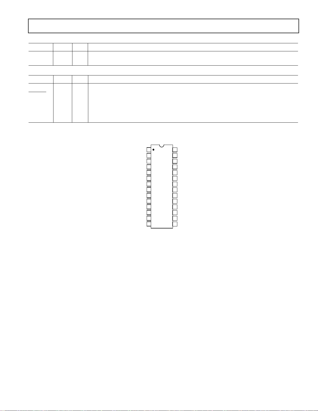
PIN CONFIGURATION
is the desired output sample rate.
PD/RST
CCLK
CS
SDI
SDO
QDFS
DGND
SFCLK
U/CBIT
INT
ERROR
NOSIG
RXP
RXN
1
2
3
4
5
6
TOP VIEW
(Not to Scale)
7
8
9
10
11
12
13
14
AD1892
MCLK
28
MUTE
27
26
BCLK
25
LRCLK
24
SDATA
23
SYNC
22
DV
21
CA
20
CB
19
CC
18
CD
17
CE
16
CSCLK
15
CON/PRO
DD
REV. 0 –7–
AD1892
PREAMBLES
X LEFT CH Y RIGHT CH Z LEFT CH Y RIGHT CH X LEFT CH Y RIGHT CH X
FRAME 191
FRAME 0
FRAME 1
START OF CHANNEL STATUS BLOCK
SUB-
FRAME
SUB-
FRAME
PREAMBLE X
PREAMBLE Y
PREAMBLE Z
11011000
11001010
11101000
SERIAL DIGITAL AUDIO TRANSMISSION STANDARDS
The AD1892 can receive S/PDIF (Sony/Philips Digital Interface
Format), AES/EBU (Audio Engineering Society/European
Broadcasting Union, also known as AES3-1992), IEC-958
(International Electrotechnical Commission) and CP-340 (EIAJ
[Electronic Industry Association of Japan] CP-1201) serial
streams. S/PDIF is a consumer audio standard, and AES/EBU
is a professional audio standard; IEC-958 and CP-340 have
both consumer and professional definitions. This data sheet is
not intended to fully define or to provide a tutorial for these
standards; please contact these international standards setting
bodies for the full specifications.
All of these digital audio serial communication schemes encode
audio data and audio control information using the biphasemark method. This encoding method minimizes the dc content
of the transmitted signal and allows the receiver to decode clock
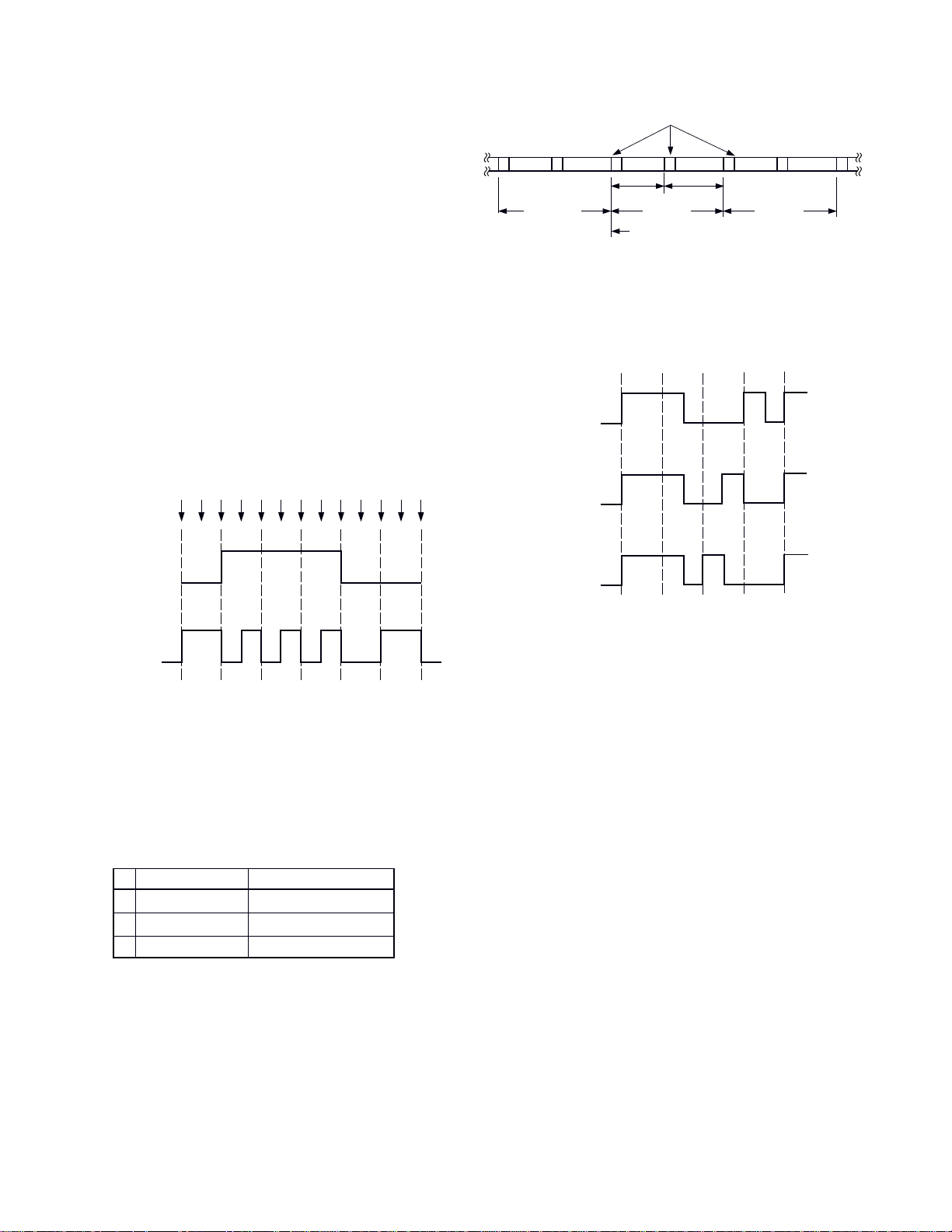
information from the transmitted signal. As can be seen from
Figure 1, ones in the original data end up with midcell transitions in the biphase-mark encoded data, while zeros in the original data do not. Note that the biphase-mark encoded data
always has a transition between bit boundaries.
Figure 3. Preambles, Frames and Subframes
The biphase-mark encoding violations are shown in Figure 4.
Note that all three preambles include encoding violations. Ordinarily, the biphase-mark encoding method results in a polarity
transition between bit boundaries.
(2 TIMES BIT RATE)
CLOCK
DATA
BIPHASE-MARK
DATA
011100
1
01001010111
Figure 1. Biphase-Mark Encoding
Digital audio communication schemes use “preambles” to distinguish between channels (called “subframes”) and between
longer term control information blocks (called “frames”). Preambles are particular biphase-mark patterns, which contain
encoding violations that allow the receiver to uniquely recognize
them. These patterns, and their relationship to frames and
subframes, are shown in Figures 2 and 3.
BIPHASE PATTERNS
11100010 OR 00011101
X
11100100 OR 00011011
Y
11101000 OR 00010111
Z
CHANNEL
LEFT
RIGHT
LEFT AND C.S. BLOCK START
Figure 4. Preambles
As noted above, these serial digital audio communication
schemes are organized using a frame and subframe construction.
There are two subframes per frame (ordinarily the left and right
channel). Each subframe includes the appropriate four bit
preamble, four bits of “auxiliary” (aux) data, 20 bits of audio
data (LSB first), a “validity” (V) bit, a “user” (U) data bit, a
Channel Status (C) bit and an even parity (P) bit. The Channel
Status bits and the user bits accumulate over many frames to
convey control information. The Channel Status bits accumulate over a 192 frame period (called a Channel Status block).
The user bits accumulate over 1176 frames when the interconnect is implementing the so-called “subcode” scheme
(EIAJ CP-2401). The organization of the Channel Status
block, frames and subframes is shown in Figure 5.
Figure 2. Biphase-Mark Encoded Preambles
–8–
REV. 0
 Loading...