Analog Devices AD1886AJST Datasheet

a
AC’97 SoundMAX® Codec
AD1886A
AC’97 2.1 FEATURES
Variable Sample Rate Audio
Multiple Codec Configuration Options
External Audio Power-Down Control
AC’97 FEATURES
AC’97 2.2 Compliant
Greater than 90 dB Dynamic Range
Stereo Headphone Amplifier
Multibit ⌺-⌬ Converter Architecture for Improved S/N
Ratio Greater than 90 dB
16-Bit Stereo Full-Duplex Codec
Four Analog Line-Level Stereo Inputs for:
LINE-IN, CD, VIDEO, and AUX
Two Analog Line-Level Mono Inputs for Speakerphone
and PC BEEP
Mono MIC Input w/Built-In 20 dB Preamp, Switchable
from Two External Sources
High-Quality CD Input with Ground Sense
FUNCTIONAL BLOCK DIAGRAM
ID1
ID0
0dB/
20dB
VREF
CHIP SELECT
⌺
⌺
PHAT
STEREO
G
A
M
⌺
PHONE_IN
MONO_OUT
HP_OUT_L
LINE_OUT_L
V
REFOUT
VIDEO
MIC1
MIC2
LINE
AUX
CD
MV
MV
MV
JS
JACK SENSE
⌺
Stereo Line Level Outputs
Mono Output for Speakerphone or Internal Speaker
Power Management Support
48-Terminal LQFP Package
ENHANCED FEATURES
20-Bit SPDIF Output w/32 kHz, 44.1 kHz, and 48 kHz
Symbol Rates
Full Duplex Variable Sample Rates from 7040 Hz to
48 kHz with 1 Hz Resolution
Jack Sense Pins Provide Automatic Output Switching
Software-Enabled V
Output for Microphones and
REFOUT
External Power Amp
Split Power Supplies (3.3 V Digital/5 V Analog)
Mobile Low-Power Mixer Mode
Extended 6-Bit Master Volume Control
Extended 6-Bit Headphone Volume Control
Digital Audio Mixer Mode
Phat™ Stereo 3D Stereo Enhancement
SPDIF
G
G
A
A
M
M
⌺⌺⌺⌺
AD1886A
16-BIT
PGA
SELECTOR
PGA
G
G
G
A
A
A
M
M
M
G
⌺
⌺
A
M
⌺-⌬ A/D
CONVERTER
16-BIT
⌺-⌬ A/D
CONVERTER
SAMPLE
RATE
GENERATORS
16-BIT
⌺-⌬ D/A
CONVERTER
SPDIF
OUT
RESET
SYNC
BIT_CLK
AC LINK
SDATA_OUT
⌺
SDATA_IN
LINE_OUT_R
HP_OUT_R
PC_BEEP
MV
MV
PHAT
STEREO
⌺
A
M
G = GAIN
A = ATTENUATE
M = MUTE
SoundMAX is a registered trademark and Phat is a trademark of Analog Devices, Inc.
REV. 0
Information furnished by Analog Devices is believed to be accurate and
reliable. However, no responsibility is assumed by Analog Devices for its
use, nor for any infringements of patents or other rights of third parties that
may result from its use. No license is granted by implication or otherwise
under any patent or patent rights of Analog Devices.
One Technology Way, P.O. Box 9106, Norwood, MA 02062-9106, U.S.A.
Tel: 781/329-4700www.analog.com
Fax: 781/326-8703 © Analog Devices, Inc., 2001
⌺⌺ ⌺
⌺
⌺
XTAL_OUT
G
A
M
OSCILLATOR
XTAL_IN
16-BIT
⌺-⌬ D/A
CONVERTER
⌺

AD1886A–SPECIFICATIONS
STANDARD TEST CONDITIONS UNLESS OTHERWISE NOTED
Temperature 25°C
Digital Supply (V
Analog Supply (V
Sample Rate (f
) 3.3 V
DD
) 5.0 V
CC
) 48 kHz
S
Input Signal 1008 Hz
Analog Output Pass Band 20 Hz to 20 kHz
V
IH
V
IL
V
(CS0, CS1, CHAIN_IN) 4.0 V
IH
V
IL
ANALOG INPUT
2.0 V
0.8 V
1.0 V
Parameter Min Typ Max Unit
Input Voltage (RMS Values Assume Sine Wave Input)
LINE_IN, AUX, CD, VIDEO, PHONE_IN, PC_BEEP 1 V rms
MIC1 or MIC2 with +20 dB Gain (M20 = 1) 0.1 V rms
MIC1 or MIC2 with 0 dB Gain (M20 = 0) 1 V rms
Input Impedance* 20 kΩ
Input Capacitance* 5 7.5 pF
DAC Test Conditions
Calibrated
–3 dB Attenuation Relative to Full Scale
Input 0 dB
10 kΩ Output Load (LINE_OUT)
32 Ω Output Load (HP_OUT)
ADC Test Conditions
Calibrated
0 dB Gain
Input –3.0 dB Relative to Full Scale
2.83 V p-p
0.283 V p-p
2.83 V p-p
MASTER VOLUME
Parameter Min Typ Max Unit
Step Size (0 dB to –94.5 dB); LINE_OUT_L, LINE_OUT_R 1.5 dB
Output Attenuation Range Span* –94.5 dB
Step Size (0 dB to –46.5 dB); MONO_OUT 1.5 dB
Output Attenuation Range Span* –46.5 dB
Step Size (+6 dB to –88.5 dB); HP_OUT_R, HP_OUT_L 1.5 dB
Output Attenuation Range Span* –94.5 dB
Mute Attenuation of 0 dB Fundamental* 80 dB
PROGRAMMABLE GAIN AMPLIFIER—ADC
Parameter Min Typ Max Unit
Step Size (0 dB to 22.5 dB) 1.5 dB
PGA Gain Range Span 22.5 dB
ANALOG MIXER—INPUT GAIN / AMPLIFIERS / ATTENUATORS
Parameter Min Typ Max Unit
Signal-to-Noise Ratio (SNR)
CD to LINE_OUT 90 dB
Other to LINE_OUT 90 dB
Step Size (+12 dB to –34.5 dB): (All Steps Tested)
MIC, LINE_IN, AUX, CD, VIDEO, PHONE_IN, DAC 1.5 dB
Input Gain/Attenuation Range:
MIC, LINE, AUX, CD, VIDEO, PHONE_IN, DAC –46.5 dB
Step Size (0 dB to –45 dB): (All Steps Tested)
PC_BEEP 3.0 dB
Input Gain/Attenuation Range: PC_BEEP –45 dB
*Guaranteed but not tested.
–2–
REV. 0

AD1886A
DIGITAL DECIMATION AND INTERPOLATION FILTERS*
Parameter Min Typ Max Unit
Pass Band 0 0.4 × f
Pass-Band Ripple ± 0.09 dB
Transition Band 0.4 × f
Stop Band 0.6 × f
S
S
0.6 × f
∞ Hz
Stop-Band Rejection –74 dB
Group Delay 12/f
S
Group Delay Variation over Pass Band 0.0 µs
ANALOG-TO-DIGITAL CONVERTERS
Parameter Min Typ Max Unit
Resolution 16 Bits
Total Harmonic Distortion (THD) –84 dB
Dynamic Range (–60 dB input THD + N Referenced to Full Scale, A-Weighted) 84 87 dB
Signal-to-Intermodulation Distortion* (CCIF Method) 85 dB
ADC Crosstalk*
Line Inputs (Input L, Ground R, Read R; Input R, Ground L, Read L) –100 –90 dB
LINE_IN to Other –90 –85 dB
Gain Error (Full-Scale Span Relative to Nominal Input Voltage) ± 10 %
Interchannel Gain Mismatch (Difference of Gain Errors) ± 0.5 dB
ADC Offset Error ± 5mV
Hz
S
Hz
S
sec
DIGITAL-TO-ANALOG CONVERTERS
Parameter Min Typ Max Unit
Resolution 16 Bits
Total Harmonic Distortion (THD) LINE_OUT –85 dB
Total Harmonic Distortion (THD) HP_OUT –75 dB
Dynamic Range (–60 dB Input THD + N Referenced to Full Scale, A-Weighted) 85 90 dB
Signal-to-Intermodulation Distortion* (CCIF Method) –100 dB
Gain Error (Full-Scale Span Relative to Nominal Input Voltage) ± 10 %
Interchannel Gain Mismatch (Difference of Gain Errors) ± 0.7 dB
DAC Crosstalk* (Input L, Zero R, Measure R_OUT; Input R, Zero L, –80 dB
Measure L_OUT)
Total Audible Out-of-Band Energy (Measured from 0.6 × fS to 20 kHz)* –40 dB
ANALOG OUTPUT
Parameter Min Typ Max Unit
Full-Scale Output Voltage; LINE_OUT 1 V rms
2.83 V p-p
Output Impedance* 800 Ω
External Load Impedance* 10 kΩ
Output Capacitance* 15 pF
External Load Capacitance 100 pF
Full-Scale Output Voltage; HP_OUT (0 dB Gain) 1 V rms
Output Capacitance* 100 pF
External Load Impedance* 32 Ω
V
REF
V
REF_OUT
V
REF _OUT
Current Drive 5mA
2.05 2.25 2.45 V
2.25 V
Mute Click (Muted Output Minus Unmuted Midscale DAC Output) ± 5mV
*Guaranteed but not tested.
REV. 0
–3–

AD1886A–SPECIFICATIONS
STATIC DIGITAL SPECIFICATIONS
Parameter Min Typ Max Unit
High-Level Input Voltage (V
Low-Level Input Voltage (V
High-Level Output Voltage (V
Low-Level Output Voltage (V
Input Leakage Current –10 +10 µA
Output Leakage Current –10 +10 µA
POWER SUPPLY
Parameter Min Typ Max Unit
Power Supply Range—Analog (AV
Power Supply Range—Digital (DV
Power Dissipation—5 V/3.3 V 306 mW
Analog Supply Current—5 V (AV
Digital Supply Current—3.3 V (DV
Power Supply Rejection (100 mV p-p Signal @ 1 kHz)* 40 dB
(At Both Analog and Digital Supply Pins, Both ADCs and DACs)
CLOCK SPECIFICATIONS*
Parameter Min Typ Max Unit
Input Clock Frequency 24.576 MHz
Recommended Clock Duty Cycle 40 50 60 %
): Digital Inputs 0.65 × DV
IH
) 0.35 × DV
IL
), IOH = 2 mA 0.9 × DV
OH
), IOL = 2 mA 0.1 × DV
OL
) 4.75 5.0 5.25 V
DD
) 3.0 3.3 3.6 V
DD
)48mA
DD
)20mA
DD
DD
DD
DD
DD
V
V
V
V
POWER-DOWN STATES
Parameter Set Bits DVDD Typ AVDD Typ Unit
ADC PR0 17.5 41.6 mA
DAC PR1 17.0 38.3 mA
ADC + DAC PR1, PR0 4.1 31.9 mA
ADC + DAC + Mixer (Analog CD On) LPMIX, PR1, PR0 4.1 22.4 mA
Mixer PR2 20 17.5 mA
ADC + Mixer PR2, PR0 17.6 11.2 mA
DAC + Mixer PR2, PR1 17 8.4 mA
ADC + DAC + Mixer PR2, PR1, PR0 4.1 2.2 mA
Analog CD Only (AC-Link On) LPMIX, PR5, PR1, PR0 4.1 22.4 mA
Analog CD Only (AC-Link Off) LPMIX, PR1, PR0, PR4, PR5 0 22.4 mA
Standby PR5, PR4, PR3, PR2, PR1, PR0 0 0 mA
Headphone Standby PR6 20 38.8 mA
*Guaranteed but not tested.
Specifications subject to change without notice.
–4–
REV. 0

AD1886A
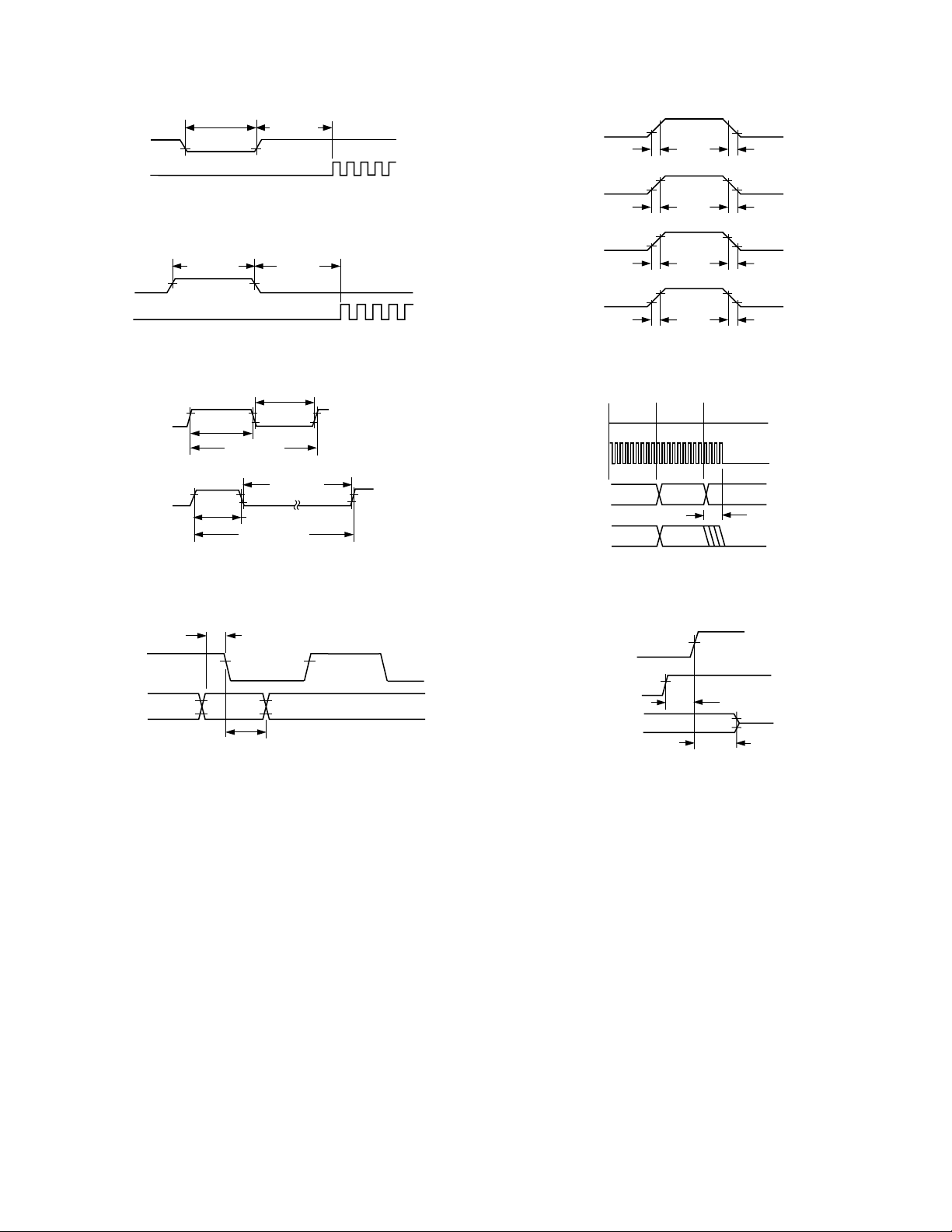
TIMING PARAMETERS (GUARANTEED OVER OPERATING TEMPERATURE RANGE)
Parameter Symbol Min Typ Max Unit
RESET Active Low Pulsewidth t
RESET Inactive to BIT_CLK Startup Delay t
SYNC Active High Pulsewidth t
SYNC Low Pulsewidth t
SYNC Inactive to BIT_CLK Startup Delay t
RST_LOW
RST2CLK
SYNC_HIGH
SYNC_LOW
SYNC2CLK
162.8 ns
162.8 ns
BIT_CLK Frequency 12.288 MHz
BIT_CLK Period t
CLK_PERIOD
BIT_CLK Output Jitter* 750 ps
BIT_CLK High Pulsewidth t
BIT_CLK Low Pulsewidth t
CLK_HIGH
CLK_LOW
32.56 42 48.84 ns
32.56 38 48.84 ns
SYNC Frequency 48.0 kHz
SYNC Period t
Setup to Falling Edge of BIT_CLK t
Hold from Falling Edge of BIT_CLK t
BIT_CLK Rise Time t
BIT_CLK Fall Time t
SYNC Rise Time t
SYNC Fall Time t
SDATA_IN Rise Time t
SDATA_IN Fall Time t
SDATA_OUT Rise Time t
SDATA_OUT Fall Time t
End of Slot 2 to BIT_CLK, SDATA_IN Low t
Setup to Trailing Edge of RESET (Applies to SYNC, SDATA_OUT) t
Rising Edge of RESET to HI-Z Delay t
SYNC_PERIOD
SETUP
HOLD
RISECLK
FALLCLK
RISESYNC
FALLSYNC
RISEDIN
FALLDIN
RISEDOUT
FALLDOUT
S2_PDOWN
SETUP2RST
OFF
5 2.5 ns
5ns
246 ns
246 ns
246 ns
246 ns
246 ns
246 ns
246 ns
246 ns
0 1.0 µs
15 ns
Propagation Delay 15 ns
RESET Rise Time 50 ns
Output Valid Delay from Rising Edge of BIT_CLK to SDI Valid 15 ns
*Guaranteed but not tested.
Specifications subject to change without notice.
1.0 µs
1.3 ms
19.5 µs
81.4 ns
20.8 µs
25 ns
REV. 0
–5–

AD1886A
RESET
BIT_CLK
SYNC
BIT_CLK
t
RST_LOW
t
RST2CLK
Figure 1. Cold Reset
t
SYNC_HIGH
t
RST2CLK
BIT_CLK
SYNC
SDATA_IN
SDATA_OUT
t
RISECLK
t
RISESYNC
t
RISEDIN
t
RISEDOUT
t
FALLCLK
t
FALLSYNC
t
FALLDIN
t
FALLDOUT
BIT_CLK
SYNC
SDATA_OUT
Figure 2. Warm Reset
t
CLK_LOW
BIT_CLK
SYNC
t
CLK_HIGH
t
CLK_PERIOD
t
SYNC_HIGH
t
SYNC_PERIOD
t
SYNC_LOW
Figure 3. Clock Timing
t
SETUP
t
HOLD
Figure 4. Data Setup and Hold
Figure 5. Signal Rise and Fall Time
WRITE
SLOT 2
DATA
PR4
DON’T
CARE
t
S2_PDOWN
SYNC
BIT_CLK
SDATA_OUT
SDATA_IN
SLOT 1
TO 0x26
NOTE: BIT_CLK NOT TO SCALE
Figure 6. AC Link Low Power Mode Timing
RESET
SDATA_OUT
SDATA_IN, BIT_CLK
t
OFF
t
SETUP2RST
HI-Z
Figure 7. ATE Test Mode
–6–
REV. 0

AD1886A
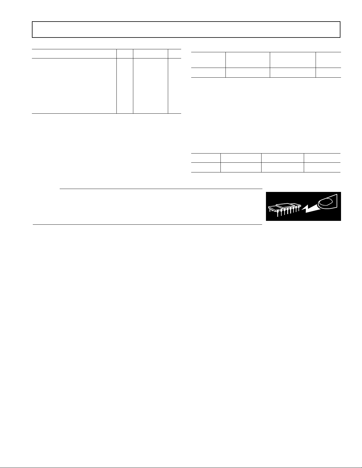
ABSOLUTE MAXIMUM RATINGS*
Parameter Min Max Unit
Power Supplies
Digital (DV
Analog (AV
) –0.3 +3.6 V
DD
) –0.3 +6.0 V
CC
Input Current (Except Supply Pins) ± 10.0 mA
Analog Input Voltage (Signal Pins) –0.3 AV
Digital Input Voltage (Signal Pins) –0.3 DV
+ 0.3 V
DD
+ 0.3 V
DD
Ambient Temperature (Operating) 0 70 °C
Storage Temperature –65 +150 °C
*Stresses greater than those listed under Absolute Maximum Ratings may cause
permanent damage to the device. This is a stress rating only; functional operation
of the device at these or any other conditions above those indicated in the
operational section of this specification is not implied. Exposure to absolute
maximum rating conditions for extended periods may affect device reliability.
Model Range Description Option*
AD1886AJST 0°C to 70°C 48-Lead LQFP ST-48
*ST = Thin Quad Flatpack.
ENVIRONMENTAL CONDITIONS
Ambient Temperature Rating
= T
T
T
P
θ
θ
θ
AMB
CASE
D
CA
JA
JC
CASE
= Case Temperature in °C
= Power Dissipation in W
= Thermal Resistance (Case-to-Ambient)
= Thermal Resistance (Junction-to-Ambient)
= Thermal Resistance (Junction-to-Case)
Package
ORDERING GUIDE
Temperature Package Package
– (PD × θCA)
JA
LQFP 76.2°C/W 17°C/W 59.2°C/W
CAUTION
ESD (electrostatic discharge) sensitive device. Electrostatic charges as high as 4000 V readily
accumulate on the human body and test equipment and can discharge without detection. Although
the AD1886A features proprietary ESD protection circuitry, permanent damage may occur on
devices subjected to high-energy electrostatic discharges. Therefore, proper ESD precautions are
recommended to avoid performance degradation or loss of functionality.
JC
WARNING!
CA
ESD SENSITIVE DEVICE
REV. 0
–7–

AD1886A
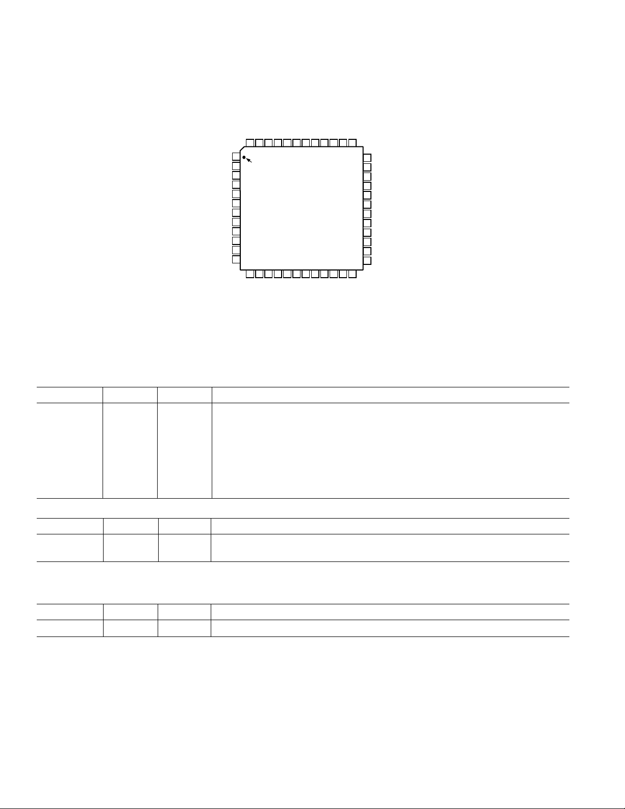
PIN CONFIGURATION
DV
DD1
XTL_IN
XTL_OUT
DV
SS1
SDATA_OUT
BIT_CLK
DV
SS2
SDATA_IN
DV
DD2
SYNC
RESET
PC_BEEP
AUX _L
AUX _R
SS3AVDD3
ID0
AV
AD1886A
TOP VIEW
(Not to Scale)
VIDEO_L
VIDEO_R
SPDIFJSID1
48 47 46 45 44 39 38 3743 42 41 40
1
PIN 1
2
IDENTIFIER
3
4
5
6
7
8
9
10
11
12
13 14 15 16 17 18 19 20 21 22 23 24
PHONE_IN
NC = NO CONNECT
NC
HP_OUT_R
CD_L
CD_R
CD_GND_REF
SS2
AV
HP_OUT_L
MIC1
MIC2
DD2
MONO_OUT
AV
36
35
34
33
32
31
30
29
28
27
26
25
LINE_IN_L
LINE_IN_R
LINE_OUT_R
LINE_OUT_L
CX3D
RX3D
FILT_L
FILT_R
AFILT2
AFILT1
V
REFOUT
V
REF
AV
SS1
AV
DD1
PIN FUNCTION DESCRIPTIONS
Digital I/O
Pin Name LQFP I/O Description
XTL_IN 2 I Crystal (or Clock) Input, 24.576 MHz.
XTL_OUT 3 O Crystal Output
SDATA_OUT 5 I AC-Link Serial Data Output, AD1886A Input Stream.
BIT_CLK 6 O/I AC-Link Bit Clock. 12.288 MHz Serial Data Clock. Daisy-Chain Output Clock.
SDATA_IN 8 O AC-Link Serial Data Input. AD1886A Output Stream.
SYNC 10 I AC-Link Frame Sync
RESET 11 I AC-Link Reset. AD1886A Master H/W Reset.
SPDIF 48 O SPDIF Output
CHIP SELECTS
Pin Name LQFP Type Description
ID0 45 I Chip Select Input 0 (Active Low)
ID1 46 I Chip Select Input 1 (Active Low)
JACK SENSE/GENERAL-PURPOSE DIGITAL OUTPUT
The JS pin can be used to sense the presence of an audio plug in the output jacks and automatically mute the MONO and/or
LINE_OUT audio outputs. Alternatively, the JS can be programmed as a general-purpose digital output pin.
Pin Name LQFP Type Description
JS 47 I/O JACK SENSE Input, or GPIO.
–8–
REV. 0

AD1886A
Analog I/O
These signals connect the AD1886A component to analog sources and sinks, including microphones and speakers.
Pin Name LQFP I/O Description
PC_BEEP 12 I PC Beep. PC Speaker beep passthrough.
PHONE 13 I Phone. From telephony subsystem speakerphone or handset.
AUX_L 14 I Auxiliary Input Left Channel
AUX_R 15 I Auxiliary Input Right Channel
VIDEO_L 16 I Video Audio Left Channel
VIDEO_R 17 I Video Audio Right Channel
CD_L 18 I CD Audio Left Channel
CD_GND_REF 19 I CD Audio Analog Ground Reference for CD Input
CD_ R 20 I CD Audio Right Channel
MIC1 21 I Microphone 1. Desktop microphone input.
MIC2 22 I Microphone 2. Second microphone input.
LINE_IN_L 23 I Line In, Left Channel.
LINE_IN_R 24 I Line In, Right Channel.
LINE_OUT_L 35 O Line Out, Left Channel.
LINE_OUT_R 36 O Line Out, Right Channel.
MONO_OUT 37 O Monaural Output to Telephony Subsystem Speakerphone
HP_OUT_L 39 O Headphones Out, Left Channel.
HP_OUT_R 41 O Headphones Out, Right Channel.
Filter/Reference
These signals are connected to resistors, capacitors, or specific voltages.
Pin Name LQFP I/O Description
V
REF
V
REFOUT
AFILT1 29 O Antialiasing Filter Capacitor—ADC Right Channel.
AFLIT2 30 O Antialiasing Filter Capacitor—ADC Left Channel.
FILT_R 31 O AC-Coupling Filter Capacitor—ADC Right Channel.
FILT_L 32 O AC-Coupling Filter Capacitor—ADC Left Channel.
RX3D 33 O 3D Phat Stereo Enhancement—Resistor.
CX3D 34 I 3D Phat Stereo Enhancement—Capacitor.
27 O Voltage Reference Filter
28 O Voltage Reference Output 5 mA Drive. (Intended for Mic Bias.)
Power and Ground Signals
Pin Name LQFP Type Description
1 1 I Digital VDD 3.3 V
DV
DD
DV
1 4 I Digital GND
SS
2 7 I Digital GND
DV
SS
DV
2 9 I Digital VDD 3.3 V
DD
AV
1 2 5 I Analog VDD 5.0 V
DD
1 26 I Analog GND
AV
SS
AV
2 3 8 I Analog VDD 5.0 V
DD
AV
2 40 I Analog GND
SS
3 4 3 I Analog VDD 5.0 V
AV
DD
AVSS3 44 I Analog GND
No Connects
Pin Name LQFP Type Description
NC 42 No Connect
REV. 0
–9–
 Loading...