

a
AC’97 SoundMAX® Codec
AD1886A
AC’97 2.1 FEATURES
Variable Sample Rate Audio
Multiple Codec Configuration Options
External Audio Power-Down Control
AC’97 FEATURES
AC’97 2.2 Compliant
Greater than 90 dB Dynamic Range
Stereo Headphone Amplifier
Multibit ⌺-⌬ Converter Architecture for Improved S/N
Ratio Greater than 90 dB
16-Bit Stereo Full-Duplex Codec
Four Analog Line-Level Stereo Inputs for:
LINE-IN, CD, VIDEO, and AUX
Two Analog Line-Level Mono Inputs for Speakerphone
and PC BEEP
Mono MIC Input w/Built-In 20 dB Preamp, Switchable
from Two External Sources
High-Quality CD Input with Ground Sense
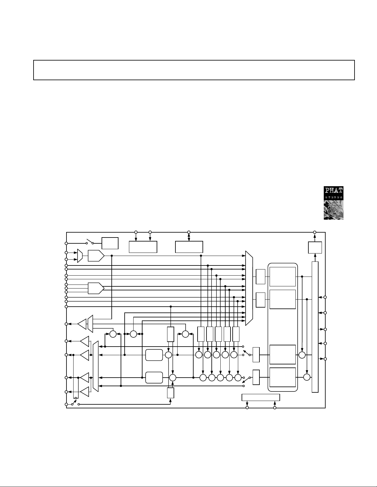
FUNCTIONAL BLOCK DIAGRAM
ID1
ID0
0dB/
20dB
VREF
CHIP SELECT
⌺
⌺
PHAT
STEREO
G
A
M
⌺
PHONE_IN
MONO_OUT
HP_OUT_L
LINE_OUT_L
V
REFOUT
VIDEO
MIC1
MIC2
LINE
AUX
CD
MV
MV
MV
JS
JACK SENSE
⌺
Stereo Line Level Outputs
Mono Output for Speakerphone or Internal Speaker
Power Management Support
48-Terminal LQFP Package
ENHANCED FEATURES
20-Bit SPDIF Output w/32 kHz, 44.1 kHz, and 48 kHz
Symbol Rates
Full Duplex Variable Sample Rates from 7040 Hz to
48 kHz with 1 Hz Resolution
Jack Sense Pins Provide Automatic Output Switching
Software-Enabled V
Output for Microphones and
REFOUT
External Power Amp
Split Power Supplies (3.3 V Digital/5 V Analog)
Mobile Low-Power Mixer Mode
Extended 6-Bit Master Volume Control
Extended 6-Bit Headphone Volume Control
Digital Audio Mixer Mode
Phat™ Stereo 3D Stereo Enhancement
SPDIF
G
G
A
A
M
M
⌺⌺⌺⌺
AD1886A
16-BIT
PGA
SELECTOR
PGA
G
G
G
A
A
A
M
M
M
G
⌺
⌺
A
M
⌺-⌬ A/D
CONVERTER
16-BIT
⌺-⌬ A/D
CONVERTER
SAMPLE
RATE
GENERATORS
16-BIT
⌺-⌬ D/A
CONVERTER
SPDIF
OUT
RESET
SYNC
BIT_CLK
AC LINK
SDATA_OUT
⌺
SDATA_IN
LINE_OUT_R
HP_OUT_R
PC_BEEP
MV
MV
PHAT
STEREO
⌺
A
M
G = GAIN
A = ATTENUATE
M = MUTE
SoundMAX is a registered trademark and Phat is a trademark of Analog Devices, Inc.
REV. 0
Information furnished by Analog Devices is believed to be accurate and
reliable. However, no responsibility is assumed by Analog Devices for its
use, nor for any infringements of patents or other rights of third parties that
may result from its use. No license is granted by implication or otherwise
under any patent or patent rights of Analog Devices.
One Technology Way, P.O. Box 9106, Norwood, MA 02062-9106, U.S.A.
Tel: 781/329-4700www.analog.com
Fax: 781/326-8703 © Analog Devices, Inc., 2001
⌺⌺ ⌺
⌺
⌺
XTAL_OUT
G
A
M
OSCILLATOR
XTAL_IN
16-BIT
⌺-⌬ D/A
CONVERTER
⌺

AD1886A–SPECIFICATIONS
STANDARD TEST CONDITIONS UNLESS OTHERWISE NOTED
Temperature 25°C
Digital Supply (V
Analog Supply (V
Sample Rate (f
) 3.3 V
DD
) 5.0 V
CC
) 48 kHz
S
Input Signal 1008 Hz
Analog Output Pass Band 20 Hz to 20 kHz
V
IH
V
IL
V
(CS0, CS1, CHAIN_IN) 4.0 V
IH
V
IL
ANALOG INPUT
2.0 V
0.8 V
1.0 V
Parameter Min Typ Max Unit
Input Voltage (RMS Values Assume Sine Wave Input)
LINE_IN, AUX, CD, VIDEO, PHONE_IN, PC_BEEP 1 V rms
MIC1 or MIC2 with +20 dB Gain (M20 = 1) 0.1 V rms
MIC1 or MIC2 with 0 dB Gain (M20 = 0) 1 V rms
Input Impedance* 20 kΩ
Input Capacitance* 5 7.5 pF
DAC Test Conditions
Calibrated
–3 dB Attenuation Relative to Full Scale
Input 0 dB
10 kΩ Output Load (LINE_OUT)
32 Ω Output Load (HP_OUT)
ADC Test Conditions
Calibrated
0 dB Gain
Input –3.0 dB Relative to Full Scale
2.83 V p-p
0.283 V p-p
2.83 V p-p
MASTER VOLUME
Parameter Min Typ Max Unit
Step Size (0 dB to –94.5 dB); LINE_OUT_L, LINE_OUT_R 1.5 dB
Output Attenuation Range Span* –94.5 dB
Step Size (0 dB to –46.5 dB); MONO_OUT 1.5 dB
Output Attenuation Range Span* –46.5 dB
Step Size (+6 dB to –88.5 dB); HP_OUT_R, HP_OUT_L 1.5 dB
Output Attenuation Range Span* –94.5 dB
Mute Attenuation of 0 dB Fundamental* 80 dB
PROGRAMMABLE GAIN AMPLIFIER—ADC
Parameter Min Typ Max Unit
Step Size (0 dB to 22.5 dB) 1.5 dB
PGA Gain Range Span 22.5 dB
ANALOG MIXER—INPUT GAIN / AMPLIFIERS / ATTENUATORS
Parameter Min Typ Max Unit
Signal-to-Noise Ratio (SNR)
CD to LINE_OUT 90 dB
Other to LINE_OUT 90 dB
Step Size (+12 dB to –34.5 dB): (All Steps Tested)
MIC, LINE_IN, AUX, CD, VIDEO, PHONE_IN, DAC 1.5 dB
Input Gain/Attenuation Range:
MIC, LINE, AUX, CD, VIDEO, PHONE_IN, DAC –46.5 dB
Step Size (0 dB to –45 dB): (All Steps Tested)
PC_BEEP 3.0 dB
Input Gain/Attenuation Range: PC_BEEP –45 dB
*Guaranteed but not tested.
–2–
REV. 0

AD1886A
DIGITAL DECIMATION AND INTERPOLATION FILTERS*
Parameter Min Typ Max Unit
Pass Band 0 0.4 × f
Pass-Band Ripple ± 0.09 dB
Transition Band 0.4 × f
Stop Band 0.6 × f
S
S
0.6 × f
∞ Hz
Stop-Band Rejection –74 dB
Group Delay 12/f
S
Group Delay Variation over Pass Band 0.0 µs
ANALOG-TO-DIGITAL CONVERTERS
Parameter Min Typ Max Unit
Resolution 16 Bits
Total Harmonic Distortion (THD) –84 dB
Dynamic Range (–60 dB input THD + N Referenced to Full Scale, A-Weighted) 84 87 dB
Signal-to-Intermodulation Distortion* (CCIF Method) 85 dB
ADC Crosstalk*
Line Inputs (Input L, Ground R, Read R; Input R, Ground L, Read L) –100 –90 dB
LINE_IN to Other –90 –85 dB
Gain Error (Full-Scale Span Relative to Nominal Input Voltage) ± 10 %
Interchannel Gain Mismatch (Difference of Gain Errors) ± 0.5 dB
ADC Offset Error ± 5mV
Hz
S
Hz
S
sec
DIGITAL-TO-ANALOG CONVERTERS
Parameter Min Typ Max Unit
Resolution 16 Bits
Total Harmonic Distortion (THD) LINE_OUT –85 dB
Total Harmonic Distortion (THD) HP_OUT –75 dB
Dynamic Range (–60 dB Input THD + N Referenced to Full Scale, A-Weighted) 85 90 dB
Signal-to-Intermodulation Distortion* (CCIF Method) –100 dB
Gain Error (Full-Scale Span Relative to Nominal Input Voltage) ± 10 %
Interchannel Gain Mismatch (Difference of Gain Errors) ± 0.7 dB
DAC Crosstalk* (Input L, Zero R, Measure R_OUT; Input R, Zero L, –80 dB
Measure L_OUT)
Total Audible Out-of-Band Energy (Measured from 0.6 × fS to 20 kHz)* –40 dB
ANALOG OUTPUT
Parameter Min Typ Max Unit
Full-Scale Output Voltage; LINE_OUT 1 V rms
2.83 V p-p
Output Impedance* 800 Ω
External Load Impedance* 10 kΩ
Output Capacitance* 15 pF
External Load Capacitance 100 pF
Full-Scale Output Voltage; HP_OUT (0 dB Gain) 1 V rms
Output Capacitance* 100 pF
External Load Impedance* 32 Ω
V
REF
V
REF_OUT
V
REF _OUT
Current Drive 5mA
2.05 2.25 2.45 V
2.25 V
Mute Click (Muted Output Minus Unmuted Midscale DAC Output) ± 5mV
*Guaranteed but not tested.
REV. 0
–3–

AD1886A–SPECIFICATIONS
STATIC DIGITAL SPECIFICATIONS
Parameter Min Typ Max Unit
High-Level Input Voltage (V
Low-Level Input Voltage (V
High-Level Output Voltage (V
Low-Level Output Voltage (V
Input Leakage Current –10 +10 µA
Output Leakage Current –10 +10 µA
POWER SUPPLY
Parameter Min Typ Max Unit
Power Supply Range—Analog (AV
Power Supply Range—Digital (DV
Power Dissipation—5 V/3.3 V 306 mW
Analog Supply Current—5 V (AV
Digital Supply Current—3.3 V (DV
Power Supply Rejection (100 mV p-p Signal @ 1 kHz)* 40 dB
(At Both Analog and Digital Supply Pins, Both ADCs and DACs)
CLOCK SPECIFICATIONS*
Parameter Min Typ Max Unit
Input Clock Frequency 24.576 MHz
Recommended Clock Duty Cycle 40 50 60 %
): Digital Inputs 0.65 × DV
IH
) 0.35 × DV
IL
), IOH = 2 mA 0.9 × DV
OH
), IOL = 2 mA 0.1 × DV
OL
) 4.75 5.0 5.25 V
DD
) 3.0 3.3 3.6 V
DD
)48mA
DD
)20mA
DD
DD
DD
DD
DD
V
V
V
V
POWER-DOWN STATES
Parameter Set Bits DVDD Typ AVDD Typ Unit
ADC PR0 17.5 41.6 mA
DAC PR1 17.0 38.3 mA
ADC + DAC PR1, PR0 4.1 31.9 mA
ADC + DAC + Mixer (Analog CD On) LPMIX, PR1, PR0 4.1 22.4 mA
Mixer PR2 20 17.5 mA
ADC + Mixer PR2, PR0 17.6 11.2 mA
DAC + Mixer PR2, PR1 17 8.4 mA
ADC + DAC + Mixer PR2, PR1, PR0 4.1 2.2 mA
Analog CD Only (AC-Link On) LPMIX, PR5, PR1, PR0 4.1 22.4 mA
Analog CD Only (AC-Link Off) LPMIX, PR1, PR0, PR4, PR5 0 22.4 mA
Standby PR5, PR4, PR3, PR2, PR1, PR0 0 0 mA
Headphone Standby PR6 20 38.8 mA
*Guaranteed but not tested.
Specifications subject to change without notice.
–4–
REV. 0

AD1886A
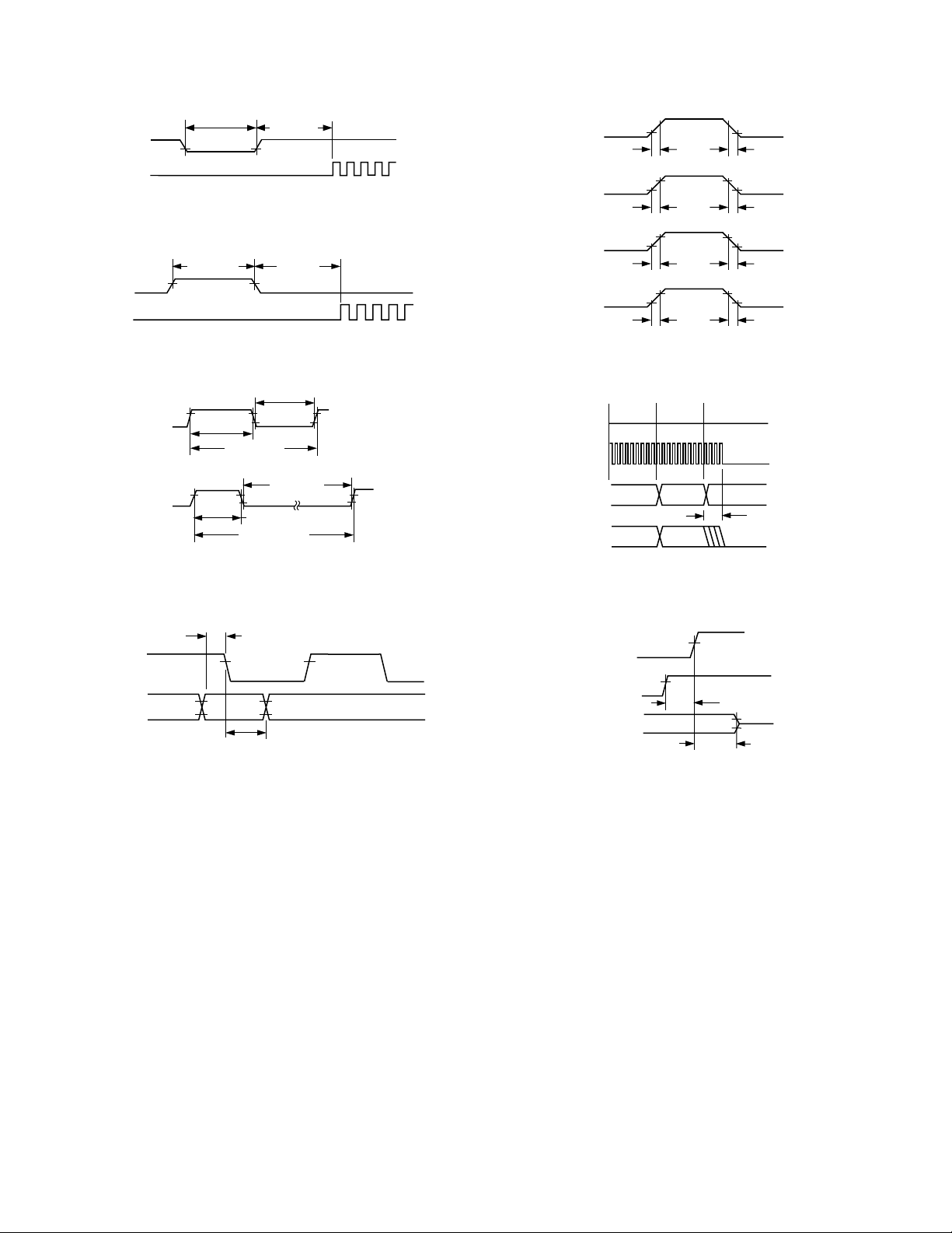
TIMING PARAMETERS (GUARANTEED OVER OPERATING TEMPERATURE RANGE)
Parameter Symbol Min Typ Max Unit
RESET Active Low Pulsewidth t
RESET Inactive to BIT_CLK Startup Delay t
SYNC Active High Pulsewidth t
SYNC Low Pulsewidth t
SYNC Inactive to BIT_CLK Startup Delay t
RST_LOW
RST2CLK
SYNC_HIGH
SYNC_LOW
SYNC2CLK
162.8 ns
162.8 ns
BIT_CLK Frequency 12.288 MHz
BIT_CLK Period t
CLK_PERIOD
BIT_CLK Output Jitter* 750 ps
BIT_CLK High Pulsewidth t
BIT_CLK Low Pulsewidth t
CLK_HIGH
CLK_LOW
32.56 42 48.84 ns
32.56 38 48.84 ns
SYNC Frequency 48.0 kHz
SYNC Period t
Setup to Falling Edge of BIT_CLK t
Hold from Falling Edge of BIT_CLK t
BIT_CLK Rise Time t
BIT_CLK Fall Time t
SYNC Rise Time t
SYNC Fall Time t
SDATA_IN Rise Time t
SDATA_IN Fall Time t
SDATA_OUT Rise Time t
SDATA_OUT Fall Time t
End of Slot 2 to BIT_CLK, SDATA_IN Low t
Setup to Trailing Edge of RESET (Applies to SYNC, SDATA_OUT) t
Rising Edge of RESET to HI-Z Delay t
SYNC_PERIOD
SETUP
HOLD
RISECLK
FALLCLK
RISESYNC
FALLSYNC
RISEDIN
FALLDIN
RISEDOUT
FALLDOUT
S2_PDOWN
SETUP2RST
OFF
5 2.5 ns
5ns
246 ns
246 ns
246 ns
246 ns
246 ns
246 ns
246 ns
246 ns
0 1.0 µs
15 ns
Propagation Delay 15 ns
RESET Rise Time 50 ns
Output Valid Delay from Rising Edge of BIT_CLK to SDI Valid 15 ns
*Guaranteed but not tested.
Specifications subject to change without notice.
1.0 µs
1.3 ms
19.5 µs
81.4 ns
20.8 µs
25 ns
REV. 0
–5–
AD1886A
RESET
BIT_CLK
SYNC
BIT_CLK
t
RST_LOW
t
RST2CLK
Figure 1. Cold Reset
t
SYNC_HIGH
t
RST2CLK
BIT_CLK
SYNC
SDATA_IN
SDATA_OUT
t
RISECLK
t
RISESYNC
t
RISEDIN
t
RISEDOUT
t
FALLCLK
t
FALLSYNC
t
FALLDIN
t
FALLDOUT
BIT_CLK
SYNC
SDATA_OUT
Figure 2. Warm Reset
t
CLK_LOW
BIT_CLK
SYNC
t
CLK_HIGH
t
CLK_PERIOD
t
SYNC_HIGH
t
SYNC_PERIOD
t
SYNC_LOW
Figure 3. Clock Timing
t
SETUP
t
HOLD
Figure 4. Data Setup and Hold
Figure 5. Signal Rise and Fall Time
WRITE
SLOT 2
DATA
PR4
DON’T
CARE
t
S2_PDOWN
SYNC
BIT_CLK
SDATA_OUT
SDATA_IN
SLOT 1
TO 0x26
NOTE: BIT_CLK NOT TO SCALE
Figure 6. AC Link Low Power Mode Timing
RESET
SDATA_OUT
SDATA_IN, BIT_CLK
t
OFF
t
SETUP2RST
HI-Z
Figure 7. ATE Test Mode
–6–
REV. 0

AD1886A
ABSOLUTE MAXIMUM RATINGS*
Parameter Min Max Unit
Power Supplies
Digital (DV
Analog (AV
) –0.3 +3.6 V
DD
) –0.3 +6.0 V
CC
Input Current (Except Supply Pins) ± 10.0 mA
Analog Input Voltage (Signal Pins) –0.3 AV
Digital Input Voltage (Signal Pins) –0.3 DV
+ 0.3 V
DD
+ 0.3 V
DD
Ambient Temperature (Operating) 0 70 °C
Storage Temperature –65 +150 °C
*Stresses greater than those listed under Absolute Maximum Ratings may cause
permanent damage to the device. This is a stress rating only; functional operation
of the device at these or any other conditions above those indicated in the
operational section of this specification is not implied. Exposure to absolute
maximum rating conditions for extended periods may affect device reliability.
Model Range Description Option*
AD1886AJST 0°C to 70°C 48-Lead LQFP ST-48
*ST = Thin Quad Flatpack.
ENVIRONMENTAL CONDITIONS
Ambient Temperature Rating
= T
T
T
P
θ
θ
θ
AMB
CASE
D
CA
JA
JC
CASE
= Case Temperature in °C
= Power Dissipation in W
= Thermal Resistance (Case-to-Ambient)
= Thermal Resistance (Junction-to-Ambient)
= Thermal Resistance (Junction-to-Case)
Package
ORDERING GUIDE
Temperature Package Package
– (PD × θCA)
JA
LQFP 76.2°C/W 17°C/W 59.2°C/W
CAUTION
ESD (electrostatic discharge) sensitive device. Electrostatic charges as high as 4000 V readily
accumulate on the human body and test equipment and can discharge without detection. Although
the AD1886A features proprietary ESD protection circuitry, permanent damage may occur on
devices subjected to high-energy electrostatic discharges. Therefore, proper ESD precautions are
recommended to avoid performance degradation or loss of functionality.
JC
WARNING!
CA
ESD SENSITIVE DEVICE
REV. 0
–7–
AD1886A
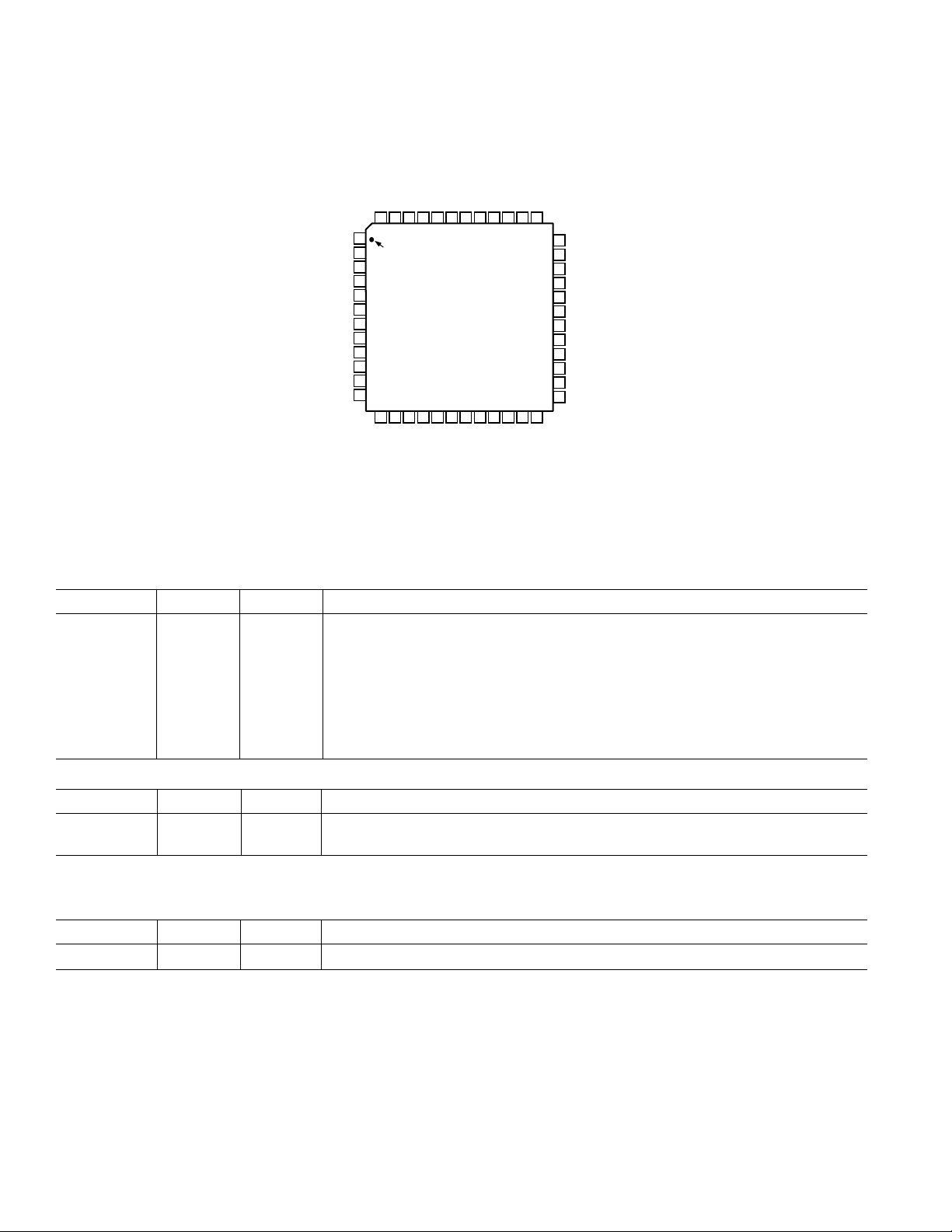
PIN CONFIGURATION
DV
DD1
XTL_IN
XTL_OUT
DV
SS1
SDATA_OUT
BIT_CLK
DV
SS2
SDATA_IN
DV
DD2
SYNC
RESET
PC_BEEP
AUX _L
AUX _R
SS3AVDD3
ID0
AV
AD1886A
TOP VIEW
(Not to Scale)
VIDEO_L
VIDEO_R
SPDIFJSID1
48 47 46 45 44 39 38 3743 42 41 40
1
PIN 1
2
IDENTIFIER
3
4
5
6
7
8
9
10
11
12
13 14 15 16 17 18 19 20 21 22 23 24
PHONE_IN
NC = NO CONNECT
NC
HP_OUT_R
CD_L
CD_R
CD_GND_REF
SS2
AV
HP_OUT_L
MIC1
MIC2
DD2
MONO_OUT
AV
36
35
34
33
32
31
30
29
28
27
26
25
LINE_IN_L
LINE_IN_R
LINE_OUT_R
LINE_OUT_L
CX3D
RX3D
FILT_L
FILT_R
AFILT2
AFILT1
V
REFOUT
V
REF
AV
SS1
AV
DD1
PIN FUNCTION DESCRIPTIONS
Digital I/O
Pin Name LQFP I/O Description
XTL_IN 2 I Crystal (or Clock) Input, 24.576 MHz.
XTL_OUT 3 O Crystal Output
SDATA_OUT 5 I AC-Link Serial Data Output, AD1886A Input Stream.
BIT_CLK 6 O/I AC-Link Bit Clock. 12.288 MHz Serial Data Clock. Daisy-Chain Output Clock.
SDATA_IN 8 O AC-Link Serial Data Input. AD1886A Output Stream.
SYNC 10 I AC-Link Frame Sync
RESET 11 I AC-Link Reset. AD1886A Master H/W Reset.
SPDIF 48 O SPDIF Output
CHIP SELECTS
Pin Name LQFP Type Description
ID0 45 I Chip Select Input 0 (Active Low)
ID1 46 I Chip Select Input 1 (Active Low)
JACK SENSE/GENERAL-PURPOSE DIGITAL OUTPUT
The JS pin can be used to sense the presence of an audio plug in the output jacks and automatically mute the MONO and/or
LINE_OUT audio outputs. Alternatively, the JS can be programmed as a general-purpose digital output pin.
Pin Name LQFP Type Description
JS 47 I/O JACK SENSE Input, or GPIO.
–8–
REV. 0

AD1886A
Analog I/O
These signals connect the AD1886A component to analog sources and sinks, including microphones and speakers.
Pin Name LQFP I/O Description
PC_BEEP 12 I PC Beep. PC Speaker beep passthrough.
PHONE 13 I Phone. From telephony subsystem speakerphone or handset.
AUX_L 14 I Auxiliary Input Left Channel
AUX_R 15 I Auxiliary Input Right Channel
VIDEO_L 16 I Video Audio Left Channel
VIDEO_R 17 I Video Audio Right Channel
CD_L 18 I CD Audio Left Channel
CD_GND_REF 19 I CD Audio Analog Ground Reference for CD Input
CD_ R 20 I CD Audio Right Channel
MIC1 21 I Microphone 1. Desktop microphone input.
MIC2 22 I Microphone 2. Second microphone input.
LINE_IN_L 23 I Line In, Left Channel.
LINE_IN_R 24 I Line In, Right Channel.
LINE_OUT_L 35 O Line Out, Left Channel.
LINE_OUT_R 36 O Line Out, Right Channel.
MONO_OUT 37 O Monaural Output to Telephony Subsystem Speakerphone
HP_OUT_L 39 O Headphones Out, Left Channel.
HP_OUT_R 41 O Headphones Out, Right Channel.
Filter/Reference
These signals are connected to resistors, capacitors, or specific voltages.
Pin Name LQFP I/O Description
V
REF
V
REFOUT
AFILT1 29 O Antialiasing Filter Capacitor—ADC Right Channel.
AFLIT2 30 O Antialiasing Filter Capacitor—ADC Left Channel.
FILT_R 31 O AC-Coupling Filter Capacitor—ADC Right Channel.
FILT_L 32 O AC-Coupling Filter Capacitor—ADC Left Channel.
RX3D 33 O 3D Phat Stereo Enhancement—Resistor.
CX3D 34 I 3D Phat Stereo Enhancement—Capacitor.
27 O Voltage Reference Filter
28 O Voltage Reference Output 5 mA Drive. (Intended for Mic Bias.)
Power and Ground Signals
Pin Name LQFP Type Description
1 1 I Digital VDD 3.3 V
DV
DD
DV
1 4 I Digital GND
SS
2 7 I Digital GND
DV
SS
DV
2 9 I Digital VDD 3.3 V
DD
AV
1 2 5 I Analog VDD 5.0 V
DD
1 26 I Analog GND
AV
SS
AV
2 3 8 I Analog VDD 5.0 V
DD
AV
2 40 I Analog GND
SS
3 4 3 I Analog VDD 5.0 V
AV
DD
AVSS3 44 I Analog GND
No Connects
Pin Name LQFP Type Description
NC 42 No Connect
REV. 0
–9–

AD1886A
SPDIFJS
MIC1
MIC2
LINE_IN
AUX
VIDEO
PHONE_IN
HP_OUT_L
LINE_OUT_L
MONO_OUT
LINE_OUT_R
HP_OUT_R
AD1886A
0
0dB/20dB
MS
M20 0x0E
1
S 0x20
CD
LS/RS (0)
LS (4)
RS (4)
GM 0x1C
LIM
LS (3)
IM
RS (3)
LS (1)
RS (1)
LS (2)
RS (2)
LS/RS (7)
GM 0x1C
RIM
LS (5)
IM
LS/RS (6)
RS (5)
S
E
L
E
C
T
O
R
GM 0x1C
LIV
IM
GM 0x1C
RIV
IM
JACK SENSE
0x72
16-BIT
⌺-⌬ A/D
16-BIT
⌺-⌬ A/D
SPDIF
0x3A
0x2A
0x28
0x72
RESET
S 0x1A
SYNC
BIT_CLK
AC LINK
SDATA_OUT
SDATA_IN
0x04
HPM
M 0x02
MM
M 0x06
MMM
M 0x02
MM
0x04
HPM
0x04
LHV
A 0x02
LMV
A 0x06
MMV
A 0x02
RMV
0x04
RHV
MIX
0
1
S 0x20
⌺
D
A
M
GA 0x0C
PHV
M 0x0C
PHM
⌺
⌺
M 0x0A
PCM
3D 0x22
POP3D
3D 0x22
POP3D
⌺
GA 0x0E
MCV
M 0x0E
MCM
⌺
⌺
GA 0x10
LLV
RLA
M 0x10
LM
⌺
GA 0x12
LCV
RCV
M 0x12CMM 0x16
⌺
⌺
⌺
GA 0x16
LAV
RAV
AM
⌺
⌺
GA 0x14
LV V
RVV
M 0x14
VM
⌺
GAM 0x18
LOV
OM
3D 0x20
SWITCH
⌺
GAM 0x18
ROV
OM
16-BIT
⌺-⌬ D/A
16-BIT
⌺-⌬ D/A
⌺
⌺
PC_BEEP
A 0x0A
PCV
Figure 8. Block Diagram Register Map
OSCILLATORS
XTL_OUT XTL_IN
–10–
REV. 0

AD1886A
Indexed Control Registers
Reg
Num Name D15 D14 D13 D12 D11 D10 D9 D8 D7 D6 D5 D4 D3 D2 D1 D0 Default
00h Reset X SE4 SE3 SE2 SE1 SE0 ID9 ID8 ID7 ID6 ID5 ID4 ID3 ID2 ID1 ID0 0410h
02h Master Volume MM X LMV5 LMV4 LMV3 LMV2 LMV1 LMV0 X X RMV5 RMV4 RMV3 RMV2
04h Headphones Volume HPM X LHV5 LHV4 LHV3 LHV2 LHV1 LHV0 X X RHV5 RHV4 RHV3 RHV2 RHV1 RHV0 8000h
06h Master Volume Mono MMM XXXXXXXXXXMMV4
08h Reserved X XXXXXXXXXXX X X XX X
0Ah PC Beep Volume PCM XXXXXXXXXXPCV3 PCV2 PCV1 PCV0 X 8000h
0Ch Phone-In Volume PHM XXXXXXXXXXPHV4 PHV3 PHV2 PHV1 PHV0 8008h
0Eh Mic Volume MCM XXXXXXXXM20XMCV4MCV3
10h Line-In Volume LM X X LLV4 LLV3 LLV2 LLV1 LLV0 X X X RLV4 RLV3 RLV2 RLV1 RLV0 8808h
12h CD Volume CVM X X LCV4 LCV3 LCV2 LCV1 LCV0 X X X RCV4 RCV3 RCV2 RCV1 RCV0 8808h
14h Video Volume VM X X LVV4 LVV3 LVV2 LVV1 LVV0 X X X RVV4 RVV3 RVV2 RVV1 RVV0 8808h
16h Aux Volume AM X X LAV4 LAV3 LAV2 LAV1 LAV0 X X X RAV4 RAV3 RAV2 RAV1 RAV0 8808h
18h PCM Out Vol OM X X LOV4 LOV3 LOV2 LOV1 LOV0 X X X ROV4 ROV3 ROV2 ROV1 ROV0 8808h
1Ah Record Select X XXXXLS2LS1LS0XXXXXRS2RS1RS00000h
1Ch Record Gain IM X X X LIM3 LIM2 LIM1 LIM0 X X X X RIM3 RIM2 RIM1 RIM0 8000h
20h General-Purpose POP X 3D X X X MIX MS LPBK X X X X X X X 0000h
22h 3D Control X XXXXXXXXXXX DP3DP2DP1DP00000h
26h Power-Down Ctrl/Stat X X PR5 PR4 PR3 PR2 PR1 PR0 X X X X REF ANL DAC ADC 000Xh
28h Ext’d Audio ID ID1 ID0 X X X XXXXXXX X SPDF X VRA 0005h
2Ah Ext’d Audio Stat/Ctrl X XXXXSPCV X X X X SPSA1 SPSA0 X SPDIF X VRA 0000h
2Ch/ PCM DAC Rate (SR1) SR15 SR14 SR13 SR12 SR11 SR10 SR9 SR8 SR7 SR6 SR5 SR4 SR3 SR2 SR1 SR0 BB80h
(7Ah)*
32h/ PCM ADC Rate (SR0) SR15 SR14 SR13 SR12 SR11 SR10 SR9 SR8 SR7 SR6 SR5 SR4 SR3 SR2 SR1 SR0 BB80h
(78h)*
3Ah SPDIF Control V X SPSR1
72h Jack Sense/SPDIF SPMIX JSOD SPRZ JSPD X JSOE JSLM JSD X JSC JSMM JSM VWI JS1 JS0 JSI 0000h
74h Serial Configuration
76h Misc Control Bits DACZ
7Ch Vendor ID1 F7 F6 F5 F4 F3 F2 F1 F0 S7 S6 S5 S4 S3 S2 S1 S0 4144h
7Eh Vendor ID2 T7 T6 T5 T4 T3 T2 T1 T0 REV7 REV6 REV5 REV4 REV3 REV2 REV1 REV0 5363h
NOTES
All registers not shown and bits containing an X are assumed to be reserved.
Odd register addresses are aliased to the next lower even address.
Reserved registers should not be written.
Zeros should be written to reserved bits.
*Indicates Aliased register for AD1819, AD1819A backward compatibility
SLOT16 REGM2 REGM1 REGM0 DRQEN
LPMIX
SPSR0
L CC6 CC5 CC4 CC3 CC2 CC1 CC0 PRE COPY AUD PRO 0000h
XXXXXXX X XXX 7000h
X DAM DMS DLSR X ALSR MOD SRX1 SRX8 X X DRSR X ARSR 0404h
EN 0D7 D7
MMV3 MMV2 MMV1 MMV0
RMV1
RMV0 8000h
MCV2 MCV1 MCV0
8000h
8008h
REV. 0
–11–

AD1886A
Reset (Index 00h)
geRgeR
geRgeR
geR
muNmuN
muNmuN
muN
h00h00
h00h00teseRteseR
h00
Note: Writing any value to this register performs a register reset, which causes all registers to revert to their default values (except 74h,
which forces the serial configuration). Reading this register returns the ID code of the part and a code for the type of 3D Stereo
Enhancement.
ID[9:0] Identify Capability. The ID decodes the capabilities of AD1886A based on the following:
SE[4:0] Stereo Enhancement. The 3D stereo enhancement identifies the Analog Devices 3D stereo enhancement.
Master Volume Registers (Index 02h)
geRgeR
geRgeR
geR
muNmuN
muNmuNemaNemaN
muN
h20h20
h20h20
h20
emaNemaN
emaNemaN51D51D
emaN
teseRteseRXXXXX4ES4ES
teseR
emaNemaN51D51D
emaN
retsaMretsaM
retsaMretsaM
retsaM
51D51D41D41D
51D
51D51D41D41D
51D
emuloVemuloV
emuloVemuloVMMMMMMMMMMXXXXX5VML5VML
emuloV
41D41D31D31D
41D
4ES4ES3ES3ES
4ES
41D41D31D31D
41D
31D31D21D21D
21D21D11D11D
11D11D01D01D
31D
3ES3ES2ES2ES
3ES
21D
2ES2ES1ES1ES
2ES
01D01D9D9D9D9D9D8D8D8D8D8D7D7D7D7D7D6D6D6D6D6D5D5D5D5D5D4D4D4D4D4D3D3D3D3D3D2D2D2D2D2D1D1D1D1D1D0D0D0D0D0DtluafeDtluafeD
11D
01D
1ES1ES0ES0ES
0ES0ES9DI9DI
9DI9DI8DI8DI
8DI8DI7DI7DI
7DI7DI6DI6DI
6DI6DI5DI5DI
5DI5DI4DI4DI
1ES
0ES
9DI
8DI
7DI
6DI
4DI4DI3DI3DI
5DI
4DI
Bit = 1 Function AD1886A*
ID0 Dedicated Mic PCM in Channel 0
ID1 Modem Line Codec support 0
ID2 Bass and Treble Control 0
ID3 Simulated Stereo (Mono to Stereo) 0
ID4 Headphone Out Support 1
ID5 Loudness (Bass Boost) Support 0
ID6 18-Bit DAC Resolution 0
ID7 20-Bit DAC Resolution 0
ID8 18-Bit ADC Resolution 0
ID9 20-Bit ADC Resolution 0
*The AD1886A contains none of the optional features identified by these bits.
31D31D21D21D
21D21D11D11D
11D11D01D01D
31D
21D
5VML5VML4VML4VML
4VML4VML3VML3VML
5VML
4VML
01D01D9D9D9D9D9D8D8D8D8D8D7D7D7D7D7D6D6D6D6D6D5D5D5D5D5D4D4D4D4D4D3D3D3D3D3D2D2D2D2D2D1D1D1D1D1D0D0D0D0D0DtluafeDtluafeD
11D
01D
3VML3VML2VML2VML
2VML2VML1VML1VML
1VML1VML0VML0VML
3VML
2VML
0VML0VMLXXXXXXXXXX5VMR5VMR
1VML
0VML
5VMR5VMR4VMR4VMR
5VMR
4VMR4VMR3VMR3VMR
4VMR
3DI3DI2DI2DI
3DI
3VMR3VMR2VMR2VMR
3VMR
2DI2DI1DI1DI
2DI
2VMR2VMR1VMR1VMR
2VMR
1DI1DI0DI0DI
1DI
1VMR1VMR0VMR0VMR
1VMR
0DI0DIh0140h0140
0DI
0VMR0VMRh0008h0008
0VMR
tluafeDtluafeD
tluafeD
h0140h0140
h0140
tluafeDtluafeD
tluafeD
h0008h0008
h0008
RMV[5:0] Right Master Volume Control. The least significant bit represents 1.5 dB. This register controls the output from
0 dB to a maximum attenuation of –94.5 dB.
LMV[5:0] Left Master Volume Control. The least significant bit represents 1.5 dB. This register controls the output from
0 dB to a maximum attenuation of –94.5 dB.
MM Master Volume Mute. When this bit is set to “1,” the channel is muted.
MM xMV5 . . . xMV0 Function
0 00 0000 0 dB Attenuation
0 01 1111 –46.5 dB Attenuation
0 11 1111 –94.5 dB Attenuation
1 xx xxxx –∞ dB Attenuation
–12–
REV. 0

AD1886A
Headphones Volume Registers (Index 04h)
geRgeR
geRgeR
geR
muNmuN
muNmuNemaNemaN
muN
h40h40
h40h40emuloVenohpdaeHemuloVenohpdaeH
h40
RHV[5:0] Right Headphone Volume Control. The least significant bit represents 1.5 dB. This register controls the output
LHV[5:0] Left Headphone Volume Control. The least significant bit represents 1.5 dB. This register controls the output
HPM Headphones Volume Mute. When this bit is set to “1,” the channel is muted.
Master Volume Mono (Index 06h)
geRgeR
geRgeR
geR
muNmuN
muNmuNemaNemaN
muN
h60h60
h60h60
h60
MMV[5:0] Mono Master Volume Control. The least significant bit represents 1.5 dB. This register controls the output from
MMM Mono Master Volume Mute. When this bit is set to “1,” the channel is muted.
PC Beep Register (Index 0Ah)
geRgeR
geRgeR
geR
muNmuN
muNmuNemaNemaN
muN
hA0hA0
hA0hA0emuloVPEEB_CPemuloVPEEB_CP
hA0
emaNemaN51D51D
emaN
emuloVenohpdaeHemuloVenohpdaeHMPHMPH
emuloVenohpdaeH
51D51D41D41D
41D41D31D31D
51D
41D
MPHMPHXXXXX5VHL5VHL
MPH
31D31D21D21D
31D
5VHL5VHL4VHL4VHL
5VHL
21D21D11D11D
21D
4VHL4VHL3VHL3VHL
4VHL
11D11D01D01D
11D
from +6 dB to a maximum attenuation of –88.5 dB.
from +6 dB to a maximum attenuation of –88.5 dB.
HPM xHV5 . . . xHV0 Function
0 00 0000 6 dB Gain
0 01 1111 –40.5 dB Attenuation
0 11 1111 –88.5 dB Attenuation
1 xx xxxx –∞ dB Attenuation
emaNemaN51D51D
emaN
onoMonoM
onoMonoMMMMMMM
onoM
51D51D41D41D
41D41D31D31D
31D31D21D21D
21D21D11D11D
11D11D01D01D
51D
41D
31D
21D
emuloVretsaMemuloVretsaM
emuloVretsaMemuloVretsaM
emuloVretsaM
MMMMMMXXXXXXXXXXXXXXXXXXXXXXXXXXXXXXXXXXXXXXXXXXXXX5VMM5VMM
MMM
01D01D9D9D9D9D9D8D8D8D8D8D7D7D7D7D7D6D6D6D6D6D5D5D5D5D5D4D4D4D4D4D3D3D3D3D3D2D2D2D2D2D1D1D1D1D1D0D0D0D0D0DtluafeDtluafeD
11D
01D
0 dB to a maximum attenuation of –94.5 dB.
emaNemaN51D51D
emaN
51D51D41D41D
41D41D31D31D
31D31D21D21D
51D
41D
emuloVPEEB_CPemuloVPEEB_CPMCPMCP
MCPMCPXXXXXXXXXXXXXXXXXXXXXXXXXXXXXXXXXXXXXXXXXXXXXXXXXX3VCP3VCP
emuloVPEEB_CP
MCP
21D21D11D11D
31D
21D
01D01D9D9D9D9D9D8D8D8D8D8D7D7D7D7D7D6D6D6D6D6D5D5D5D5D5D4D4D4D4D4D3D3D3D3D3D2D2D2D2D2D1D1D1D1D1D0D0D0D0D0DtluafeDtluafeD
01D
3VHL3VHL2VHL2VHL
2VHL2VHL1VHL1VHL
1VHL1VHL0VHL0VHL
3VHL
2VHL
11D11D01D01D
01D01D9D9D9D9D9D8D8D8D8D8D7D7D7D7D7D6D6D6D6D6D5D5D5D5D5D4D4D4D4D4D3D3D3D3D3D2D2D2D2D2D1D1D1D1D1D0D0D0D0D0DtluafeDtluafeD
11D
01D
1VHL
0VHL0VHLXXXXXXXXXX5VHR5VHR
0VHL
5VMM5VMM4VMM4VMM
5VMM
5VHR5VHR4VHR4VHR
5VHR
4VMM4VMM3VMM3VMM
4VMM
4VHR4VHR3VHR3VHR
4VHR
3VCP3VCP2VCP2VCP
3VCP
3VMM3VMM2VMM2VMM
3VMM
3VHR3VHR2VHR2VHR
3VHR
2VCP2VCP1VCP1VCP
2VCP
2VHR2VHR1VHR1VHR
2VHR
2VMM2VMM1VMM1VMM
2VMM
1VCP1VCP0VCP0VCP
1VCP
1VHR1VHR0VHR0VHR
1VHR
1VMM1VMM0VMM0VMM
1VMM
0VCP0VCPXXXXXh0008h0008
0VCP
0VHR0VHRh0008h0008
0VHR
0VMM0VMMh0008h0008
0VMM
tluafeDtluafeD
tluafeD
h0008h0008
h0008
tluafeDtluafeD
tluafeD
h0008h0008
h0008
tluafeDtluafeD
tluafeD
h0008h0008
h0008
PCV[3:0] PC Beep Volume Control. The least significant bit represents 3 dB attenuation. This register controls the output
from 0 dB to a maximum attenuation of –45 dB. The PC Beep is routed to Left and Right Line outputs even when
AD1886A is in a RESET State. This is so Power-On Self-Test (POST) codes can be heard by the user in case of a
hardware problem with the PC.
PCM PC Beep Mute. When this bit is set to “1,” the channel is muted.
PCM PCV3 . . . PCV0 Function
0 0000 0 dB Attenuation
0 1111 45 dB Attenuation
1 xxxx ∞ dB Attenuation
REV. 0
–13–

AD1886A
Phone Volume (Index 0Ch)
geRgeR
geRgeR
geR
muNmuN
muNmuN
muN
hC0hC0
hC0hC0emuloVenohPemuloVenohP
hC0
PHV[4:0] Phone Volume. Allows setting the Phone Volume Attenuator in 32 steps. The LSB represents 1.5 dB, and the
PHM Phone Mute. When this bit is set to “1,” the channel is muted.
Mic Volume (Index 0Eh)
geRgeR
geRgeR
geR
muNmuN
muNmuN
muN
hE0hE0
hE0hE0
hE0
MCV[4:0] Mic Volume Gain. Allows setting the Mic Volume attenuator in 32 steps. The LSB represents 1.5 dB, and the
M20 Microphone 20 dB Gain Block
MCM Mic Mute. When this bit is set to “1,” the channel is muted.
Line In Volume (Index 10h)
geRgeR
geRgeR
geR
muNmuN
muNmuN
muN
h01h01
h01h01emuloVnIeniLemuloVnIeniL
h01
emaNemaN
emaNemaN51D51D
emaN
range is +12 dB to –34.5 dB. The default value is 0 dB, mute enabled.
emaNemaN
emaNemaN51D51D
emaN
CIMCIM
CIMCIM
CIM
emuloVemuloV
emuloVemuloV
emuloV
range is +12 dB to –34.5 dB. The default value is 0 dB, mute enabled.
0 = Disabled; Gain = 0 dB
1 = Enabled; Gain = 20 dB
emaNemaN
emaNemaN51D51D
emaN
51D51D41D41D
41D41D31D31D
31D31D21D21D
21D21D11D11D
11D11D01D01D
51D
41D
31D
21D
emuloVenohPemuloVenohPMHPMHP
MHPMHPXXXXXXXXXXXXXXXXXXXXXXXXXXXXXXXXXXXXXXXXXXXXXXXXXX4VHP4VHP
emuloVenohP
MHP
51D51D41D41D
41D41D31D31D
31D31D21D21D
21D21D11D11D
51D
41D
31D
MCMMCM
MCMMCMXXXXXXXXXXXXXXXXXXXXXXXXXXXXXXXXXXXXXXXX02M02M
MCM
51D51D41D41D
41D41D31D31D
51D
emuloVnIeniLemuloVnIeniLMLMLMLMLMLXXXXXXXXXX4VLL4VLL
emuloVnIeniL
31D31D21D21D
41D
31D
21D
21D21D11D11D
21D
4VLL4VLL3VLL3VLL
4VLL
11D11D01D01D
11D
11D11D01D01D
11D
3VLL3VLL2VLL2VLL
3VLL
01D01D9D9D9D9D9D8D8D8D8D8D7D7D7D7D7D6D6D6D6D6D5D5D5D5D5D4D4D4D4D4D3D3D3D3D3D2D2D2D2D2D1D1D1D1D1D0D0D0D0D0DtluafeDtluafeD
11D
01D
01D01D9D9D9D9D9D8D8D8D8D8D7D7D7D7D7D6D6D6D6D6D5D5D5D5D5D4D4D4D4D4D3D3D3D3D3D2D2D2D2D2D1D1D1D1D1D0D0D0D0D0DtluafeDtluafeD
01D
01D01D9D9D9D9D9D8D8D8D8D8D7D7D7D7D7D6D6D6D6D6D5D5D5D5D5D4D4D4D4D4D3D3D3D3D3D2D2D2D2D2D1D1D1D1D1D0D0D0D0D0DtluafeDtluafeD
01D
2VLL2VLL1VLL1VLL
1VLL1VLL0VLL0VLL
2VLL
0VLL0VLLXXXXXXXXXXXXXXX4VLR4VLR
1VLL
0VLL
02M02MXXXXX4VCM4VCM
02M
4VHP4VHP3VHP3VHP
4VHP
4VCM4VCM3VCM3VCM
4VCM
4VLR4VLR3VLR3VLR
4VLR
3VHP3VHP2VHP2VHP
3VHP
3VCM3VCM2VCM2VCM
3VCM
3VLR3VLR2VLR2VLR
3VLR
2VHP2VHP1VHP1VHP
2VHP
2VCM2VCM1VCM1VCM
2VCM
2VLR2VLR1VLR1VLR
2VLR
1VHP1VHP0VHP0VHP
1VHP
1VCM1VCM0VCM0VCM
1VCM
1VLR1VLR0VLR0VLR
1VLR
0VHP0VHPh8008h8008
0VHP
0VCM0VCMh8008h8008
0VCM
0VLR0VLRh8088h8088
0VLR
tluafeDtluafeD
tluafeD
h8008h8008
h8008
tluafeDtluafeD
tluafeD
h8008h8008
h8008
tluafeDtluafeD
tluafeD
h8088h8088
h8088
RLV[4:0] Right Line In Volume. Allows setting the Line In right channel attenuator in 32 steps. The LSB represents 1.5 dB,
and the range is +12 dB to –34.5 dB. The default value is 0 dB, mute enabled.
LLV[4:0] Left Line In Volume. Allows setting the Line In left channel attenuator in 32 steps. The LSB represents 1.5 dB,
and the range is +12 dB to –34.5 dB. The default value is 0 dB, mute enabled.
LM Line In Mute. When this bit is set to “1,” the channel is muted.
CD Volume (Index 12h)
geRgeR
geRgeR
geR
muNmuN
muNmuN
muN
h21h21
h21h21emuloVDCemuloVDC
h21
emaNemaN
emaNemaN51D51D
emaN
emuloVDCemuloVDCMVCMVC
emuloVDC
51D51D41D41D
41D41D31D31D
51D
MVCMVCXXXXXXXXXX4VCL4VCL
MVC
31D31D21D21D
41D
31D
21D21D11D11D
21D
4VCL4VCL3VCL3VCL
4VCL
11D11D01D01D
01D01D9D9D9D9D9D8D8D8D8D8D7D7D7D7D7D6D6D6D6D6D5D5D5D5D5D4D4D4D4D4D3D3D3D3D3D2D2D2D2D2D1D1D1D1D1D0D0D0D0D0DtluafeDtluafeD
11D
01D
3VCL3VCL2VCL2VCL
2VCL2VCL1VCL1VCL
1VCL1VCL0VCL0VCL
3VCL
2VCL
0VCL0VCLXXXXXXXXXXXXXXX4VCR4VCR
1VCL
0VCL
4VCR4VCR3VCR3VCR
4VCR
3VCR3VCR2VCR2VCR
3VCR
2VCR2VCR1VCR1VCR
2VCR
1VCR1VCR0VCR0VCR
1VCR
0VCR0VCRh8088h8088
0VCR
tluafeDtluafeD
tluafeD
h8088h8088
h8088
RCV[4:0] Right CD Volume. Allows setting the CD right channel attenuator in 32 steps. The LSB represents 1.5 dB, and
the range is +12 dB to –34.5 dB. The default value is 0 dB, mute enabled.
LCV[4:0] Left CD Volume. Allows setting the CD left channel attenuator in 32 steps. The LSB represents 1.5 dB, and the
range is +12 dB to –34.5 dB. The default value is 0 dB, mute enabled.
CVM CD Volume Mute. When this bit is set to “1,” the channel is muted.
–14–
REV. 0

AD1886A
Video Volume (Index 14h)
geRgeR
geRgeR
geR
muNmuN
muNmuN
muN
h41h41
h41h41emuloVoediVemuloVoediV
h41
RVV[4:0] Right Video Volume. Allows setting the Video right channel attenuator in 32 steps. The LSB represents 1.5 dB,
LVV[4:0] Left Video Volume. Allows setting the Video left channel attenuator in 32 steps. The LSB represents 1.5 dB, and
VM Video Mute. When this bit is set to “1,” the channel is muted.
AUX Volume (Index 16h)
geRgeR
geRgeR
geR
muNmuN
muNmuN
muN
h61h61
h61h61emuloVxuAemuloVxuA
h61
RAV[4:0] Right Aux Volume. Allows setting the Aux right channel attenuator in 32 steps. The LSB represents 1.5 dB, and
LAV[4:0] Left Aux Volume. Allows setting the Aux left channel attenuator in 32 steps. The LSB represents 1.5 dB, and the
AM Aux Mute. When this bit is set to “1,” the channel is muted.
PCM Out Volume (Index 18h)
geRgeR
geRgeR
geR
muNmuN
muNmuN
muN
h81h81
h81h81
h81
emaNemaN
emaNemaN51D51D
emaN
51D51D41D41D
41D41D31D31D
51D
emuloVoediVemuloVoediVMVMVMVMVMVXXXXXXXXXX4VVL4VVL
emuloVoediV
31D31D21D21D
41D
31D
21D21D11D11D
21D
4VVL4VVL3VVL3VVL
4VVL
11D11D01D01D
01D01D9D9D9D9D9D8D8D8D8D8D7D7D7D7D7D6D6D6D6D6D5D5D5D5D5D4D4D4D4D4D3D3D3D3D3D2D2D2D2D2D1D1D1D1D1D0D0D0D0D0DtluafeDtluafeD
11D
01D
3VVL3VVL2VVL2VVL
2VVL2VVL1VVL1VVL
1VVL1VVL0VVL0VVL
3VVL
2VVL
0VVL0VVLXXXXXXXXXXXXXXX4VVR4VVR
1VVL
0VVL
and the range is +12 dB to –34.5 dB. The default value is 0 dB, mute enabled.
the range is +12 dB to –34.5 dB. The default value is 0 dB, mute enabled.
emaNemaN
emaNemaN51D51D
emaN
51D51D41D41D
41D41D31D31D
51D
emuloVxuAemuloVxuAMAMAMAMAMAXXXXXXXXXX4VAL4VAL
emuloVxuA
31D31D21D21D
41D
31D
21D21D11D11D
21D
4VAL4VAL3VAL3VAL
4VAL
11D11D01D01D
01D01D9D9D9D9D9D8D8D8D8D8D7D7D7D7D7D6D6D6D6D6D5D5D5D5D5D4D4D4D4D4D3D3D3D3D3D2D2D2D2D2D1D1D1D1D1D0D0D0D0D0DtluafeDtluafeD
11D
01D
3VAL3VAL2VAL2VAL
2VAL2VAL1VAL1VAL
1VAL1VAL0VAL0VAL
3VAL
2VAL
0VAL0VALXXXXXXXXXXXXXXX4VAR4VAR
1VAL
0VAL
the range is +12 dB to –34.5 dB. The default value is 0 dB, mute enabled.
range is +12 dB to –34.5 dB. The default value is 0 dB, mute enabled.
emaNemaN
emaNemaN51D51D
emaN
tuOMCPtuOMCP
tuOMCPtuOMCP
tuOMCP
emuloVemuloV
emuloVemuloV
emuloV
51D51D41D41D
41D41D31D31D
51D
MOMOMOMOMOXXXXXXXXXX4VOL4VOL
31D31D21D21D
41D
31D
21D21D11D11D
21D
4VOL4VOL3VOL3VOL
4VOL
11D11D01D01D
01D01D9D9D9D9D9D8D8D8D8D8D7D7D7D7D7D6D6D6D6D6D5D5D5D5D5D4D4D4D4D4D3D3D3D3D3D2D2D2D2D2D1D1D1D1D1D0D0D0D0D0DtluafeDtluafeD
11D
01D
3VOL3VOL2VOL2VOL
2VOL2VOL1VOL1VOL
1VOL1VOL0VOL0VOL
3VOL
2VOL
0VOL0VOLXXXXXXXXXXXXXXX4VOR4VOR
1VOL
0VOL
4VVR4VVR3VVR3VVR
4VVR
4VAR4VAR3VAR3VAR
4VAR
4VOR4VOR3VOR3VOR
4VOR
3VVR3VVR2VVR2VVR
3VVR
3VAR3VAR2VAR2VAR
3VAR
3VOR3VOR2VOR2VOR
3VOR
2VVR2VVR1VVR1VVR
2VVR
2VAR2VAR1VAR1VAR
2VAR
2VOR2VOR1VOR1VOR
2VOR
1VVR1VVR0VVR0VVR
1VVR
1VAR1VAR0VAR0VAR
1VAR
1VOR1VOR0VOR0VOR
1VOR
0VVR0VVRh8088h8088
0VVR
0VAR0VARh8088h8088
0VAR
0VOR0VORh8088h8088
0VOR
tluafeDtluafeD
tluafeD
h8088h8088
h8088
tluafeDtluafeD
tluafeD
h8088h8088
h8088
tluafeDtluafeD
tluafeD
h8088h8088
h8088
ROV[4:0] Right PCM Out Volume. Allows setting the PCM right channel attenuator in 32 steps. The LSB represents 1.5 dB,
and the range is +12 dB to –34.5 dB. The default value is 0 dB, mute enabled.
LOV[4:0] Left PCM Out Volume. Allows setting the PCM left channel attenuator in 32 steps. The LSB represents 1.5 dB,
and the range is +12 dB to –34.5 dB. The default value is 0 dB, mute enabled.
OM PCM Out Volume Mute. When this bit is set to “1,” the channel is muted.
Volume Table (Index 0Ch to 18h)
Mute x4 . . . x0 Function
0 00000 +12 dB Gain
0 01000 0 dB Gain
0 11111 –34.5 dB Gain
1 xxxxx –∞ dB Gain
REV. 0
–15–

AD1886A
Record Select Control Register (Index 1Ah)
geRgeR
geRgeR
geR
muNmuN
muNmuN
muN
hA1hA1
hA1hA1tceleSdroceRtceleSdroceR
hA1
RS[2:0] Right Record Select
LS[2:0] Left Record Select
Used to select the record source independently for right and left. See table for legend.
The default value is 0000h, which corresponds to Mic in.
emaNemaN
emaNemaN51D51D
emaN
51D51D41D41D
41D41D31D31D
51D
tceleSdroceRtceleSdroceRXXXXXXXXXXXXXXXXXXXXXXXXX2SL2SL
tceleSdroceR
31D31D21D21D
41D
31D
21D21D11D11D
11D11D01D01D
21D
01D01D9D9D9D9D9D8D8D8D8D8D7D7D7D7D7D6D6D6D6D6D5D5D5D5D5D4D4D4D4D4D3D3D3D3D3D2D2D2D2D2D1D1D1D1D1D0D0D0D0D0DtluafeDtluafeD
11D
01D
2SL2SL1SL1SL
1SL1SL0SL0SL
2SL
0SL0SLXXXXXXXXXXXXXXXXXXXXXXXXX2SR2SR
1SL
0SL
RS2 . . . RS0 Right Record Source
0 MIC
1 CD_R
2 VIDEO_R
3 AUX_R
4 LINE_IN_R
5 Stereo Mix (R)
6 Mono Mix
7 PHONE_IN
LS2 . . . LS0 Left Record Source
0 MIC
1 CD_L
2 VIDEO_L
3 AUX_L
4 LINE_IN_L
5 Stereo Mix (L)
6 Mono Mix
7 PHONE_IN
2SR2SR1SR1SR
2SR
1SR1SR0SR0SR
1SR
0SR0SRh0000h0000
0SR
tluafeDtluafeD
tluafeD
h0000h0000
h0000
Record Gain (Index 1Ch)
geRgeR
geRgeR
geR
muNmuN
muNmuN
muN
hC1hC1
hC1hC1niaGdroceRniaGdroceR
hC1
emaNemaN
emaNemaN51D51D
emaN
51D51D41D41D
41D41D31D31D
51D
41D
niaGdroceRniaGdroceRMIMIMIMIMIXXXXXXXXXXXXXXX3MIL3MIL
niaGdroceR
31D31D21D21D
31D
21D21D11D11D
21D
11D11D01D01D
01D01D9D9D9D9D9D8D8D8D8D8D7D7D7D7D7D6D6D6D6D6D5D5D5D5D5D4D4D4D4D4D3D3D3D3D3D2D2D2D2D2D1D1D1D1D1D0D0D0D0D0DtluafeDtluafeD
11D
01D
3MIL3MIL2MIL2MIL
2MIL2MIL1MIL1MIL
1MIL1MIL0MIL0MIL
3MIL
2MIL
0MIL0MILXXXXXXXXXXXXXXXXXXXX3MIR3MIR
1MIL
0MIL
3MIR3MIR2MIR2MIR
3MIR
2MIR2MIR1MIR1MIR
2MIR
1MIR1MIR0MIR0MIR
1MIR
0MIR0MIRh0008h0008
0MIR
RIM[3:0] Right Input Mixer Gain Control. Each LSB represents 1.5 dB, 0000 = 0 dB and the range is 0 dB to +22.5 dB.
LIM[3:0] Left Input Mixer Gain Control. Each LSB represents 1.5 dB, 0000 = 0 dB and the range is 0 dB to +22.5 dB.
IM Input Mute
0 = Unmuted
1 = Muted or –∞ dB Gain
IM xIM3 . . . xIM0 Function
0 1111 +22.5 dB Gain
0 0000 0 dB Gain
1 xxxxx –∞ dB Gain
tluafeDtluafeD
tluafeD
h0008h0008
h0008
–16–
REV. 0

AD1886A
General-Purpose Register (Index 20h)
geRgeR
geRgeR
geR
muNmuN
muNmuNemaNemaN
muN
h02h02
h02h02esopruP-lareneGesopruP-lareneG
h02
Note: This register should be read before writing to generate a mask for only the bit(s) that need to be changed. The function default
value is 0000h, which is all off.
LPBK Loopback Control. ADC/DAC digital loopback mode.
MS Mic Select
MIX Mono Output Select
3D 3D Phat Stereo Enhancement
POP PCM Output Path and Mute. The POP bit controls the optional PCM out 3D bypass path (the pre and post 3D
3D Control Register (Index 22h)
geRgeR
geRgeR
geR
muNmuN
muNmuN
muN
h22h22
h22h22lortnoCD3lortnoCD3
h22
emaNemaN51D51D
emaN
51D51D41D41D
41D41D31D31D
31D31D21D21D
51D
41D
esopruP-lareneGesopruP-lareneGPOPPOP
POPPOPXXXXXD3D3D3D3D3XXXXXXXXXXXXXXXXIMXIM
esopruP-lareneG
POP
21D21D11D11D
31D
21D
11D11D01D01D
01D01D9D9D9D9D9D8D8D8D8D8D7D7D7D7D7D6D6D6D6D6D5D5D5D5D5D4D4D4D4D4D3D3D3D3D3D2D2D2D2D2D1D1D1D1D1D0D0D0D0D0DtluafeDtluafeD
11D
01D
XIMXIMSMSMSMSMSMKBPLKBPL
XIM
KBPLKBPLXXXXXXXXXXXXXXXXXXXXXXXXXXXXXXXXXXXXXXXX
KBPL
0 = Mic1
1 = Mic2
0 = Mix
1 = Mic
0 = Phat Stereo is off.
1 = Phat Stereo is on.
PCM out paths are mutually exclusive).
0 = pre 3D
1 = post 3D
emaNemaN
emaNemaN51D51D
emaN
lortnoCD3lortnoCD3XXXXXXXXXXXXXXXXXXXXXXXXXXXXXXXXXXXXXXXXXXXXXXXXXXXXXXXXXXXX3PD3PD
lortnoCD3
51D51D41D41D
51D
41D41D31D31D
41D
31D31D21D21D
31D
21D21D11D11D
21D
11D11D01D01D
01D01D9D9D9D9D9D8D8D8D8D8D7D7D7D7D7D6D6D6D6D6D5D5D5D5D5D4D4D4D4D4D3D3D3D3D3D2D2D2D2D2D1D1D1D1D1D0D0D0D0D0DtluafeDtluafeD
11D
01D
3PD3PD2PD2PD
3PD
2PD2PD1PD1PD
2PD
1PD1PD0PD0PD
1PD
0PD0PDh0000h0000
0PD
tluafeDtluafeD
tluafeD
tluafeDtluafeD
tluafeD
h0000h0000
h0000
DP[3:0] Depth Control. Sets 3D “Depth” Phat Stereo enhancement according to table below.
DP3 . . . DP0 Depth
00%
1 6.67%
••
••
14 93.33%
15 100%
REV. 0
–17–

AD1886A
Subsection Ready Register (Index 26h)
geRgeR
geRgeR
geR
muNmuN
muNmuN
muN
h62h62
h62h62tatS/lrtnCnwoD-rewoPtatS/lrtnCnwoD-rewoP
h62
Note: The ready bits are read only; writing to REF, ANL, DAC, ADC will have no effect. These bits indicate the status for the
AD1886A subsections. If the bit is a one, that subsection is “ready.” Ready is defined as the subsection able to perform in its
nominal state.
ADC ADC section ready to transmit data.
DAC DAC section ready to accept data.
ANL Analog gainuators, attenuators, and mixers ready.
REF Voltage References, V
PR[6:0] AD1886A Power-Down Modes. The first three bits are to be used individually rather than in combination with
emaNemaN
emaNemaN51D51D
emaN
51D51D41D41D
51D
tatS/lrtnCnwoD-rewoPtatS/lrtnCnwoD-rewoPXXXXX6RP6RP
tatS/lrtnCnwoD-rewoP
41D41D31D31D
41D
6RP6RP5RP5RP
6RP
REF
31D31D21D21D
31D
5RP5RP4RP4RP
5RP
and V
21D21D11D11D
11D11D01D01D
21D
4RP4RP3RP3RP
4RP
REFOUT
01D01D9D9D9D9D9D8D8D8D8D8D7D7D7D7D7D6D6D6D6D6D5D5D5D5D5D4D4D4D4D4D3D3D3D3D3D2D2D2D2D2D1D1D1D1D1D0D0D0D0D0DtluafeDtluafeD
11D
01D
3RP3RP2RP2RP
3RP
up to nominal level.
2RP2RP1RP1RP
2RP
1RP1RP0RP0RP
0RP0RPXXXXXXXXXXXXXXXXXXXXFERFER
1RP
0RP
FERFERLNALNA
FER
LNALNACADCAD
LNA
CADCADCDACDA
CAD
CDACDAANANANANAN
CDA
each other. The last bit, PR3, can be used in combination with PR2 or by itself. The mixer and reference cannot
be powered down via PR3 unless the ADCs and DACs are also powered down. Nothing else can be powered up
until the reference is up.
PR0—Power-Down ADC
PR1—Power-Down DAC
PR2—Power-Down Analog Mixer
PR3—Power-Down V
REF
and V
REFOUT
PR4—Power-Down AC-Link
PR5—Power-Down Internal Clock
PR6—Power-Down Headphone
PR5 has no effect unless all ADCs, DACs, and the AC-Link are powered down. The reference and the mixer can be
either up or down, but all power-up sequences must be allowed to run to completion before PR5 and PR4 are both set.
In multiple-codec systems, the master codec’s PR5 and PR4 bits control the slave codec. PR5 is also effective in
the slave codec if the master’s PR5 bit is clear, but the PR4 bit has no effect except to enable or disable PR5.
tluafeDtluafeD
tluafeD
Power-Down State PR6 PR5 PR4 PR3 PR2 PR1 PR0
ADC Power-Down 0 0 0 0 0 0 1
DAC Power-Down 0 0 0 0 0 1 0
ADC and DAC Power-Down 0 0 0 0 0 1 1
Mixer Power-Down 0 0 0 0 1 0 0
ADC + Mixer Power-Down 0 0 0 0 1 0 1
DAC + Mixer Power-Down 0 0 0 0 1 1 0
ADC + DAC + Mixer Power-Down 0 0 0 0 1 1 1
Standby 1 1 1 1 1 1 1
Extended Audio ID Register (Index 28h)
geRgeR
geRgeR
geR
muNmuN
muNmuN
muN
h82h82
h82h82DIoiduAdednetxEDIoiduAdednetxE
h82
emaNemaN
emaNemaN51D51D
emaN
DIoiduAdednetxEDIoiduAdednetxE1DI1DI
DIoiduAdednetxE
51D51D41D41D
41D41D31D31D
31D31D21D21D
21D21D11D11D
11D11D01D01D
51D
41D
31D
21D
1DI1DI0DI0DI
0DI0DIXXXXXXXXXXXXXXXXXXXXXXXXXXXXXXXXXXXXXXXXXXXXXXXXXXXXXXXFDPSFDPS
1DI
0DI
01D01D9D9D9D9D9D8D8D8D8D8D7D7D7D7D7D6D6D6D6D6D5D5D5D5D5D4D4D4D4D4D3D3D3D3D3D2D2D2D2D2D1D1D1D1D1D0D0D0D0D0DtluafeDtluafeD
11D
01D
Note: The Extended Audio ID is a read only register.
VRA Variable Rate Audio. VRA = 1 indicates support for Variable Rate Audio.
SPDF “1” indicates SPDIF support, “0” indicates no SPDIF support.
ID[1:0] ID1, ID0 is a 2-bit field which indicates the codec configuration.
FDPSFDPSXXXXXARVARV
FDPS
ARVARVh1000h1000
ARV
tluafeDtluafeD
tluafeD
h1000h1000
h1000
–18–
REV. 0

AD1886A
Extended Audio Status and Control Register (Index 2Ah)
geRgeR
geRgeR
geR
muNmuN
muNmuN
muN
hA2hA2
hA2hA2lrtC/tatSoiduAd'txElrtC/tatSoiduAd'txE
hA2
Note: The Extended Audio Status and Control Register is a read/write register that provides status and control of the extended
audio features.
VRA Variable Rate Audio. VRA = 1 enables Variable Rate Audio mode (sample rate control registers and SLOTREQ
SPDIF SPDIF transmitter subsystem enable/disable bit:
SPSA[1,0] SPDIF Slot Assignment:
SPCV SPDIF Configuration Valid: (Read Only)
PCM DAC Rate Register (Index 2Ch)
geRgeR
geRgeR
geR
muNmuN
muNmuN
muN
emaNemaN
emaNemaN51D51D
emaN
signaling.
“1” indicates SPDIF is enabled, “0” indicates SPDIF is disabled.
SPSA[1, 0] = 00 SPDIF uses AC-LINK slots 3 and 4.
SPSA[1, 0] = 01 SPDIF uses AC-LINK slots 7 and 8.
SPSA[1, 0] = 10 SPDIF uses AC-LINK slots 6 and 9.
SPSA[1, 0] = 11 Reserved.
“1” indicates current SPDIF configuration (SPA, SPR, DAC-Rate) is supported.
“0” indicates current SPDIF configuration (SPA, SPR, DAC-Rate) is not supported.
emaNemaN
emaNemaN51D51D
emaN
)hA7(/hC2)hA7(/hC2
)hA7(/hC2)hA7(/hC2etaRCADMCPetaRCADMCP
)hA7(/hC2
51D51D41D41D
41D41D31D31D
31D31D21D21D
21D21D11D11D
51D
41D
31D
lrtC/tatSoiduAd'txElrtC/tatSoiduAd'txEXXXXXXXXXXXXXXXXXXXXXXXXXVCPSVCPS
lrtC/tatSoiduAd'txE
51D51D41D41D
41D41D31D31D
41D
41RS41RS31RS31RS
41RS
31D31D21D21D
31D
etaRCADMCPetaRCADMCP51RS51RS
etaRCADMCP
51D
51RS51RS41RS41RS
51RS
21D
31RS31RS21RS21RS
31RS
11D11D01D01D
11D
21D21D11D11D
21D
21RS21RS11RS11RS
21RS
01D01D9D9D9D9D9D8D8D8D8D8D7D7D7D7D7D6D6D6D6D6D5D5D5D5D5D4D4D4D4D4D3D3D3D3D3D2D2D2D2D2D1D1D1D1D1D0D0D0D0D0DtluafeDtluafeD
01D
VCPSVCPSXXXXXXXXXXXXXXXXXXXX1ASPS1ASPS
VCPS
11D11D01D01D
01D01D9D9D9D9D9D8D8D8D8D8D7D7D7D7D7D6D6D6D6D6D5D5D5D5D5D4D4D4D4D4D3D3D3D3D3D2D2D2D2D2D1D1D1D1D1D0D0D0D0D0DtluafeDtluafeD
11D
01D
11RS11RS01RS01RS
01RS01RS9RS9RS
9RS9RS8RS8RS
11RS
01RS
8RS8RS7RS7RS
9RS
8RS
7RS7RS6RS6RS
7RS
1ASPS1ASPS0ASPS0ASPS
1ASPS
6RS6RS5RS5RS
6RS
0ASPS0ASPSXXXXXFIDPSFIDPS
0ASPS
5RS5RS4RS4RS
4RS4RS3RS3RS
5RS
4RS
3RS3RS2RS2RS
3RS
FIDPSFIDPSXXXXXARVARV
FIDPS
2RS2RS1RS1RS
1RS1RS0RS0RS
2RS
1RS
ARVARVh0000h0000
ARV
0RS0RSh08BBh08BB
0RS
tluafeDtluafeD
tluafeD
h0000h0000
h0000
tluafeDtluafeD
tluafeD
h08BBh08BB
h08BB
Note: 2Ch is an alias for 7Ah. The VRA bit in register 2Ah must be set for the alias to work; if a zero is written to VRA, both sample
rates are reset to 48 kHz.
SR[15:0] Writing to this register allows programming of the sampling frequency from 7 kHz (1B58h) to 48 kHz (BB80h) in
1 Hz increments. Programming a value outside of the range 7040 Hz (1b80h) to 48000 Hz (bb80h) causes the
codec to saturate. For all rates, if the value written to the register is supported, that value will be echoed back
when read; otherwise, the closest rate supported is returned.
PCM ADC Rate Register (Index 32h)
geRgeR
geRgeR
geR
muNmuN
muNmuN
muN
)h87(/h23)h87(/h23
)h87(/h23)h87(/h23etaRCDAMCPetaRCDAMCP
)h87(/h23
emaNemaN
emaNemaN51D51D
emaN
etaRCDAMCPetaRCDAMCP51RS51RS
etaRCDAMCP
51D51D41D41D
51D
51RS51RS41RS41RS
51RS
41D41D31D31D
41D
41RS41RS31RS31RS
41RS
31D31D21D21D
31D
31RS31RS21RS21RS
31RS
21D21D11D11D
21D
21RS21RS11RS11RS
21RS
11D11D01D01D
01D01D9D9D9D9D9D8D8D8D8D8D7D7D7D7D7D6D6D6D6D6D5D5D5D5D5D4D4D4D4D4D3D3D3D3D3D2D2D2D2D2D1D1D1D1D1D0D0D0D0D0DtluafeDtluafeD
11D
01D
11RS11RS01RS01RS
01RS01RS9RS9RS
9RS9RS8RS8RS
8RS8RS7RS7RS
7RS7RS6RS6RS
6RS6RS5RS5RS
5RS5RS4RS4RS
4RS4RS3RS3RS
3RS3RS2RS2RS
11RS
01RS
9RS
8RS
7RS
6RS
5RS
4RS
2RS2RS1RS1RS
3RS
2RS
1RS1RS0RS0RS
1RS
0RS0RSh08BBh08BB
0RS
tluafeDtluafeD
tluafeD
h08BBh08BB
h08BB
Note: 32h is an alias for 78h. The VRA bit in register 2Ah must be set for the alias to work; if a zero is written to VRA then both
sample rates are reset to 48 kHz.
SR[15:0] Writing to this register allows programming of the sampling frequency from 7 kHz (1B58h) to 48 kHz (BB80h) in
1 Hz increments. Programming a value outside of the range 7040 Hz (1b80h) to 48000 Hz (bb80h) causes the
codec to saturate. For all rates, if the value written to the register is supported, that value will be echoed back
when read; otherwise, the closest rate supported is returned.
REV. 0
–19–

AD1886A
SPDIF Control Register (Index 3Ah)
geRgeR
geRgeR
geR
muNmuN
muNmuN
muN
hA3hA3
hA3hA3lortnoCFIDPSlortnoCFIDPS
hA3
Note: Register 3Ah is a read/write register that controls SPDIF functionality and manages bit fields propagated as channel status (or
subframe in the V case). With the exception of V, this register should only be written to when the SPDIF transmitter is disabled (SPDIF
bit in register 2Ah is “0”). This ensures that control and status information startup correctly at the beginning of SPDIF transmission.
PRO Professional: “1” indicates Professional use of channel status, “0” Consumer.
AUD Non-Audio: “1” indicates data is non PCM format, “0” data is PCM.
COPY Copyright: “1” indicates copyright is not asserted, “0” copyright is asserted.
PRE Preemphasis: “1” indicates filter preemphasis is 50/15 µs, “0” preemphasis is none.
CC[6-0] Category Code: Programmed according to IEC standards, or as appropriate.
L Generation Level: Programmed according to IEC standards, or as appropriate.
SPSR[1,0] SPDIF Transmit Sample Rate:
V Validity: This bit affects the “Validity flag,” bit <28> transmitted in each subframe and enables the SPDIF trans-
Jack Sense/SPDIF Register (Index 72h)
geRgeR
geRgeR
geR
h27h27
h27h27FIDPS/esneSkcaJFIDPS/esneSkcaJ
h27
muNmuN
muNmuN
muN
emaNemaN
emaNemaN51D51D
emaN
51D51D41D41D
41D41D31D31D
51D
41D
lortnoCFIDPSlortnoCFIDPSVVVVVXXXXX1RSPS1RSPS
lortnoCFIDPS
31D31D21D21D
31D
1RSPS1RSPS0RSPS0RSPS
1RSPS
21D21D11D11D
21D
0RSPS0RSPSLLLLL6CC6CC
0RSPS
11D11D01D01D
01D01D9D9D9D9D9D8D8D8D8D8D7D7D7D7D7D6D6D6D6D6D5D5D5D5D5D4D4D4D4D4D3D3D3D3D3D2D2D2D2D2D1D1D1D1D1D0D0D0D0D0DtluafeDtluafeD
11D
01D
6CC6CC5CC5CC
5CC5CC4CC4CC
4CC4CC3CC3CC
3CC3CC2CC2CC
2CC2CC1CC1CC
1CC1CC0CC0CC
0CC0CCERPERP
6CC
5CC
4CC
3CC
2CC
1CC
ERPERPYPOCYPOC
0CC
ERP
YPOCYPOC
YPOC
ORPORP
ORPORPh0000h0000
DUADUA
DUADUA
ORP
DUA
SPSR[1:0] = “00” Transmit Sample Rate = 44.1 kHz.
SPSR[1:0] = “01” Reserved.
SPSR[1:0] = “10” Transmit Sample Rate = 48 kHz.
SPSR[1:0] = “11” Transmit Sample Rate = 32 kHz.
mitter to maintain connection during error or mute conditions.
V = 1 Each SPDIF subframe (L + R) has bit <28> set to “1.” This tags both samples as valid.
V = 0 Each SPDIF subframe (L + R) has bit <28> set to “0” for valid data and “1” for invalid data (error condition).
emaNemaN
emaNemaN51D51D
emaN
FIDPS/esneSkcaJFIDPS/esneSkcaJXIMPSXIMPS
FIDPS/esneSkcaJ
51D51D41D41D
51D
XIMPSXIMPSD0SJD0SJ
XIMPS
41D41D31D31D
41D
D0SJD0SJZRPSZRPS
D0SJ
31D31D21D21D
31D
ZRPSZRPSDPSJDPSJ
ZRPS
21D21D11D11D
21D
DPSJDPSJXXXXXEOSJEOSJ
DPSJ
11D11D01D01D
01D01D9D9D9D9D9D8D8D8D8D8D7D7D7D7D7D6D6D6D6D6D5D5D5D5D5D4D4D4D4D4D3D3D3D3D3D2D2D2D2D2D1D1D1D1D1D0D0D0D0D0DtluafeDtluafeD
11D
01D
EOSJEOSJMLSJMLSJ
MLSJMLSJDSJDSJ
MLSJ
DSJDSJXXXXXCSJCSJ
DSJ
EOSJ
CSJCSJMMSJMMSJ
CSJ
MMSJMMSJMSJMSJ
MMSJ
MSJMSJ1WV1WV
MSJ
1WV1WVXXXXXXXXXX1SJ1SJ
1WV
1SJ1SJh0000h0000
1SJ
tluafeDtluafeD
tluafeD
h0000h0000
h0000
tluafeDtluafeD
tluafeD
h0000h0000
h0000
Note: All register bits are read/write except for JSI, JS and VWI, which are read only.
JSI Indicates that Jack Sense pin has generated an interrupt. Must be enabled by JSM bit and remains set until soft-
ware clears JSC bit.
VWI Indicates Voice Wake Interrupt occurred.
JSM Jack Sense Mode:
1 = Interrupt Mode (Software intervention required).
0 = Jack Sense Mode ( Hardware asserted Mono/Line Muting).
JSMM Jack Sense Mono Mute:
Setting this bit enables Jack Sense to mute the Mono output.
JSC Jack Sense Clear:
Setting this bit clears the Jack Sense interrupt (only needed when JSM = 1).
JSD Jack Sense Disabled:
Setting this bit disables Jack Sense functionality.
JSLM Jack Sense Line Mute:
Setting this bit enables Jack Sense to mute the LINE_OUT output.
JSOE Jack Sense Output Enable:
Setting this bit allows the JS pin to operate as GPIO (output mode only).
JSPD Jack Sense Pull-up Disable:
Setting this bit disables the internal Jack Sense pull-up.
JSOD Jack Sense Output Data:
Data on this bit is transferred to the JS pin if JSOE = 1 (otherwise no effect).
SPRZ 1 = SPDIF Return to Zero on under run.
0 = SPDIF Repeat last sample on under run.
SPMIX 1 = SPDIF Transmits output of ADC.
0 = SPDIF Transmits AC-Link Time Slot Data.
–20–
REV. 0

AD1886A
Serial Configuration (Index 74h)
geRgeR
geRgeR
geR
muNmuN
muNmuN
muN
h47h47
h47h47
h47
Note: This register is not reset when the reset register (Register 00h) is written.
DHWR Disable Hardware Reset
REGM0 Master Codec Register Mask
REGM1 Slave 1 Codec Register Mask
REGM2 Slave 2 Codec Register Mask
SLOT16 Enable 16-bit slots.
If your system uses only a single AD1886A, you can ignore the register mask bits.
SLOT16 makes all AC Link slots 16 bits in length, formatted into 16 slots.
Miscellaneous Control Bits (Index 76h)
geRgeR
geRgeR
geR
muNmuN
muNmuN
muN
h67h67
h67h67stiBlortnoCcsiMstiBlortnoCcsiM
h67
ARSR ADC Right Sample Generator Select
DRSR DAC Right Sample Generator Select
SRX8D7 Multiply SR1 rate by 8/7
SRX10D7 Multiply SR1 rate by 10/7. SRX10D7 and SRX8D7 are mutually exclusive; SRX10D7 has priority if both are set.
MODEN Modem filter enable (left channel only). Change only when DACs are powered down.
ALSR ADC Left Sample Generator Select
DLSR DAC Left Sample Generator Select
DMS Digital Mono Select
DAM Digital Audio Mode. DAC Outputs bypass analog mixer and sent directly to the codec output.
LPMIX Low-Power Mixer
DACZ Zero-fill (vs. repeat) if DAC is starved for data.
emaNemaN
emaNemaN51D51D
emaN
laireSlaireS
laireSlaireS
laireS
emaNemaN
emaNemaN51D51D
emaN
51D51D41D41D
41D41D31D31D
51D
41D
TOLSTOLS
TOLSTOLS
TOLS
noitarugifnoCnoitarugifnoC
noitarugifnoCnoitarugifnoC
6161616161
noitarugifnoC
51D51D41D41D
51D
CADCAD
CADCAD
CAD
stiBlortnoCcsiMstiBlortnoCcsiM
ZZZZZ
stiBlortnoCcsiM
XXXXXXXXXXMADMAD
0 = SR0 Selected (32h)
1 = SR1 Selected (2Ch)
0 = SR0 Selected (32h)
1 = SR1 Selected (2Ch)
0 = SR0 Selected (32h)
1 = SR1 Selected (2Ch)
0 = SR0 Selected (32h)
1 = SR1 Selected (2Ch)
0 = Mixer
1 = Left DAC + Right DAC
2MGER2MGER
2MGER2MGER1MGER1MGER
2MGER
41D41D31D31D
41D
IMPLIMPL
IMPLIMPL
IMPL
31D31D21D21D
31D
1MGER1MGER0MGER0MGER
1MGER
31D31D21D21D
31D
21D21D11D11D
21D
21D21D11D11D
21D
MADMADSMDSMD
MAD
11D11D01D01D
01D01D9D9D9D9D9D8D8D8D8D8D7D7D7D7D7D6D6D6D6D6D5D5D5D5D5D4D4D4D4D4D3D3D3D3D3D2D2D2D2D2D1D1D1D1D1D0D0D0D0D0DtluafeDtluafeD
11D
01D
0MGER0MGERXXXXXXXXXXRWHDRWHD
0MGER
11D11D01D01D
01D01D9D9D9D9D9D8D8D8D8D8D7D7D7D7D7D6D6D6D6D6D5D5D5D5D5D4D4D4D4D4D3D3D3D3D3D2D2D2D2D2D1D1D1D1D1D0D0D0D0D0DtluafeDtluafeD
11D
01D
SMDSMDRSLDRSLD
RSLDRSLDXXXXXRSLARSLA
SMD
RSLD
RWHDRWHDXXXXXXXXXXXXXXXXXXXXXXXXXXXXXXXXXXXXXXXXXXXXXXXXXX
RWHD
DOMDOM
DOMDOM
DOM
RSLARSLA
NENENENENE
RSLA
01XRS01XRS
01XRS01XRS
8XRS8XRS
8XRS8XRS
01XRS
7D7D7D7D7D
8XRS
7D7D7D7D7DXXXXXXXXXXRSRDRSRD
RSRDRSRDXXXXXRSRARSRA
RSRD
tluafeDtluafeD
tluafeD
RSRARSRAh0000h0000
RSRA
tluafeDtluafeD
tluafeD
h0000h0000
h0000
REV. 0
–21–

AD1886A
Sample Rate 0 (Index 78h)
geRgeR
geRgeR
geR
muNmuN
muNmuN
muN
Note: 32h is an alias for 78h. The VRA bit in register 2Ah must be set for the alias to work; if a zero is written to VRA then both
sample rates are reset to 48 kHz.
SR0[15:0] Writing to this register allows the user to program the sampling frequency from 7 kHz (1B58h) to 48 kHz (BB80h)
Sample Rate 1 (Index 7Ah)
geRgeR
geRgeR
geR
muNmuN
muNmuN
muN
Note: 2Ch is an alias for 7Ah. The VRA bit in register 2Ah must be set for the alias to work; if a zero is written to VRA then both
sample rates are reset to 48 kHz.
SR1[15:0] Writing to this register allows the user to program the sampling frequency from 7 kHz (1B58h) to 48 kHz (BB80h) in
Vendor ID1 Register (Index 7Ch)
geRgeR
geRgeR
geR
muNmuN
muNmuN
muN
hC7hC7
hC7hC71DIrodneV1DIrodneV
hC7
emaNemaN
emaNemaN51D51D
emaN
h87/)h23(h87/)h23(
h87/)h23(h87/)h23(0etaRelpmaS0etaRelpmaS
h87/)h23(
hA7/)hC2(hA7/)hC2(
hA7/)hC2(hA7/)hC2(1etaRelpmaS1etaRelpmaS
hA7/)hC2(
emaNemaN
emaNemaN51D51D
emaN
51D51D41D41D
41D41D31D31D
31D31D21D21D
21D21D11D11D
11D11D01D01D
0etaRelpmaS0etaRelpmaS510RS510RS
0etaRelpmaS
51D
41D
31D
21D
510RS510RS410RS410RS
410RS410RS310RS310RS
310RS310RS210RS210RS
510RS
410RS
210RS210RS110RS110RS
310RS
210RS
01D01D9D9D9D9D9D8D8D8D8D8D7D7D7D7D7D6D6D6D6D6D5D5D5D5D5D4D4D4D4D4D3D2D2D2D2D2D1D1D1D1D1D0D0D0D0D0DtluafeDtluafeD
11D
01D
110RS110RS010RS010RS
010RS010RS90RS90RS
90RS90RS80RS80RS
80RS80RS70RS70RS
70RS70RS60RS60RS
60RS60RS50RS50RS
50RS50RS40RS40RS
110RS
010RS
90RS
80RS
70RS
60RS
50RS
40RS40RS30RS20RS20RS
40RS
20RS20RS10RS10RS
20RS
10RS10RS00RS00RS
10RS
00RS00RSh08BBh08BB
00RS
tluafeDtluafeD
tluafeD
h08BBh08BB
h08BB
in 1 Hertz increments. Programming a value greater than 48 kHz or less than 7 kHz may cause unpredictable results.
emaNemaN
emaNemaN51D51D
emaN
1etaRelpmaS1etaRelpmaS511RS511RS
1etaRelpmaS
51D51D41D41D
51D
511RS511RS411RS411RS
511RS
41D41D31D31D
41D
411RS411RS311RS311RS
411RS
31D31D21D21D
31D
311RS311RS211RS211RS
311RS
21D21D11D11D
21D
211RS211RS111RS111RS
211RS
11D11D01D01D
01D01D9D9D9D9D9D8D8D8D8D8D7D7D7D7D7D6D6D6D6D6D5D5D5D5D5D4D4D4D4D4D3D2D2D2D2D2D1D1D1D1D1D0D0D0D0D0DtluafeDtluafeD
11D
01D
111RS111RS011RS011RS
011RS011RS91RS91RS
91RS91RS81RS81RS
81RS81RS71RS71RS
71RS71RS61RS61RS
61RS61RS51RS51RS
51RS51RS41RS41RS
111RS
011RS
91RS
81RS
71RS
61RS
51RS
41RS41RS31RS21RS21RS
41RS
21RS21RS11RS11RS
21RS
11RS11RS01RS01RS
11RS
01RS01RSh08BBh08BB
01RS
tluafeDtluafeD
tluafeD
h08BBh08BB
h08BB
1 Hertz increments. Programming a value greater than 48 kHz or less than 7 kHz may cause unpredictable results.
51D51D41D41D
41D41D31D31D
31D31D21D21D
21D21D11D11D
11D11D01D01D
51D
41D
31D
21D
1DIrodneV1DIrodneV7F7F7F7F7F6F6F6F6F6F5F5F5F5F5F4F4F4F4F4F3F3F3F3F3F2F2F2F2F2F1F1F1F1F1F0F0F0F0F0F7S7S7S7S7S6S6S6S6S6S5S5S5S5S5S4S4S4S4S4S3S3S3S3S3S2S2S2S2S2S1S1S1S1S1S0S0S0S0S0Sh4414h4414
1DIrodneV
01D01D9D9D9D9D9D8D8D8D8D8D7D7D7D7D7D6D6D6D6D6D5D5D5D5D5D4D4D4D4D4D3D3D3D3D3D2D2D2D2D2D1D1D1D1D1D0D0D0D0D0DtluafeDtluafeD
11D
01D
tluafeDtluafeD
tluafeD
h4414h4414
h4414
S[7:0] This register is ASCII encoded to ‘A.’
F[7:0] This register is ASCII encoded to ‘D.’
Vendor ID2 Register (Index 7Eh)
geRgeR
geRgeR
geR
muNmuN
muNmuN
muN
hE7hE7
hE7hE72DIrodneV2DIrodneV
hE7
emaNemaN
emaNemaN51D51D
emaN
51D51D41D41D
41D41D31D31D
31D31D21D21D
21D21D11D11D
11D11D01D01D
51D
41D
31D
21D
2DIrodneV2DIrodneV7T7T7T7T7T6T6T6T6T6T5T5T5T5T5T4T4T4T4T4T3T3T3T3T3T2T2T2T2T2T1T1T1T1T1T0T0T0T0T0T7VER7VER
2DIrodneV
01D01D9D9D9D9D9D8D8D8D8D8D7D7D7D7D7D6D6D6D6D6D5D5D5D5D5D4D4D4D4D4D3D3D3D3D3D2D2D2D2D2D1D1D1D1D1D0D0D0D0D0DtluafeDtluafeD
11D
01D
T[7:0] This register is ASCII encoded to ‘S.’
7VER7VER6VER6VER
7VER
6VER6VER5VER5VER
6VER
5VER5VER4VER4VER
5VER
4VER4VER3VER3VER
4VER
3VER3VER2VER2VER
3VER
2VER2VER1VER1VER
2VER
1VER1VER0VER0VER
1VER
0VER0VERh3635h3635
0VER
tluafeDtluafeD
tluafeD
h3635h3635
h3635
–22–
REV. 0

DVD D
SPDIF OUT
(CODEC PIN 48)
U1A
1
2
R3
10k⍀
15
48
T1
1:1
R2
110⍀
R2
240⍀
3.3V BUFFER
(CAPABLE OF
12mA DRIVE)
J1
RCA JACK
NOTE
IF NOT USED, GROUND
JACK SENSE PIN.
(PIN 47)
NC NC NC
AV DD
0.1F
+
10F
AD1886A
22pF
22pF
SDATA_OUT
SDATA_IN
SYNC
RESET
BIT_CLK
24.576MHz
47pF
1
2
3
4
5
6
7
8
9
10
11
12
U1
DV
XTL_IN
XTL_OUT
DV
SDATA_OUT
BIT_CLK
DV
SDATA_IN
DV
SYNC
RESET
PC_BEEP
0.1F10F
0.1F
47⍀
4847464544434241403938
JS
ID1
SPDIF
DD1
SS1
SS2
DD2
PHONE_IN
AUX _L
AUX _R
1314151617181920212223
ID0
SS3
DD3
AV
AV
AD1886A
VIDEO_L
VIDEO_R
CD_L
FB
600Z
NC
SS2
AV
HP_OUT_L
HP_OUT_R
CD_GND_REF
CD_R
MIC1
MIC2
37
DD2
AV
MONO_OUT
LINE_OUT_R
LINE_OUT_L
V
LINE_IN_L
LINE_IN_R
24
NOTE
ALL UNUSED ANALOG INPUTS (LINE_IN_L/R, VIDEO_L/R,
MIC1, MIC2, PC_BEEP, PHONE_IN, AND CD_L/R/GND)
MUST BE LEFT UNCONNECTED.
CX3D
RX3D
FILT_L
FILT_R
AFILT2
AFILT1
REFOUT
V
REF
AV
SS1
AV
DD1
36
35
0.1F
34
33
32
31
30
29
28
27
26
25
NC = NO CONNECT
270pF NPO
0.1F
AV DD
47nF
270pF NPO
10F
+
0.1F
1F
+
1F
+
Figure 9. Recommended Power Connections, Decoupling and Support Components
SPDIF TRANSMITTER OUTPUT CONNECTION
The codec SPDIF output is located on Pin 48. This pin has a weak internal pull-up that allows detection of SPDIF connector
hardware at power-up and automatically enables or disables the SPDIF transmitter. This feature allows system manufacturers to
populate or depopulate SPDIF connector hardware according to their requirements.
When the output pin is simply left open (NC) or strapped high by a pull-up resistor, the internal sense circuitry disables the
SPDIF transmitter. This condition prevents the SPDIF enable bit on Register 2Ah from being enabled.
When the output pin is strapped low by a pull-down resistor (10 kΩ or less), the SPDIF transmitter is enabled and the SPDIF
enable bit on Register 2Ah can be asserted.
The following circuits (Figure 10 and Figure 11) describe two ways to provide an SPDIF connection to the codec.
SPDIF OUT
(CODEC PIN 48)
(LOGIC)
R2
10k⍀
5V
C1
0.1F
R1
8.2k⍀
4
3
2
1
INPUT
VCC
LED
GND
U1
TOTX173
TOSLINK
5
NC
6
NC
NC = NO CONNECT
Figure 10. SPDIF Output Connection Using Optical Link
REV. 0
Figure 11. SPDIF Output Connection Using Electrical Link
–23–

AD1886A
The first option consists of an optical link using a TOSLINK fiber-optic transmitting module. A typical offering is the
TOSHIBA TOTX173 module for PCB mounted applications. This module can drive fiber optic cables up to 10 meters long, depending on the cable hardware used. This solution offers compatibility with state of the art audio systems and provides excellent
common-mode rejection and noise immunity. R1 sets the current level for the internal LED and R2 allows the SPDIF transmitter to
be enabled at power-up. Note that the TOSLINK module requires V
The second method uses an electrical connection matching the requirements of the IEC958 “Digital Audio Interface” for consumer
products. This method uses a 75 Ω coax cable as the connecting medium, with RCA type connectors at both ends. The transmission
distance is at least 10 to 15 meters depending on the hardware used. The nominal electrical levels are 0.5 V p-p with a required bandwidth
of 7 MHz. The 1:1 ratio transformer is used for galvanic isolation and for improved common-mode noise rejection. R1 and R2 provide
the proper signal amplitude and impedance matching. R3 allows the SPDIF transmitter to be enabled at power-up.
JACK SENSE OPERATION
The AD1886A features a Jack Sense pin (JS) that can be used with the HP_OUT or LINE_OUT jacks to automatically mute the
other audio outputs. When the Jack Sense pin is connected to one of the output jacks, the AD1886A can sense whether an audio
plug has been inserted into the jack and automatically mute the LINE_OUT or MONO_OUT or both outputs.
The JS pin should normally be connected to the HP_OUT jack to automatically mute the MONO_OUT and LINE_OUT audio
signals, alternatively the JS pin can be connected to the LINE_OUT jack to automatically mute the MONO_OUT signal. The action
of the JS pin can be programmed by setting the JSLM and JSMM bits in the Jack Sense Register (72h). The following table summarizes the Jack Sense operation:
Table I. Jack Sense Operation Table
JSLM Bit JSMM Bit JS State = HIGH JS State = LOW
(Reg 72h, D9 Bit) (Reg 72h, D5 Bit) (PLUG INSERTED) (PLUG REMOVED)
1 1 LINE_OUT = ON LINE_OUT = ON
MONO_OUT = ON MONO_OUT = ON
1 0 LINE_OUT = ON LINE_OUT = ON
MONO_OUT = MUTE MONO_OUT = ON
0 1 LINE_OUT = MUTE LINE_OUT = ON
MONO_OUT = ON MONO_OUT = ON
0 0 LINE_OUT = MUTE LINE_OUT = ON
MONO_OUT = MUTE MONO_OUT = ON
= 5 V (PC logic supply).
CC
The Jack Sense functionality is enabled by default on codec power-up (JSD bit = 0), however the JSLM and JSMM bits are set to
zero, therefore the muting action is not enabled for both outputs. The JSLM and JSMM bits have to be configured by the software
or INF configuration file for the desired muting action.
The Jack Sense pin is active high and contains an active internal pull-up. If the Jack Sense input is not going to be used, it should be
pulled down to digital ground using 10 kΩ resistors.
–24–
REV. 0

AD1886A
CONNECTING THE JACK SENSE TO THE OUTPUT JACKS
Headphone Jack
The diagram on Figure 12 shows the preferred method to connect the Jack Sense line to the HP_OUT jack. This scheme requires a
stereo jack with a normally closed and isolated single switch. The switch holds the Jack Sense line low (grounded) until an audio plug
is inserted, causing the switch to open and the Jack Sense line to go high due to the codec internal pull-up.
The R2 and R3 resistors keep the electrolytic output caps properly polarized while the HP_OUT jack is not used.
NOTE: LOCATE R1 CLOSE TO CODEC.
TO CODEC JS (PIN 47)
FROM CODEC HP_OUT_R (PIN 41)
FROM CODEC HP_OUT_L (PIN 39)
R1
2k⍀
C2
220F
+
C3
220F
+
R2
10k⍀
R3
10k⍀
JACK SENSE LINE
OPTIONAL EMC
COMPONENTS
L1 600Z
L2 600Z
C4
C1
470pF
470pF
ISOLATED
NC SWITCH
5
4
3
2
1
HEADPHONE OUT
Figure 12. Jack Sense Connection to HP_OUT Jack, Using Isolated Switch
Alternatively, when an audio output jack containing an isolated switch is not available, the circuit shown in Figure 13 can be used.
While the audio plug is out, this circuit keeps the Jack Sense line state low, by the pull-down effect of R2 (with no audio present) or
by tracking the lower peaks of the HP_OUT audio signal. Once an audio plug is inserted and the jack switch opens, the Jack Sense
line switches to a high state due to the codec internal pull-up, which quickly charges C1 to DV
DD
.
The R2 and R3 resistors also keep the electrolytic output caps properly polarized while the HP_OUT jack is not used.
NOTE: LOCATE R1 AND C1 CLOSE TO CODEC.
JACK SENSE
TO CODEC JS (PIN 47)
FROM CODEC HP_OUT_R (PIN 41)
FROM CODEC HP_OUT_L (PIN 39)
R1
2k⍀
CERAMIC
C1
2F
C2
220F
+
C3
220F
+
D1
MMBD914
R2
10k⍀
R3
10k⍀
OPTIONAL EMC
COMPONENTS
C4
470pF
C5
470pF
L1 600Z
L2 600Z
J1
1
2
3
4
5
HEADPHONE OUT
Figure 13. Jack Sense Connection to HP_OUT Jack, Using Nonisolated Switch
LINE OUT JACK
Although not shown, if a LINE_OUT jack is used and the Jack Sense functionality is desired with this jack, the LINE_OUT jack
should be wired in a similar configuration as shown above for the HP_OUT jack (preferably Figure 12). We recommend that in this
case the output coupling caps (C2, C3) be set to 2.2 µF. All other values should be kept the same.
REV. 0
–25–

AD1886A
APPLICATION CIRCUITS
CD-ROM CONNECTIONS
Typical CD-ROM drives generate 2 V rms output and require a voltage divider for compatibility with the Codec input (1 V rms range).
The recommended circuit is a group of divide-by-two voltage dividers as shown on Figure 14.
The CD_GND_REF pin is used to cancel differential ground noise from the CD-ROM. For optimal noise cancellation, this section
of the divider should have approximately half the impedance of the Right and Left channel section dividers.
HEADER FOR
CD ROM AUDIO
(LGGR)
VOLTAGE DIVIDER
R1
⍀
4.7k
R2
2.7k
4.7k
4.7k
R3
⍀
R4
2.7k
R5
⍀
R6
4.7k
1
2
3
4
⍀
⍀
⍀
AC-COUPLING
C1
0.33F
+
C2
0.33F
+
C3
0.33F
+
TO CODEC CD_L INPUT
TO CODEC CD_GND_REF INPUT
TO CODEC CD_R INPUT
Figure 14. Typical CD-ROM Audio Connections
LINE_IN, AUX, AND VIDEO INPUT CONNECTIONS
Most audio sources also generate 2 V rms audio level and require a –6 dB input voltage divider to be compatible with the Codec
inputs. Figure 15 shows the recommended application circuit. For applications requiring EMC compliance, the EMC components
should be configured and selected to provide adequate RF immunity and emissions control.
LINE/AUX/VIDEO INPUT
J1
1
2
3
4
5
EMC
COMPONENTS
L2 600Z
L1 600Z
C1
470pF
C2
470pF
VOLTAGE DIVIDER
R1
4.7k⍀
R2
4.7k⍀
R3
4.7k⍀
R4
4.7k⍀
AC-COUPLING
C3
0.33F
+
C4
0.33F
+
TO CODEC RIGHT CHANNEL INPUT
TO CODEC LEFT CHANNEL INPUT
Figure 15. LINE_IN, AUX and VIDEO Input Connections
MICROPHONE CONNECTIONS
The AD1886A contains an internal microphone preamp with 20 dB gain; in most cases a direct microphone connection as shown in
Figure 16 is adequate. If the microphone level is too low, an external preamp can be added as shown in Figure 17. In either case the
microphone bias can be derived from the codec’s internal reference (V
V
signal can also provide the midpoint bias for the amplifier.
REFOUT
) using a 2.2 kΩ resistor. For the preamp circuit, the
REFOUT
To meet the PC99 1.0A requirements, the MIC signal should be placed on the microphone jack tip and the bias on the ring. This
configuration supports electret microphones with three conductor plugs as well as dynamic microphones with two conductor plugs
(ring and sleeve shorted together).
Additional filtering may be required to limit the microphone response to the audio band of interest.
–26–
REV. 0

J1
MIC INPUT
EMC
COMPONENTS
1
2
3
4
5
L1 600Z
L2 600Z
C1
470pF
C2
470pF
AC-COUPLING
C3
0.22F
MIC BIAS
R1
2.2k⍀
TO CODEC MIC1 OR MIC2 INPUT
FROM CODEC V
Figure 16. Recommended Microphone Input Connections
AD1886A
REFOUT
R2
10k⍀
PREAMP
R3
100k⍀
AV DD
U1
AD8531
AC-COUPLING
C4
0.22F
TO CODEC MIC1 OR MIC2 INPUT
FROM CODEC V
REFOUT
J1
MIC INPUT
EMC
COMPONENTS
1
2
3
4
5
L1 600Z
L2 600Z
C1
470pF
C2
470pF
AC-COUPLING
C3
0.22F
MIC BIAS
R1
2.2k⍀
Figure 17. Microphone with Additional External Preamp (20 dB Gain)
LINE OUTPUT CONNECTIONS
The AD1886A Codec provides stereo LINE_OUT signals at a standard 1 V rms level. These signals must be ac-coupled before they
can be connected to an external load. After the ac-coupling, a minimal resistive load is recommended to keep the capacitors properly
biased and reduce clicks and pops when plugging stereo equipment into the output jack. The capacitor values should be selected to
provide a desired frequency response, taking into account the nominal impedance of the external load. To meet the PC99 specification for PCs, testing must be performed with a 10 kΩ load, therefore a minimum of 1 µF value is recommended to achieve less than
–3 dB roll-off at 20 Hz.
STEREO LINE_OUT JACK
J1
L2 600Z
L1 600Z
C2
470pF
C1
470pF
R1
47k⍀R247k⍀
C3
1F
C4
1F
FROM CODEC LINE_OUT_R
FROM CODEC LINE_OUT_L
Figure 18. Recommended LINE_OUT Connections
PC BEEP INPUT CONNECTIONS
The recommended PC BEEP input circuit is shown below. Under most cases the PC_BEEP signal should be attenuated, filtered and
then ac-coupled into the Codec.
R2
1k⍀
C2
0.1F
TO CODEC PC_BEEP INPUT
PC_BEEP (FROM ICH)
R1
10k⍀
0.1F
C1
Figure 19. Recommended PC_BEEP Connections
REV. 0
–27–

AD1886A
OUTLINE DIMENSIONS
Dimensions shown in inches and (mm).
48-Lead Thin Plastic Quad Flatpack (LQFP)
(ST-48)
0.063 (1.60)
0.030 (0.75)
0.018 (0.45)
MAX
0.354 (9.00) BSC SQ
48
1
37
36
24
25
0.276
(7.00)
BSC
SQ
0.057 (1.45)
0.053 (1.35)
TOP VIEW
(PINS DOWN)
COPLANARITY
0.003 (0.08)
0.008 (0.2)
0.004 (0.09)
CONTROLLING DIMENSIONS ARE IN MILLIMETERS; INCH DIMENSIONS
ARE ROUNDED-OFF MILLIMETER EQUIVALENTS FOR REFERENCE
ONLY AND ARE NOT APPROPRIATE FOR USE IN DESIGN
0ⴗ
MIN
7ⴗ
0ⴗ
12
13
0.019 (0.5)
BSC
0.006 (0.15)
0.002 (0.05)
0.011 (0.27)
0.006 (0.17)
SEATING
PLANE
C02411–0–10/01(0)
–28–
PRINTED IN U.S.A.
REV. 0
 Loading...