1
2
3
4
5
6
7
8
9
10
11
12
13
14
28
27
26
25
24
23
22
21
20
19
18
17
16
15
LRCK
BCK
S0
DV
DD
64/32
DGND
NC
AV
SS
1
AV
SS
2
AGND
APD
VINR–
VINR+
REFR
WCK
DATA
CLOCK
S1
DGND
DV
DD
AVSS1
AV
DD
2
AV
DD
1
AGND
VINL–
VINL+
REFL
VOLTAGE
REFERENCE
SERIAL OUTPUT
INTERFACE
SINGLE-STAGE,
4k-TAP
FIR DECIMATION
FILTER
D
A
C
DIGITAL
CHIP
ANALOG
CHIP
RESET
SINGLE-STAGE,
4k-TAP
FIR DECIMATION
FILTER
D
A
C
D
A
C
D
A
C
High Performance
a
16-/18-Bit SD Stereo ADCs
AD1878/AD1879*
FEATURES
Fully Differential Dual Channel Analog Inputs
103 dB Signal-to-Noise (AD1879 typ)
–98 dB THD+N (AD1879 typ)
0.001 dB Passband Ripple and 115 dB Stopband
Attenuation
Fifth-Order, 64 Times Oversampling SD Modulator
Single Stage, Linear Phase Decimator
256 3 F
Input Clock
S
APPLICATIONS
Digital Tape Recorders
Professional, DCC, and DAT
A/V Digital Amplifiers
CD-R
Sound Reinforcement
PRODUCT OVERVIEW
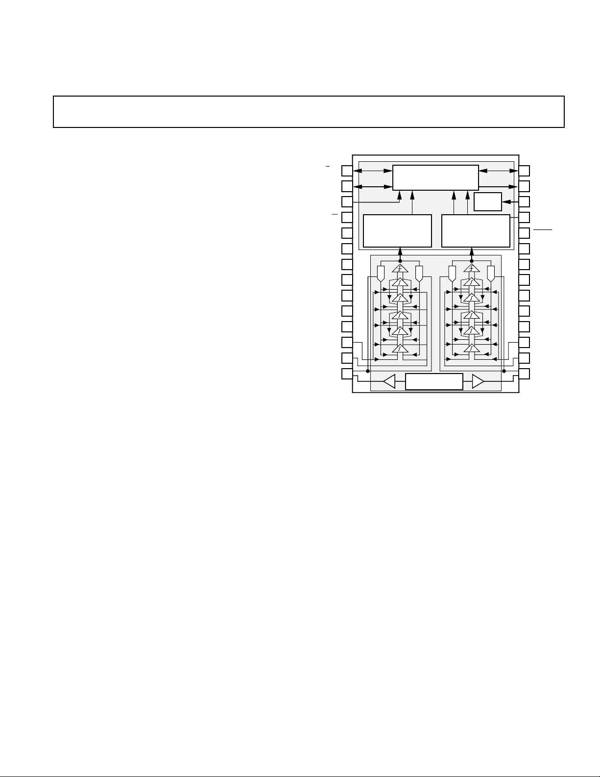
The AD1879 is a two-channel, 18-bit oversampling ADC based
on ∑∆ technology and intended primarily for digital audio applications. The AD1878 is identical to the 18-bit AD1879 except
that it outputs 16-bit data words. Statements in this data sheet
should be read as applying to both parts unless otherwise noted.
Each input channel of these ADCs is fully differential. Each
data conversion channel consists of a fifth order one-bit noise
shaping modulator and a digital decimation filter. An on-chip
voltage reference provides a voltage source to both channels stable over temperature and time. Digital output data from both
channels is time-multiplexed to a single, flexible serial interface.
The AD1878/AD1879 accepts a 256 × F
Input signals are sampled at 64 × F
input master clock.
S
on switched-capacitors,
S
eliminating external sample-and-hold amplifiers and minimizing
the requirements for antialias filtering at the input. With simplified antialiasing, linear phase can be preserved across the passband.
The AD1878/AD1879’s proprietary fifth-order differential
switched-capacitor modulator architecture shapes the one-bit
comparator’s quantization noise out of the audio passband. The
high order of the modulator randomizes the modulator output,
reducing idle tones in the AD1878/AD1879 to very low levels.
The AD1878/AD1879’s differential architecture provides increased dynamic range and excellent common-mode rejection
characteristics. Because its modulator is single-bit, AD1878/
AD1879 is inherently monotonic and has no mechanism for
producing differential linearity errors.
The digital decimation filters are single-stage, 4095-tap finite
impulse response filters for filtering the modulator’s high frequency quantization noise and reducing the 64 × F
output data rate to a F
*
Protected by U.S. Patent Numbers 5055843, 5126653, and others pending.
REV. 0
Information furnished by Analog Devices is believed to be accurate and
reliable. However, no responsibility is assumed by Analog Devices for its
use, nor for any infringements of patents or other rights of third parties
which may result from its use. No license is granted by implication or
otherwise under any patent or patent rights of Analog Devices.
word rate. They provide linear
S
single-bit
S
phase and a narrow transition band that permits the digitization
of 20 kHz signals while preventing aliasing into the passband
even when using a 44.1 kHz sampling frequency. Passband
ripple is less the 0.001 dB, and stopband attenuation exceeds
115 dB.
The flexible serial output port produces data in twos-complement,
MSB-first format. Input and output signals are to TTL and
CMOS-compatible logic levels. The port is configured by pin
selections. The AD1878/AD1879 can operate in either master
or slave mode. Each 16-/18-bit output word of a stereo pair can
be formatted within a 32-bit field as either right-justified, I
compatible, or at user-selected positions. The output can also be
truncated to 16-bits by formatting into a 16-bit field.
The AD1878/AD1879 consists of two integrated circuits in a
single ceramic 28-pin DIP package. The modulators and reference are fabricated in a BiCMOS process; the decimator and
output port, in a 1.0 µm CMOS process. Separating these func-
tions reduces digital crosstalk to the analog circuitry. Analog and
digital supply connections are separated to further isolate the
analog circuitry from the digital supplies.
The AD1878/AD1879 operates from ± 5 V power supplies over
the temperature range of –25°C to +70°C.
One Technology Way, P.O. Box 9106, Norwood, MA 02062-9106, U.S.A.
Tel: 617/329-4700 Fax: 617/326-8703
FUNCTIONAL BLOCK DIAGRAM
2
S-
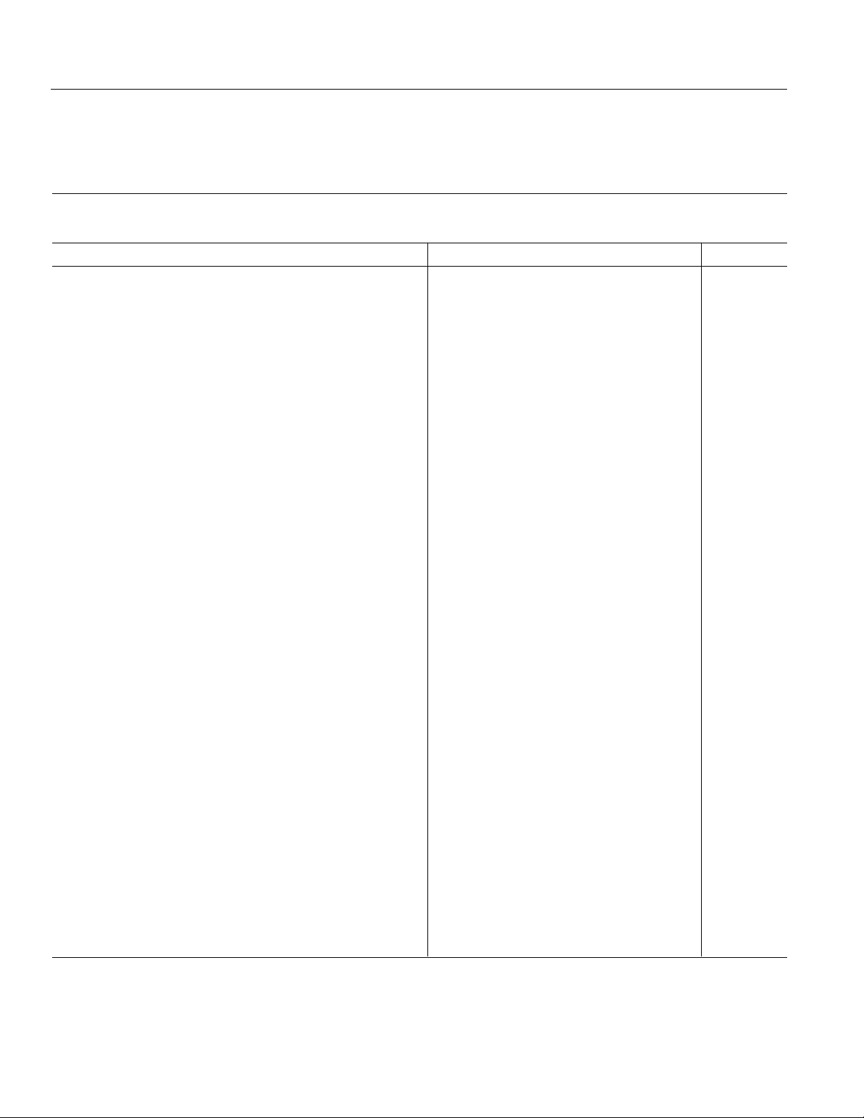
AD1878/AD1879–SPECIFICA TIONS
TEST CONDITIONS UNLESS OTHERWISE NOTED
Supply Voltages ±5V
Ambient Temperature 25 °C
Input Clock (F
Input Signal 974 Hz
All minimums and maximums tested except as noted.
ANALOG PERFORMANCE
AD1879 Resolution 18 Bits
AD1878 Resolution 16 Bits
Clock Input Frequency Range
CLOCK Input (F
Modulator Sample Rate (F
Output Word Rate (F
AD1879 Dynamic Range (0 kHz to 20 kHz, –60 dB input)
Stereo Mode (No A-Weight Filter) 100 103 dB
Mono Mode
Stereo Mode (with A-Weight Filter) 105 dB
AD1879 Trimmed
Full Scale 93 98 dB
–20 dB 83 dB
AD1879 Untrimmed
Full Scale 91 96 dB
–20 dB 83 dB
AD1879 Trimmed
Full Scale 98 dB
–20 dB 100 dB
AD1878 Dynamic Range (0 kHz to 20 kHz, –60 dB 1.0936 kHz
Input Dithered with a –10 dB 21.873 kHz Sine Wave)
Stereo Mode (No A-Weight Filter) 95 97 dB
AD1878 Trimmed
Full Scale 93 95 dB
–20 dB 77 dB
AD1878 Untrimmed
Full Scale 91 94 dB
–20 dB 77 dB
AD1878 Trimmed
Full Scale 98 dB
–20 dB 100 dB
Analog Inputs
Differential Input Range
Input Impedance at Each Input Pin 7.0 kΩ
DC Accuracy
Gain Error ±1 ±5%
Interchannel Gain Mismatch 0.05 0.15 dB
Gain Drift 150 ppm/°C
AD1879 Midscale Offset Error ±200 ±750 18-Bit LSBs
AD1878 Midscale Offset Error ±50 ±200 16-Bit LSBs
Midscale Drift 13 ppm/°C
Voltage Reference 2.4 2.86 3.2 V
Crosstalk (EIAJ Method) 100 105 dB
Interchannel Phase Deviation ±0.001 Degrees
NOTES
1
Both channels connected together for mono operations as described below in “How to Extend SNR.”
2
Differential gain imbalance manually trimmed to eliminate second harmonic. See “Applications Issues” below.
3
Test performed without part-to-part trimming.
4
The differential input range is twice the range seen at each input pin. The input range corresponds to the full-scale digital output range.
Specifications subject to change without notice.
) 12.288 MHz
CLOCK
–0.5 dB Full Scale
Min Typ Max Units
) 0.01 12.288 14.286 MHz
CLOCK
= F
S
1
(No A-Weight Filter) 106 dB
2
Signal to (Noise + Distortion)
3
Signal to (Noise + Distortion)
2
Signal to Total Harmonic Distortion
2
Signal to (Noise + Distortion)
3
Signal to (Noise + Distortion)
2
Signal to Total Harmonic Distortion
4
/4) 0.0025 3.072 3.5715 MHz
CLOCK
/256) 0.039 48 55.8 kHz
CLOCK
±5.985 ±6.3 ±6.615 V
–2–
REV. 0
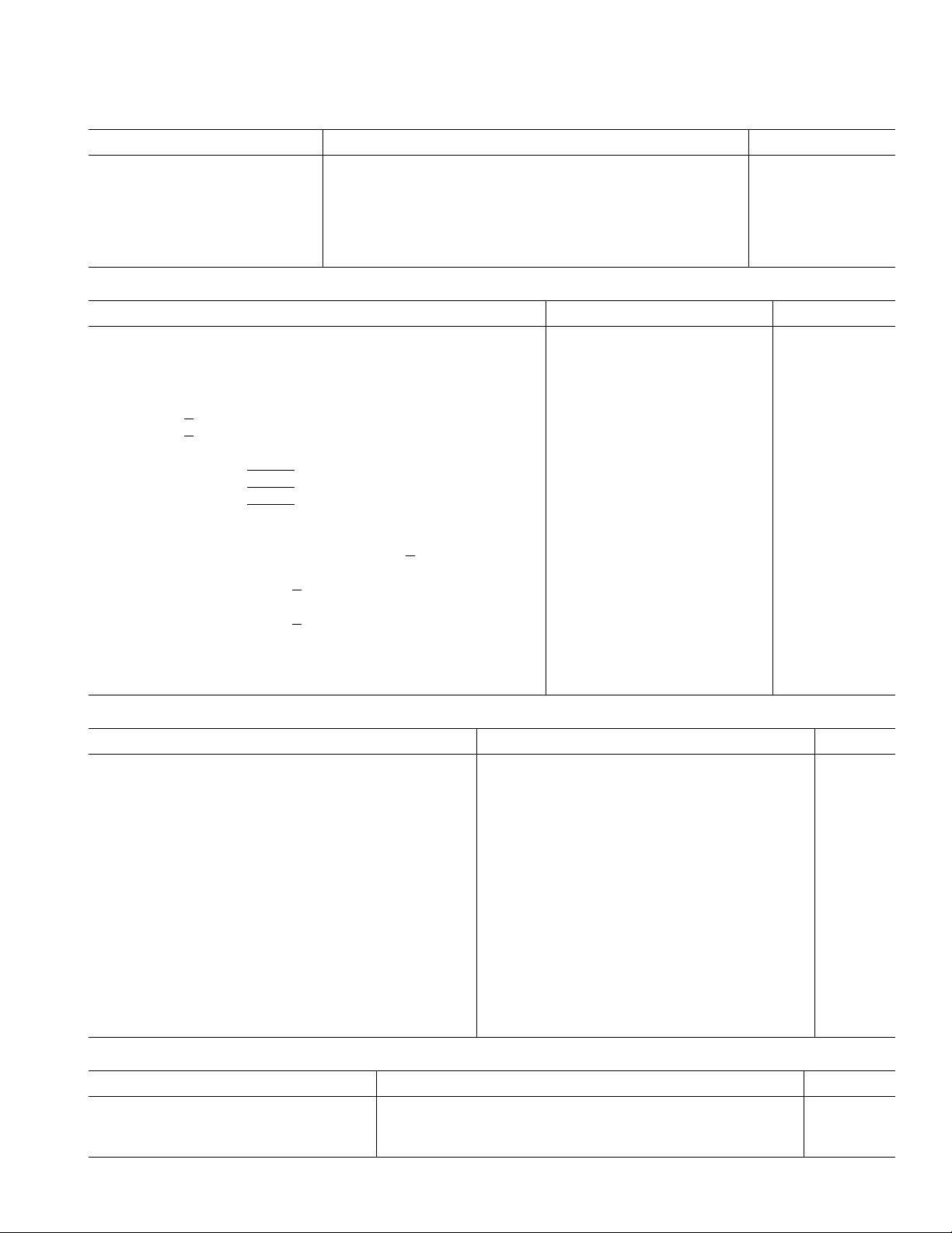
DIGITAL INPUTS
AD1878/AD1879
Min Max Units
V
IH
V
IL
I
@ VIH = 5 V 10 µA
IH
I
@ VIL = 0 V 10 µA
IL
V
@ IOH = 360 µA 4.0 V
OH
0.8 V
V
VOL @ IOL = 1.6 mA 0.5 V
DIGITAL TIMING
Min Typ Max Units
CLOCK
Period (T
CLOCK
= 1/F
) 0.07 100 µs
CLOCK
LO Pulse Width 35 ns
HI Pulse Width 35 ns
BCK Pulse Width 2 CLOCK Periods
64-Bit Frame L
32-Bit Frame L
RCK Pulse Width 32 BCK Periods
RCK Pulse Width 16 BCK Periods
WCK Pulse Width 1 BCK Periods
t
RSET
t
RHLD
t
RSLS
t
WSET
t
WHLD
t
DLYCK
RESET Setup to CLOCK Rising 5 ns
RESET Hold from CLOCK Rising 20 ns
RESET Pulse Width 4 10 µs CLOCK Periods
WCK to CLOCK Rising 5 ns
WCK Hold from CLOCK Rising 20 ns
CLOCK to BCK/WCK/LRCK Delay 65 ns
(Master Mode)
t
SET
BCK/LRCK to CLOCK Falling 5 ns
(Slave Mode)
t
HLD
BCK/LRCK Hold from CLOCK Falling 20 ns
(Slave Mode)
t
DLYD, MSB
t
DLYD
CLOCK Falling to MSB DATA Delay 65 ns
CLOCK Rising to DATA Delay, Except MSB 70 ns
POWER
Min Typ Max Units
Supplies
Voltage, DV
Voltage, AV
Current, AV
Current, AV
Current, AV
Current, DV
/AVDD1/AVDD2 4.75 5 5.25 V
DD
1/AVSS2 –5.25 –5 –4.75 V
SS
1/AVSS17392mA
DD
1/AVSS1—Power Down 13 23 mA
DD
2/AVSS2 8 10 mA
DD
DD
64 70 mA
Dissipation
Operation 1,130 1,370 mW
Operation—Analog Supplies 810 1,020 mW
Operation—Digital Supplies 320 350 mW
Power Down (All Supplies) 530 680 mW
Power Supply Rejection
1 kHz 300 mV p-p Signal at Analog Supply Pins 102 dBFS
Passband—Any 300 mV p-p Signal 92 dBFS
Stopband—Any 300 mV p-p Signal 105 dBFS
TEMPERATURE RANGE
Min Typ Max Units
Specifications Guaranteed +25 °C
Functionality Guaranteed –25 +70 °C
Storage –60 +100 °C
REV. 0
–3–
AD1878/AD1879
WARNING!
ESD SENSITIVE DEVICE
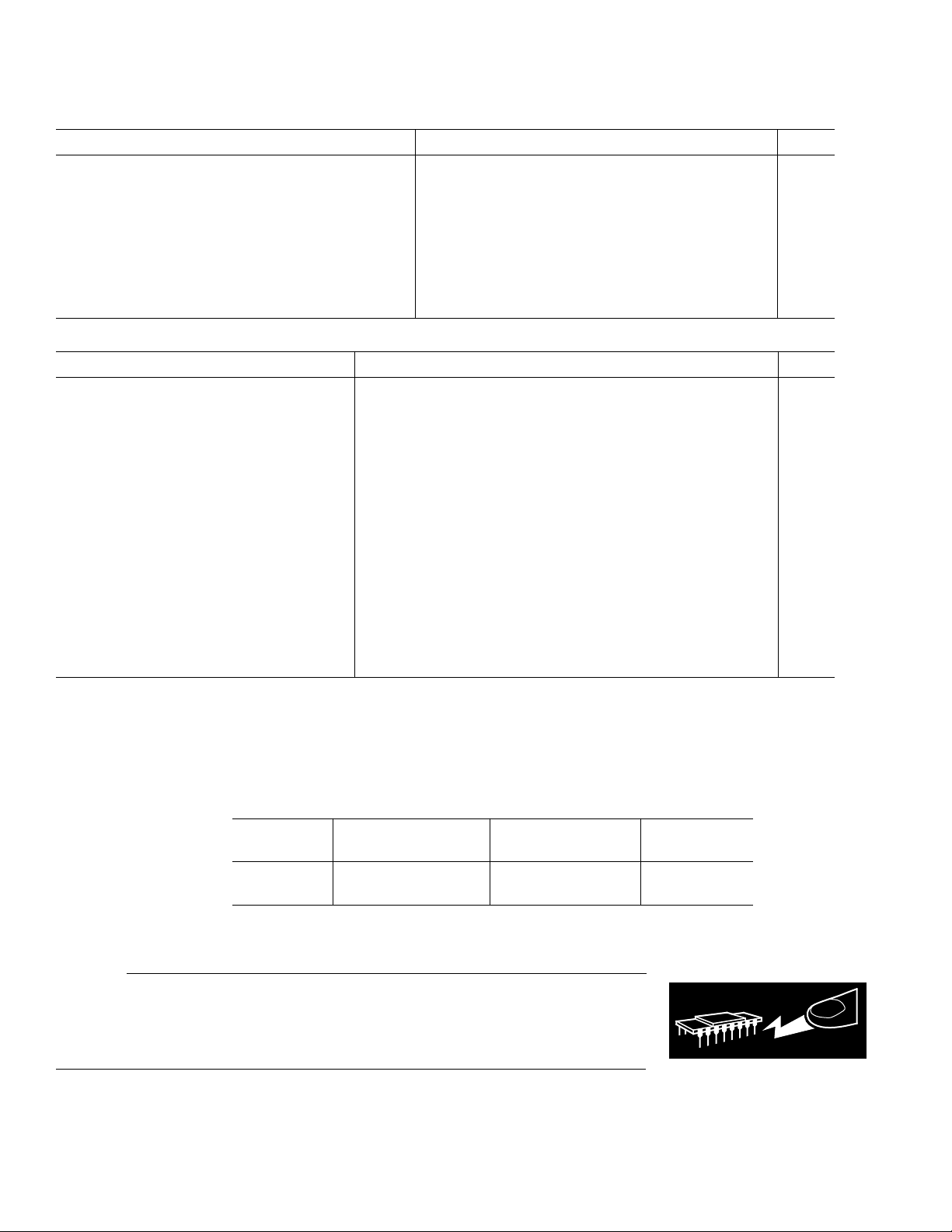
ABSOLUTE MAXIMUM RATINGS
Min Typ Max Units
DVDD to DGND and AVDD1/AVDD2 to AGND 0 6 V
AV
1/AVSS2 to AGND –6 0 V
SS
AV
2 to AVSS1 –0.3 V
SS
Digital Inputs to DGND –0.3 DV
Analog Inputs AV
1 – 0.3 AVDD1 + 0.3 V
SS
AGND to DGND –0.3 0.3 V
Reference Voltage Indefinite Short Circuit to Ground
Soldering +300 °C
DIGITAL FILTER CHARACTERISTICS
Min Typ Max Units
Decimation Factor 64
Passband Ripple 0.001 dB
Stopband
48 kHz F
1
Attenuation 115 dB
(12.288 MHz CLOCK)
S
Passband 0 21.7 kHz
Stopband 26.2 3,045 kHz
44.1 kHz F
(11.2896 MHz CLOCK)
S
Passband 0 20.0 kHz
Stopband 24.1 2,798 kHz
32 kHz F
(8.192 MHz CLOCK)
S
Passband 0 14.5 kHz
Stopband 17.5 2,030 kHz
Other F
S
Passband 0 0.4535 F
Stopband 0.5458 63.4542 F
Group Delay ([4096/2]/[64 × FS]) 32/F
S
Group Delay Variation 0 µs
NOTE
1
Stopband repeats itself at multiples of 64 × FS, where FS is the output word rate. Thus the digital filter will attenuate to 115 dB across the frequency spectrum
except for a range ±0.5458 × FS wide at multiples of 64 × FS.
Specifications subject to change without notice.
+ 0.3 V
DD
10 sec
S
S
ORDERING GUIDE
Package Package
Model Temperature Description Option
AD1878JD –25°C to +70°C Ceramic DIP D-28
AD1879JD –25°C to +70°C Ceramic DIP D-28
CAUTION
ESD (electrostatic discharge) sensitive device. Electrostatic charges as high as 4000 V readily
accumulate on the human body and test equipment and can discharge without detection.
Although the AD1878/AD1879 features proprietary ESD protection circuitry, permanent damage may occur on devices subjected to high energy electrostatic discharges. Therefore, proper
ESD precautions are recommended to avoid performance degradation or loss of functionality.
REV. 0–4–
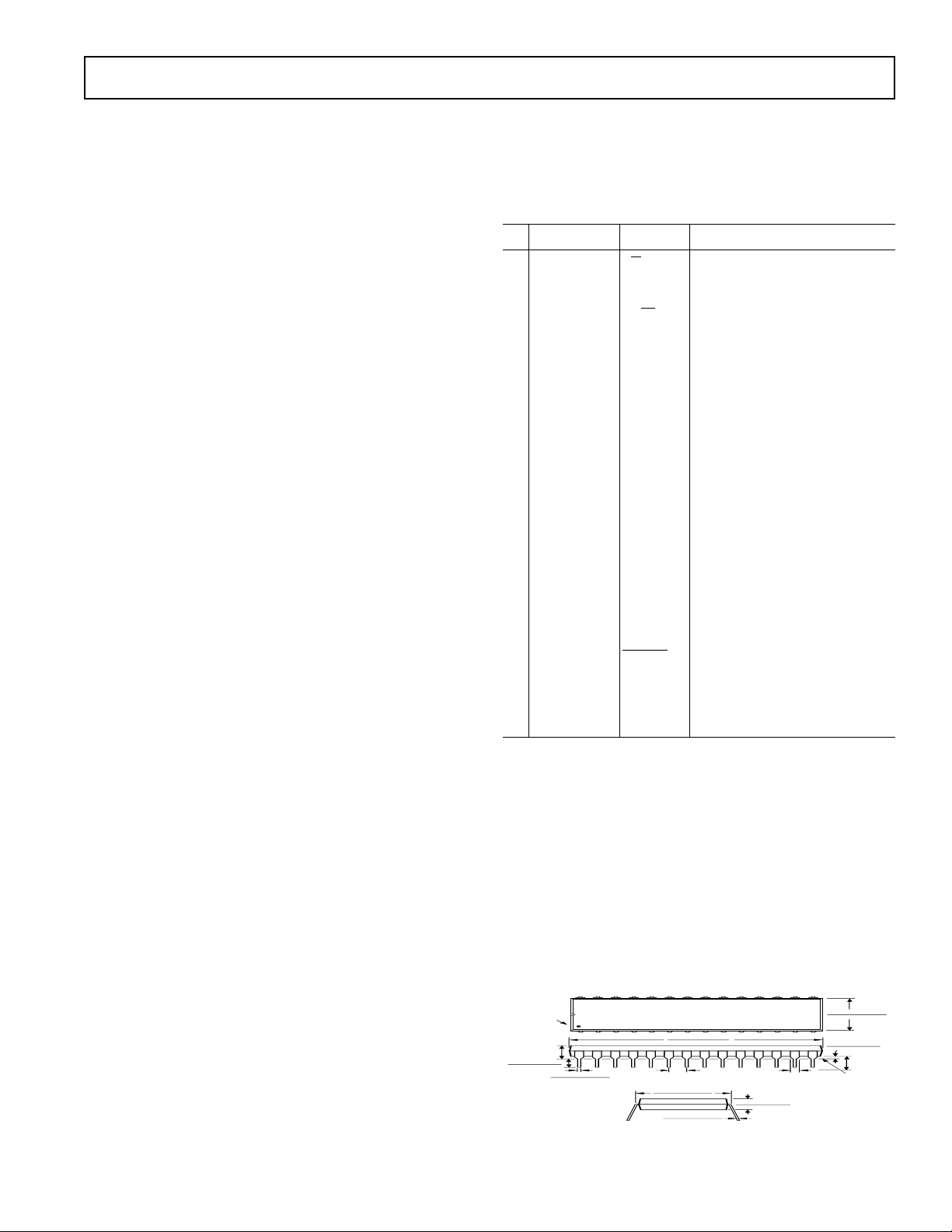
AD1878/AD1879
PIN 1
0.580 (14.73)
0.485 (12.32)
1
14
15
2
8
0.625 (15.87)
0.600 (15.24)
0.015 (0.381)
0.008 (0.204)
0.195 (4.95)
0.125 (3.18)
0.250
(6.35)
MAX
0.022 (0.558)
0.014 (0.356)
0.100
(2.54)
BSC
0.200 (5.05)
0.125 (3.18)
0.070 (1.77)
MAX
0.060 (1.52)
0.015 (0.38)
0.150
(3.81)
MIN
SEATING
PLANE
1.565 (39.70)
1.380 (35.10)
DEFINITIONS
Dynamic Range
The ratio of a full-scale output signal to the integrated output
noise in the passband (0 kHz to 20 kHz), expressed in decibels
Group Delay Variation
The difference in group delays at different input frequencies.
Specified as the difference between largest and the smallest
group delays in the passband, expressed in microseconds (µs).
(dB). Dynamic range is measured with a –60 dB input signal
and is equal to (S/[THD+N]) + 60 dB.
Signal to (Noise + Distortion)
The ratio of the root-mean-square (rms) value of the fundamental input signal to the rms sum of all spectral components in the
passband, expressed in decibels (dB).
Signal to Total Harmonic Distortion (THD)
The ratio of the rms sum of all harmonically related spectral
components in the passband to the fundamental input signal,
expressed either as a percentage (%) or in decibels (dB).
Passband
The region of the frequency spectrum unaffected by the attenuation of the digital decimator’s filter.
Passband Ripple
The peak-to-peak variation in amplitude response from equal
amplitude input signal frequencies within the passband, expressed in decibels.
Stopband
The region of the frequency spectrum attenuated by the digital decimator’s filter to the degree specified by “stopband
attenuation.”
Gain Error
With a near full-scale input, the ratio of actual output to expected output, expressed as a percentage.
Interchannel Gain Mismatch
With near full-scale inputs, the ratio of outputs of the two stereo
channels, expressed in decibels.
Gain Drift
Change in response to a near full-scale input with a change in
temperature, expressed as parts-per-million (ppm) per °C.
Pin Input/Output Pin Name Description
11 I/O L
12 I/O BCK Bit Clock
13 I S0 Mode Select 0
14 I 64/
15I DV
16 I DGND Digital Ground
17 N/C No Connection; Do Not Connect
18I AV
19I AV
10 I AGND Analog Ground
11 I APD Analog Power Down
12 I VINR– Right Inverting Input
13 I VINR+ Right Noninverting Input
14 I/O REFR Right Reference Capacitor
15 I/O REFL Left Reference Capacitor
16 I VINL+ Left Noninverting Input
17 I VINL– Left Inverting Input
18 I AGND Analog Ground
19 I AV
20 I AV
21 I AV
22 I DV
23 I DGND Digital Ground
24 I
25 I S1 Mode Select 1
26 I CLOCK Master Clock Input
27 O DATA Serial Data Output
28 I/O WCK Word Clock
AD1878/AD1879 PIN LIST
RCK Left/Right Clock
32 Bit Rate Select
DD
SS
SS
DD
DD
SS
DD
+5 V Digital Supply
1 –5 V Analog Supply
2 –5 V Analog Logic Supply
1 +5 V Analog Supply
2 +5 V Analog Logic Supply
1 –5 V Analog Supply
+5 V Digital Supply
RESET Reset
Midscale Offset Error
Output response to a midscale input (i.e., zero volts dc), expressed in least-significant bits (LSBs).
Midscale Drift
Change in midscale offset error with a change in temperature,
expressed as parts-per-million (ppm) of full scale per °C.
Crosstalk
Ratio of response on one channel with a grounded input to a
full-scale 1 kHz sine-wave input on the other channel, expressed
in decibels.
Interchannel Phase Deviation
Difference in input sampling times between stereo channels, expressed as a phase difference in degrees between 1 kHz inputs.
THEORY OF OPERATION
Modulator Noise-Shaping
∑∆
The stereo, differential analog modulators of the AD1878/
AD1879 employ a proprietary feedforward and feedback archi-
tecture that passes input signals in the audio band with a unity
transfer function yet simultaneously shape the quantization
noise generated by the one-bit comparator out of the audio
band. See Figure 1. Without the ∑∆ architecture, this quantiza-
tion noise would be spread uniformly from dc to one-half the
oversampling frequency, 64 × F
. (Regardless of architecture,
S
64 times oversampling by itself significantly reduces the quanti-
zation noise in the audio band if the input is properly dithered.
However, the noise reduction is only [log
64] × 3 dB = 18 dB.)
2
Power Supply Rejection
With analog inputs grounded, energy at the output when a
300 mV p-p signal is applied to power supply pins, expressed in
decibels of full scale.
Group Delay
Intuitively, the time interval required for an input pulse to appear at the converter’s output, expressed in milliseconds (ms).
More precisely, the derivative of radian phase with respect to
radian frequency at a given frequency.
REV. 0
Figure 1. AD1878/AD1879 Modulator Noise-Shaper (One
Channel)
–5–
 Loading...