Single-Supply
a
FEATURES
Single 5 V Power Supply
Single-Ended Dual-Channel Analog Inputs
92 dB (Typ) Dynamic Range
90 dB (Typ) S/(THD + N)
0.006 dB Decimator Passband Ripple
Fourth-Order, 64ⴛ Oversampling ⌺-⌬ Modulator
Three-Stage, Linear-Phase Decimator
256 ⴛ f
Less than 100 W (Typ) Power-Down Mode
Input Overrange Indication
On-Chip Voltage Reference
Flexible Serial Output Interface
28-Lead SOIC Package
APPLICATIONS
Consumer Digital Audio Receivers
Digital Audio Recorders, Including Portables
Multimedia and Consumer Electronics Equipment
Sampling Music Synthesizers
PRODUCT OVERVIEW
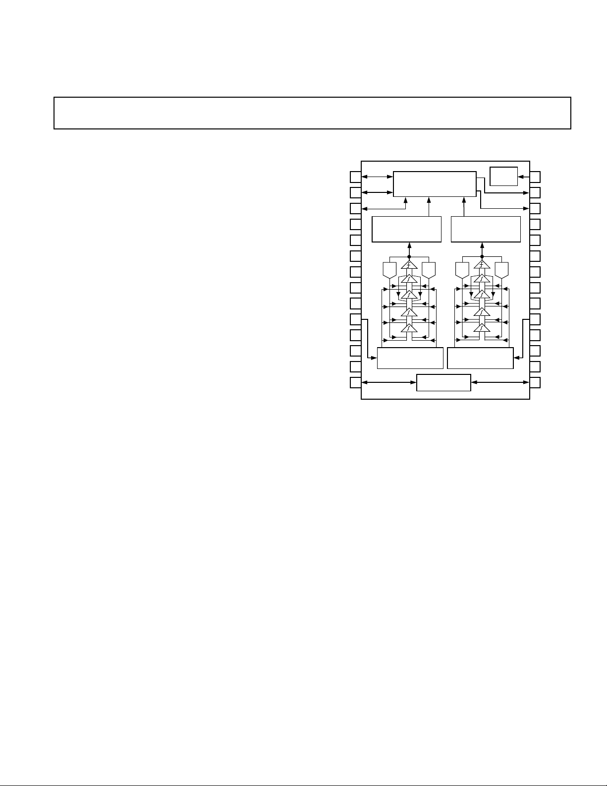
The AD1870 is a stereo, 16-bit oversampling ADC based on
sigma-delta (∑-∆) technology intended primarily for digital
audio bandwidth applications requiring a single 5 V power supply.
Each single-ended channel consists of a fourth-order one-bit
noise shaping modulator and a digital decimation filter. An onchip voltage reference, stable over temperature and time, defines
the full-scale range for both channels. Digital output data from
both channels are time-multiplexed to a single, flexible serial
interface. The AD1870 accepts a 256 × f
clock (f
port “master” and “slave” modes. In slave mode, all clocks must
be externally derived from a common source.
Input signals are sampled at 64 × f
switched-capacitors, eliminating external sample-and-hold amplifiers and minimizing the requirements for antialias filtering at the
input. With simplified antialiasing, linear phase can be preserved
across the passband. The on-chip single-ended to differential signal
converters save the board designer from having to provide them
externally. The AD1870’s internal differential architecture provides
increased dynamic range and excellent power supply rejection
characteristics. The AD1870’s proprietary fourth-order differential switched-capacitor ∑-∆ modulator architecture shapes the
*Protected by U.S. Patent Numbers 5055843, 5126653; others pend ing.
or 384 ⴛ fS Input Clock
S
CD-R, DCC, MD, and DAT
or a 384 × fS input
is the sampling frequency) and operates in both serial
S
S
onto internally buffered
S
16-Bit ⌺-⌬ Stereo ADC
AD1870*
FUNCTIONAL BLOCK DIAGRAM
LRCK
WCLK
BCLK
DV
DD
DGND1
RDEDGE
S/M
384/256
AV
VINL
CAPL1
CAPL2
AGNDL
V
REF
1
2
3
THREE-STAGE FIR
4
1
5
6
7
8
9
DD
10
11
12
DIFFERENTIAL INPUT
13
14
L
SERIAL OUTPUT
DECIMATION
FILTER
DAC
SINGLE-TO-
CONVERTER
INTERFACE
THREE-STAGE FIR
DAC DAC DAC
SINGLE-TO-
DIFFERENTIAL INPUT
CONVERTER
VOLTAGE
REFERENCE
one-bit comparator’s quantization noise out of the audio passband. The high order of the modulator randomizes the modulator
output, reducing idle tones in the AD1870 to very low levels.
Because its modulator is single-bit, the AD1870 is inherently
monotonic and has no mechanism for producing differential
linearity errors.
The input section of the AD1870 uses autocalibration to correct
any dc offset voltage present in the circuit, provided that the inputs
are ac-coupled. The single-ended dc input voltage can swing
between 0.7 V and 3.8 V typically. The AD1870 antialias input
circuit requires four external 470 pF NPO ceramic chip filter
capacitors, two for each channel. No active electronics are needed.
Decoupling capacitors for the supply and reference pins are
also required.
The dual digital decimation filters are triple-stage, finite impulse
response filters for effectively removing the modulator’s high
frequency quantization noise and reducing the 64 × f
output data rate to an f
word rate. They provide linear phase
S
and a narrow transition band that properly digitizes 20 kHz signals
at a 44.1 kHz sampling frequency. Passband ripple is less than
0.006 dB, and stop band attenuation exceeds 90 dB.
CLOCK
DIVIDER
DECIMATION
FILTER
AD1870
CLKIN
28
27
TAG
26
SOUT
DV
2
25
DD
24
DGND2
23
RESET
22
MSBDLY
21
RLJUST
20
AGND
R
V
19
IN
CAPR1
18
17
CAPR2
AGNDR
16
R
V
15
REF
single-bit
S
(Continued on Page 7)
REV. 0
Information furnished by Analog Devices is believed to be accurate and
reliable. However, no responsibility is assumed by Analog Devices for its
use, nor for any infringements of patents or other rights of third parties that
may result from its use. No license is granted by implication or otherwise
under any patent or patent rights of Analog Devices.
One Technology Way, P.O. Box 9106, Norwood, MA 02062-9106, U.S.A.
Tel: 781/329-4700 www.analog.com
Fax: 781/326-8703 © Analog Devices, Inc., 2001

AD1870–SPECIFICATIONS
TEST CONDITIONS UNLESS OTHERWISE NOTED
Supply Voltages 5.0 V
Ambient Temperature 25 °C
Input Clock (f
Input Signal 991.768 Hz
Measurement Bandwidth 23.2 Hz to 19.998 kHz
Load Capacitance on Digital Outputs 50 pF
Input Voltage HI (V
Input Voltage LO (V
Master Mode, Data I
Device Under Test (DUT) bypassed and decoupled as shown in Figure 3.
DUT is antialiased and ac-coupled as shown in Figure 2. DUT is calibrated.
Values in bold typeface are tested, all others are guaranteed but not tested.
ANALOG PERFORMANCE
Resolution 16 Bits
Dynamic Range (20 Hz to 20 kHz, –60 dB Input)
Without A-Weight Filter 89 93 dB
With A-Weight Filter 92 96 dB
Signal to (THD + Noise) 86.5 90.5 dB
Signal to THD 94 dB
Analog Inputs
Single-Ended Input Range (± Full Scale)* V
Input Impedance at Each Input Pin 32 kΩ
V
REF
DC Accuracy
Gain Error ±0.5 ⴞ2.5 %
Interchannel Gain Mismatch 0.05 dB
Gain Drift 115 ppm/°C
Midscale Offset Error (After Calibration) ±3 ⴞ20 LSBs
Midscale Drift –0.2 LSB/°C
Crosstalk (EIAJ Method) –110 –100 dB
*VIN p-p = V
REF
) [256 × fS] 12.288 MHz
CLKIN
–0.5 dB Full Scale
) 2.4 V
IH
) 0.8 V
IL
2
S-Justified (Refer to Figure 14).
× 1.326.
Min Typ Max Unit
± 1.49 V
REF
2.05 2.25 2.55 V
Minimum Input V
Maximum Input V
V
–
=
REF
=+
V
REF
×
..1 326
2
×
1 326
2
–2–
REV. 0
REF
REF

AD1870
DIGITAL I/O
Min Typ Max Unit
Input Voltage HI (V
Input Voltage LO (V
Input Leakage (I
Input Leakage (I
Output Voltage HI (V
Output Voltage LO (V
Input Capacitance 15 pF
DIGITAL TIMING (Guaranteed over –40°C to +85°C, DVDD = AVDD = 5 V ± 5%. Refer to Figures 17–19.)
t
CLKIN
f
CLKIN
t
CPWL
t
CPWH
t
RPWL
t
BPWL
t
BPWH
t
DLYCKB
t
DLYBLR
t
DLYBWR
t
DLYBWF
t
DLYDT
t
SETLRBS
t
DLYLRDT
t
SETWBS
t
DLYBDT
) 2.4 V
IH
) 0.8 V
IL
@ VIH = 5 V) 10 µA
IH
@ VIL = 0 V) 10 µA
IL
@ IOH = –2 mA) 2.4 V
OH
@ IOL = 2 mA) 0.4 V
OL
Min Typ Max Unit
CLKIN Period 48 81 780 ns
CLKIN Frequency (1/t
) 1.28 12.288 20.48 MHz
CLKIN
CLKIN LO Pulsewidth 15 ns
CLKIN HI Pulsewidth 15 ns
RESET LO Pulsewidth 50 ns
BCLK LO Pulsewidth 15 ns
BCLK HI Pulsewidth 15 ns
CLKIN Rise to BCLK Xmit (Master Mode) 15 ns
BCLK Xmit to LRCK Transition (Master Mode) 15 ns
BCLK Xmit to WCLK Rise 10 ns
BCLK Xmit to WCLK Fall 10 ns
BCLK Xmit to DATA/TAG Valid (Master Mode) 10 ns
LRCK Setup to BCLK Sample (Slave Mode) 10 ns
LRCK Transition to DATA/TAG Valid (Slave Mode)
No MSB Delay Mode (for MSB Only) 40 ns
WCLK Setup to BCLK Sample (Slave Mode)
Data Position Controlled by WCLK Input Mode 10 ns
BCLK Xmit to DATA/TAG Valid (Slave Mode)
All Bits Except MSB in No MSB Delay Mode
All Bits in MSB Delay Mode 40 ns
POWER
Min Typ Max Unit
Supplies
Voltage, Analog and Digital 4.75 5 5.25 V
Analog Current 43 52 mA
Analog Current—Power Down (CLKIN Running) 25 µA
Digital Current 9.3 12 mA
Digital Current—Power Down (CLKIN Running) 50 µA
Dissipation
Operation—Both Supplies 263 315 mW
Operation—Analog Supply 216 260 mW
Operation—Digital Supply 47 55 mW
Power Down—Both Supplies (CLKIN Running) 375 µW
Power Down—Both Supplies (CLKIN Not Running) 375 µW
Power Supply Rejection (See TPC 5)
1 kHz 300 mV p-p Signal at Analog Supply Pins 90 dB
20 kHz 300 mV p-p Signal at Analog Supply Pins 68 dB
Stop Band (>0.55 × fS)—any 300 mV p-p Signal 110 dB
REV. 0
–3–

WARNING!
ESD SENSITIVE DEVICE
AD1870–SPECIFICATIONS
TEMPERATURE RANGE
Min Typ Max Unit
Specifications Guaranteed 25 °C
Functionality Guaranteed –40 +85 °C
Storage –60 +100 °C
DIGITAL FILTER CHARACTERISTICS
Min Typ Max Unit
Decimation Factor 64
Passband Ripple 0.006 dB
Stop Band
48 kHz f
Passband 0 21.6 kHz
Stop Band 26.4 kHz
44.1 kHz f
Passband 0 20 kHz
Stop Band 24.25 kHz
32 kHz f
Passband 0 14.4 kHz
Stop Band 17.6 kHz
Other f
Passband 0 0.45 f
Stop Band 0.55 f
Group Delay 36/f
Group Delay Variation 0 µs
NOTES
1
Stop band repeats itself at multiples of 64 × fS, where fS is the output word rate. Thus the digital filter will attenuate to 0 dB across the frequency spectrum except
for a range ± 0.55 × fS wide at multiples of 64 × fS.
Specifications subject to change without notice.
1
Attenuation 90 dB
(at Recommended Crystal Frequencies)
S
(at Recommended Crystal Frequencies)
S
(at Recommended Crystal Frequencies)
S
S
S
S
S
s
ABSOLUTE MAXIMUM RATINGS
Min Typ Max Unit
1 to DGND1 and DVDD2 to DGND2 0 6 V
DV
DD
to AGND/AGNDL/AGNDR 0 6 V
AV
DD
Digital Inputs DGND – 0.3 DV
Analog Inputs AGND – 0.3 AV
+ 0.3 V
DD
+ 0.3 V
DD
AGND to DGND –0.3 +0.3 V
Reference Voltage Indefinite Short Circuit to Ground
Soldering (10 sec) 300 °C
ORDERING GUIDE
Package Package
Model Temperature Description Option
AD1870JR –40°C to +85°C SOIC R-28
CAUTION
ESD (electrostatic discharge) sensitive device. Electrostatic charges as high as 4000 V readily
accumulate on the human body and test equipment and can discharge without detection. Although
the AD1870 features proprietary ESD protection circuitry, permanent damage may occur on
devices subjected to high-energy electrostatic discharges. Therefore, proper ESD precautions are
recommended to avoid performance degradation or loss of functionality.
–4–
REV. 0

AD1870
PIN FUNCTION DESCRIPTIONS
Input/ Pin
Pin Output Name Description
1 I/O LRCK Left/Right Clock
2 I/O WCLK Word Clock
3 I/O BCLK Bit Clock
4I DV
1 5 V Digital Supply
DD
5 I DGND1 Digital Ground
6 I RDEDGE Read Edge Polarity Select
7I S/M Slave/Master Select
8 I 384/256 Clock Mode
9I AV
10 I V
DD
L Left Channel Input
IN
5 V Analog Supply
11 O CAPL1 Left External Filter Capacitor 1
12 O CAPL2 Left External Filter Capacitor 2
13 I AGNDL Left Analog Ground
14 O V
15 O V
L Left Reference Voltage Output
REF
R Right Reference Voltage Output
REF
16 I AGNDR Right Analog Ground
17 O CAPR2 Right External Filter Capacitor 2
18 O CAPR1 Ri
19 I V
R Right Channel Input
IN
ght External Filter
Capacitor 1
20 I AGND Analog Ground
21 I RLJUST Right/Left Justify
22 I MSBDLY Delay MSB One BCLK Period
23 I RESET Reset
24 I DGND2 Digital Ground
25 I DV
2 5 V Digital Supply
DD
26 O SOUT Serial Data Output
27 O TAG Serial Overrange Output
28 I CLKIN Master Clock
DEFINITIONS
Dynamic Range
The ratio of a full-scale output signal to the integrated output
noise in the passband (20 Hz to 20 kHz), expressed in decibels
(dB). Dynamic range is measured with a –60 dB input signal
and is equal to (S/(THD + N)) 60 dB. Note that spurious harmonics are below the noise with a –60 dB input, so the noise
level establishes the dynamic range. The dynamic range is specified with and without an A-Weight filter applied.
Signal to (Total Harmonic Distortion + Noise)
(S/(THD + N))
The ratio of the root-mean-square (rms) value of the fundamental input signal to the rms sum of all other spectral components
in the passband, expressed in decibels (dB).
Signal to Total Harmonic Distortion (S/THD)
The ratio of the rms value of the fundamental input signal to the
rms sum of all harmonically related spectral components in the
passband, expressed in decibels.
Passband
The region of the frequency spectrum unaffected by the attenuation of the digital decimator’s filter.
Passband Ripple
The peak-to-peak variation in amplitude response from equalamplitude input signal frequencies within the passband,
expressed in decibels.
Stop Band
The region of the frequency spectrum attenuated by the digital decimator’s filter to the degree specified by “stop band
attenuation.”
Gain Error
With a near full-scale input, the ratio of actual output to
expected output, expressed as a percentage.
Interchannel Gain Mismatch
With identical near full-scale inputs, the ratio of outputs of the
two stereo channels, expressed in decibels.
Gain Drift
Change in response to a near full-scale input with a change in
temperature, expressed as parts-per-million (ppm) per °C.
Midscale Offset Error
Output response to a midscale dc input, expressed in leastsignificant bits (LSBs).
Midscale Drift
Change in midscale offset error with a change in temperature,
expressed as parts-per-million (ppm) per °C.
Crosstalk (EIAJ Method)
Ratio of response on one channel with a grounded input to a
full-scale 1 kHz sine-wave input on the other channel, expressed
in decibels.
Power Supply Rejection
With no analog input, signal present at the output when a
300 mV p-p signal is applied to power supply pins, expressed in
decibels of full scale.
Group Delay
Intuitively, the time interval required for an input pulse to
appear at the converter’s output, expressed in milliseconds
(ms). More precisely, the derivative of radian phase with respect
to radian frequency at a given frequency.
Group Delay Variation
The difference in group delays at different input frequencies.
Specified as the difference between largest and the smallest
group delays in the passband, expressed in microseconds (µs).
REV. 0
–5–

AD1870
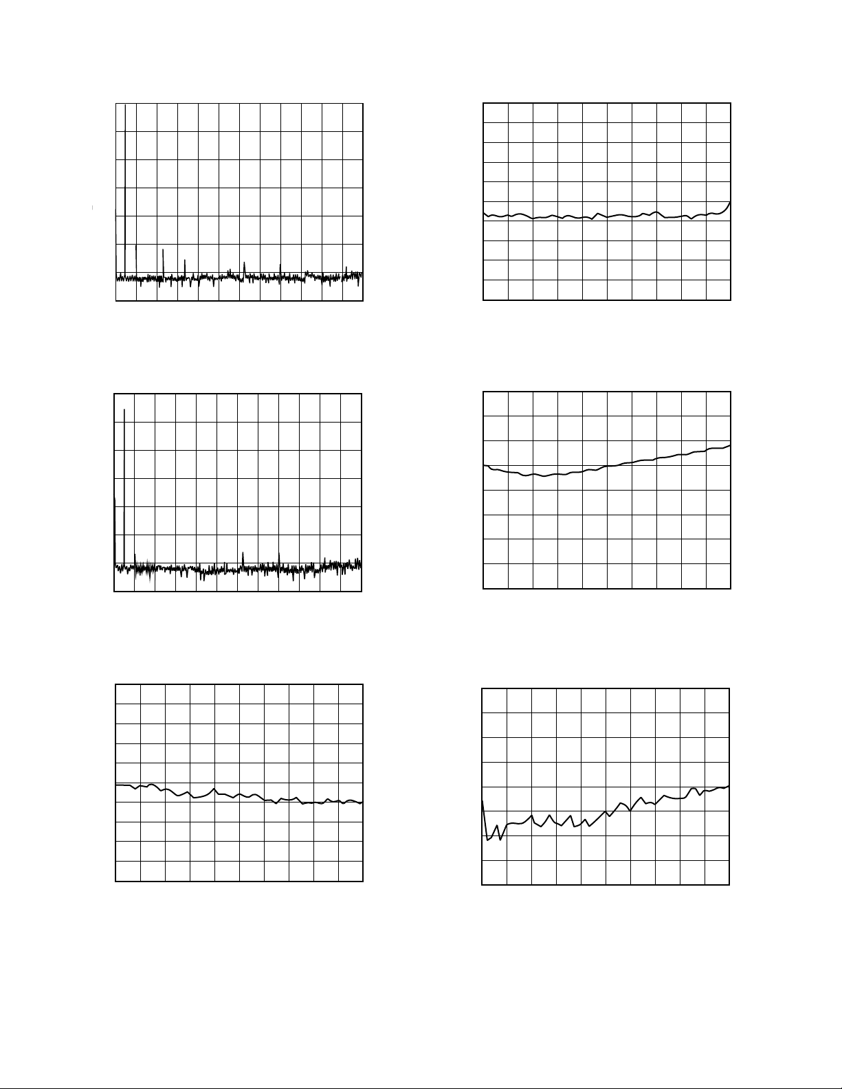
–Typical Performance Characteristics
0
–20
–40
–60
–80
dBFS
–100
–120
–140
2022201816141210864
FREQUENCY – kHz
TPC 1. 1 kHz Tone at –0.5 dBFS (16k-Point FFT)
0
–20
–40
–60
dBFS
–80
–100
–120
–80
–82
–84
–86
–88
–90
dBFS
–92
–94
–96
–98
24
–100
2
0
AMPLITUDE – dBFS
1816141210864
TPC 4. THD + N vs. Amplitude at 1 kHz
–60
–65
–70
–75
–80
dBFS
–85
–90
–95
–140
2
0
FREQUENCY – kHz
TPC 2. 1 kHz Tone at –10 dBFS (16k-Point FFT)
–80
–82
–84
–86
–88
–90
dBFS
–92
–94
–96
–98
–100
2
0
FREQUENCY – kHz
TPC 3. THD + N vs.Frequency at –0.5 dBFS
22201816141210864
24
–100
20
AMPLITUDE – kHz
TPC 5. Power Supply Rejection to 300 mV p-p on AV
–80
–85
–90
–95
–100
dBFS
–105
–110
–115
20
1816141210864
–120
2
0
FREQUENCY – kHz
20
1816141210864
DD
20
1816141210864
TPC 6. Channel Separation vs. Frequency at –0.5 dBFS
–6–
REV. 0
 Loading...