

Page 1

HardCopy II Clock Uncertainty Calculator
User Guide
101 Innovation Drive
San Jose, CA 95134
www.altera.com
Software Version: 7.1
Document Version: 1.0
Document Date: August 2007
Page 2

Copyright © 2007 Altera Corporation. All rights reserved. Altera, The Programmable Solutions Company, the stylized Altera logo, specific device designations, and all other words and logos that are identified as trademarks and/or service marks are, unless noted otherwise, the trademarks and
service marks of Altera Corporat ion in the U.S . and other co untries. All other product or service n ames are the proper ty of their respective holders. Altera products are protected under numerous U.S. and foreign patents and pending applications, maskwork rights, and copyrights. Altera w arrants
performance of its semiconductor products to current specifications in accordance with Altera's standard warranty, but reserves the right to make
changes to any products and services at any time without notice. Altera assumes no responsibility or liability arising out of the application or use of any information, product, or service described herein except as expressly agreed to in writing by Altera
Corporation. Altera customers are advised to obtain the latest version of device specifications before relying on any published information and before placing orders for products or services.
UG-01015-1.0
ii MegaCore Version a.b.c variable Altera Corporation
HardCopy II Clock Uncertainty Calculator User GuidePreliminary August 2007
Page 3

Contents
Chapter 1. About HardCopy II Clock Uncertainty Calculator
Introduction ............................................................................................................................................ 1–1
General Description ............................................................................................................................... 1–2
PLL Extraction .................................................. ...................................................... .......................... 1–3
Clock Transfer Report ....... ............................................................................................................... 1–4
Intra-Clock Transfer ................................................................................................................... 1–5
Inter-Clock Transfer .................................................................................................................... 1–5
I/O Transfer ................................................................................................................................. 1–6
Clock Uncertainty Calculator Spreadsheet ................................................................................... 1–6
Instructions .................................................................................................................................. 1–6
Clock Uncertainty Calculator .................................................................................................... 1–7
Advanced Clock Uncertainty Calculator ............................................ ............................. ........ 1–7
Chapter 2. Launching the HardCopy II Clock Uncertainty Calculator
Release Information .................................................... ........................................................................... 2–1
Device Family Support ......................................................................................................................... 2–1
System and Software Requirements ................................................................................................... 2–2
Download and Install the HardCopy II Clock Uncertainty Calculator ........................... ........ 2–3
Installation of HardCopy II Clock Uncertainty Calculator ........................................................ 2–3
Running the Clock Uncertainty Calculator Flow .............................................................................. 2–3
PLL Settings Summary Extraction .................................................................................... ............. 2–3
Syntax ........................................................................................................................................... 2–3
Running get_pll.tcl on the Quartus II Tcl Console .......... ............................. .......................... 2–4
Running get_pll.tcl on the Command Line or UNIX ............................................................. 2–4
Report Clock Transfers Using the TimeQuest Timing Analyzer ........................... ................... 2–5
Run HardCopy II Clock Uncertainty Calculator Spreadsheet ........................ .......................... 2–6
Using the Clock Uncertainty Calculator .................................................................................. 2–6
Using the Advanced Clock Uncertainty Calculator ....... ....................................................... 2–8
Create Clock Uncertainty Timing Constraints on a SDC ........................................ ................. 2–11
Chapter 3. Design Case Exceptions
Multiple Clock Uncertainty on a Single Clock Transfer ............. ............................... ...................... 3–1
Various Clock Structures ....................... ................................................................................ ............... 3–2
Clock Gated in Core ......................................................................................................................... 3–2
Clock Divider ........................ ..................................................... ........................... ............................ 3–3
Ripple Clock ...................................................................................................................................... 3–3
Multiple Clock Networks ........................................................... ..................................................... 3–4
Multi-Cycle Clock ....................... ...................................................................................................... 3–4
Altera Corporation iii
August 2007
Page 4

Contents
Appendix A. Clock Transfer Examples
Intra-Clock Domain with PLL ............................................................................................................ A–1
Intra-Clock Domain without PLL ...................................................................................................... A–3
Inter-Clock Domain with PLL ............................................................................................................ A–4
Inter-Clock Domain without PLL .................................................................................................... A–10
I/O Interface with PLL ...................................................................................................................... A–11
I/O Interface without PLL ................................................................................................................ A–12
Intra-Clock Domain with Cascaded PLLs ....................................................................................... A–14
Inter-Clock Domain with Cascaded PLLs ....................................................................................... A–16
I/O Interface with Cascaded PLLs .................................................................................................. A–29
iv Altera Corporation
HardCopy II Clock Uncertainty Calculator User Guide August 2007
Page 5
About this User Guide
Revision History
Date/Version Changes Made Summary of Changes
August 2007, v1.0 N/A —
How to Contact
The following table shows the revision history for this User Guide.
For the most up-to-date information about Altera® products, refer to the
following table.
Altera
Contact (1)
Technical support Website www.altera.com/support
Technical training Website www.altera.com/training
Product literature Website www.altera.com/literature
Altera literature services Email literature@altera.com
Non-technical support (General)
(Software Licensing)
Note to table:
(1) You can also contact your local Altera sales office or sales representative.
Contact
Method
Email custrain@altera.com
Email nacomp@altera.com
Email authorization@altera.com
Address
Altera Corporation MegaCore Version a.b.c variable v
August 2007 HardCopy II Clock Uncertainty Calculator User Guide
Page 6
Typographic Conventions
Typographic
This document uses the typographic conventions shown below.
Conventions
Visual Cue Meaning
Bold Type with Initial
Capital Letters
bold type External timing parameters, directory names, project names, disk drive names,
Italic Type with Initial Capital
Letters
Italic type Internal timing parameters and variables are shown in italic type.
Initial Capital Letters Keyboard ke ys and menu names are shown with initial capital letters. Examples:
“Subheading Title” References to sections within a document and titles of on-line help topics are
Courier type Signal and port names are shown in lowercase Courier type. Examples: data1,
1., 2., 3., and
a., b., c., etc.
● • Bullets are used in a list of items when the sequence of the items is not important.
■
v The checkmark indicates a procedure that consists of one step only.
1 The hand points to information that requires special attention.
c
w
r The angled arrow indicates you should press the Enter key.
f The feet direct you to more information on a particular topic.
Command names, dialog box titles, chec kbox options, and dialog bo x options are
shown in bold, initial capital letters. Example: Save As dialog box.
filenames, filename extensions, and software utility names are shown in bold
type. Examples: f
Document titles are shown in italic type with initial capital letters. Example: AN
75: High-Speed Board Design.
Examples: t
Variable names are enclosed in angle brackets (< >) and shown in italic type.
Example: <file name>, <project name>.pof file.
Delete key, the Options menu.
shown in quotation marks. Example: “Typographic Conventions.”
PIA
, \qdesigns directory, d: drive, chiptrip.gdf file.
MAX
, n + 1.
tdi, input. Active-low signals are denoted by suffix n, e.g., resetn.
Anything that must be typed exactly as it displays is shown in Courier type. For
example:
actual file, such as a Report File, references to parts of files (e.g., the AHDL
keyword
Courier.
Numbered steps are used in a list of items when the sequence of the items is
important, such as the steps listed in a procedure.
A caution calls attention to a condition or possible situation that can damage or
destroy the product or the user’s work.
A warning calls attention to a condition or possible situation that can cause injury
to the user.
c:\qdesigns\tutorial\chiptrip.gdf. Also, sections of an
SUBDESIGN), as well as logic function names (e.g., TRI) are shown in
vi MegaCore Version a.b.c variable Altera Corporation
HardCopy II Clock Uncertainty Calculator User Guide August 2007
Page 7

Chapter 1. About HardCopy II
Clock Uncertainty Calculator
Introduction
"Clock uncertainty" is the interval of confidence around the ideal clock
value, such that the measured value is always within the stated interval.
Common sources of clock uncertainty include clock jitter, duty cycle
distortion, and phase shift error. Due to these sources, clock uncerta int y
must be factored in to guard against deep submicron effects that are not
explicitly reflected in the timing models. The HardCopy II Clock
Uncertainty Calculator
HardCopy® II devices based on PLL phase error, PLL jitter, I/O buffer,
clock network noise, and core noise. Therefore, timing constraints that
consider clock uncertainty are required for the HardCopy II devices. You
must prepare the clock uncertainty timing constraints before starting
HardCopy II migration.
™
provides the clock uncertainty values for
Altera Corporation 1–1
August 2007
Page 8
General Description
General
Description
Figure 1–1 shows the HardCopy II developm ent fl ow, including the
HardCopy II Clock Uncertainty Calculator flow.
Figure 1–1. Top-level Flow for HardCopy II Development Flow
FPGA
Quartus II
Database
Run Clock
Uncertainty
Calculator Flow (1)
(based on FPGA database)
Generate CU
Constraint File
Create HC II
Companion
Revision
Compile for
HardCopy II
Note to Figure 1–1:
(1) Initially, run clock uncertainty calculator flow on FPGA database; all subsequent
times are found in the HardCopy II database.
TimeQuest
Timing Analyzer
TQ
Analysis
Yes
Pass?
Yes
Done
TimeQuest
No
Calculator Flow (1)
(based on FPGA database)
Fix Timing
Violations
Recompile for
HardCopy II
Re-run Clock
Uncertainty
Generate
Revised CU
Constraint File
f Refer to the Quartus II Support of HardCopy Series Device chapter in the
Quartus II Handbook for more details.
®
After the Stratix
generated successfully, Altera® recommends that you run the clock
uncertainty (CU) calculator flow. Although the Stratix II FPGA database
may not be migrated to a HardCopy II companion device, the source used
to calculate the clock uncertainty in Strat ix II devices is same sour ce us ed
in the initial stage of HardCopy’s clock uncertainty calculati on. In
addition, creating and applying the clock uncertainty constraints during
the HardCopy II compilation and static timing analysis will increase
efficiency.
1–2 Altera Corporation
HardCopy II Clock Uncertainty Calculator User Guide August 2007
II FPGA design is compiled and the database is
Page 9
About HardCopy II Clock Uncertainty Calculator
xt
P
p
All timing violations that are reported during HardCopy II comp ilation
and static timing analysis must be resolved. When you have PLL setting
changes that cause new PLL jitter and/or static phase error on the design,
you are required to re-r un the clock uncertainty calculator flow to acquire
new clock uncertainty constraints.
Altera’s HardCopy II Clock Uncertainty Calculator flow can be separated
into three parts:
■ PLL extraction
■ Clock transfer report
■ Clock uncertainty calculator spreadsheet
Figure 1–2 shows PLL extraction, the clock transfer report, and the clock
uncertainty calculator spreadsheet within the HardCopy II Clock
Uncertainty Calculator flow.
Figure 1–2. HardCopy II Clock Uncertainty Calculator Flow
PLL Extraction
(Tcl Script)
LL_Names.txt
ll_settings_summary.txt
Clock Uncertainty
CU_Values.txt
PLL Extraction
Clock T r ansfer Report
(TimeQuest Timing Analyzer)
Calculator
Spreadsheet
Advanced Clock
Uncertainty Calculator
Spreadsheet
CU_Advanced_Values.t
All of the PLLs’ settings and names must be extracted to two separated
output files by using a Tcl script, get_pll.tcl. One of the output files,
pll_settings_summary.txt, contains the PLL settings summary, which is
Altera Corporation 1–3
August 2007 HardCopy II Clock Uncertainty Calculator User Guide
Page 10

General Description
used as the input file for clock uncertainty calculators. The other file,
PLL_Names.txt, contains the PLL indices and the associated PLL names.
Even if the design does not contain a PLL, you still must run the Tcl script.
Clock Transfer Report
Before continuing on to the clock uncertainty calculator spreadsheet, you
must generate the clock transfer report using TimeQuest Timing
Analyzer. The clock transfer report covers the clock-to-clock transfer in
the design if a path exists between two registers that are clocked by two
clocks. The two clocks are source and destination clocks, and they may be
the same or different clocks. This report of clock transfer from the
TimeQuest Timing Analyzer is not an input file for the clock uncertainty
calculator, but rather provides useful information you may need when
setting the clock uncertainty timing constraints (SDC) for the design. For
example:
set_clock_uncertainty –setup –from clk_source –to
clk_destination 0.150
where clk_source is source clock name, and clk_destination is the
destination clock name.
Clock uncertainty is based on I/O buffer noise, clock network noise, core
noise, PLL jitter , or static phase error. Thus, the clock transfer information
plays an important role in the clock uncertainty calculator flow. There are
three types of clock transfers that clock uncertainty calculator flow
covers:
■ Intra-clock transfer
■ Inter-clock transfer
■ I/O transfer
f Refer to the TimeQuest Timing Analyzer chapter in volume 3 of the
Quartus II Handbook for more information about report clock transfer.
1–4 Altera Corporation
HardCopy II Clock Uncertainty Calculator User Guide August 2007
Page 11
About HardCopy II Clock Uncertainty Calculator
n
Clock
Source
n
Intra-Clock Transfer
Intra-clock transfer occurs when the source and destination clocks come
from the same PLL/I/O clock pin, as shown in Figure 1–3.
Figure 1–3. Intra-Clock Transfer
Source
Register
Destinatio
Register
INBUF
PLL
CLK11
CLK11
Source
Clock
Destination
Clock
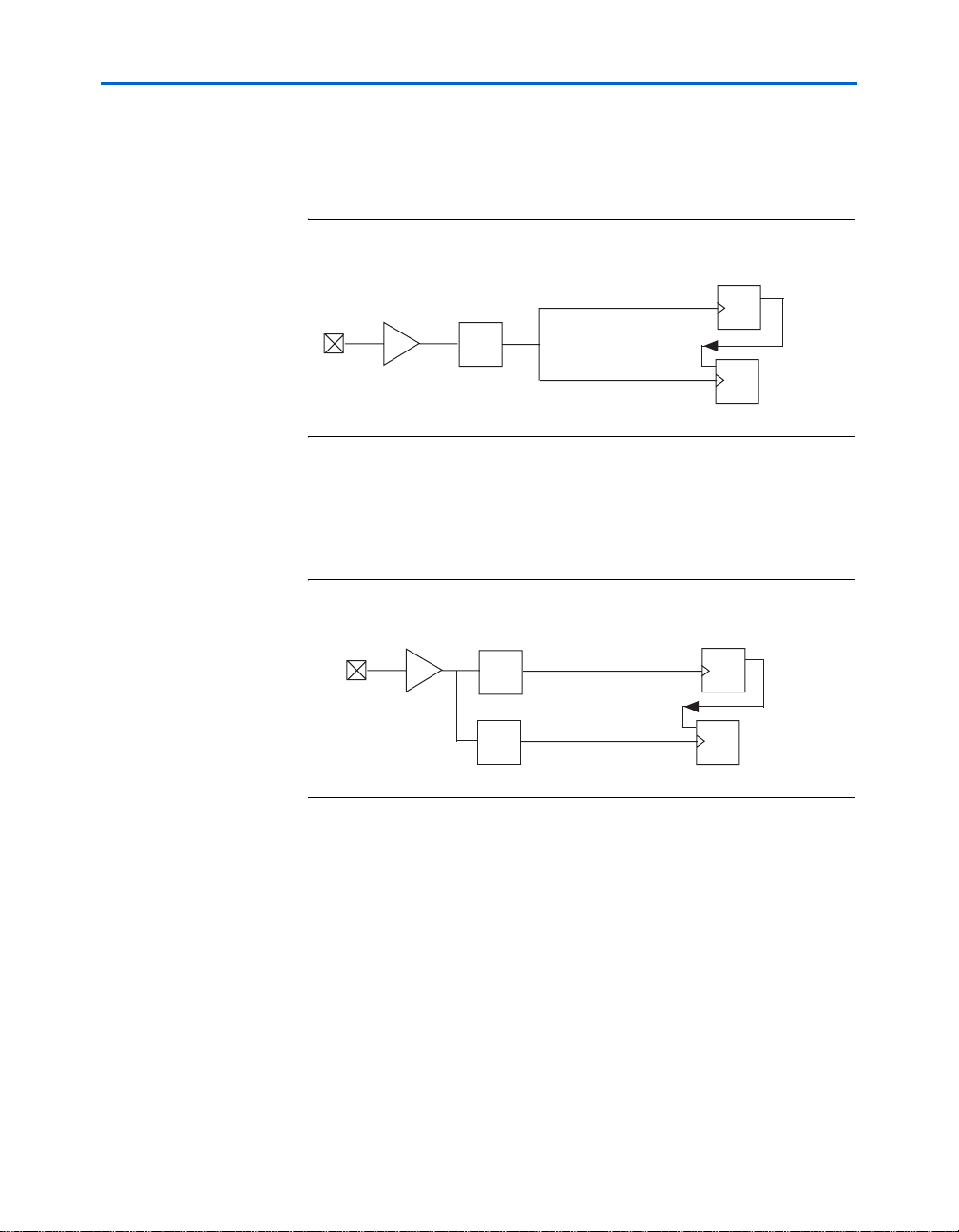
Inter-Clock Transfer
Inter-clock transfer occurs when the source and destination clocks come
from different PLLs and I/O clock pins, as shown in Figure 1–4.
Figure 1–4. Inter-Clock T ransfer
INBUF
PLL5
PLL9
CLK2
CLK7
Source
Clock
Destination
Register
Destinatio
Register
Altera Corporation 1–5
August 2007 HardCopy II Clock Uncertainty Calculator User Guide
Page 12
General Description
n
Register
A
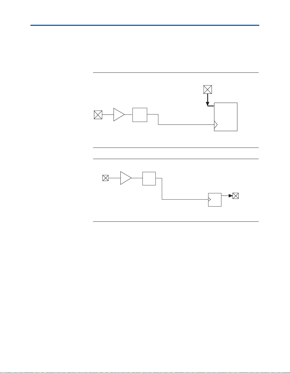
I/O Transfer
I/O transfer occurs when the clock transfer from an off-chip to the
destination clock (input) or, clock transfer from the source clock to an
off-chip (output), as shown in Figures 1–5 and 1–6.
Figure 1–5. Input Transfer
DATA
Destinatio
Register
INBUF
PLL10
CLK5
Destination
Clock
Figure 1–6. Output Transfer
PLL7
INBUF
CLK2
Source
Clock
DAT
Source
Refer to Appendix A, Clock Transfer Examples for more examples of
clock transfer cases.
Clock Uncertainty Calculator Spreadsheet
The clock uncertainty calculator spreadsheet consists of three parts:
■ Instructions
■ Clock uncertainty calculator
■ Advanced Clock Uncertainty (ACU) calculator
Instructions
The clock uncertainty calculator spreadsheet is a Microsoft Excel-based
file. The first worksheet provides quick-start instructions for using the
calculators. Both the clock uncertainty and advanced clock uncertainty
1–6 Altera Corporation
HardCopy II Clock Uncertainty Calculator User Guide August 2007
Page 13

About HardCopy II Clock Uncertainty Calculator
calculators require the PLL settings summary file,
pll_settings_summary.txt, as input data to calculate the clock uncertainty
values.
Clock Uncertainty Calculator
The clock uncertainty calculator is on the second worksheet. It operates
with a single green button and supports all designs, except designs with
a cascading PLL structure. When the clock uncertainty values are
calculated, they are displayed on the spreadsheet, and simultaneously
written to a text file, CU_Values.txt. The clock uncertainty values are for
worst-case scenarios, and account for I/O buffer noise, clock network
noise, core noise, PLL jitter, and static phase error.
Advanced Clock Uncertainty Calculator
The advanced clock uncertainty calculator is different than the clock
uncertainty calculator. The clock uncertainty values from the advanced
clock uncertainty calculator are considered more precise than the clock
uncertainty calculator, because it accounts for each dedicated PLL’s
utilization within the design. The advanced clock uncertainty calculator
requires the input of PLLs’ indices for both the source and destination
clock. Therefore, entering the PLLs’ indices on the advanced clock
uncertainty calculator should be relied on for both the PLL_Names.txt file
and the clock transfer report to generate the clock uncertainty values.
Also, you should use this calculator if there are cascading PLLs in the
design. After clock uncertainty calculation, the clock uncertainty values
are displayed on the spreadsheet and written to a text file,
CU_Advanced_Values.txt.
Both the advanced clock uncertainty and clock uncertainty calculators
can calculate and display the setup and hold uncertainty results for
different types of clock transfers. You can apply these clock uncertainty
constraints to model jitter and noise to ensure integrity with clock signals.
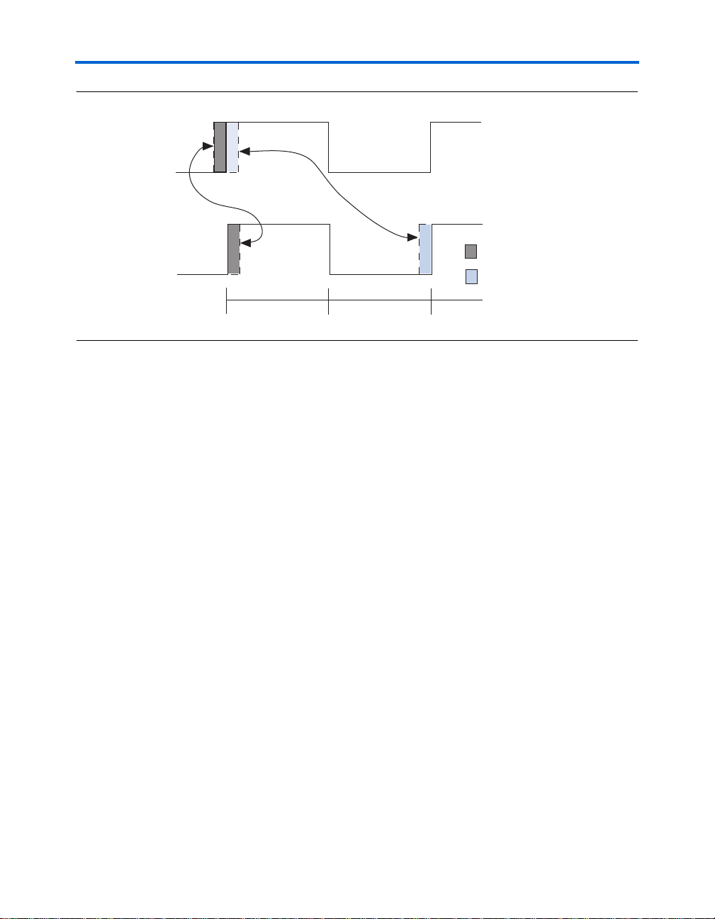
When a clock uncertainty constraint exists for a clock signal, the
TimeQuest Timing Analyzer performs the most conservative setup and
hold checks. For a clock setup check, the setup uncertainty is subtracted
from the data time requirement. For the clock hold check, the hold
uncertainty is added to the data time requirement. Figure 1–7 on page 1–8
shows examples of clock sources with a clock setup uncertainty applied
and clock sources with clock hold uncertainty applied.
Altera Corporation 1–7
August 2007 HardCopy II Clock Uncertainty Calculator User Guide
Page 14
General Description
S
D
0.0 ns
ty
ty
Figure 1–7. Clock Uncertainty Set-up and Hold Check
ource
Clock
estination
Clock
Clock hold check
with uncertainty
5.0 ns 10.0 ns
To obtain the clock uncertainty values from HardCopy II devices, you
should use the Altera HardCopy II Clock Uncertainty Calculator which
consists of the Tcl-based script for obtaining the PLL setting summary
and the Microsoft Excel-based spread sheet of clock uncertainty
calculators. Both utilities are packaged in the Altera HardCopy II Clock
Uncertainty Calculator, which is available on the Altera web
site (www.altera.com).
Clock steup check
with uncertainty
Clock Hold Uncertain
Clock Setup Uncertain
1–8 Altera Corporation
HardCopy II Clock Uncertainty Calculator User Guide August 2007
Page 15
Chapter 2. Launching the
HardCopy II Clock
Uncertainty Calculator
Release Information
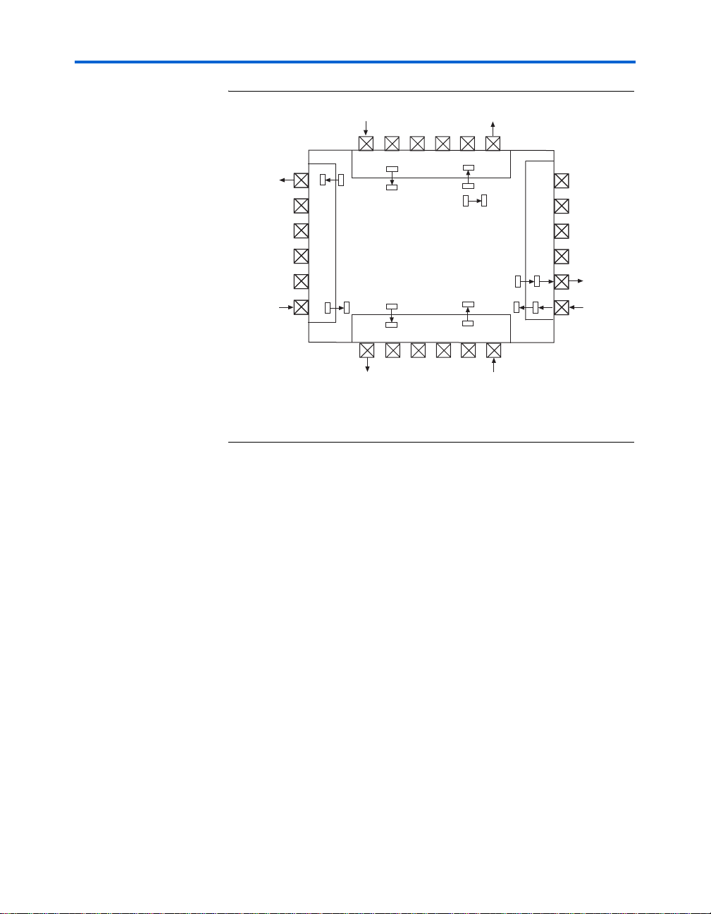
Device Family Support
Table 2–1 provides information about the version of HardCopy® II Clock
Uncertainty Calculator spreadsheet docu m ented in this user guide.
Table 2–1. HardCopy II Clock Uncertainty Calculator Spreadsheet Version
Device Family
HardCopy II 2.2 and later
The HardCopy II Clock Uncertainty Calculator supports the following
HardCopy II devices in Commercial and Industry temperature ranges:
■ HC240
■ HC230
■ HC220
■ HC210
■ HC210W (Use HC210 clock uncertainty value for HC210W)
The HardCopy II Clock Uncertainty Calculator was developed for
calculating the clock uncertainties caused by clock jitter, duty cycle
distortion, and phase shift error. With different interfaces of the clock
transferring on the chip, you may have different outcomes for the clock
uncertainty.
As shown in Figure 2–1, the HardCopy II Clock Uncertainty Calculator
covers clock transfer at the following locations:
HardCopy II Clock Uncertainty
Calculator Spreadsheet Version
■ Within core
■ Between the core and I/O
■ Between the core and SERDES/DDR blocks
Altera Corporation 2–1
Page 16
System and Software Requirements
Figure 2–1. HardCopy II Clock Uncertainty Calculator Coverage
Note to Figure 2–1:
(1) Transfer covered by DTW.
(2) Transfer covered by SERDES.
(3) Transfer covered by Altera HardCopy II Clock Uncertainty Calculator.
(2)
DDR (1)
S
E
R
D
E
S
CORE
HC230
DDR (1)
I
O
(3)
System and
The Altera® HardCopy II Clock Uncertainty Calculator spreadsheet
requires the following hardware and software:
Software
Requirements
2–2 Altera Corporation
HardCopy II Clock Uncertainty Calculator User Guide
■ A PC running the Windows NT/2000/XP operating system
■ Microsoft Office 2003 SP-1 or higher
■ Quartus
®
II software version 6.0 or higher
Page 17

Launching the HardCopy II Clock Uncertainty Calculator
Download and Install the HardCopy II Clock Uncertainty Calculator
The HardCopy II Clock Uncertainty Calculator includes a Tcl script for
PLL extraction and a clock uncertainty calculator spreadsheet, and is
available from the Altera web site (www.altera.com). After reading the
terms and conditions, and clicking I Agree, you can download the
package in .zip format to your hard drive.
Installation of HardCopy II Clock Uncertainty Calculator
After you download the .zip file of the HardCopy II Clock Uncertainty
Calculator package, unzip the file to extract the following files:
■ get_pll.tcl
■ HCII_CU_Calculator.Rev<version number>.xls
Copy or move these two files into the design’s Quartus II working
directory.
Running the Clock Uncertainty Calculator Flow
This section provides detailed procedures for the HardCopy II Clock
Uncertainty Calculator flow. It includes PLL extraction, clock transfer
report, and instructions for running the HardCopy II Clock Uncertainty
Calculator spreadsheet.
PLL Settings Summary Extraction
Before starting the PLL settings summary extraction, you should have the
generated FPGA design database ready in the Quartus II software. Even
if your design does not contain any PLLs, you must still run the design
through the Quartus II software. PLL settings summa ry extraction
requires the Tcl script, get_pll.tcl, within the working directory.
Syntax
Use the following syntax for the PLL settings summary extraction:
$QUARTUS_HOME/bin/quartus_sh –t get_pll.tcl
<project_name>
where $QUARTUS_HOME is the installation directory of the Quartus II
software.
Altera Corporation 2–3
HardCopy II Clock Uncertainty Calculator User Guide
Page 18
Running the Clock Uncertainty Calculator Flow
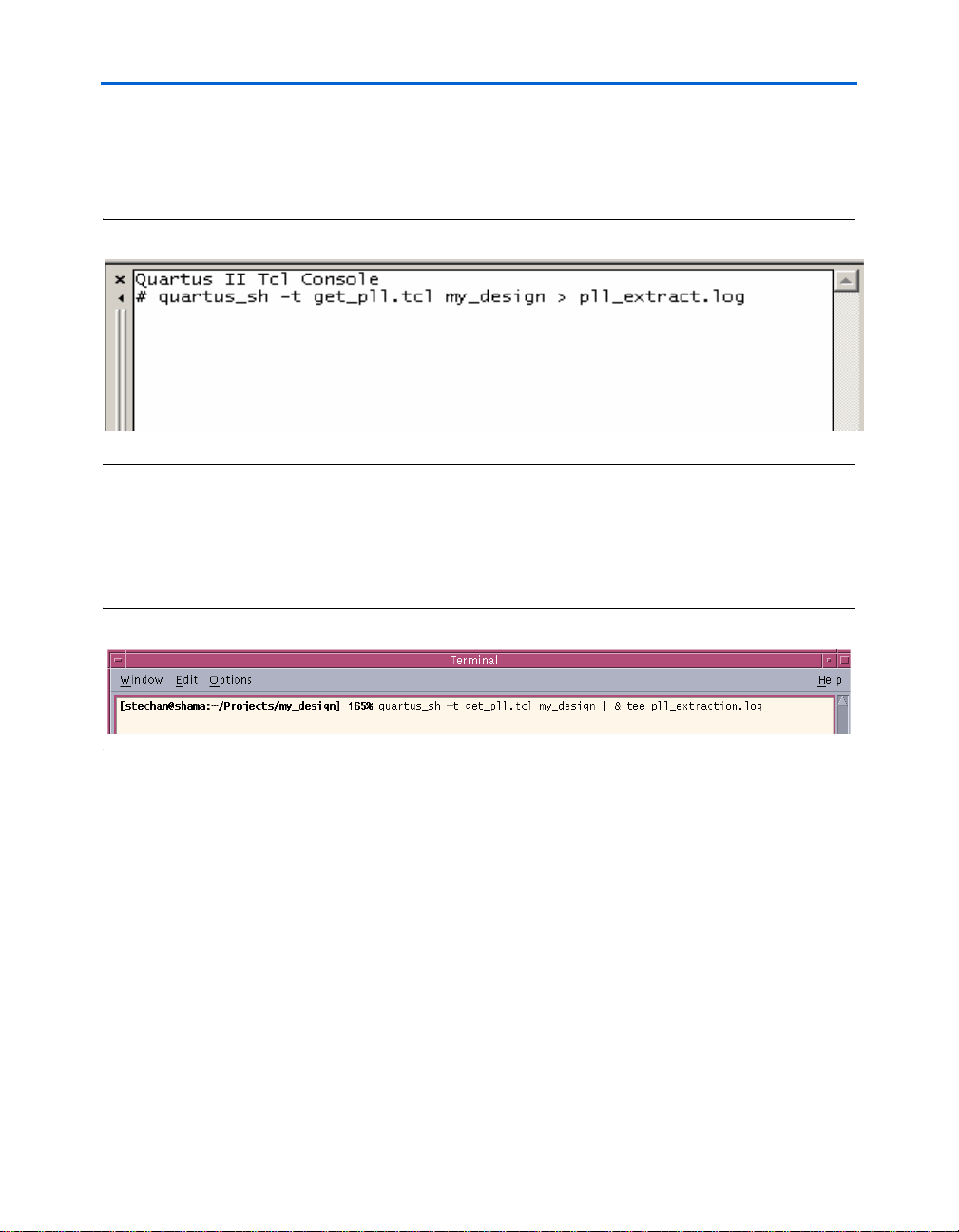
Running get_pll.tcl on the Quartus II Tcl Console
Figure 2–2 shows the PLL settings summary extraction using the
Quartus II software.
Figure 2–2. Example for Getting PLL Settings on the Quartus II Tcl Console
Running get_pll.tcl on the Command Line or UNIX
Figure 2–3 shows the PLL settings summary extraction using the
command line or UNIX.
Figure 2–3. Example for Acquiring PLL Settings on UNIX Prompt
After you complete the PLL extraction, you will have generated two files,
pll_settings_summary.txt and PLL_Names.txt, in the working directory.
You should also check the log file to confirm that the PLL extraction job
has completed without any errors.
The pll_settings_summary.txt file contains PLL indices, PLL names,
feedback counter (M) values, charge pump current, loop filter resistances,
voltage controlled oscillator (V
) frequency, and phase frequency
CO
detector frequency, that are required for running the clock uncertainty
calculators. Y o u will need pll_settings_summary.txt to continue the
clock uncertainty calculator spreadsheet.
2–4 Altera Corporation
HardCopy II Clock Uncertainty Calculator User Guide
Page 19
Launching the HardCopy II Clock Uncertainty Calculator
1 If the above parameters in pll_settings_summary.txt changed
during the HardCopy II design development, you should re-run
the HardCopy II Clock Uncertainty Calculator and update the
clock uncertainty constraints.
PLL_Names.txt is an optional file for the clock uncertainty calculator
spreadsheet. However, it provides useful information when using the
advanced clock uncertainty calculator worksheet, as it helps to identify
the corresponding PLL index for each PLL name.
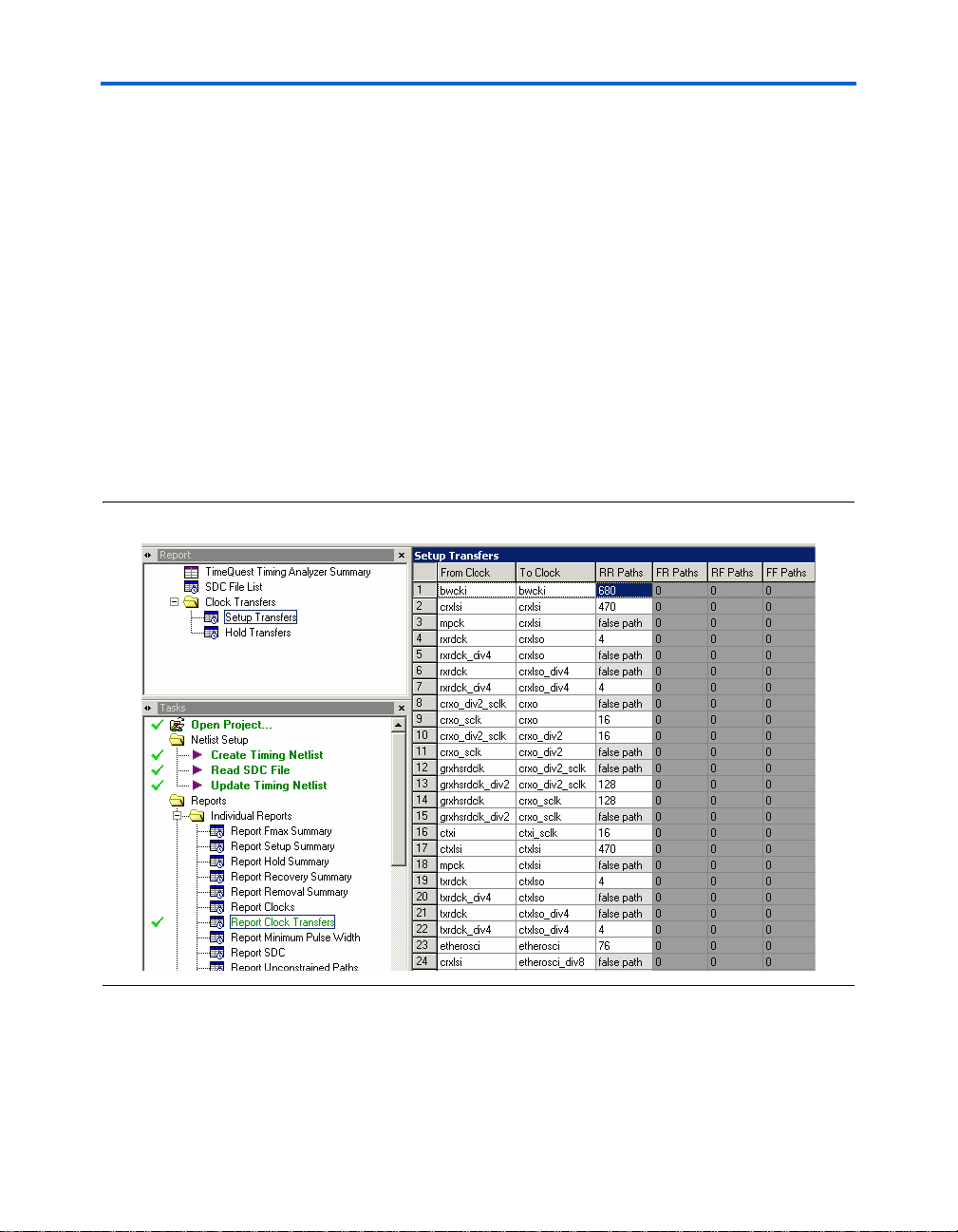
Report Clock Transfers Using the TimeQuest Timing Analyzer
After you confirm that all clock assignments are correct, run
report_clock_transfers, or, in the Tasks pane on the TimeQuest
Timing Analyzer’s GUI, double-click Report Clock Transfers. The
command generates a summary table with the number of paths between
each clock domain, as shown in Figure 2–4.
Figure 2–4. TimeQuest Timing Analyzer's Report Clock Transfers
Y ou can also use the report_clock_transfers command to generate
a report that details all clock-to-clock transfers in the design, as s hown in
Figure 2–5 on page 2–6. A clock-to-clock transfer is reported if a path
exists between two registers measured by two different clocks.
Altera Corporation 2–5
HardCopy II Clock Uncertainty Calculator User Guide
Page 20

Running the Clock Uncertainty Calculator Flow
Information such as the number of destinations and sources is also
reported. Ignore these clock transfers for clock uncertainty if they ar e set
as false paths.
1 Clock transfers must be verified before you specify the clock
uncertainty.
Figure 2–5. Command of Report Clock Transfers for the TimeQuest Timing Analyzer
f Refer to the Quartus II Handbook for more information about
report_clock_transfer.
Run HardCopy II Clock Uncertainty Calculator Spreadsheet
From the design’s working directory, browse to the Microsoft Excel file
HCII_CU_Calculator.Rev<version number>.xls, which is the
spreadsheet for the HardCopy II Clock Uncertainty Calculator. Open the
file to see the three worksheets in this file. The first worksheet provides
instructions on how to use the clock uncertainty calculator. You should
read the terms and conditions at the end of this page before you use the
clock uncertainty calculator.
Using the Clock Uncertainty Calculator
The second worksheet contains the clock uncertainty calculator. On this
worksheet, notice the "N/A" entries (Figure 2–6) indicating there is no
clock uncertainty calculation. If there are numbers on the worksheet from
aprevious calculation, click the yellow Reset Table button to clear all
previous clock uncertainty results.
2–6 Altera Corporation
HardCopy II Clock Uncertainty Calculator User Guide
Page 21

Launching the HardCopy II Clock Uncertainty Calculator
Figure 2–6. HardCopy II Clock Uncertainty Calculator without Calculation
To start the calculation of clock uncertain ty values, click the green
Calculate Clock Uncertainty Values button. All setup and hold clock
uncertainty values for different clock transfe r s are displayed in
picosecond (ps) units.
The clock uncertainty values are contained in the CU_Values.txt file. If
you have a previously-existing clock uncertainty value file generated by
the clock uncertainty calculator, the file will be renamed to be
CU_Values.txt.old.
Figure 2–7. HardCopy II Clock Uncertainty Calculator with Calculation
Altera Corporation 2–7
HardCopy II Clock Uncertainty Calculator User Guide
Page 22

Running the Clock Uncertainty Calculator Flow
Using the Advanced Clock Uncertainty Calculator
The third worksheet contains the advanced clock uncertianty calculator.
From Step 1. Enter PLL Information, as shown in Figure 2–8, enter the
PLL indices for source clock and destination cl ock before you click the
green Step 2. Calculate Clock Uncertainty Values button.
Under the Source Clock and Destination Clock cells in Figure 2–8, there
are first PLL and second PLL cells on the worksheet, which means the
advanced clock uncertianty calculator supports designs with cascaded
PLLs and each clock path has a maximum of two PLLs cascaded.
If there is no PLL in the design, you still must enter "0" for the first PLL
cell on the worksheet.
As in the advanced clock uncertianty calculator, click the yellow Reset
Table button to clear all previous clock uncertainty r esults. You can enter
notes for reference in the last cell of the table. The advanced clock
uncertianty calculator supports up to 200 clock transfer combinations.
Figure 2–8. HardCopy II Advanced Clock Uncertainty Calculator without Calculation
Step 1. Enter PLL Information
Source Clock Destination Clock Intra-clock Inter-Clock IO Transfer
1st PLL 2nd PLL 1st PL L 2nd PLL Setup (ps) Hold (ps) Setup (ps) Hold (ps) Setup (ps) Hold (ps)
1
2
3
4
5
Before beginning the calculation of clock uncertainty values, refer to the
clock transfer report and PLL_Names.txt. The clock transfer report shows
all clock-to-clock transfers in detail and PLL_Names.txt provides the
corresponding PLL index for each PLL name. Figure 2–9 show how to
enter the PLL indices for the advanced clock uncertianty calculator:
Step 3. Read Clock Uncertainty Values
Step 2. Calculate Clock
Step 2. Calculate Clock
Uncertainty Values
Uncertainty Values
Reset Table
Reset Table
MessagesTransfer
Enter User's Notes
(Optional)
2–8 Altera Corporation
HardCopy II Clock Uncertainty Calculator User Guide
Page 23

Launching the HardCopy II Clock Uncertainty Calculator
Refer to the highlighted column in Figure 2–9 of the clock transfer report
and PLL_Names.txt for the following procedures:
1. From the clock transfer report, trace the pin or port under "From
Clock".
For example, altpll0:PLL0|altpll"altpll_component|_clk1.
2. Refer to the PLL_Name.txt file to and see what the PLL index is
associated to.
For example, altpll0:PLL0|altpll"altpll_component associates to
PLL_2.
3. From the clock transfer report, trace the pin or port under "To
Clock".
For example, altpll0:PLL1|altpll"altpll_component|_clk0.
4. Refer to the PLL_Name.txt file in Figure 2–9 to see what the PLL
index associated to.
For example, altpll0:PLL1|altpll"altpll_component associates to
PLL_1.
You now know the source clock from PLL_2 and the destination
clock from PLL_1.
5. Enter 2 and 1 into the first PLL cell of the source clock and the
destination clock, respective ly, as shown in Figure 2–10 on
page 2–10.
Figure 2–9. Clock Transfer Report and PLL_Names.txt
Altera Corporation 2–9
HardCopy II Clock Uncertainty Calculator User Guide
Page 24

Running the Clock Uncertainty Calculator Flow
Figure 2–10 shows a detailed view of the advanced clock uncertianty
calculator spreadsheet. It is important that the first PLL be an integer
number even if there is no PLL involved in the clock transfer. After
having the clock transfer between the different PLLs, ente r the PLL index
with respect to the PLL in the spreadsheet, as shown on Figure 2–10.
Figure 2–10. Detailed View of the Advanced Clock Uncertianty Calculator
f For more examples of how to enter th e source clock and destination
clock components, refer to Appendix A, Clock Transfer Examples.
After you complete all entries for the source and destination clock
components, click the Step 2. Calculate Clock Uncertainty Values
button. All setup and hold clock uncertainty values for the different clock
transfers are displayed in picoseconds.
You now have the all the clock uncertainty values in the
CU_Values_Advanced.txt file. If you have a previously existing clock
uncertainty value file generated by the advanced clock uncertianty
calculator , the file will be renamed to be CU_Values_Advanced.txt.old.
Figure 2–11. HardCopy II Advanced Clock Uncertainty Calculator with Calculation
Step 2. Calculate Clock
Step 2. Calculate Clock
Uncertainty Values
Uncertainty Values
Rese t Table
Reset Table
Step 1. Enter PLL Information
Source Clock Destination Clock Intra-clock Inter-Clock IO Transfer
1st PLL 2nd PL L 1s t PLL 2nd PLL Setup (ps) Hold (p s) Setup (ps) Hold (ps) Setup (ps) Hold (ps)
1 00 200 50 350 350 180 180
44
2
04 N/A N/A
3
4
11 0 N/A N/A
5 10 11 N/A N/A 300 200 N/A N/ A
100 50
2–10 Altera Corporation
HardCopy II Clock Uncertainty Calculator User Guide
Step 3. Read Clock Uncert ainty Values
N/A N/A N/A N/A
320 290 150 120
270 330 100 150
MessagesTransfer
Enter User's Notes
(Optional)
Page 25

Launching the HardCopy II Clock Uncertainty Calculator
1 If the clock uncertainty values exceed 500 ps, they will be
highlighted on the spreadsheet. The values provided are based
on the general design’s maximum clock uncertainty. You must
verify whether the clock uncertainty causes the timing closure
for the design. Redesign may be necessary if you must r educe
the clock uncertainty number to close timing.
Using the clock uncertainty or advanced clock uncertainty calculators
depends on the design’s timing requirement, the PLL structures, or both.
Create Clock Uncertainty Timing Constraints on a SDC
After you have the clock transfer report and clock uncertainty values, you
can start to create the clock uncertainty constraints file in SDC format. Use
the TimeQuest Timing Analyzer SDC File Editor to create a constraint
file.
Use the following syntax to set the clock uncertainty value:
set_clock_uncertainty [-fall_from <fall_from_clock>] [-fall_to
<fall_to_clock>] [-from <from_clock>] [-hold] [-rise_from
<rise_from_clock>] [-rise_to <rise_to_clock>] [-setup] [-to <to_clock>]
<uncertainty>
Refer to the highlighted column in Figure 2–12 of the clock transfer report
and clock uncertainty values for the following procedures:
1. From the clock transfer report, identify the transfer clock type of the
pair of source and destination clocks.
For example, from altpll0:PLL0|altpll"altpll_component|_clk0
(source clock) to altpll0:PLL0|altpll"altpll_component|_clk1
(destination clock), the trasfer clock type is Intra-Clock Transfer.
2. From the clock transfer report, identify the cell type of both source
and destination clock pins.
For example, both altpll0:PLL0|altpll"altpll_component|_clk0
(source clock) and altpll0:PLL0|altpll"altpll_component|_clk1
(destination clock) are the PLL's output clock pins.
3. Based on the step 1 and 2 information, refer to t he clock uncertainty
values to collect both setup and hold uncertainty values.
For example, Intra-Clock T ransfer and with PLL: Setup CU = 100 ps,
Hold CU = 50 ps.
Altera Corporation 2–11
HardCopy II Clock Uncertainty Calculator User Guide
Page 26

Running the Clock Uncertainty Calculator Flow
4. Create the clock uncertainty constraint on a SDC.
For example, set_clock_uncertainty –from
altpll0:PLL0|altpll"altpll_component|_clk0 \
-to altpll0:PLL0|altpll"altpll_component|_clk1 \-setup 0.100
set_clock_uncertainty –from
altpll0:PLL0|altpll"altpll_component|_clk0 \-to
altpll0:PLL0|altpll"altpll_component|_clk1 \-hold 0.050.
Figure 2–12. Clock Transfer Report and Clock Uncertainty Values
For more information about the clock transfer types, refer to Chapter 1,
About HardCopy II Clock Uncertainty Calculator. In addition, there are
examples of clock transfer types in Chapter A, Clock Transfer Examples
of this user guide.
2–12 Altera Corporation
HardCopy II Clock Uncertainty Calculator User Guide
Page 27

Chapter 3. Design Case
D
C
Exceptions
Multiple Clock
In real designs, there are some special cases for calculating clock
uncertainty values that require extra steps.
Uncertainty on a
Single Clock
Transfer
Figure 3–1. Circuit with Intra-Clock Transfer and I/O Interface
IN1
LK1
INBUF
Example 3–1. SDC Constraints for i/O
create_clock –name CLK1 –period 10 [get_ports {CLK1}]
create_clock –name VIRTUAL_CLK –period 10
set_input_delay –max –clock VIRTUAL_CLK 8.00 [get_ports {DIN1}]
set_input_delay –min –clock VIRTUAL_CLK 2.00 [get_ports {DIN1}]
set_clock_uncertainty –from CLK1 –to CLK1 –setup 0.200
set_clock_uncertainty –from CLK1 –to CLK1 –hold 0.050
set_clock_uncertainty –from VIRTUAL_CLK1 –to CLK1 –setup 0.180
set_clock_uncertainty –from VIRTUAL_CLK1 –to CLK1 –hold 0.180
Figure 3–1 shows a design with both I/O transfer and intra-clock
transfer . In this case, there are two possible clock uncertainti es (I /O and
data paths) for the same clock transfer.
Clock T ransf er Type
Intra-Clock
Inter-Clock
I/O Interface
With PLL
Without PLL
With PLL
Without PLL
With PLL
Without PLL
Setup CU (ps) Hold CU (ps)
100
200
330
350
150
180 180
To set the clock uncertainty constraints correctly, you should create a
virtual clock for the circuit. The following code example shows the SDC
used to constrain the design, as shown in Figure 3–1:
50
50
330
350
150
Altera Corporation 3–1
Page 28

Various Clock Structures
Clock
n
Source
n
Various Clock
When a clock is generated in the core, additional clock uncertainty may
be introduced by the additional routing. The HardCopy
Structures
Uncertainty Calculator supports the following clock structures:
■ AND and MUX gated clocks
■ Clock divider
■ Ripple clock
■ Multiple clock networks
■ Multi-cycle clock
For each global and local clock network added to any of the examples in
Appendix A, clock uncertainty val ues should be increased by 25 ps. The
following examples are for intra-clock transfer with PLL; the same rules
apply for inter-clock transfer and I/O transfers, as well as for all cases not
involving PLLs.
Clock Gated in Core
In Figures 3–2 and 3–3, the source register is driven by an AND or MUX
gated clock, CLK2. Because the clock uncertainty calculator does not
account for the clock network on CLK2, you must add 25 ps on both the
setup and hold clock uncertainty values.
Figure 3–2. AND-Gated Clock for Intra-Clock Transfer
CLK1
PLL
CLK2
Source
Clock
®
II Clock
Source
Register
INBUF
CLK3
Destination
Destinatio
Register
Figure 3–3. MUX-Gated Clock for Intra-Clock Transfer
CLK1
PLL
INBUF
3–2 Altera Corporation
HardCopy II Clock Uncertainty Calculator User Guide
CLK2
CLK3
Clock
Destination
Clock
Source
Register
Destinatio
Register
Page 29

Clock Divider
n
C
Figure 3–4 shows an example of a clock divider for intra-clock transfer, in
which CLK1 is accounted for in the clock uncertainty calculator, but not
CLK2. Y ou should add 25 ps to both the setup and hold clock uncertainty
values.
Figure 3–4. Clock Divider for Intra-Clock Transfer
CLK1
PLL
CLK2
Design Case Exceptions
Source
Clock
Source
Register
INBUF
CLK3
Destination
Clock
Destinatio
Register
Ripple Clock
Figure 3–5 shows a ripple clock as an intra-cloc k transfer example. A
ripple clock is similar to a divided clock, but uses a different calculation
to account for extra clock uncertainty value.
CLK0 is accounted for by the clock uncertainty calculator, but not CLK1
and CLK2. You need to add 25 ps uncertainty for the CLK1 network and
also add 25 ps uncertainty for the CLK2 network. Therefore, you should
add 50 ps on both setup and hold clock uncertainty for the example
shown in Figure 3–5.
Figure 3–5. Ripple Clock for Intra-Clock Transfer
reg_c reg_d
CLK1
CLK2
clk_a
LK0
clk_b
CLK1
Altera Corporation 3–3
HardCopy II Clock Uncertainty Calculator User Guide
Page 30

Various Clock Structures
er
n
Multiple Clock Networks
Figure 3–6 shows an example of multiple clock networks.
Figure 3–6. Multiple Clock Networks
CLK1
PLL
INBUF
The CLK1 and CLK4 networks are accounted for by the clock unce rtainty
calculator, but the CLK2, CLK3, CLK5, and CLK6 networks are ignored.
Therefore, you should add 25 ps for each ignored clock network to the
setup and hold clock uncertainty for the example in Figure 3–6.
Multi-Cycle Clock
The multi-cycle clock occurs when there is a delay (Δt) that is greater than
the clock period between the source register and destination register.
Refer to Figure 1–7. The default hold clock uncertainty value is
considered that the source clock and destination clock are on the same
edge.
CLK4
CLK2
CLK5
CLK3
CLK6
Source
Clock
Destination
Clock
Source
Regist
Destinatio
Register
When the multi-cycle path timing exception is set, you need pay attention
for the hold clock uncertainty of Intra-clock transfers since the possible
hold checks are not at the launch edge for both source and destination
clock due to the extra delay (Δt) on the data path.
3–4 Altera Corporation
HardCopy II Clock Uncertainty Calculator User Guide
Page 31

Figure 3–7. Multi-Cycle Clock
Possible Hold Checks
INBUF
PLL
CLK1
CLK2
Source
Register
R1
Design Case Exceptions
Destination
tΔ
Register
R2
Launch
Edge
E0
Capture
Edge
E1 E2 E3
E4
Setup Check
In the example shown in Figure 3–7, the multi-cycle path timing
exception is set and the hold margin is not checked at the launch clock
edge, in other words, the hold margin is checked at E1, E2, or E3 edge.
You should use the setup clock uncertainty value from clock uncertainty
calculator for hold clock uncertainty constraints.
Figure 3–8 shows the clock uncertainty result from the schematic circuit.
The setup clock uncertainty is 100 ps, and the hold clock uncertainty is
50 ps. If the hold margin is on E1, E2, or E3, use the following example:
set_clock_uncertainty -from CLK1 -to CLK2 -hold 100ps
If the hold margin is on E0, use the following example:
set_clock_uncertainty -from CLK1 -to CLK2 -hold 50ps
Altera Corporation 3–5
HardCopy II Clock Uncertainty Calculator User Guide
Page 32

Various Clock Structures
Figure 3–8. Clock Uncertainty from a Schematic Circuit
Clock Transfer Type
Intra-Clock
Inter-Clock
I/O Interface
With PLL
Without PLL
With PLL
Without PLL
With PLL
Without PLL
Setup CU (ps) Hold CU (ps)
100
200
330
350
150
180
50
50
330
350
150
180
3–6 Altera Corporation
HardCopy II Clock Uncertainty Calculator User Guide
Page 33

Appendix A. Clock Transfer
er
Examples
This appendix provides clock transfer examples for the HardCopy® II
Clock Uncertainty Calculator.
Intra-Clock
This section provides clock transfer examples for an intra-clock domain
with at least one PLL.
Domain with
PLL
Figure A–1. Intra-Clock Domain with a Shared PLL Output
INBUF
Figure A–1 shows an example of a clock-pair = CLK11 to CLK11
CLK11
PLL9
CLK11
Table A–1 shows input of the PLL index for Figure A–1, with respect to
the source and destination clocks.
Table A–1. Location of Input PLLs
Source
Clock
Destination
Clock
Source
Regist
Destination
Register
Source Clock Destination Clock
1st PLL 2nd PLL 1st PLL 2nd PLL
9—9—
Altera Corporation A–1
Page 34

Intra-Clock Domain with PLL
er
Figure A–2 shows an example of a clock-pair = CLK5 to CLK6
Figure A–2. Intra-Clock Domain with Two PLL Outputs
CLK5
PLL11
INBUF
CLK6
Table A–2 shows input of the PLL index for Figure A–2, with respect to
the source and destination clocks.
Table A–2. Location of Input PLLs
Source Clock Destination Clock
Source
Clock
Destination
Clock
Source
Regist
Destination
Register
1st PLL 2nd PLL 1st PLL 2nd PLL
11 — 11 —
A–2 Altera Corporation
HardCopy II Clock Uncertainty Calculator User Guide
Page 35

Intra-Clock
er
This section provides clock transfer examples for an intra-clock domain
without a PLL.
Domain without
PLL
Figure A–3. Intra-Clock Domain without a PLL
Figure A–3 shows an example of a clock-pair = CLK1 to CLK1
CLK1
Source
Clock
Source
Regist
INBUF
Destination
CLK1
Destination
Clock
Register
Table A–3 shows input of the PLL index for Figure A–3, with respect to
the source and destination clocks.
1 If no PLL exists, enter “0” for both the source and destination
clocks.
Table A–3. Location of Input PLLs
Source Clock Destination Clock
1st PLL 2nd PLL 1st PLL 2nd PLL
0—0—
Altera Corporation A–3
HardCopy II Clock Uncertainty Calculator User Guide
Page 36

Inter-Clock Domain with PLL
er
Inter-Clock
This section provides clock transfer examples for an inter -c loc k domain
with a PLL.
Domain with
PLL
Figure A–4. Inter-Clock Domain with a PLL on the Destination Clock
INBUF
Figure A–4 shows an example of a clock-pair = CLK3 to CLK5
CLK3
PLL7
CLK5
Destination
Table A–4 shows input of the PLL index for Figure A–4, with respect to
the source and destination clocks.
Table A–4. Location of Input PLLs
Source
Clock
Clock
Source
Regist
Destination
Register
Source Clock Destination Clock
1st PLL 2nd PLL 1st PLL 2nd PLL
0—7—
A–4 Altera Corporation
HardCopy II Clock Uncertainty Calculator User Guide
Page 37

Figure A–5 shows an example of a clock-pair = CLK8 to CLK10
er
Figure A–5. Inter-Clock Domain with a PLL on the Source Clock
PLL3
INBUF
CLK8
CLK10
Table A–5 shows input of the PLL index for Figure A–5, with respect to
the source and destination clocks.
Table A–5. Location of Input PLLs
Source Clock Destination Clock
1st PLL 2nd PLL 1st PLL 2nd PLL
3—0—
Source
Clock
Destination
Clock
Source
Regist
Destination
Register
Altera Corporation A–5
HardCopy II Clock Uncertainty Calculator User Guide
Page 38

Inter-Clock Domain with PLL
er
Figure A–6 shows an example of a clock-pair = CLK2 to CLK7
Figure A–6. Inter-Clock Domain with Two PLLs
PLL5
INBUF
PLL9
Table A–6 shows input of the PLL index for Figure A–6, with respect to
the source and destination clocks.
Table A–6. Location of Input PLLs
CLK2
CLK7CLK6
Source
Clock
Destination
Clock
Source
Regist
Destination
Register
Source Clock Destination Clock
1st PLL 2nd PLL 1st PLL 2nd PLL
5—9—
A–6 Altera Corporation
HardCopy II Clock Uncertainty Calculator User Guide
Page 39

Figure A–7 shows an example of a clock-pair = CLK3 to CLK9
er
Figure A–7. Inter-Clock Domain with Two Independent Clocks and a PLL on the Destination Clock
Source
Regist
Destination
Register
INBUF9
INBUF11
PLL4
CLK3
CLK9
Source
Clock
Destination
Clock
Table A–7 shows input of the PLL index for Figure A–7, with respect to
the source and destination clocks.
Table A–7. Location of Input PLLs
Source Clock Destination Clock
1st PLL 2nd PLL 1st PLL 2nd PLL
0—4—
Altera Corporation A–7
HardCopy II Clock Uncertainty Calculator User Guide
Page 40

Inter-Clock Domain with PLL
er
Figure A–8 shows an example of a clock-pair = CLK7 to CLK11
Figure A–8. Inter-Clock Domain with Two Independent Clocks and a PLL on the Source Clock
Source
Clock
Destination
Clock
Destination
Register
INBUF4
INBUF6
PLL12
CLK7
CLK11
Table A–8 shows input of the PLL index for Figure A–8, with respect to
the source and destination clocks.
Table A–8. Location of Input PLLs
Source
Regist
Source Clock Destination Clock
1st PLL 2nd PLL 1st PLL 2nd PLL
12 — 0 —
A–8 Altera Corporation
HardCopy II Clock Uncertainty Calculator User Guide
Page 41

Figure A–9 shows an example of a clock-pair = CLK9 to CLK12
er
Figure A–9. Inter-Clock Domain with Two Independent Clocks with a PLL
Source
Clock
Destination
Clock
INBUF3
INBUF2
PLL4
PLL2
CLK9
CLK12
Table A–9 shows input of the PLL index for Figure A–9, with respect to
the source and destination clocks.
Table A–9. Location of Input PLLs
Source Clock Destination Clock
1st PLL 2nd PLL 1st PLL 2nd PLL
4—2—
Source
Regist
Destination
Register
Altera Corporation A–9
HardCopy II Clock Uncertainty Calculator User Guide
Page 42

Inter-Clock Domain without PLL
er
Inter-Clock
This section provides clock transfer examples for an inter -c loc k domain
without a PLL.
Domain without
PLL
Figure A–10. Two Independent Clocks without a PLL
INBUF3
INBUF7
Figure A–10 shows an example of a clock-pair = CLK6 to CLK9
CLK6
CLK9
Table A–10 shows input of the PLL index for Figure A–10, with respect to
the source and destination clocks.
1 If no PLL exists, enter “0” for both the source and destination
clocks.
Source
Clock
Destination
Clock
Source
Regist
Destination
Register
Table A–10. Location of Input PLLs
Source Clock Destination Clock
1st PLL 2nd PLL 1st PLL 2nd PLL
0—0—
A–10 Altera Corporation
HardCopy II Clock Uncertainty Calculator User Guide
Page 43

I/O Interface
n
This section provides clock transfer examples for an I/O interface with at
least one PLL.
with PLL
Figure A–11 shows an example of a clock-pair = Off-chip to CLK5
Figure A–11. Input Interface with a PLL
DATA
Destinatio
Register
INBUF
PLL10
CLK5
Destination
Clock
Table A–11 shows input of the PLL index for Figure A–11, with r espect to
the source and destination clocks.
Table A–11. Location of Input PLLs
Source Clock Destination Clock
1st PLL 2nd PLL 1st PLL 2nd PLL
0—10—
Altera Corporation A–11
HardCopy II Clock Uncertainty Calculator User Guide
Page 44

I/O Interface without PLL
A
Figure A–12 shows an example of a clock-pair = CLK2 to Off-chip
Figure A–12. Output Interface with a PLL
PLL7
INBUF
Table A–12 shows input of the PLL index for Figure A–12, with respect to
the source and destination clocks.
Table A–12. Location of Input PLLs
1st PLL 2nd PLL 1st PLL 2nd PLL
DAT
CLK2
Source
Clock
Source
Register
Source Clock Destination Clock
7—0—
I/O Interface
This section provides clock transfer examples for an I/O interface
without a PLL.
without PLL
A–12 Altera Corporation
HardCopy II Clock Uncertainty Calculator User Guide
Page 45

Figure A–13 shows an example of a clock-pair = Off-chip to CLK8
n
A
Figure A–13. Input Interface without PLL
INBUF
Table A–13 shows input of the PLL index for Figure A–13, with respect to
the source and destination clocks.
1 If no PLL exists, enter “0” for both the source and destination
Table A–13. Location of Input PLLs
1st PLL 2nd PLL 1st PLL 2nd PLL
DATA
Destinatio
Register
CLK8
Destination
Clock
clocks.
Source Clock Destination Clock
0—0—
Figure A–14 shows an example of a clock-pair = CLK12 to Off-chip
Figure A–14. Output Interface without a PLL
Source
Clock
INBUF
CLK12
Source
Register
Altera Corporation A–13
HardCopy II Clock Uncertainty Calculator User Guide
DAT
Page 46

Intra-Clock Domain with Cascaded PLLs
er
Table A–14 shows input of the PLL index for Figure A–14, with respect to
the source and destination clocks.
1 If no PLL exists, enter “0” for both the source and destination
clocks.
Table A–14. Location of Input PLLs
1st PLL 2nd PLL 1st PLL 2nd PLL
0—0—
Source Clock Destination Clock
Intra-Clock
This section provides clock transfer examples for an intra-clock domain
with cascaded PLLs.
Domain with
Cascaded PLLs
Figure A–15. Intra-Clock Domain with Cascaded PLLs and Shared PLL Output
INBUF
Figure A–15 shows an example of a clock-pair = CLK7 to CLK7
Source
Clock
Destination
Clock
PLL5
CLK3
CLK7
PLL4
CLK7
Table A–15 shows input of the PLL index for Figure A–15, with respect to
the source and destination clocks.
Table A–15. Location of Input PLLs
Source
Regist
Destination
Register
Source Clock Destination Clock
1st PLL 2nd PLL 1st PLL 2nd PLL
5454
A–14 Altera Corporation
HardCopy II Clock Uncertainty Calculator User Guide
Page 47

Figure A–16 shows an example of a clock-pair = CLK6 to CLK7
er
Figure A–16. Intra-Clock Domain with Cascaded PLLs and 2 PLL Outputs
CLK6
CLK5
PLL9
INBUF
PLL11
CLK7
Destination
Table A–16 shows input of the PLL index for Figure A–16, with respect to
the source and destination clocks.
Table A–16. Location of Input PLLs
Source Clock Destination Clock
1st PLL 2nd PLL 1st PLL 2nd PLL
911911
Source
Clock
Clock
Source
Regist
Destination
Register
Altera Corporation A–15
HardCopy II Clock Uncertainty Calculator User Guide
Page 48

Inter-Clock Domain with Cascaded PLLs
er
Inter-Clock
This section provides clock transfer examples for an inter -c loc k domain
with cascaded PLLs.
Domain with
Cascaded PLLs
Figure A–17. Inter-Clock Domain with Cascaded PLLs on Destination Clock
INBUF
Figure A–17 shows an example of a clock-pair = CLK7 to CLK9
Source
Clock
Destination
Clock
PLL3
CLK2
PLL5
CLK7
CLK9
Table A–17 shows input of the PLL index for Figure A–17, with respect to
the source and destination clocks.
Table A–17. Location of Input PLLs
Source
Regist
Destination
Register
Source Clock Destination Clock
1st PLL 2nd PLL 1st PLL 2nd PLL
0—35
A–16 Altera Corporation
HardCopy II Clock Uncertainty Calculator User Guide
Page 49

Figure A–18 shows an example of a clock-pair = CLK4 to CLK7
er
Figure A–18. Inter-Clock Domain with Cascaded PLLs on the Source Clock
Source
CLK4
Destination
Clock
Clock
INBUF
CLK1
PLL9 PLL11
CLK7
Table A–18 shows input of the PLL index for Figure A–18, with respect to
the source and destination clocks.
Table A–18. Location of Input PLLs
Source Clock Destination Clock
1st PLL 2nd PLL 1st PLL 2nd PLL
910—
Source
Regist
Destination
Register
Altera Corporation A–17
HardCopy II Clock Uncertainty Calculator User Guide
Page 50

Inter-Clock Domain with Cascaded PLLs
er
Figure A–19 shows an example of a clock-pair = CLK5 to CLK7
Figure A–19. Inter-Clock Domain with Cascaded PLLs and One PLL Shared and the Second PLL on the
Destination Clock
Source
Regist
Destination
Register
INBUF
PLL7
CLK4
PLL9
CLK5
CLK7
Source
Clock
Destination
Clock
Table A–19 shows input of the PLL index for Figure A–19, with respect to
the source and destination clocks.
Table A–19. Location of Input PLLs
Source Clock Destination Clock
1st PLL 2nd PLL 1st PLL 2nd PLL
7—79
A–18 Altera Corporation
HardCopy II Clock Uncertainty Calculator User Guide
Page 51

Figure A–20 shows an example of a clock-pair= CLK7 to CLK8
er
Figure A–20. Inter-Clock Domain with Cascaded PLLs and One PLL Shared and the Second PLL on the
Source Clock
Source
Regist
Destination
Register
INBUF
CLK5
PLL3 PLL2
CLK8
CLK7
Destination
Source
Clock
Clock
Table A–20 shows input of the PLL index for Figure A–20, with respect to
the source and destination clocks.
Table A–20. Location of Input PLLs
Source Clock Destination Clock
1st PLL 2nd PLL 1st PLL 2nd PLL
323—
Altera Corporation A–19
HardCopy II Clock Uncertainty Calculator User Guide
Page 52

Inter-Clock Domain with Cascaded PLLs
er
Figure A–21 shows an example of a clock-pair = CLK8 to CLK11
Figure A–21. Inter-Clock Domain with Cascaded PLLs on the Destination Clock and One PLL on the Source
Clock
Source
Regist
Destination
Register
INBUF
CLK6
PLL3
PLL9
CLK8
CLK10 CLK10
PLL7
Source
Destination
Clock
Clock
Table A–21 shows input of the PLL index for Figure A–21, with respect to
the source and destination clocks.
Table A–21. Location of Input PLLs
Source Clock Destination Clock
1st PLL 2nd PLL 1st PLL 2nd PLL
3—97
A–20 Altera Corporation
HardCopy II Clock Uncertainty Calculator User Guide
Page 53

Figure A–22 shows an example of a clock-pair = CLK7 to CLK10
er
Figure A–22. Inter-Clock Domain with Cascaded PLLs on the Source Clock and One PLL on the Destination
Clock
Source
Regist
Destination
Register
INBUF
CLK2
PLL4
PLL11
CLK5
PLL6
CLK10
Source
CLK7
Destination
Clock
Clock
Table A–22 shows input of the PLL index for Figure A–22, with respect to
the source and destination clocks.
Table A–22. Location of Input PLLs
Source Clock Destination Clock
1st PLL 2nd PLL 1st PLL 2nd PLL
4611—
Altera Corporation A–21
HardCopy II Clock Uncertainty Calculator User Guide
Page 54

Inter-Clock Domain with Cascaded PLLs
er
Figure A–23 shows an example of a clock-pair = CLK3 to CLK6
Figure A–23. Inter-Clock Domain with Cascaded PLLs and One Shared and One on Source Clock and One on
Destination Clock
Source
Regist
Destination
Register
INBUF
PLL12
CLK2
CLK5
PLL3
PLL7
CLK3
CLK6
Source
Clock
Destination
Clock
Table A–23 shows input of the PLL index for Figure A–23, with respect to
the source and destination clocks.
Table A–23. Location of Input PLLs
Source Clock Destination Clock
1st PLL 2nd PLL 1st PLL 2nd PLL
12 3 12 7
A–22 Altera Corporation
HardCopy II Clock Uncertainty Calculator User Guide
Page 55

Figure A–24 shows an example of a clock-pair = CLK7 to CLK12
n
Clock
Figure A–24. Inter-Clock Domain with Cascaded PLLs and Two PLLs on the Sou rce Clock and Two PLLs on
the Destination Clock
Source
PLL4
CLK6
PLL3
CLK7
Clock
Source
Register
INBUF
PLL5
CLK11
PLL8
CLK12
Destinatio
Register
Destination
Table A–24 shows input of the PLL index for Figure A–24, with respect to
the source and destination clocks.
Table A–24. Location of Input PLLs
Source Clock Destination Clock
1st PLL 2nd PLL 1st PLL 2nd PLL
4358
Altera Corporation A–23
HardCopy II Clock Uncertainty Calculator User Guide
Page 56

Inter-Clock Domain with Cascaded PLLs
n
Figure A–25 shows an example of a clock-pair = CLK9 to CLK7
Figure A–25. Inter-Clock Domain with Two Independent Clocks and Cascaded PLLs on the Destination Clock
CLK9
INBUF2
Source
Clock
Source
Register
INBUF4
PLL10
CLK5
PLL11
CLK7
Destinatio
Register
Destination
Clock
Table A–25 shows input of the PLL index for Figure A–25, with respect to
the source and destination clocks.
Table A–25. Location of Input PLLs
Source Clock Destination Clock
1st PLL 2nd PLL 1st PLL 2nd PLL
0 — 10 11
A–24 Altera Corporation
HardCopy II Clock Uncertainty Calculator User Guide
Page 57

Figure A–26 shows an example of a clock-pair = CLK5 to CLK9
Source
n
Clock
Figure A–26. Inter-Clock Domain with Two Independent Clocks and Cascaded PLLs on the Source Clock
INBUF10
INBUF11
PLL12
CLK3
PLL2
CLK5
CLK9
Clock
Destination
Source
Register
Destinatio
Register
Table A–26 shows input of the PLL index for Figure A–26, with respect to
the source and destination clocks.
Table A–26. Location of Input PLLs
Source Clock Destination Clock
1st PLL 2nd PLL 1st PLL 2nd PLL
12 2 0 —
Altera Corporation A–25
HardCopy II Clock Uncertainty Calculator User Guide
Page 58

Inter-Clock Domain with Cascaded PLLs
n
Figure A–27 shows an example of a clock-pair = CLK2 to CLK10
Figure A–27. Inter-Clock Domain with Two Independent Clocks and Cascaded PLLs on the Destination Clock
and One PLL on the Source Clock
Source
Clock
Destination
Clock
Source
Register
Destinatio
Register
INBUF6
INBUF3
PLL10
PLL4
CLK9
PLL8
CLK2
CLK10
Table A–27 shows input of the PLL index for Figure A–27, with respect to
the source and destination clocks.
Table A–27. Location of Input PLLs
Source Clock Destination Clock
1st PLL 2nd PLL 1st PLL 2nd PLL
10 — 4 8
A–26 Altera Corporation
HardCopy II Clock Uncertainty Calculator User Guide
Page 59

Figure A–28 shows an example of a clock-pair = CLK8 to CLK9
n
Figure A–28. Inter-Clock Domain with Two Independent Clocks and Cascaded PLLs on Source Clock and One
PLL on the Destination Clock
Source
INBUF2
INBUF7
PLL4
PLL3
CLK5
PLL11
CLK8
CLK9
Clock
Destination
Clock
Source
Register
Destinatio
Register
Table A–28 shows input of the PLL index for Figure A–28, with respect to
the source and destination clocks.
Table A–28. Location of Input PLLs
Source Clock Destination Clock
1st PLL 2nd PLL 1st PLL 2nd PLL
4113—
Altera Corporation A–27
HardCopy II Clock Uncertainty Calculator User Guide
Page 60

Inter-Clock Domain with Cascaded PLLs
n
Figure A–29 shows an example of a clock-pair = CLK11 to CLK6
Figure A–29. Inter-Clock Domain with Two Independent Clocks and Cascaded PLLs on Both Source and
Destination Clocks
Source
INBUF3
INBUF4
PLL5
PLL4
CLK10
CLK5
PLL9
PLL3
CLK11
CLK6
Clock
Destination
Clock
Source
Register
Destinatio
Register
Table A–29 shows input of the PLL index for Figure A–29, with respect to
the source and destination clocks.
Table A–29. Location of Input PLLs
Source Clock Destination Clock
1st PLL 2nd PLL 1st PLL 2nd PLL
5943
A–28 Altera Corporation
HardCopy II Clock Uncertainty Calculator User Guide
Page 61

I/O Interface
n
This section provides clock transfer examples for an I/O interface with
cascaded PLLs.
with Cascaded
PLLs
Figure A–30. Input Interface with Cascaded PLLs
Figure A–30 shows an example of a clock-pair = Off-chip to CLK8
DATA
INBUF
PLL9
CLK3
PLL7
CLK8
Destination
Clock
Destinatio
Register
Table A–30 shows input of the PLL index for Figure A–30, with respect to
the source and destination clocks.
Table A–30. Location of Input PLLs
Source Clock Destination Clock
1st PLL 2nd PLL 1st PLL 2nd PLL
0—97
Altera Corporation A–29
HardCopy II Clock Uncertainty Calculator User Guide
Page 62

I/O Interface with Cascaded PLLs
A
Source
Figure A–31 shows an example of a clock-pair = CLK6 to Off-chip
Figure A–31. Output Interface with Cascaded PLLs
INBUF
PLL10
CLK5
PLL2
CLK2
Clock
DAT
Source
Register
Table A–31 shows input of the PLL index for Figure A–31, with respect to
the source and destination clocks.
Table A–31. Location of Input PLLs
Source Clock Destination Clock
1st PLL 2nd PLL 1st PLL 2nd PLL
10 2 0 —
A–30 Altera Corporation
HardCopy II Clock Uncertainty Calculator User Guide
 Loading...