

Page 1

HardCopy Series Handbook, Volume 1
101 Innovation Drive
San Jose, CA 95134
www.alter a.com
Preliminary Information
H5V1-4.5
Page 2

Copyright © 2008 Altera Corporation. All rights reserved. Altera, The Programmable Solutions Company, the stylized Altera logo, specific device designations, and all other words and logos that are identified as trademarks and/or service marks are, unless noted otherwise, the trademarks and
service marks of Altera Corporation in the U.S. and other countries. Mentor Graphics and ModelSim are registered trademarks of Mentor Graphics
Corporation. All other product or service names are the property of their respective holders. Altera products are protected under numerous U.S. and
foreign patents and pending applications, maskwork rights, and copyrights. Altera warrants performance of its semiconductor products to current
specifications in accordance with Altera's standard warranty, but reserves the right to make changes to any products and services at any time without
notice. Altera assumes no responsibility or liability arising out of the application or use of any information, product, or service described herein except as expressly agreed to in writing by Altera Corporation. Altera customers are advised to obtain the latest
version of device specifications before relying on any published information and before placing orders for products or services
.
ii Altera Corporation
Preliminary
Page 3

Contents
Chapter Revision Dates ........................................................................... ix
About this Handbook ............................................................................... xi
How to Contact Altera ........ ..................................................................................................................... xi
Typographic Conventions ....................................................................................................................... xi
Section I. HardCopy Stratix Device Family Data Sheet
Revision History .................................................................................................................................... 1–1
Chapter 1. Introduction to HardCopy Stratix Devices
Introduction ............................................................................................................................................ 1–1
Features ................................................................................................................................................... 1–2
Document Revision History ............................................ ..................................................................... 1–4
Chapter 2. Description, Architecture, and Features
Introduction ............................................................................................................................................ 2–1
HardCopy Stratix and Stratix FPGA Differences ............................................................................. 2–2
Logic Elements ....................................................................................................................................... 2–4
Embedded Memory ......................... ...................................................................................................... 2–4
DSP Blocks .............................................................................................................................................. 2–6
PLLs and Clock Networks ............................................................................... ..................................... 2–6
I/O Structure and Features .................................................................................................................. 2–6
Power-Up Modes in HardCopy Stratix Devices ... ............................................................................ 2–7
Hot Socketing ......................................................................................................................................... 2–8
HARDCOPY_ FPGA_ PROTOTYPE Devices ..................................................................................... 2–9
Document Revision History ............................................ ................................................................... 2–10
Chapter 3. Boundary-Scan Support
IEEE Std. 1149.1 (JTAG) Boundary-Scan Support ............................................................................ 3–1
Document Revision History ............................................ ..................................................................... 3–4
Chapter 4. Operating Conditions
Recommended Operating Conditions ................................................................................................ 4–1
Power Consumption ............................................................ ............................................................... 4–15
Timing Closure .................................................................................................................................... 4–15
External Timing Parameters ......................................................................................................... 4–16
HardCopy Stratix External I/O Timing ...................................................................................... 4–17
Altera Corporation iii
Preliminary
Page 4

HardCopy Series Handbook, Volume 1
Maximum Input and Output Clock Rates .................................................................................. 4–23
High-Speed I/O Specification ........................................................................................................... 4–28
PLL Specifications ................................................................................................................................ 4–30
Electrostatic Discharge ........................................................................................................................ 4–33
Positive Voltage Zap ................................................................... ................................................... 4–34
Negative Voltage Zap ............................................... ..................................................................... 4–35
Document Revision History ............................................ ................................................................... 4–36
Chapter 5. Quartus II Support for HardCopy Stratix Devices
Introduction ............................................................................................................................................ 5–1
Features ................................................................................................................................................... 5–2
HARDCOPY_FPGA_PROTOTYPE, HardCopy Stratix and Stratix Devices ................................ 5–3
HardCopy Design Flow ............................................................................................... ......................... 5–5
The Design Flow Steps of the One Step Process ....................................................... ................... 5–6
How to Design HardCopy Stratix Devices ........................................................................................ 5–7
Tcl Support for HardCopy Migration ......................................................................................... 5–11
Design Optimization and Performance Estimation ........................................................................ 5–12
Design Optimization ............................................................... ....................................................... 5–12
Performance Estimation ................................................................................................................ 5–12
Buffer Insertion ............................................................................................................................... 5–16
Placement Constraints ................................................................................................................... 5–16
Location Constraints ........................................................................................................................... 5–17
LAB Assignments .......................................................................... ................................................. 5–17
LogicLock Assignments ................................................................................................................ 5–18
Checking Designs for HardCopy Design Guidelines .................................................................... 5–19
Altera Recommended HDL Coding Guidelines ........................................................................ 5–19
Design Assistant .............................................................................. ............................................... 5–19
Reports and Summary ................................................................................................................... 5–20
Generating the HardCopy Design Database ................................................................................... 5–21
Static Timing Analysis ........................................................................................................................ 5–23
Early Power Estimation ................ ...................................................................................................... 5–23
HardCopy Stratix Early Power Estimation ................................................................................ 5–23
HardCopy APEX Early Power Estimation ................................................................................. 5–24
Tcl Support for HardCopy Stratix ..................................................................................................... 5–24
Targeting Designs to HardCopy APEX Devices ............................................................................. 5–25
Conclusion ............................................................................................................................................ 5–25
Related Documents ............................... .............................................................................................. 5–26
Document Revision History ............................................ ................................................................... 5–26
Chapter 6. Design Guidelines for HardCopy Stratix Performance Improvement
Introduction ............................................................................................................................................ 6–1
Background Information ...................................................................................................................... 6–1
Planning Stratix FPGA Design for HardCopy Stratix Design Conversion ................................... 6–2
Partitioning Your Design ................................................................................................................ 6–2
Physical Synth esis Optimization .................................................................................................... 6–3
Using LogicLock Regions in HardCopy Stratix Designs ................................................................. 6–4
Recommended LogicLock Settings for HardCopy Stratix Designs .......................................... 6–5
iv Altera Corporation
Preliminary
Page 5

Contents
Using Design Space Explorer for HardCopy Stratix Designs ......................................................... 6–6
Recommended DSE Settings for HardCopy Stratix Designs ..................................................... 6–7
Performance Improvement Example .................................................................................................. 6–8
Initial Design Example Settings . .................................................................................................... 6–8
Using Analysis and Synthesis Settings for Performance Improvement ................................ 6–11
Using Fitter Assignments and Physical Synthesis Optimizations for Performance
Improvement .................................................................................................................................. 6–13
Design Space Ex plorer ................................................................................................................... 6–15
Back-Annotation and Location Assignment Adjustments ....................................................... 6–17
Conclusion ............................................................................................................................................ 6–21
Document Revision History ............................................ ................................................................... 6–22
Section II. HardCopy APEX Device Family Data Sheet
Revision History .................................................................................................................................... 6–1
Chapter 7. Introduction to HardCopy APEX Devices
Introduction ............................................................................................................................................ 7–1
Features... ................................................................................................................................................ 7–1
...and More Features .............................................................................................................................. 7–2
Document Revision History ............................................ ..................................................................... 7–5
Chapter 8. Description, Architecture, and Features
Introduction ............................................................................................................................................ 8–1
Differences Between HardCopy APEX and APEX 20K FPGAs ..................................................... 8–5
Power-up Mode and Configuration Emulation ................................................................................ 8–5
Speed Grades ................................................................................................... ....................................... 8–6
Quartus II-Generated Output Files ..................................................................................................... 8–6
Document Revision History ............................................ ..................................................................... 8–7
Chapter 9. Boundary-Scan Support
IEEE Std. 1149.1 (JTAG) Boundary-Scan Support ............................................................................ 9–1
Document Revision History ............................................ ..................................................................... 9–3
Chapter 10. Operating Conditions
Recommended Operating Conditions .............................................................................................. 10–1
Document Revision History ............................................ ................................................................. 10–15
Section III. General HardCopy Series Design Considerations
Revision History .................................................................................................................................. 10–1
Chapter 11. Design Guidelines for HardCopy Series Devices
Introduction .......................................................................................................................................... 11–1
Altera Corporation v
Preliminary
Page 6

HardCopy Series Handbook, Volume 1
Design Assistant Tool ......................................................................................................................... 11–1
Asynchronous Clock Domains ................................ .......................................................................... 11–2
Transferring Data between Two Asynchronous Clock Domains ........................................... 11–4
Gated Clocks ......................................................................................................................................... 11–7
Preferred Clock Gating Circuit ..................................................................................................... 11–7
Alternative Clock Gating Circuits ................................................................................................ 11–9
Inverted Clocks ............................................................................................................................. 11–11
Clocks Driving Non-Clock Pins .................................................................. ............................... 11–11
Clock Signals Should Use Dedicated Clock Resources .......................................................... 11–13
Mixing Clock Edges ..................................................................................................................... 11–14
Combinational Loops ...... .................................................................................................................. 11–16
Intentional Delays .............................................................................................................................. 11–18
Ripple Counters ................................................................................................................................. 11–20
Pulse Generators ................................................................................................................................ 11–21
Combinational Oscillator Circuits ................................................................................................... 11–24
Reset Circuitry .................................................................................................................................... 11–25
Gated Reset .................................................................................................................................... 11–25
Asynchronous Reset Synchronization ...................................................................................... 11–26
Synchronizing Reset Signals Across Clock Domains .............................................................. 11–27
Asynchronous RAM .......................................................................................................................... 11–30
Conclusion .......................................................................................................................................... 11–31
Document Revision History ............................................ ................................................................. 11–31
Chapter 12. Power-Up Modes and Configuration Emulation in HardCopy Series Devices
Introduction .......................................................................................................................................... 12–1
HardCopy Power-Up Options ........................................................................................................... 12–1
Instant On Options ......................................................................................................................... 12–2
Configuration Emulation of FPGA Configuration Sequence .................................................. 12–9
Power-Up Options Summary When Designing With HardCopy Series Devices .................... 12–15
Power-Up Option Selection and Examples ................................................................................... 12–17
Replacing One FPGA With One HardCopy Series Device .................................................... 12–18
Replacing One or More FPGAs With One or More HardCopy Series Devices in a Multiple-
Device Configuration Chain ....................... ................................................................................ 12–19
Replacing all FPGAs with HardCopy Series Devices in a Multiple-Device Configuration Chain
......... .................................................................................................................................................12–21
FPGA to HardCopy Configuration Migration Examples ............................................................ 12–21
HardCopy Series Device Replacing a Stand-Alone FPGA ..................................................... 12–21
HardCopy Series Device Replacing an FPGA in a Cascaded Configuration Chain .......... 12–23
HardCopy Series Device Replacing an FPGA Configured Using a Microprocessor ......... 12–25
HardCopy Stratix Device Replacing FPGA Configured in a JTAG Chain .......................... 12–28
HardCopy II Device Replacing Stratix II Device Configured With a Microprocessor ...... 12–30
Conclusion .......................................................................................................................................... 12–32
Document Revision History ............................................ ................................................................. 12–33
vi Altera Corporation
Preliminary
Page 7

Contents
Section IV. HardCopy Design Center Migration Process
Revision History .................................................................................................................................. 12–1
Chapter 13. Back-End Design Flow for HardCopy Series Devices
Introduction .......................................................................................................................................... 13–1
HardCopy II Back-End Design Flow ................................................................... ............................. 13–1
Device Netlist Generation ........... .................................................................................................. 13–2
Design for Testability Insertion .................................................................................................... 13–3
Clock Tree and Global Signal Insertion ...................................................................................... 13–3
Formal Verification of the Processed Netlist .............................................................................. 13–3
Timing and Signal Integrity Driven Place and Route ............................................................... 13–3
Parasitic Extraction and Timing Analysis ................................................................................... 13–4
Layout Verification ...................................... .................................................................................. 13–4
Design Signoff ................................................................................................................................. 13–4
HardCopy Stratix and HardCopy APEX Migration Flow ............................................................. 13–5
Netli st Generation .......................................................................................................................... 13–6
Testability Audit ............................................................................................................................. 13–6
Placement ........................................................................................................................................ 13–6
Test Vector Generation ................ .................................................................................................. 13–7
Routing ............................................................................................................................................ 13–7
Extracted Delay Calculation ......................................................................................................... 13–7
Static Timing Analysis and Timing Closure .............................................................................. 13–7
Formal Verification ........................................................................................................................ 13–8
Physical Verification ...................................................................................................................... 13–8
Manufacturing .............................................................................................. .................... ................... 13–8
Testing ................................................................................................................................................... 13–9
Unused Resources ........................................................................................................ ..................... 13–11
Conclusion .......................................................................................................................................... 13–12
Document Revision History ............................................ ................................................................. 13–12
Chapter 14. Back-End Timing Closure for HardCopy Series Devices
Introduction .......................................................................................................................................... 14–1
Timing Analysis of HardCopy Prototype Device ..................................................................... 14–1
Cell Structure ........................................................................................................................................ 14–2
HardCopy II .................................................................................................................................... 14–2
HardCopy Stratix, HardCopy APEX ........................................................................................... 14–2
Clock Tree Structure ............................................................................................................................ 14–3
HardCopy II .................................................................................................................................... 14–3
HardCopy Stratix ........................................................................................................................... 14–3
HardCopy APEX ............................................................................................................................ 14–3
Importance of Timing Constraints ........................................................................................... ......... 14–4
Correcting Timing Violations ....................................................................................................... 14–4
Hold-Time Violations .................................................................................................................... 14–5
Setup-Ti me Violations ... .............................................................................................................. 14–10
Timing ECOs ...................................................................................................................................... 14–15
Conclusion .......................................................................................................................................... 14–17
Altera Corporation vii
Preliminary
Page 8

HardCopy Series Handbook, Volume 1
Document Revision History ............................................ ................................................................. 14–17
viii Altera Corporation
Preliminary
Page 9

Chapter Revision Dates
The chapters in this book, HardCopy Series Handbook, were revised on the following dates. Where
chapters or groups of chapters are available separately, part numbers are listed.
Chapter 1. Introduction to HardCopy Stratix Devices
Revised: September 2008
Part number: H51001-2.3
Chapter 2. Description, Architecture, and Features
Revised: September 2008
Part number: H51002-3.3
Chapter 3. Boundary-Scan Support
Revised: September 2008
Part number: H51004-3.3
Chapter 4. Operating Conditions
Revised: September 2008
Part number: H51005-3.3
Chapter 5. Quartus II Support for HardCopy Stratix Devices
Revised: September 2008
Part number: H51014-3.3
Chapter 6. Design Guidelines for HardCopy Stratix Performance Improvement
Revised: September 2008
Part number: H51027-1.3
Chapter 7. Introduction to HardCopy APEX Devices
Revised: September 2008
Part number: H51006-2.2
Chapter 8. Description, Architecture, and Features
Revised: September 2008
Part number: H51007-2.2
Chapter 9. Boundary-Scan Support
Revised: September 2008
Part number: H51009-2.2
Altera Corporation ix
Preliminary
Page 10

HardCopy Series Handbook
Chapter 10. Operating Conditions
Revised: September 2008
Part number: H51010-2.2
Chapter 11. Design Guidelines for HardCopy Series Devices
Revised: September 2008
Part number: H51011-3.3
Chapter 12. Power-Up Modes and Configuration Emulation in HardCopy Series Devices
Revised: September 2008
Part number: H51012-2.4
Chapter 13. Back-End Design Flow for HardCopy Series Devices
Revised: September 2008
Part number: H51019-1.3
Chapter 14. Back-End Timing Closure for HardCopy Series Devices
Revised: September 2008
Part number: H51013-2.3
x Altera Corporation
Preliminary
Page 11
About this Handbook
How to Contact Altera
Typographic Conventions
This handbook provides comprehensive information about the Altera®
HardCopy
®
devices.
For the most up-to-date information about Altera products, refer to the
following table.
Contact
Technical support Website www.altera.com/support/
Technical training
Product literature Website www.altera.com/literature
Altera literature services Email literat ure@altera.com
Non-technical (General)
(SoftwareLicensing)
Note to table:
(1) You can also contact your local Altera sales office or sales representative.
Contact
Method
Website www.altera.com/training
Email custrain@altera.com
Email nacomp@altera.com
Email authorization@altera.com
Address
This document uses the typographic conventions shown below.
Visual Cue Meaning
Bold Type with Initial
Capital Lett ers
bold type External timing parameters, directory names, project names, disk drive names,
Italic Type with Initial Capital
Letters
Altera Corporation xi
Command names, dialog box titles, checkbox options, and dialog box options are
shown in bold, initial capital letters. Example: Save As dialog box.
filenames, filename extensions, and software utility names are shown in bold
type. Examples: f
Document titles are shown in italic type with initial capital letters. Example: AN 75:
High-Speed Board Design.
, \qdesigns directory, d: dri ve, chiptrip.gdf file.
MAX
Preliminary
Page 12
HardCopy Series Handbook, Volume 1
Visual Cue Meaning
Italic t ype Internal timing parameters and variables are shown in italic type.
Examples: t
Variable names are enclosed in angle brackets (< >) and shown in italic type.
Example: <file name>, <project name>.pof file.
Initial Capital Letters Keyboard keys and menu names are shown with initial capital letters. Examples:
Delete key, the Options menu.
“Subheading” Title” References to sections within a document and titles of on-line help topics are
shown in quotation marks. Example: “Typographic Conventions.”
PIA
, n + 1.
Courier type Signal and port names are shown in lowercase Courier type. Examples: data1,
tdi, input. Active-low signals are denoted by suffix n, e.g., rese tn.
Anything that must be typed exactly as it appears is shown in Courier type. For
example: c:\qdesign s\tutorial\chiptrip.gdf. Also, sections of an
actual file, such as a Report File, references to parts of files (e.g., the AHDL
key wo r d SUBDES IGN), as well as logic function names (e.g., TRI) are shown in
Courier.
1., 2., 3., and
a., b., c., etc.
■ ● • Bullets are used in a list of items when the sequence of the items is not important.
v The checkmark indicates a procedure that consists of one step only.
1 The hand points to information that requires special attention.
c
w
r The angled arrow indicates you should press the Enter key.
f The feet direct you to more information on a particular topic.
Numbered steps are used in a list of items when the sequence of the items is
important, such as the steps listed in a procedure.
A caution calls attention to a condition or possible situation that can damage or
destroy the product or the user’s work.
A warning calls attention to a condition or possible situation that can cause injury
to the user.
xii Altera Corporation
Preliminary
Page 13

Section I. HardCopy Stratix
Device Family Data Sheet
Revision History
This section provides designers with the data sheet specifications for
HardCopy
definitions of the internal architecture, JTAG boundary-scan testing
information, DC operating conditions, AC timing parameters, and a
reference to power consumption for HardCopy Stratix structured ASICs.
This section contains the following:
■ Chapter 1, Introduction to HardCopy Stratix Devices
■ Chapter 2, Description, Architecture, and Features
■ Chapter 3, Boundary-Scan Support
■ Chapter 4, Operating Conditions
■ Chapter 5, Quartus II Support for HardCopy Stratix Devices
■ Chapter 6, Design Guidelines for HardCopy Stratix Performance
Refer to each chapter for its own specific revision history. For information
on when each chapter was updated, refer to the Chapter Revision Dates
section, which appears in the complete handbook.
®
Stratix structured ASICs. The chapters contain feature
Improvement
Altera Corporation Section I–1
Preliminary
Page 14

Revision History HardCopy Series Handbook, Volume 1
Section I–2 Altera Corporation
Preliminary
Page 15

H51001-2.4
1. Introduction to HardCopy Stratix Devices
Introduction
HardCopy® Stratix® structured ASICs, Altera’s second-generation
HardCopy structured ASICs, are low-cost, high-performance devices
with the same architecture as the high-density Stratix FPGAs. The
combination of Stratix FPGAs for prototyping and design verification,
HardCopy Stratix devices for high-volume production, and the
Quartus
complete and powerful alternative to ASIC design and development.
HardCopy Stratix devices are architecturally equivalent and have the
same features as the corresponding Stratix FPGA. They offer pin-to-pin
compatibility using the same package as the corresponding Stratix FPGA
prototype. Designers can prototype their design to verify functionality
with Stratix FPGAs before seamlessly migrating the proven design to a
HardCopy Stratix structured ASIC.
The Quartus II software provides a complete set of inexpensive and
easy-to-use tools for designing HardCopy Stratix devices. Using the
successful and proven methodology from HardCopy APEX™ devices,
Stratix FPGA designs can be seamlessly and quickly migrated to a
low-cost ASIC alternative. Desi gners can use the Quartus II software to
design HardCopy Stratix devices to obtain an average of 50% higher
performance and up to 40% lower power consumption than can be
achieved in the corresponding Stratix FPGAs. The migration process is
fully automated, requires minimal customer involvement, and takes
approximately eight weeks to deliver fully tested HardCopy Stratix
prototypes.
®
II design software beginning with version 3.0, provide a
The HardCopy Stratix devices use the same base arrays across multiple
designs for a given device density and are customized using the top two
metal layers. The HardCopy Stratix family consists of the HC1S25,
HC1S30, HC1S40, HC1S60, and HC1S80 devices. Table 1–1 provides the
details of the HardCopy Stratix devices.
Altera Corporation 1–1
September 2008 Preliminary
Page 16

HardCopy Series Handbook, Volume 1
Table 1–1. HardCopy Stratix Devices and Features
Device LEs (1) M512 Blocks M4K Blocks
HC1S25 25,660 224 138 2 10 6
HC1S30 32,470 295 171 2 (4) 12 6
HC1S40 41,250 384 183 2 (4) 14 6
HC1S60 57,120 574 292 6 18 12
HC1S80 79,040 767 364 6 (4) 22 12
Notes to Tab l e 1 –1 :
(1) LE: logic elements.
(2) DSP: digital signal processing.
(3) PLLs: phase-locked loops.
(4) In HC1S30, HC1S40, and HC1S80 devices, there are fewer M-RAM blocks than in the equivalent Stratix FPGA. All
other resources are identical to the Stra tix counterpart.
Features
HardCopy Stratix devices are manufactured on the same 1.5-V, 0.13 μm
all-layer-copper metal fabrication process (up to eight layers of metal) as
M-RAM
Blocks
DSP Blocks (2) PLLs (3)
the Stratix FPGAs.
■ Preserves the functionality of a configured Stratix device
■ Pin-compatible with the Stratix counterparts
■ On average, 50% faster than their Stratix equivalents
■ On average, 40% less power consumption than their Stratix
equivalents
■ 25,660 to 79,040 LEs
■ Up to 5,658,408 RAM bits available
■ TriMatrix memory architecture consisting of three RAM block sizes
to implement true dual-port memory and first-in-first-out (FIFO)
buffers
■ Embedded high-speed DSP blocks provide dedicated
implementation of multipliers, multiply-accumulate functions, and
finite impulse response (FIR) filters
■ Up to 12 PLLs (four enhanced PLLs and eight fast PLLs) per device
which provide identical features as the FPGA counterparts,
including spread spectrum, programmable bandwidth, clock
switchover, real-time PLL reconfiguration, advanced multiplication,
and phase shifting
■ Supports numerous single-ended and differential I/O standards
■ Supports high-speed networking and communications bus
standards including RapidIO™, UTOPIA IV, CSIX, HyperTransport
technology, 10G Ethernet XSBI, SPI-4 Phase 2 (POS-PHY Level 4),
and SFI-4
■ Differential on-chip termination support for LVDS
1–2 Altera Corporation
Preliminary September 2008
Page 17
Features
■ Supports high-speed external memory, including zero bus
turnaround (ZBT) SRAM, quad data rate (QDR and QDRII) SRAM,
double data rate (DDR) SDRAM, DDR fast-cycle RAM (FCRAM),
and single data rate (SDR) SDRAM
■ Support for multiple intellectual property (IP) megafunctions from
■ Available in space-saving flip-chip FineLine BGA
®
Altera
MegaCore® functions, and Altera Megafunction Partners
Program (AMPP
SM
) megafunctions
®
and wire-bond
packages (Tables 1–2 and 1–3)
■ Optional emulation of original FPGA configuration sequence
■ Optional instant-on power-up
1 The actual performance and power consumption improvements
over the Stratix equivalents mentioned in this data sheet are
design-dependent.
Table 1–2. HardCopy Stratix Device Package Options and I/O Pin Counts
Note (1)
Device
HC1S25 473
HC1S30 597
HC1S40 613 (4)
HC1S60 782
HC1S80 782
Notes to Tab l e 1 –2 :
(1) Quartus II I/O pi n counts include one additional pin, PLLENA, which is not a
general-purpose I/O pin. PLLENA can only be used to enable the PLLs.
(2) This device uses a wire-bond package.
(3) This device uses a flip-chip package.
(4) In the Stratix EP 1S40F7 80 FPGA, the I/O pins U12 and U18 are general-purpose
I/O pins. In the F PGA prototype,
EP1S40F780_HARDCOPY_FPGA_PROTOTYPE, and in the HardCopy Stratix
HC1S40F 780 device, U12 and U18 must be connected to ground. The
EP1S40F780_HARDCOPY_FPGA_PROTOTYPE and HC1S40F780 pin-outs are
identical.
672-Pin
FineLine BGA (2)
780-Pin
FineLine BGA (3)
1,020-Pin
FineLine BGA (3)
Altera Corporation 1–3
September 2008 Preliminary
Page 18
HardCopy Series Handbook, Volume 1
Table 1–3. HardCopy Stratix Device Package Sizes
Document
Device
Pitch (mm) 1.00 1.00 1.00
Area (mm2)
Length × width
(mm × mm)
672-Pin
FineLine BGA
729 841 1,089
27 × 27 29 × 29 33 × 33
Table 1–4 shows the revision history for this chapter.
780-Pin
FineLine BGA
Revision History
Table 1–4. Document Revision History
Date and Document
Version
September 2008
v2.4
June 2007 v2.3 Updated Introduction section.
December 2006
v2.2
March 2006 Formerly chapter 5; no content change. —
October 2005 v2.1 Minor edits —
January 2005 v2.0 Minor edits —
June 2003 v1.0 Initial release of Chapter 5, Introduction to HardCopy Stratix
Revised chapter number and metadata. —
Updated Table 1–2.
Updated revision history. —
Devices, in the HardCopy Device Handbook.
Changes Made Summary of Changes
1,020-Pin
FineLine BGA
—
1–4 Altera Corporation
Preliminary September 2008
Page 19
H51002-3.4
2. Description, Architecture, and Features
Introduction
HardCopy® Stratix® structured ASICs provide a comprehensive
alternative to ASICs. The HardCopy Stratix device family is fully
supported by the Quartus
intellectual property (IP) portfolio, provides a complete path from
prototype to volume production. Designers can now procure devices,
tools, and Altera
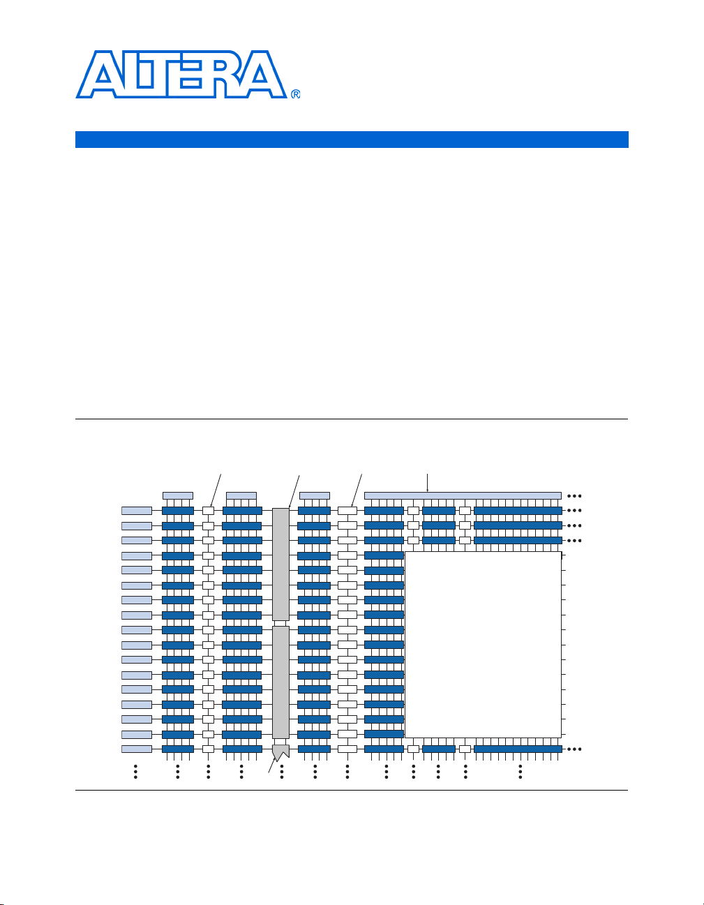
As shown in Figure 2–1, HardCopy Stratix devices preserve their Stratix
FPGA counterpart’s architecture, but the programmability for logic,
memory, and interconnect is removed. HardCopy Stratix devices are also
manufactured in the same process technology and process voltage as
Stratix FPGAs. Removing all configuration and programmable routing
resources and replacing it with direct metal interconnect results in
considerable die size reduction and the ensuing cost savings.
Figure 2–1. HardCopy Stratix Device Architecture
M512 RAM Blocks for
Dual-Port Memory, Shift
Registers, & FIFO Buffers
IOEs
IOEs
LABs
IOEs
LABs
IOEs
LABs
IOEs
LABs
IOEs
LABs
IOEs
LABs
IOEs
LABs
IOEs
LABs
IOEs
LABs
IOEs
LABs
IOEs
LABs
IOEs
LABs
IOEs
LABs
IOEs
LABs
IOEs
LABs
IOEs
LABs
IOEs
LABs
IOEs
LABs
LABs
LABs
LABs
LABs
LABs
LABs
LABs
LABs
LABs
LABs
LABs
LABs
LABs
LABs
LABs
LABs
DSP Blocks for
Multiplication and Full
Implementation of FIR Filters
DSP
Block
IOEs IOEs
LABs LABs
LABs
LABs LABs
LABs
LABs
LABs
LABs
LABs
LABs
LABs
LABs
LABs
LABs
LABs
LABs
LABs
LABs LABs
®
II des ign software, and, combined with a vast
®
IP for their high-volume applications.
M4K RAM Blocks
for True Dual-Port
Memory & Other Embedded
Memory Functions
IOEs Support DDR, PCI, GTL+, SSTL-3,
SSTL-2, HSTL, LVDS, LVPECL, PCML,
HyperTransport & other I/O Standards
LABs
LABs
LABs
LABs
LABs
LABs
LABs
LABs
LABs
LABs
LABs
LABs
LABs
LABs
LABs
LABs
LABs
LABs
LABs
LABs
LABs
LABs
LABs
LABs
M-RAM Block
Altera Corporation 2–1
September 2008
Page 20

HardCopy Stratix and Stratix FPGA Differences
The HardCopy Stratix family consists of base arrays that are common to
all designs for a particular device density. Design-specific customization
is done within the top two metal layers. The base arrays use an
area-efficient sea-of-logic-elements (SOLE) core an d extend the flexibility
of high-density Stratix FPGAs to a cost-effective, high-volume production
solution. With a seamless migration process employed in numerous
successful designs, functionality-verified Stratix FPGA designs can be
migrated to fixed-function HardCopy Stratix devices with minimal risk
and guaranteed first-time success.
The SRAM configuration cells of the original Stratix devices are replaced
in HardCopy Stratix devices by metal connects, which define the function
of each logic element (LE), digital signal processing (DSP) block,
phase-locked loop (PLL), embedded memory, and I/O cell in the device.
These resources are interconnected using metallization layers. Once a
HardCopy Stratix device has been manufactured, the functionality of the
dev ic e i s fixe d an d n o re -p ro gr am mi ng is po ss ib le . H ow ev er, as is th e c as e
with Stratix FPGAs, the PLLs can be dynamically configured in
HardCopy Stratix devices.
HardCopy Stratix
and Stratix FPGA
Differences
To ensure HardCopy Stratix device functionality and performance,
designers should thoroughly test the original Stratix FPGA-based design
for satisfactory results before committing the design for migration to a
HardCopy Stratix device. Unlike Stratix FPGAs, HardCopy Stratix
devices are customized at the time of manufacturing and therefore do not
have programmability support.
Since HardCopy Stratix devices are customized within the top two metal
layers, no configuration circuitry is required. Refer to “Power-Up Modes
in HardCopy Stratix Devices” on page 2–7 for more information.
Depending on the design, HardCopy Stratix devices can provide, on
average, a 50% performance improvement over equivalent Stratix
FPGAs. The performance improvement is achieved by die size reduction,
metal interconnect optimization, and customized signal buffering.
HardCopy Stratix devices consume, on average, 40% less power than
their equivalent Stratix FPGAs.
1 Designers can use the Quartus II software to design HardCopy
Stratix devices, estimate performance and power consumption,
and maximize system throughput.
2–2 Altera Corporation
September 2008
Page 21
Description, Architecture, and Features
Table 2–1 illustrates the differences between HardCopy Stratix and
Stratix devices.
Table 2–1. HardCopy Stratix and Stratix Device Comparison (Part 1 of 2)
HardCopy Stratix Stratix
Customized device. All
reprogrammability support is removed
and no configuration is required.
Average of 50% performance
improvement over corresponding
FPGA (1).
Average of 40% less power
consumption compared to
corresponding FPGA (1).
Contact Altera for information regarding
specific IP support.
Double data rate (DDR) SDRAM
maximum operating frequency is
pending characterization.
All routing connections are direct and
all unused routing is removed.
HC1S30 and HC1S40 devices have
two M-RAM blocks. HC1S80 devices
have six M-RAM blocks.
It is not possible to initialize M512 and
M4K RAM contents during power-up.
The contents of memory output
registers are unknown after power-on
reset (POR).
HC1S30 and HC1S40 devices have six
PLLs.
PLL dynamic reconfiguration uses
ROM for information. This
reconfiguration is performed in the
back-end and does not affect the
migration fl ow.
The I/O elements (IOEs) are equivalent
but not identical to FPGA IOEs due to
slight design optimizations for
HardCopy devices.
Re-programmable with configuration is
required upon power-up.
High-performance FPGA.
Standard FPGA power consumption.
IP support for all devices is available.
DDR SDRAM can operate at 200 MHz
for -5 speed grade devices.
MultiTrack™ routing stitches together
routing resources to provide a path.
EP1S30 and EP1S40 devices have four
M-RAM blocks. EP1S80 devices have
nine M-RAM blocks.
The contents of M512 and M4K RAM
blocks can be preloaded during
configuration with data specified in a
mem ory initia lization file (.m if).
The contents of memory output
registers are initialized to '0' after POR.
HC1S30 devices have 10 PLLs.
HC1S40 devices have 12 PLLs.
PLL dynamic reconfiguration uses a
MIF to initialize a RAM resource with
information.
The IOEs are optimized for the FPGA
architecture.
Altera Corporation 2–3
September 2008
Page 22
Logic Elements
Table 2–1. HardCopy Stratix and Stratix Device Comparison (Part 2 of 2)
HardCopy Stratix Stratix
The I/O drive strength for single-ended
I/O pins are slightly different and is
modeled in the HardCopy Stratix IBIS
models.
In the HC1S40 780-pin FineLine BGA®
device, the I/O pins U12 and U18 must
be connected to ground.
The BSDL file describes re-ordered
Joint Test Action Group (JTAG)
boundary-scan chains.
Note t o Table 2–1:
(1) Performance and power consumption are design dependant.
The I/O drive strength for single-ended
I/O pins are found in Stratix IBIS
models.
In the HC1S40 780-pin FineLine BGA
device, the I/O pins U12 and U18 are
available as general-purpose I/O pins.
The JTAG boundary-scan chain is
defined in the BSDL file.
Logic Elements
Embedded Memory
Logic is implemented in HardCopy Stratix devices using the same
architectural units as the Stratix device family. The basic unit is the logic
element (LE) with logic array blocks (LAB) consisting of 10 LEs. The
implementation of LEs and LABs is identical to the Stratix device family.
In the HardCopy Stratix device family, all extraneous routing resources
not essential to the specific design are removed for performance and die
size efficiency. Therefore, the MultiTrack interconnect for routing
implementation between LABs and other device resources in the Stratix
device family is no longer necessary in the HardCopy Stratix device
family.
Table 2–2 illustrates the differences between HardCopy Stratix and
Stratix logic.
Table 2–2. HardCopy Stratix and Stratix Logic Comparison
HardCopy Stratix Stratix
All routing connections are direct and
all unused routing is removed.
MultiTrack routing stitches routing
resources together to provide a path.
TriMatrix™ memory blocks from Stratix devices, including M512, M4K,
and M-RAM memory blocks, are available in HardCopy Stratix devices.
Embedded memory is seamlessly implemented in the equivalent
resource.
2–4 Altera Corporation
September 2008
Page 23

Description, Architecture, and Features
Although memory resource implementation is equivalent, the number of
specific M-RAM blocks are not necessarily the same between
corresponding Stratix and HardCopy Stratix devices. Table 2–3 shows the
number of M-RAM blocks available in each device.
Table 2–3. HardCopy Stratix and Stratix M-RAM Block Comparison
HardCopy Stratix Stratix
Device M-RAM Blocks Device M-RAM Blocks
HC1S25 2 EP1S25 2
HC1S30 2 EP1S30 4
HC1S40 2 EP1S40 4
HC1S60 6 EP1S60 6
HC1S830 6 EP1S830 9
In HardCopy Stratix devices, it is not possible to preload RAM contents
using a MIF after powering up; the output registers of memory blocks
will have unknown values. This occurs because there is no configuration
process that is executed.
1 Violating the setup or hold time requirements on address
registers could corrupt the memory contents. This requirement
applies to both read and write operations.
Table 2–4 illustrates the differences between HardCopy Stratix and
Stratix memory.
Table 2–4. HardCopy Stratix and Stratix Memory Comparison
HardCopy Stratix Stratix
HC1S30 and HC1S40 devices have
two M-RAM blocks. HC1S80 devices
have six M-RAM blocks.
It is not possible to initialize M512 and
M4k RAM contents during power-up.
The contents of memory output
registers are unknown after POR.
Altera Corporation 2–5
September 2008
EP1S30 and EP1S40 devices have four
M-RAM blocks. EP1S80 devices have
nine M-RAM blocks.
The contents of M512 and M4K RAM
blocks can be preloaded during
configuration with data specified in a
MIF.
The contents of memory output
registers are initialized to ‘0’ after POR.
Page 24
DSP Blocks
DSP Blocks
PLLs and Clock Networks
DSP blocks in HardCopy Stratix devices are architecturally identical to
those in Stratix devices. The number of DSP blocks available in
HardCopy Stratix devices matches the number of DSP blocks available in
the corresponding Stratix device.
The PLLs in HardCopy Stratix devices are identical to those in Stratix
devices. The clock networks are also implemented exactly as they are in
Stratix devices. The number of PLLs can vary between corresponding
Stratix and HardCopy Stratix devices. Ta b l e 2 –5 shows the number of
PLLs available in each device.
Table 2–5. HardCopy Stratix and Stratix PLL Comparison
HardCopy Stratix Stratix
Device PLLs Device PLLs
HC1S25 6 EP1S25 6
HC1S30 6 EP1S30 10
HC1S40 6 EP1S40 12
HC1S60 12 EP1S60 12
EP1S830 12 EP1S830 12
Table 2–6 illustrates the differences between HardCopy Stratix and
Stratix PLLs.
Table 2–6. HardCopy Stratix and Stratix PLL Differences
HardCopy Stratix Stratix
HC1S30 and HC1S40 devices have six
PLLs.
PLL dynamic reconfiguration uses
ROM for information. This
reconfiguration is performed in the
back-end and does not affect the
migration fl ow.
I/O Structure and Features
2–6 Altera Corporation
The HardCopy Stratix IOEs are equivalent, but not identical to, the Stratix
FPGA IOEs. This is due to the reduced die size, layout difference, and
metal customization of the HardCopy Stratix device. The differences are
minor but may be relevant to customers designing with tight DC and
switching characteristics. However, no signal integrity concerns are
introduced with HardCopy Stratix IOEs.
HC1S30 devices have 10 PLLs.
HC1S40 devices have12 PLLs.
PLL dynamic reconfiguration uses a
MIF to initialize a RAM resource with
information.
September 2008
Page 25
Description, Architecture, and Features
When designing with very tight timing constraints (for example, DDR or
quad data rate [QDR]), or if using the programmable drive strength
option, Altera recommends verifying final drive strength using updated
IBIS models located on the Altera website at www.alter a.com.
Differential I/O standards are unaffected.
I/O pin placement and VREF pin placement rules are identical between
HardCopy Strati x and Stratix devices. Unused pin settings will carry o ver
from Stratix device settings and are implemented as tri-stated outputs
driving ground or outputs driving V
CC
.
In Stratix EP1S40 780-pin FineLine BGA FPGAs, the I/O pins U12 and
U18 are available as general-purpose I/O pins. In the FPGA prototype,
EP1S40F780_HARDCOPY_FPGA_PROTOTYPE, and in the Hardcopy
Stratix HC1S40 780-pin FineLine BGA device, the I/O pins U12 and U18
must be connected to ground. HC1S40 780-pin FineLine BGA and
EP1S40F780_HARDCOPY_FPGA_PROTOTYPE pin-outs are identical.
Table 2–7 illustrates the differences between HardCopy Stratix and
Stratix I/O pins.
Table 2–7. HardCopy Stratix and Stratix I/O Pin Comparison
HardCopy Stratix Stratix
Power-Up Modes in HardCopy Stratix Devices
The IOEs are equivalent, but not
identical to, the FPGA IOEs due to
slight design optimizations for
HardCopy devices.
The I/O drive strength for single-ended
I/O pins are slightly different and are
found in the HardCopy Stratix IBIS
models.
In the HC1S40 780-pin FineLine BGA
device, the I/O pins U12 and U18 must
be connected to ground.
Designers do not need to configure HardCopy Stratix devices, unlike
their FPGA counterparts. However, to facilitate seamless migration,
configuration can be emulated in HardCopy Stratix devices.
The modes in which a HardCopy Stratix device can be made ready for
operation after power-up are: instant on, instant on after 50 ms, and
IOEs are optimized for the FPGA
architecture.
The I/O drive strength for single-ended
I/O pins are found in Stratix IBIS
models.
In the EP1S40 780-pin FineLine BGA
device, the I/O pins U12 and U18 are
available as general-purpose I/O pins.
configuration emulation. These modes are briefly described below.
Altera Corporation 2–7
September 2008
Page 26

Hot Socketing
■ In instant on mode, the HardCopy Stratix device is available for use
shortly after the device receives power. The on-chip POR circuit
resets all registers. The CONF_DONE output is tri-stated once the POR
has elapsed. No configuration device or configuration data is
necessary.
■ In instant on after 50 ms mode, the HardCopy Stratix device
performs in a fashion similar to the instant on mode, except that there
is an additional delay of 50 ms, during which time the device is held
in reset stage. The CONF_DONE output is pulled low during this time,
and then tri-stated after the 50 ms have elapsed. No configuration
device or configuration data is necessary for this option.
■ In configuration emulation mode, the HardCopy series device
emulates the behavi or of an APEX or Stratix FPGA during its
configuration phase. When this mode is used, the HardCopy device
uses a configuration emulation circuit to receive configuration bit
streams. When all the configuration data is received, the HardCopy
series device transitions into an initialization phase and releases the
CONF_DONE pin to be pulled high. Pulling the CONF_DONE pin high
signals that the HardCopy series device is ready for normal
operation. If the optional open-drain INIT_DONE output is used, the
normal operation is delayed until this signal is released by the
HardCopy series device.
1 HardCopy II and some HardCopy Stratix devices do not
support configuration emulation mode.
Instant on and instant on after 50 ms modes are the recommended
power-up modes because these modes are similar to an ASIC’s
functionality upon power-up. No changes to th e existing board design or
the configuration software are required.
All three modes provide significant benefits to system designers. They
enable seamless migration of the design from the FPGA device to the
HardCopy device with no changes to the existing board design or the
configuration software. The pull-up resistors on nCONFIG, nSTATUS, and
CONF_DONE should be left on the printed circuit board.
f For more information, refer to the HardCopy Series Configuration
Emulation chapter in the HardCopy Series Handbook.
Hot Socketing
2–8 Altera Corporation
HardCopy Stratix devices support hot socketing without any external
components. In a hot socketing situation, a device’s output buffers are
turned off during system power up or power down. To simplify board
design, HardCopy Stratix devices support any power-up or power-down
sequence (V
CCIO
and V
). For mixed-voltage environments, you can
CCINT
September 2008
Page 27

Description, Architecture, and Features
drive signals into the device before or during power up or power down
without damaging the device. HardCopy Stratix devices do not drive out
until they have attained proper operating conditions.
HARDCOPY_ FPGA_ PROTOTYPE Devices
You can power up or power down the V
CCIO
and V
CCINT
pi ns in any
sequence. The power supply ramp rates can range from 100 ns to 100 ms.
During hot socketing, the I/O pin capacitance is less than 15 pF and the
clock pin capacitance is less than 20 pF.
■ The hot socketing DC specification is | I
■ The hot socketing AC specification is | I
| < 300 µA.
IOPIN
| < 8 mA for 10 ns or
IOPIN
less. This specification takes into account the pin capacitance only.
Additional capacitance for trace, connector, and loading needs to be
taken into consideration separately. I
is the current at any user
IOPIN
I/O pin on the device.
1 The DC specifi cation applies when all V
supplies to the device
CC
are stable in the powered-up or powered-down conditions. For
the AC specification, the peak current duration due to power-up
transients is 10 ns or less.
HARDCOPY_FPGA_PROTOTYPE devices are Stratix FPGAs available
for designers to prototype their HardCopy Stratix designs and perform
in-system verification before migration to a HardCopy Stratix device. The
HARDCOPY_FPGA_PROTOTYPE devices have the same available
resources as in the final HardCopy Stratix devices.
The Quartus II software version 4.1 and later contains the latest timing
models. For designs with tight timing constraints, Altera strongly
recommends compiling the design with the Quartus II software
version 4.1 or later. To properly verify I/O features, it is important to
design with the HARDCOPY_FPGA_PROTOTYPE device option prior to
migrating to a HardCopy Stratix device.
Altera Corporation 2–9
September 2008
Page 28
Document Revision History
1 Some HARDCOPY_FPGA_PROTOTYPE devices, as indicated
in Table 2–8, have fewer M-RAM blocks compared to the
equivalent Stratix FPGAs. The selective removal of these
resources provides a significant price benefit to designers using
HardCopy Stratix devices.
Table 2–8. M-RAM Block Comparison Between Various Devices
Number
HARDCOPY_FPGA_PROTOTYPE
Devices
HardCopy Stratix Devices Stratix Devices
of LEs
Device M-RAM Blocks Device M-RAM Blocks Device M-RAM Blocks
25,660 EP1S25 2 HC1S25 2 EP1S25 2
32,470 EP1S30 2 HC1S30 2 EP1S30 4
41,250 EP1S40 2 HC1S40 2 EP1S40 4
57,120 EP1S60 6 HC1S60 6 EP1S60 6
79,040 EP1S830 6 HC1S830 6 EP1S830 9
f For more information about how the various features in the Quartus II
software can be used for designing HardCopy Stratix devices, refer to
the Quartus II Support for HardCopy Stratix Devices chapter of the
HardCopy Series Handbook.
HARDCOPY_FPGA_PROTOTYPE FPGA devices have the identical
speed grade as the equivalent Stratix FPGAs. However, HardCopy Stratix
devices are customized and do not have any speed grading. HardCopy
Stratix devices, on an average, can be 50% faster than their equivalent
HARDCOPY_FPGA_PROTOTYPE devices. The actual improvement is
design-dependent.
Document
Table 2–9 shows the revision history for this chapter.
Revision History
Table 2–9. Document Revision History (Part 1 of 2)
Date and Document
Version
September 2008
v3.4
June 2007 v3.3 ● Updated Table 2–1.
2–10 Altera Corporation
Revised chapter number and metadata. —
● Added note to the “Embedded Memory” section.
● Updated the “Hot Socketing” section.
Changes Made Summary of Changes
—
September 2008
Page 29
Table 2–9. Document Revision History (Part 2 of 2)
Description, Architecture, and Features
Date and Document
Version
December 2006
Updated revision history. —
Changes Made Summary of Changes
v3.2
March 2006 Formerly chapter 6; no content change. —
October 2005 v3.1 ● Minor edits
● Updated graphics
May 2005
v3.0
January 2005
v2.0
● Added Table 6-1
● Added the Logic Elements section
● Added the Embedded Memory section
● Added the DSP Blocks section
● Added the PLLs and Clock Networks section
● Added the I/O Structure and Features section
● Added summary of I/O and timing differences between
Stratix FPGAs and HardCopy Stratix devices
● Removed section on Quartus II support of HardCopy
Minor edits.
Minor update.
Minor update.
Stratix devices
● Added “Hot Socketing” section
August 2003
Edited section headings’ hierarchy. Minor edits.
v1.1
June 2003
v1.0
Initial release of Chapter 6, Description, Architecture and
Features, in the HardCopy Device Handbook
—
Altera Corporation 2–11
September 2008
Page 30

Document Revision History
2–12 Altera Corporation
September 2008
Page 31

H51004-3.4
3. Boundary-Scan Support
IEEE Std. 1149.1 (JTAG) Boundary-Scan Support
Table 3–1. HardCopy Stratix JTAG Instructions (Part 1 of 2)
JTAG Instruction Instruction Code Description
SAMPLE/PRELOAD 00 0000 0101
EXTEST (1) 00 0000 0000
BYPASS 11 1111 1111 Places the 1-bit bypass register between the TDI and TDO pins,
USERCODE 00 0000 0111 Selects the 32-bit USERCODE register and places it between the
IDCODE 00 0000 0110 Selects the IDCODE register and places it between TDI and TDO,
HIGHZ (1) 00 0000 1011 Places the 1-bit bypass register between the TDI and TDO pins,
All HardCopy® Stratix® structured ASICs provide JTAG boundry-scan
test (BST) circuitry that complies with the IEEE Std. 1149.1-1990
specification. The BST architecture offers the capability to efficiently test
components on printed circuit boards (PCBs) with tight lead spacing by
testing pin connections, without using physical test probes, and
capturing functional data while a device is in normal operation.
Boundary-scan cells in a device can force signals onto pins, or capture
data from pin or core logic signals. Forced test data is serially shifted into
the boundary-scan cells. Captured data is serially shifted out and
externally compared to expected results.
A device using the JTAG interface uses four required pins, TDI, TDO, TMS,
and TCK, and one optional pin, TRST. HardCopy Stratix devices support
the JTAG instructions as shown in Table 3–1.
Allows a snapshot of signals at the device pins to be captured and
examined during normal device operation, and permits an initial
data pattern to be output at the device pins.
Allows the external circuitry and board-level interconnects to be
tested by forcing a test pattern at the output pins and capturing test
results at the input pins.
which allows the BST data to pass synchronously through selected
devices to adjacent devices during normal device operation.
TDI and TDO pins, allowing the USERCODE to be serially shifted
out of TDO.
allowing the IDCODE to be serially shifted out of TDO.
which allows the BST data to pass synchronously through selected
devices to adjacent devices during normal device operation, while
tri-stating all of the I/O pins.
Altera Corporation 3–1
September 2008 Preliminary
Page 32

HardCopy Series Handbook, Volume 1
Table 3–1. HardCopy Stratix JTAG Instructions (Part 2 of 2)
JTAG Instruction Instruction Code Description
CLAMP (1) 00 0000 1010 Places the 1-bit bypass register between the TDI and TDO pins,
which allows the BST data to pass synchronously through selected
devices to adjacent devices during normal device operation while
holding I/O pins to a state defined by the data in the boundary-scan
register.
Note t o Table 3–1:
(1) Bus hold and weak pull-up resistor features override the high-impedance state of HIGHZ, CLAMP, and EXTEST.
f The boundary-scan description language (BSDL) files for HardCopy
Stratix devices are different from the corresponding Stratix FPGAs. The
BSDL files for HardCopy Stratix devices are available for download
from the Altera website at www.altera.com.
The HardCopy Stratix device instruction register length is 10 bits; the
USERCODE register length is 32 bits. The USERCODE registers are
mask-programmed, so they are not re-programmable. The designer can
choose an appropriate 32-bit sequence to program into the USERCODE
registers.
Tables 3–2 and 3–3 show the boundary-scan register length and device
IDCODE information for HardCopy Stratix devices.
Table 3–2. HardCopy Stratix Boundary-Scan Register Length
Device Maximum Boundary-Scan Register Length
HC1S25 672-pin FineLine BGA 1,458
HC1S30 780-pin FineLine BGA 1,878
HC1S40 780-pin FineLine BGA 1,878
HC1S60 1,020-pin FineLine BGA 2,382
HC1S80 1,020-pin FineLine BGA 2,382
3–2 Altera Corporation
Preliminary September 2008
Page 33

IEEE Std. 1149.1 (JTAG) Boundary-Scan Support
Table 3–3. 32-Bit HardCopy Stratix Device IDCODE
IDCODE (32 Bits) (1)
Device
HC1S25 0000 0010 0000 0000 0011 000 0110 1110 1
HC1S30 0000 0010 0000 0000 0100 000 0110 1110 1
HC1S40 0000 0010 0000 0000 0101 000 0110 1110 1
HC1S60 0000 0010 0000 0000 0110 000 0110 1110 1
HC1S80 0000 0010 0000 0000 0111 000 0110 1110 1
Notes to Tab l e 3 –3 :
(1) The most significant bit (MSB) is on the left.
(2) The IDCODE’s least significant bit (LSB) is always 1.
Version
(4 Bits)
Part Number
(16 Bits)
Manufacturer Identity
(11 Bits)
(1 Bit) (2)
Figure 3–1 shows the timing requirements for the JTAG signals.
Figure 3–1. HardCopy Stratix JTAG Waveforms
TMS
LSB
TDI
t
JCP
t
JCH
t
JCL
t
JPSU
t
JPH
TCK
t
JPZX
t
JPCO
t
JPXZ
TDO
t
JSH
t
JSCO
t
JSXZ
Signal
to Be
Captured
Signal
to Be
Driven
t
JSZX
t
JSSU
Altera Corporation 3–3
September 2008 Preliminary
Page 34

HardCopy Series Handbook, Volume 1
Table 3–4 shows the JTAG timing parameters and values for HardCopy
Stratix devices.
Table 3–4. HardCopy Stratix JTAG Timing Parameters and Values
Symbol Parameter Min Max Unit
t
JCP
t
JCH
t
JCL
t
JPSU
t
JPH
t
JPCO
t
JPZX
t
JPXZ
t
JSSU
t
JSH
t
JSCO
t
JSZX
t
JSXZ
TCK clock period 100 ns
TCK clock high time
TCK clock low time
50 ns
50 ns
JTAG port setup time 20 ns
JTAG port hold time 45 ns
JTAG port clock to output 25 ns
JTAG port high impedance to valid output 25 ns
JTAG port valid output to high impedance 25 ns
Capture register setup time 20 ns
Capture register hold time 45 ns
Update register clock to output 35 ns
Update register high impedance to valid output 35 ns
Update register valid output to high impedance 35 ns
f For more information on JTAG, refer to AN 39: IEEE Std. 1149.1 (JTAG)
Boundary-Scan Testing in Altera Devices.
Document
Table 3–5 shows the revision history for this chapter.
Revision History
Table 3–5. Document Revision History (Part 1 of 2)
Date and Document
Version
September 2008
v3.4
June 2007 v3.3 Updated Figure 3–1.—
December 2006
v3.2
March 2006 Formerly chapter 7; no content change. —
3–4 Altera Corporation
Preliminary September 2008
Updated chapter number and metadata. —
Updated revision history. —
Changes Made Summary of Changes
Page 35

Table 3–5. Document Revision History (Part 2 of 2)
Document Revision History
Date and Document
Version
October 2005 v3.1 ● Minor edits
● Graphic updates
May 2005
v3.0
January 2005
v2.0
June 2003
v1.0
Updated “IEEE Std. 1149.1 (JTAG) Boundary-Scan
Support” section
Added information about USERCODE registers
Initial release of Chapter 7, Boundary-Scan Support, in the
HardCopy Device Handbook
Changes Made Summary of Changes
—
Altera Corporation 3–5
September 2008 Preliminary
Page 36

HardCopy Series Handbook, Volume 1
3–6 Altera Corporation
Preliminary September 2008
Page 37

H51005-3.4
4. Operating Conditions
Recommended
Operating
Tables 4–1 through 4–3 provide information on absolute maximum
ratings, recommended operating conditions, DC operating conditions,
and capacitance for 1.5-V HardCopy
®
Stratix® devices.
Conditions
Table 4–1. HardCopy Stratix Device Absolute Maximum Ratings Notes (1), (2)
Symbol Parameter Conditions Minimum Maximum Unit
V
CCINT
V
CCIO
V
I
I
OUT
T
STG
T
J
Table 4–2. HardCopy Stratix Device Recommended Operating Conditions
Symbol Parameter Conditions Minimum Maximum Unit
V
CCINT
V
CCIO
V
I
V
O
T
J
Supply voltage With respect to ground –0.5 2.4 V
–0.5 4.6 V
DC input voltage (3) –0.5 4.6 V
DC output current, per pin –25 40 mA
Storage temperature No bias –65 150 °C
Junction temperature BGA packages under bias 135 °C
Supply voltage for internal logic
and input buffers
Supply voltage for output
buffers, 3.3-V operation
Supply voltage for output
buffers, 2.5-V operation
Supply voltage for output
buffers, 1.8-V operation
Supply voltage for output
buffers, 1.5-V operation
Input voltage (3), (6) –0.5 4.1 V
Output voltage 0 V
Operating junction temperature For commercial use 0 85 °C
(4) 1.425 1.575 V
(4), (5) 3.00 (3.135) 3.60 (3.465) V
(4) 2.375 2.625 V
(4) 1.71 1.89 V
(4) 1.4 1.6 V
CCIO
For industrial use –40 100 °C
V
Altera Corporation 4–1
September 2008
Page 38

Recommended Operating Conditions
Table 4–3. HardCopy Stratix Device DC Operating Conditions Note (7)
Symbol Parameter Conditions Minimum Typical Maximum Unit
I
I
I
OZ
I
CC0
R
CONF
Notes to Tables 4–1 through 4–3:
(1) Refer to the Operating Requirements for Altera Devices Data Sheet.
(2) Conditions beyond those listed in Ta b l e 4 – 1 may cause permanent damage to a device. Additionally, device
(3) M inim um DC inp ut is –0. 5 V. Duri ng tran siti ons, the i nputs may und ersh oot t o –2 V or ov ersh oot to 4 .6 V f or input
(4) Maximum V
(5) V
(6) All pins, including dedicated inputs , clock, I/O, and JTAG pins, may be driven before V
(7) Typical values are for TA = 25 °C, V
(8) This value is specified for normal device operation. The value may vary during power up. This applies for all V
(9) Pin pull-up resistance values will be lower if an external source drives the pin hig her than V
Input pin leakage current VI = V
Tri-stated I/O pin leakage
current
VCC supply current
(standby) (All memory
VO = V
(8)
VI = ground, no load,
no toggling inputs
to 0 V (8) –10 10 μA
CCIOmax
CCIOmax
to 0 V
–10 10 μA
mA
blocks in power-down
mode)
Value of I/O pin pull-up
resistor before and
during configuration
Recommended value of
Vi=0; V
Vi=0; V
Vi=0; V
Vi=0; V
= 3.3 V (9) 15 25 50 kΩ
CCIO
= 2.5 V (9) 20 45 70 kΩ
CCIO
= 1.8 V (9) 30 65 100 kΩ
CCIO
= 1.5 V (9) 50 100 150 kΩ
CCIO
12kΩ
I/O pin external
pull-down resistor before
and during configuration
operation at the absolute maximum ratings for extended periods of time may have adverse affects on the device.
currents less than 100 mA and periods shorter than 20 ns.
rise time is 100 ms, and VCC must r ise m onotonically.
CC
maximum a nd minimum conditions for LVPECL, LVDS, and 3.3-V PCML are shown in parentheses.
CCIO
CCIN T
and V
CCIO
are
powered.
= 1.5 V, and V
CCIN T
= 1.5 V, 1.8 V, 2.5 V, and 3.3 V.
CCIO
CCIO
settings (3.3, 2.5, 1.8, and 1.5 V).
.
CCIO
4–2 Altera Corporation
September 2008
Page 39

Operating Conditions
Tables 4–4 through 4–31 list the DC operating specifications for the
supported I/O standards. These tables list minimal specifications only;
HardCopy Stratix devices may exceed these specifications. Table 4–32
provides information on capacitance for 1.5-V HardCopy Stratix
devices.
Table 4–4. LVTTL Specifications
Symbol Parameter Conditions Minimum Maximum Unit
V
V
V
V
V
CCIO
IH
IL
OH
OL
Output supply voltage 3.0 3.6 V
High-level input voltage 1.7 4.1 V
Low-level input voltage –0.5 0.7 V
High-level output voltage IOH = –4 to –24 mA (1) 2. 4 V
Low-level output voltage IOL = 4 to 24 mA (1) 0.45 V
Table 4–5. LVCMOS Specifications
Symbol Parameter Conditions Minimum Maximum Unit
V
V
V
V
V
CCIO
IH
IL
OH
OL
Output supply voltage 3.0 3.6 V
High-level input voltage 1.7 4.1 V
Low-level input voltage –0.5 0.7 V
High-level output voltage V
CCIO
= 3.0,
V
– 0.2 V
CCIO
IOH = –0.1 mA
Low-level output voltage V
CCIO
= 3.0,
0.2 V
IOL = 0.1 mA
Table 4–6. 2.5-V I/O Specifications
Symbol Parameter Conditions Minimum Maximum Unit
V
CCIO
V
IH
V
IL
V
OH
V
OL
Altera Corporation 4–3
September 2008
Output supply voltage 2.375 2.625 V
High-level input voltage 1.7 4.1 V
Low-level input voltage –0.5 0.7 V
High-level output voltage IOH = –0.1 mA 2.1 V
IOH = –1 mA 2.0 V
IOH = –2 to –16 mA (1) 1. 7 V
Low-level output voltage IOL = 0.1 mA 0.2 V
IOL = 1 mA 0.4 V
IOL = 2 to 16 mA (1) 0.7 V
Page 40

Recommended Operating Conditions
Table 4–7. 1.8-V I/O Specifications
Symbol Parameter Conditions Minimum Maximum Unit
V
V
V
V
V
CCIO
IH
IL
OH
OL
Output supply voltage 1.65 1.95 V
High-level input voltage 0.65 × V
CCIO
Low-level input voltage –0.3 0.35 × V
High-level output voltage IOH = –2 to –8 mA (1) V
– 0.45 V
CCIO
2.25 V
CCIO
Low-level output voltage IOL = 2 to 8 mA (1) 0.45 V
Table 4–8. 1.5-V I/O Specifications
Symbol Parameter Conditions Minimum Maximum Unit
V
V
V
V
V
CCIO
IH
IL
OH
OL
Output supply voltage 1.4 1.6 V
High-level input voltage 0.65 × V
CCIOVCCIO
Low-level input voltage –0.3 0.35 × V
High-level output voltage IOH = –2 mA (1) 0.75 × V
CCIO
Low-level output voltage IOL = 2 mA (1) 0.25 × V
+ 0.3 V
CCIO
CCIO
V
V
V
V
Table 4–9. 3.3-V LVDS I/O Specifications (Part 1 of 2)
Symbol Parameter Conditions Minimum Typical Maximum Unit
V
CCIO
V
ID
4–4 Altera Corporation
I/O supply voltage 3.135 3.3 3.465 V
Input differential voltage
swing
0.1 V < VCM < 1.1 V
J = 1 through 10
1.1 V ≤ VCM ≤ 1.6 V
300 1,000 mV
200 1,000 mV
J = 1
1.1 V ≤ VCM ≤ 1.6 V
100 1,000 mV
J = 2 through10
1.6 V < VCM < 1.8 V
300 1,000 mV
J = 1 through 10
September 2008
Page 41

Operating Conditions
Table 4–9. 3.3-V LVDS I/O Specifications (Part 2 of 2)
Symbol Parameter Conditions Minimum Typical Maximum Unit
V
V
Δ V
V
Δ V
R
ICM
OD
OCM
L
Input common mode
voltage
(2) Output differential
voltage
Change in VOD between
OD
high and low
Output common mode
voltage
Change in V
OCM
OCM
high and low
Receiver differential
input resistor
between
LV DS
100 1,100 mV
0.3 V < VID < 1.0 V
J = 1 through 10
LV DS
1,600 1,800 mV
0.3 V < VID < 1.0 V
J = 1 through 10
LV DS
1,100 1,600 mV
0.2 V < VID < 1.0 V
J = 1
LV DS
1,100 1,600 mV
0.1 V < VID < 1.0 V
J = 2 through 10
RL = 100 Ω 250 375 550 mV
RL = 100 Ω 50 mV
RL = 100 Ω 1,125 1,200 1,375 mV
RL = 100 Ω 50 mV
90 100 110 Ω
Altera Corporation 4–5
September 2008
Page 42

Recommended Operating Conditions
Table 4–10. 3.3-V PCML Specifications
Symbol Parameter Conditions Minimum Typical Maximum Unit
V
CCIO
V
ID
V
ICM
VOD Output differential
Δ V
V
OCM
Δ V
V
T
R
1
R
2
I/O supply voltage 3.135 3.3 3.465 V
Input differential voltage
300 600 mV
swing
Input common mode
1.5 3.465 V
voltage
300 370 500 mV
voltage
Change in VOD between
OD
high and low
Output common mode
2.5 2.85 3.3 V
voltage
OCM
Change in V
OCM
between
high and low
Output termination
V
CCIO
voltage
Output external pull-up
45 50 55 Ω
resistors
Output external pull-up
45 50 55 Ω
resistors
50 mV
50 mV
V
Table 4–11. LVPECL Specifications
Symbol Parameter Conditions Minimum Typical Maximum Unit
V
CCIO
V
ID
V
ICM
VOD Output differential
V
OCM
R
L
4–6 Altera Corporation
I/O supply voltage 3.135 3.3 3.465 V
Input differential voltage
300 1,000 mV
swing
Input common mode
12V
voltage
RL = 100 Ω 525 700 970 mV
voltage
Output common mode
RL = 100 Ω 1.5 1.7 1.9 V
voltage
Receiver differential
90 100 110 Ω
input resistor
September 2008
Page 43

Operating Conditions
Table 4–12. HyperTransport Technology Specifications
Symbol Parameter Conditions Minimum Typical Maximum Unit
V
CCIO
V
ID
V
ICM
VOD Output differential
Δ V
V
OCM
Δ V
R
L
I/O supply voltage 2.375 2.5 2.625 V
Input differential voltage
300 900 mV
swing
Input common mode
300 900 mV
voltage
RL = 100 Ω 380 485 820 mV
voltage
Change in VOD between
OD
RL = 100 Ω 50 mV
high and low
Output common mode
RL = 100 Ω 440 650 780 mV
voltage
OCM
Change in V
OCM
between
RL = 100 Ω 50 mV
high and low
Receiver differential
90 100 110 Ω
input resistor
Table 4–13. 3.3-V PCI Specifications
Symbol Parameter Conditions Minimum Typical Maximum Unit
V
V
V
V
V
CCIO
IH
IL
OH
OL
Output supply voltage 3.0 3.3 3.6 V
High-level input voltage 0.5 × V
CCIO
Low-level input voltage –0.5 0.3 × V
High-level output voltage I
Low-level output voltage I
= –500 μA0.9 × V
OUT
= 1,500 μA0.1 × V
OUT
CCIO
V
CCIO
+ 0.5 V
CCIO
CCIO
V
V
V
Table 4–14. PCI-X 1.0 Specifications
Symbol Parameter Conditions Minimum Typical Maximum Unit
V
CCIO
V
IH
V
IL
V
IPU
V
OH
V
OL
Altera Corporation 4–7
September 2008
Output supply voltage 3.0 3.6 V
High-level input voltage 0.5 × V
CCIO
Low-level input voltage –0.5 0.35 × V
Input pull-up voltage 0.7 × V
High-level output voltage I
Low-level output voltage I
= –500 μA0.9 × V
OUT
= 1,500 μA0.1 × V
OUT
CCIO
CCIO
V
CCIO
+ 0.5 V
CCIO
CCIO
V
V
V
V
Page 44

Recommended Operating Conditions
Table 4–15. GTL+ I/O Specifications
Symbol Parameter Conditions Minimum Typical Maximum Unit
V
TT
V
REF
V
IH
V
IL
V
OL
Termination voltage 1.35 1.5 1.65 V
Reference voltage 0.88 1.0 1.12 V
High-level input voltage V
Low-level input voltage V
+ 0.1 V
REF
– 0.1 V
REF
Low-level output voltage IOL = 34 mA (1) 0.65 V
Table 4–16. GTL I/O Specifications
Symbol Parameter Conditions Minimum Typical Maximum Unit
V
TT
V
REF
V
IH
V
IL
V
OL
Termination voltage 1.14 1.2 1.26 V
Reference voltage 0.74 0.8 0.86 V
High-level input voltage V
Low-level input voltage V
+ 0.05 V
REF
– 0.05 V
REF
Low-level output voltage IOL = 40 mA (1) 0.4 V
Table 4–17. SSTL-18 Class I Specifications
Symbol Parameter Conditions Minimum Typical Maximum Unit
V
CCIO
V
REF
V
TT
V
IH(DC)
V
IL(DC)
V
IH(AC)
V
IL(AC)
V
OH
V
OL
4–8 Altera Corporation
Output supply voltage 1.65 1.8 1.95 V
Reference voltage 0.8 0.9 1.0 V
Termination voltage V
High-level DC input
– 0.04 V
REF
V
+ 0.125 V
REF
REF
V
+ 0.04 V
REF
voltage
Low-level DC input
V
– 0.125 V
REF
voltage
High-level AC input
V
+ 0.275 V
REF
voltage
Low-level AC input
V
– 0.275 V
REF
voltage
High-level output voltage IOH = –6.7 mA (1) VTT + 0.475 V
Low-level output voltage IOL = 6.7 mA (1) VTT – 0.475 V
September 2008
Page 45

Operating Conditions
Table 4–18. SSTL-18 Class II Specifications
Symbol Parameter Conditions Minimum Typical Maximum Unit
V
V
V
V
V
V
V
V
V
CCIO
REF
TT
IH(DC)
IL(DC)
IH(AC)
IL(AC)
OH
OL
Output supply voltage 1.65 1.8 1.95 V
Reference voltage 0.8 0.9 1.0 V
Termination voltage V
High-level DC input
– 0.04 V
REF
V
+ 0.125 V
REF
REF
V
+ 0.04 V
REF
voltage
Low-level DC input
V
– 0.125 V
REF
voltage
High-level AC input
V
+ 0.275 V
REF
voltage
Low-level AC input
V
– 0.275 V
REF
voltage
High-level output voltage IOH = –13.4 mA (1) VTT + 0.630 V
Low-level output voltage IOL = 13.4 mA (1) VTT – 0.630 V
Table 4–19. SSTL-2 Class I Specifications
Symbol Parameter Conditions Minimum Typical Maximum Unit
V
V
V
V
V
V
V
V
V
CCIO
TT
REF
IH(DC)
IL(DC)
IH(AC)
IL(AC)
OH
OL
Output supply voltage 2.375 2.5 2.625 V
Termination voltage V
– 0.04 V
REF
REF
V
+ 0.04 V
REF
Reference voltage 1.15 1.25 1.35 V
High-level DC input
V
+ 0.18 3.0 V
REF
voltage
Low-level DC input
–0.3 V
– 0.18 V
REF
voltage
High-level AC input
V
+ 0.35 V
REF
voltage
Low-level AC input
V
– 0.35 V
REF
voltage
High-level output voltage IOH = –8.1 mA (1) VTT + 0.57 V
Low-level output voltage IOL = 8.1 mA (1) VTT – 0.57 V
Table 4–20. SSTL-2 Class II Specifications (Part 1 of 2)
Symbol Parameter Conditions Minimum Typical Maximum Unit
V
CCIO
V
TT
Altera Corporation 4–9
September 2008
Output supply voltage 2.375 2.5 2.625 V
Termination voltage V
– 0.04 V
REF
REF
V
+ 0.04 V
REF
Page 46

Recommended Operating Conditions
Table 4–20. SSTL-2 Class II Specifications (Part 2 of 2)
Symbol Parameter Conditions Minimum Typical Maximum Unit
V
V
V
V
V
V
V
REF
IH(DC)
IL(DC)
IH(AC)
IL(AC)
OH
OL
Reference voltage 1.15 1.25 1.35 V
High-level DC input
V
+ 0.18 V
REF
+ 0.3 V
CCIO
voltage
Low-level DC input
–0.3 V
– 0.18 V
REF
voltage
High-level AC input
V
+ 0.35 V
REF
voltage
Low-level AC input
V
– 0.35 V
REF
voltage
High-level output voltage IOH = –16.4 mA (1) VTT + 0.76 V
Low-level output voltage IOL = 16.4 mA (1) VTT – 0.76 V
Table 4–21. SSTL-3 Class I Specifications
Symbol Parameter Conditions Minimum Typical Maximum Unit
V
V
V
V
V
V
V
V
V
CCIO
TT
REF
IH(DC)
IL(DC)
IH(AC)
IL(AC)
OH
OL
Output supply voltage 3.0 3.3 3.6 V
Termination voltage V
– 0.05 V
REF
REF
V
+ 0.05 V
REF
Reference voltage 1.3 1.5 1.7 V
High-level DC input
V
+ 0.2 V
REF
+ 0.3 V
CCIO
voltage
Low-level DC input
–0.3 V
– 0.2 V
REF
voltage
High-level AC input
V
+ 0.4 V
REF
voltage
Low-level AC input
V
REF
– 0.4 V
voltage
High-level output voltage IOH = –8 mA (1) VTT + 0.6 V
Low-level output voltage IOL = 8 mA (1) VTT – 0.6 V
Table 4–22. SSTL-3 Class II Specifications (Part 1 of 2)
Symbol Parameter Conditions Minimum Typical Maximum Unit
V
CCIO
V
TT
V
REF
4–10 Altera Corporation
Output supply voltage 3.0 3.3 3.6 V
Termination voltage V
– 0.05 V
REF
REF
V
+ 0.05 V
REF
Reference voltage 1.3 1.5 1.7 V
September 2008
Page 47

Operating Conditions
Table 4–22. SSTL-3 Class II Specifications (Part 2 of 2)
Symbol Parameter Conditions Minimum Typical Maximum Unit
V
V
V
V
V
V
IH(DC)
IL(DC)
IH(AC)
IL(AC)
OH
OL
High-level DC input
V
+ 0.2 V
REF
+ 0.3 V
CCIO
voltage
Low-level DC input
–0.3 V
– 0.2 V
REF
voltage
High-level AC input
V
+ 0.4 V
REF
voltage
Low-level AC input
V
REF
– 0.4 V
voltage
High-level output voltage IOH = –16 mA (1) VTT + 0.8 V
Low-level output voltage IOL = 16 mA (1) VTT – 0.8 V
Table 4–23. 3.3-V AGP 2× Specifications
Symbol Parameter Conditions Minimum Typical Maximum Unit
V
V
V
V
V
V
CCIO
REF
IH
IL
OH
OL
Output supply voltage 3.15 3.3 3.45 V
Reference voltage 0.39 × V
High-level input voltage
0.5 × V
CCIO
CCIO
0.41 × V
V
+ 0.5 V
CCIO
CCIO
(4)
Low-level input voltage
0.3 × V
CCIO
(4)
High-level output voltage I
Low-level output voltage I
= –0.5 mA 0.9 × V
OUT
= 1.5 mA 0.1 × V
OUT
CCIO
3.6 V
CCIO
V
V
V
Table 4–24. 3.3-V AGP 1× Specifications
Symbol Parameter Conditions Minimum Typical Maximum Unit
V
CCIO
V
IH
V
IL
V
OH
V
OL
Altera Corporation 4–11
September 2008
Output supply voltage 3.15 3.3 3.45 V
High-level input voltage
0.5 × V
CCIO
V
CCIO
+ 0.5 V
(4)
Low-level input voltage
0.3 × V
CCIO
(4)
High-level output voltage I
Low-level output voltage I
= –0.5 mA 0.9 × V
OUT
= 1.5 mA 0.1 × V
OUT
CCIO
3.6 V
CCIO
V
V
Page 48

Recommended Operating Conditions
Table 4–25. 1.5-V HSTL Class I Specifications
Symbol Parameter Conditions Minimum Typical Maximum Unit
V
CCIO
V
REF
V
TT
VIH (DC) DC high-level input
VIL (DC) DC low-level input
VIH (AC) AC high-level input
VIL (AC) AC low-level input
V
OH
V
OL
Output supply voltage 1.4 1.5 1.6 V
Input reference voltage 0.68 0.75 0.9 V
Termination voltage 0.7 0.75 0.8 V
V
+ 0.1 V
REF
voltage
–0.3 V
– 0.1 V
REF
voltage
V
+ 0.2 V
REF
voltage
V
– 0.2 V
REF
voltage
High-level output voltage IOH = 8 mA (1) V
– 0.4 V
CCIO
Low-level output voltage IOH = –8 mA (1) 0.4 V
Table 4–26. 1.5-V HSTL Class II Specifications
Symbol Parameter Conditions Minimum Typical Maximum Unit
V
CCIO
V
REF
V
TT
VIH (DC) DC high-level input
VIL (DC) DC low-level input
VIH (AC) AC high-level input
VIL (AC) AC low-level input
V
OH
V
OL
Output supply voltage 1.4 1.5 1.6 V
Input reference voltage 0.68 0.75 0.9 V
Termination voltage 0.7 0.75 0.8 V
V
+ 0.1 V
REF
voltage
–0.3 V
– 0.1 V
REF
voltage
V
+ 0.2 V
REF
voltage
V
– 0.2 V
REF
voltage
High-level output voltage IOH = 16 mA (1) V
– 0.4 V
CCIO
Low-level output voltage IOH = –16 mA (1) 0.4 V
4–12 Altera Corporation
September 2008
Page 49

Operating Conditions
Table 4–27. 1.8-V HSTL Class I Specifications
Symbol Parameter Conditions Minimum Typical Maximum Unit
V
CCIO
V
REF
V
TT
VIH (DC) DC high-level input
VIL (DC) DC low-level input
VIH (AC) AC high-level input
VIL (AC) AC low-level input
V
OH
V
OL
Output supply voltage 1.65 1.80 1.95 V
Input reference voltage 0.70 0.90 0.95 V
Termination voltage V
V
+ 0.1 V
REF
× 0.5 V
CCIO
voltage
–0.5 V
– 0.1 V
REF
voltage
V
+ 0.2 V
REF
voltage
V
– 0.2 V
REF
voltage
High-level output voltage IOH = 8 mA (1) V
– 0.4 V
CCIO
Low-level output voltage IOH = –8 mA (1) 0.4 V
Table 4–28. 1.8-V HSTL Class II Specifications
Symbol Parameter Conditions Minimum Typical Maximum Unit
V
CCIO
V
REF
V
TT
VIH (DC) DC high-level input
VIL (DC) DC low-level input
VIH (AC) AC high-level input
VIL (AC) AC low-level input
V
OH
V
OL
Output supply voltage 1.65 1.80 1.95 V
Input reference voltage 0.70 0.90 0.95 V
Termination voltage V
V
+ 0.1 V
REF
× 0.5 V
CCIO
voltage
–0.5 V
– 0.1 V
REF
voltage
V
+ 0.2 V
REF
voltage
V
– 0.2 V
REF
voltage
High-level output voltage IOH = 16 mA (1) V
– 0.4 V
CCIO
Low-level output voltage IOH = –16 mA (1) 0.4 V
Altera Corporation 4–13
September 2008
Page 50

Recommended Operating Conditions
Table 4–29. 1.5-V Differential HSTL Specifications
Symbol Parameter Conditions Minimum Typical Maximum Unit
V
CCIO
V
DIF
VCM (DC) DC common mode input
V
DIF
I/O supply voltage 1.4 1.5 1.6 V
(DC) DC input differential
0.2 V
voltage
0.68 0.9 V
voltage
(AC) AC differential input
0.4 V
voltage
Table 4–30. CTT I/O Specifications
Symbol Parameter Conditions Minimum Typical Maximum Unit
V
CCIO
VTT/V
V
IH
V
IL
V
OH
V
OL
I
O
Output supply voltage 2.05 3.3 3.6 V
Termination and input
REF
1.35 1.5 1.65 V
reference voltage
High-level input voltage V
Low-level input voltage V
High-level output voltage IOH = –8 mA V
Low-level output voltage IOL = 8 mA V
Output leakage current
(when output is high Z)
GND ≤ V
V
CCIO
OUT
≤
+ 0.2 V
REF
REF
+ 0.4 V
REF
REF
–10 10 μA
– 0.2 V
– 0.4 V
Table 4–31. Bus Hold Parameters
V
Level
CCIO
Parameter Conditions
1.5 V1.8 V2.5 V3.3 V
Unit
Min Max Min Max Min Max Min Max
Low sustaining current VIN > VIL (maximum) 25 30 50 70 μA
High sustaining current VIN < VIH (minimum) –25 –30 –50 –70 μA
Low overdrive current 0 V < VIN < V
High overdrive current 0 V < VIN < V
CCIO
CCIO
Bus hold trip point 0.5 1.0 0.68 1.07 0.7 1.7 0.8 2.0 V
4–14 Altera Corporation
160 200 300 500 μA
–160 –200 –300 –500 μA
September 2008
Page 51

Operating Conditions
Table 4–32. Stratix Device Capacitance Note (5)
Symbol Parameter Minimum Typical Maximum Unit
C
C
C
IOTB
IOLR
CLKTB
Input capacitance on I/O pins in I/O banks 3, 4, 7,
and 8.
Input capacitance on I/O pins in I/O banks 1, 2, 5,
and 6, including high-speed differential receiver
and transmitter pins.
Input capacitance on top/bottom clock input pins:
11.5 pF
8.2 pF
11.5 pF
CLK[4..7] and CLK[12..15].
C
CLKLR
Input capacitance on left/right clock inputs: CLK1,
7.8 pF
CLK3, CLK8, CL K10.
C
CLKLR+
Input capacitance on left/right clock inputs: CLK0,
4.4 pF
CLK2, CLK9, and CLK11.
Notes to Tables 4–4 through 4–32:
(1) Drive strength is programmable according to values in the Stratix Architecture chapter of the Stratix Device
Handbook .
(2) When the tx_outclock port of the altlvds_tx megafunction is 717 MHz, V
clock pin.
(3) Pin pull-up resistance values will lower if an external source drives the pin hig her than V
(4) V
(5) Capacitance is sample-tested only. Capacitance is measured using time-domain reflections (TDR). Measurement
specifies the center point of the switching range.
REF
accuracy is within ±0.5 pF.
= 235 mV on the output
OD(min)
.
CCIO
Power Consumption
Altera offers two ways to calculate power for a design, the Altera® web
power calculator and the power estimation feature in the Quartus
®
II
software.
The interactive power calculator on the Altera website is typically used
prior to designing the FPGA in order to get a magnitude estimate of the
device power. The Quartus II software power estimation feature allows
designers to apply test vectors against their design for more accurate
power consumption modeling.
In both cases, these calculations should only be used as an estimation of
power, not as a specification.
Timing Closure
The timing numbers in Tables 4–34 to 4–43 are only provided as an
indication of allowable timing for HardCopy Stratix devices. The
Quartus II software provides preliminary timing information for
HardCopy Stratix designs, which can be used as an estimation of the
device performance.
Altera Corporation 4–15
September 2008
Page 52

Timing Cl osure
PRN
CLRN
DQ
OE Register
PRN
CLRN
DQ
Input Register
PRN
CLRN
DQ
Output Register
Bidirectional
Pin
Dedicated
Clock
t
INSU
t
INH
t
OUTCO
t
XZ
t
ZX
The final timing numbers and actual performance for each HardCopy
Stratix design is available when the design migration is complete and are
subject to verification and approval by Altera and the designer during the
HardCopy De sign review p rocess .
f For more information, refer to the HardCopy Series Back-End Timing
Closure chapter in the HardCopy Series Handbook.
External Timing Parameters
External timing parameters are specified by device density and speed
grade. Figure 4–1 shows the pin-to-pin timing model for bidirectional
IOE pin timing. All registers are within the IOE.
Figure 4–1. External Timing in HardCopy Stratix Devices
All external timing parameters reported in this section are defined with
4–16 Altera Corporation
respect to the dedicated clock pin as the starting point. All external I/O
timing parameters shown are for 3.3-V LVTTL I/O standard with the
4-mA current strength and fast slew rate. For external I/O timing using
standards other than LVTTL or for different current strengths, use the I/O
standard input and output delay adders in the Stratix Device Handbook.
September 2008
Page 53

Operating Conditions
Table 4–33 shows the external I/O timing parameters when using global
clock networks.
Table 4–33. HardCopy Stratix Global Clock External I/O Timing Parameters
Notes (1), (2)
Symbol Parameter
t
INSU
t
INH
t
OUTCO
t
INSUPL L
t
INHPLL
t
OUTCOPLL
t
XZPLL
t
ZXPLL
Notes to Tab l e 4 –3 3 :
(1) These timing parameters are sample-tested only.
(2) These timing parameters are for column and row IOE pins. Designers should u se
Setup time for input or bidirectional pin using IOE input register with
global clock fed by CLK pin
Hold time for input or bidirectional pin using IOE input register with
global clock fed by CLK pin
Clock-to-output delay output or bidirectional pin using IOE output
register with global clock fed by CLK pin
Setup time for input or bidirectional pin using IOE input register with
global clock fed by Enhanced PLL with default phase setting
Hold time for input or bidirectional pin using IOE input register with
global clock fed by Enhanced PLL with default phase setting
Clock-to-output delay output or bidirectional pin using IOE output
register with global clock Enhanced PLL with default phase setting
Synchronous IOE output enable register to output pin disable delay
using global clock fed by Enhanced PLL with default phase setting
Synchronous IOE output enable register to output pin enable delay
using global clock fed by Enhanced PLL with default phase setting
the Quartus II software to verify the external timing for any pin.
HardCopy Stratix External I/O Timing
These timing parameters are for both column IOE and row IOE pins. In
HC1S30 devices and above, designers can decrease the t
FPLLCLK, but may get positive hold time in HC1S60 and HC1S80
devices. Designers should use the Quartus II software to verify the
external devices for any pin.
Altera Corporation 4–17
September 2008
time by using
SU
Page 54

Timing Cl osure
Tables 4–34 through 4–35 show the external timing parameters on column
and row pins for HC1S25 devices.
Table 4–34. HC1S25 External I/O Timing on Column Pins Using Global Clock
Networks
Parameter
Unit
Min Max
Performance
t
INSU
t
INH
t
OUTCO
t
XZ
t
ZX
t
INSUPL L
t
INHPLL
t
OUTCOPLL
t
XZPLL
t
ZXPLL
1.371 ns
0.000 ns
2.809 7.155 ns
2.749 7.040 ns
2.749 7.040 ns
1.271 ns
0.000 ns
1.124 2.602 ns
1.064 2.487 ns
1.064 2.487 ns
Table 4–35. HC1S25 External I/O Timing on Row Pins Using Global Clock
Networks
Performance
Parameter
Unit
Min Max
t
INSU
t
INH
t
OUTCO
t
XZ
t
ZX
t
INSUPL L
t
INHPLL
t
OUTCOPLL
t
XZPLL
t
ZXPLL
1.665 ns
0.000 ns
2.834 7.194 ns
2.861 7.276 ns
2.861 7.276 ns
1.538 ns
0.000 ns
1.164 2.653 ns
1.191 2.735 ns
1.191 2.735 ns
4–18 Altera Corporation
September 2008
Page 55

Operating Conditions
Tables 4–36 through 4–37 show the external timing parameters on column
and row pins for HC1S30 devices.
Table 4–36. HC1S30 External I/O Timing on Column Pins Using Global Clock
Networks
Parameter
Unit
Min Max
Performance
t
INSU
t
INH
t
OUTCO
t
XZ
t
ZX
t
INSUPL L
t
INHPLL
t
OUTCOPLL
t
XZPLL
t
ZXPLL
1.935 ns
0.000 ns
2.814 7.274 ns
2.754 7.159 ns
2.754 7.159 ns
1.265 ns
0.000 ns
1.068 2.423 ns
1.008 2.308 ns
1.008 2.308 ns
Table 4–37. HC1S30 External I/O Timing on Row Pins Using Global Clock
Networks
Performance
Parameter
Unit
Min Max
t
INSU
t
INH
t
OUTCO
t
XZ
t
ZX
t
INSUPL L
t
INHPLL
t
OUTCOPLL
t
XZPLL
t
ZXPLL
1.995 ns
0.000 ns
2.917 7.548 ns
2.944 7.630 ns
2.944 7.630 ns
1.337 ns
0.000 ns
1.164 2.672 ns
1.191 2.754 ns
1.191 2.754 ns
Altera Corporation 4–19
September 2008
Page 56

Timing Cl osure
Tables 4–38 through 4–39 show the external timing parameters on column
and row pins for HC1S40 devices.
Table 4–38. HC1S40 External I/O Timing on Column Pins Using Global Clock
Networks
Parameter
Unit
Min Max
Performance
t
INSU
t
INH
t
OUTCO
t
XZ
t
ZX
t
INSUPL L
t
INHPLL
t
OUTCOPLL
t
XZPLL
t
ZXPLL
2.126 ns
0.000 ns
2.856 7.253 ns
2.796 7.138 ns
2.796 7.138 ns
1.466 ns
0.000 ns
1.092 2.473 ns
1.032 2.358 ns
1.032 2.358 ns
Table 4–39. HC1S40 External I/O Timing on Row Pins Using Global Clock
Networks
Performance
Parameter
Unit
Min Max
t
INSU
t
INH
t
OUTCO
t
XZ
t
ZX
t
INSUPL L
t
INHPLL
t
OUTCOPLL
t
XZPLL
t
ZXPLL
2.020 ns
0.000 ns
2.912 7.480 ns
2.939 7.562 ns
2.939 7.562 ns
1.370 ns
0.000 ns
1.144 2.693 ns
1.171 2.775 ns
1.171 2.775 ns
4–20 Altera Corporation
September 2008
Page 57

Operating Conditions
Tables 4–40 through 4–41 show the external timing parameters on column
and row pins for HC1S60 devices.
Table 4–40. HC1S60 External I/O Timing on Column Pins Using Global Clock
Networks
Parameter
Unit
Min Max
Performance
t
INSU
t
INH
t
OUTCO
t
XZ
t
ZX
t
INSUPL L
t
INHPLL
t
OUTCOPLL
t
XZPLL
t
ZXPLL
2.000 ns
0.000 ns
3.051 6.977 ns
2.991 6.853 ns
2.991 6.853 ns
1.315 ns
0.000 ns
1.029 2.323 ns
0.969 2.199 ns
0.969 2.199 ns
Table 4–41. HC1S60 External I/O Timing on Row Pins Using Global Clock
Networks
Performance
Parameter
Unit
Min Max
t
INSU
t
INH
t
OUTCO
t
XZ
t
ZX
t
INSUPL L
t
INHPLL
t
OUTCOPLL
t
XZPLL
t
ZXPLL
2.232 ns
0.000 ns
3.182 7.286 ns
3.209 7.354 ns
3.209 7.354 ns
1.651 ns
0.000 ns
1.154 2.622 ns
1.181 2.690 ns
1.181 2.690 ns
Altera Corporation 4–21
September 2008
Page 58

Timing Cl osure
Tables 4–42 through 4–43 show the external timing parameters on column
and row pins for HC1S80 devices.
Table 4–42. HC1S80 External I/O Timing on Column Pins Using Global Clock
Networks
Parameter
Unit
Min Max
Performance
t
INSU
t
INH
t
OUTCO
t
XZ
t
ZX
t
INSUPL L
t
INHPLL
t
OUTCOPLL
t
XZPLL
t
ZXPLL
0.884 ns
0.000 ns
3.267 7.415 ns
3.207 7.291 ns
3.207 7.291 ns
0.506 ns
0.000 ns
1.635 2.828 ns
1.575 2.704 ns
1.575 2.704 ns
Table 4–43. HC1S80 External I/O Timing on Rows Using Pin Global Clock
Networks
Performance
Symbol
Unit
Min Max
t
INSU
t
INH
t
OUTCO
t
XZ
t
ZX
t
INSUPL L
t
INHPLL
t
OUTCOPLL
t
XZPLL
t
ZXPLL
1.362 ns
0.000 ns
3.457 7.859 ns
3.484 7.927 ns
3.484 7.927 ns
0.994 ns
0.000 ns
1.821 3.254 ns
1.848 3.322 ns
1.848 3.322 ns
4–22 Altera Corporation
September 2008
Page 59

Operating Conditions
Maximum Input and Output Clock Rates
Tables 4–44 through 4–46 show the maximum input clock rate for column
and row pins in HardCopy Stratix devices.
Table 4–44. HardCopy Stratix Maximum Input Clock Rate for CLK[7..4] and
CLK[15..12] Pins
I/O Standard Performance Unit
LVTTL 422 MHz
2.5 V 422 MHz
1.8 V 422 MHz
1.5 V 422 MHz
LVCMOS 422 MHz
GTL 300 MHz
GTL+ 300 MHz
SSTL-3 class I 400 MHz
SSTL-3 class II 400 MHz
SSTL-2 class I 400 MHz
SSTL-2 class II 400 MHz
SSTL-18 class I 400 MHz
SSTL-18 class II 400 MHz
1.5-V HSTL class I 400 MHz
1.5-V HSTL class II 400 MHz
1.8-V HSTL class I 400 MHz
1.8-V HSTL class II 400 MHz
3.3-V PCI 422 MHz
3.3-V PCI-X 1.0 422 MHz
Compact PCI 422 MHz
AGP 1 × 422 MHz
AGP 2 × 422 MHz
CTT 300 MHz
Differential HSTL 400 MHz
LV PE C L (1) 645 MHz
PCML (1) 300 MHz
LV DS (1) 645 MHz
HyperTransport
technology (1)
500 MHz
Altera Corporation 4–23
September 2008
Page 60

Timing Cl osure
Table 4–45. HardCopy Stratix Maximum Input Clock Rate for CLK[0, 2, 9, 11]
Pins and FPLL[10..7]CLK Pins
I/O Standard Performance Unit
LVTTL 422 MHz
2.5 V 422 MHz
1.8 V 422 MHz
1.5 V 422 MHz
LVCMOS 422 MHz
GTL 300 MHz
GTL+ 300 MHz
SSTL-3 class I 400 MHz
SSTL-3 class II 400 MHz
SSTL-2 class I 400 MHz
SSTL-2 class II 400 MHz
SSTL-18 class I 400 MHz
SSTL-18 class II 400 MHz
1.5-V HSTL class I 400 MHz
1.5-V HSTL class II 400 MHz
1.8-V HSTL class I 400 MHz
1.8-V HSTL class II 400 MHz
3.3-V PCI 422 MHz
3.3-V PCI-X 1.0 422 MHz
Compact PCI 422 MHz
AGP 1 × 422 MHz
AGP 2 × 422 MHz
CTT 300 MHz
Differential HSTL 400 MHz
LV PE C L (1) 717 MHz
PCML (1) 400 MHz
LV DS (1) 717 MHz
HyperTransport
technology (1)
717 MHz
4–24 Altera Corporation
September 2008
Page 61

Operating Conditions
Table 4–46. HardCopy Stratix Maximum Input Clock Rate for CLK[1, 3, 8, 10]
Pins
I/O Standard Performance Unit
LVTTL 422 MHz
2.5 V 422 MHz
1.8 V 422 MHz
1.5 V 422 MHz
LVCMOS 422 MHz
GTL 300 MHz
GTL+ 300 MHz
SSTL-3 class I 400 MHz
SSTL-3 class II 400 MHz
SSTL-2 class I 400 MHz
SSTL-2 class II 400 MHz
SSTL-18 class I 400 MHz
SSTL-18 class II 400 MHz
1.5-V HSTL class I 400 MHz
1.5-V HSTL class II 400 MHz
1.8-V HSTL class I 400 MHz
1.8-V HSTL class II 400 MHz
3.3-V PCI 422 MHz
3.3-V PCI-X 1.0 422 MHz
Compact PCI 422 MHz
AGP 1 × 422 MHz
AGP 2 × 422 MHz
CTT 300 MHz
Differential HSTL 400 MHz
LV PE C L (1) 645 MHz
PCML (1) 300 MHz
LV DS (1) 645 MHz
HyperTransport
technology (1)
Note t o Tables 4–44 through 4–46:
(1) These pa rameters are only avai lable on row I/O pin s.
500 MHz
Altera Corporation 4–25
September 2008
Page 62

Timing Cl osure
Tables 4–47 through 4–48 show the maximum output clock rate for
column and row pins in HardCopy Stratix devices.
Table 4–47. HardCopy Stratix Maximum Output Clock Rate for PLL[5, 6, 11,
12] Pins (Part 1 of 2)
I/O Standard Performance Unit
LVTTL 350 MHz
2.5 V 350 MHz
1.8 V 250 MHz
1.5 V 225 MHz
LVCMOS 350 MHz
GTL 200 MHz
GTL+ 200 MHz
SSTL-3 class I 200 MHz
SSTL-3 class II 200 MHz
SSTL-2 class I (3) 200 MHz
SSTL-2 class I (4) 200 MHz
SSTL-2 class I (5) 150 MHz
SSTL-2 class II (3) 200 MHz
SSTL-2 class II (4) 200 MHz
SSTL-2 class II (5) 150 MHz
SSTL-18 class I 150 MHz
SSTL-18 class II 150 MHz
1.5-V HSTL class I 250 MHz
1.5-V HSTL class II 225 MHz
1.8-V HSTL class I 250 MHz
1.8-V HSTL class II 225 MHz
3.3-V PCI 350 MHz
3.3-V PCI-X 1.0 350 MHz
Compact PCI 350 MHz
AGP 1 × 350 MHz
AGP 2 × 350 MHz
CTT 200 MHz
Differential HSTL 225 MHz
Differential S STL-2 (6) 200 MHz
LV PE C L (2) 500 MHz
PCML (2) 350 MHz
4–26 Altera Corporation
September 2008
Page 63

Operating Conditions
Table 4–47. HardCopy Stratix Maximum Output Clock Rate for PLL[5, 6, 11,
12] Pins (Part 2 of 2)
I/O Standard Performance Unit
LV DS (2) 500 MHz
HyperTransport
technology (2)
350 MHz
Table 4–48. HardCopy Stratix Maximum Output Clock Rate (Using I/O Pins)
for PLL[1, 2, 3, 4] Pins (Part 1 of 2)
I/O Standard Performance Unit
LVTTL 400 MHz
2.5 V 400 MHz
1.8 V 400 MHz
1.5 V 350 MHz
LVCMOS 400 MHz
GTL 200 MHz
GTL+ 200 MHz
SSTL-3 class I 167 MHz
SSTL-3 class II 167 MHz
SSTL-2 class I 150 MHz
SSTL-2 class II 150 MHz
SSTL-18 class I 150 MHz
SSTL-18 class II 150 MHz
1.5-V HSTL class I 250 MHz
1.5-V HSTL class II 225 MHz
1.8-V HSTL class I 250 MHz
1.8-V HSTL class II 225 MHz
3.3-V PCI 250 MHz
3.3-V PCI-X 1.0 225 MHz
Compact PCI 400 MHz
AGP 1 × 400 MHz
AGP 2 × 400 MHz
CTT 300 MHz
Differential HSTL 225 MHz
LV PE C L (2) 717 MHz
PCML (2) 420 MHz
Altera Corporation 4–27
September 2008
Page 64

High-Speed I/O Specification
Table 4–48. HardCopy Stratix Maximum Output Clock Rate (Using I/O Pins)
for PLL[1, 2, 3, 4] Pins (Part 2 of 2)
I/O Standard Performance Unit
LV DS (2) 717 MHz
HyperTransport
technology (2)
Notes to Tables 4–47 through 4–48:
(1) Differential SSTL-2 outputs are only available on co lumn clock pins.
(2) These pa rameters are only avai lable on row I/O pin s.
(3) SSTL-2 in maximum drive strength condition.
(4) SSTL-2 in mini mum drive strength with ≤10pF output load con dition .
(5) SSTL-2 in mini mum drive strength with > 10pF output load condition.
(6) Differential SSTL-2 outputs are only supported on column clock pins.
420 MHz
High-Speed I/O
Table 4–49 provides high-speed timing specifications definitions.
Specification
Table 4–49. High-Speed Timing Specifications and Terminology
High-Speed Timing Specification Terminology
t
C
f
HSCLK
t
RISE
t
FA LL
Timing unit interval (TUI) The timing budget allowed for skew, propagation delays, and data
f
HSDR
Channel-to-channel skew (TCCS) The timing difference between the fastest and slowest output edges,
Sampling window (SW) The period of time during which the data must be valid to be captured
Input jitter (peak-to-peak) Peak-to-peak input jitter on high-speed PLLs.
Output jitter (peak-to-peak) Peak-to-peak output jitter on high-speed PLLs.
t
DUTY
t
LOCK
High-speed receiver/transmitter input and output clock period.
High-speed receiver/transmitter input and output clock frequency.
Low-to-high transmission time.
High-to-low transmission time.
sampling window. (TUI = 1/(Receiver Input Clock Frequency ×
Multiplication Factor) = tC/w).
Maximum LVDS data transfer rate ( f
HSDR
= 1/TUI).
including tCO variation and clock skew. The clock is included in the TCCS
measurement.
correctly. The setup and hold times determine the ideal strobe position
within the sampling window.
SW = tSW (max) – tSW (min).
Duty cycle on high-speed transmitter output clock.
Lock time for high-speed transmitter and receiver PLLs.
4–28 Altera Corporation
September 2008
Page 65

Table 4–50 shows the high-speed I/O timing for HardCopy Stratix
devices.
Table 4–50. High-Speed I/O Specifications (Part 1 of 2) Notes (1), (2)
Operating Conditions
Symbol Conditions
Unit
Min Typ Max
f
Performance
(Clock frequency)
HSCLK
(LVDS, LVPECL, HyperTransport
technology)
f
= f
HSCLK
f
HSDR
/ W
HSDR
Device operation
(LVDS, LVPECL, HyperTransport
technology)
f
(Clock frequency)
HSCLK
(PCML)
f
= f
HSCLK
f
HSDR
/ W
HSDR
Device operation (PCML) J = 10 300 400 Mbps
TCCS All 200 ps
SW PCML (J = 4, 7, 8, 10) 750 ps
W = 4 to 30 (Serdes used) 10 210 MHz
W = 2 (Serdes bypass) 50 231 MHz
W = 2 (Serdes used) 150 420 MHz
W = 1 (Serdes bypass) 100 462 MHz
W = 1 (Serdes used) 300 717 MHz
J = 10 300 840 Mbps
J = 8 300 840 Mbps
J = 7 300 840 Mbps
J = 4 300 840 Mbps
J = 2 100 462 Mbps
J = 1 (LVDS and LVPECL
100 462 Mbps
only)
W = 4 to 30 (Serdes used) 10 100 MHz
W = 2 (Serdes bypass) 50 200 MHz
W = 2 (Serdes used) 150 200 MHz
W = 1 (Serdes bypass) 100 250 MHz
W = 1 (Serdes used) 300 400 MHz
J = 8 300 400 Mbps
J = 7 300 400 Mbps
J = 4 300 400 Mbps
J = 2 100 400 Mbps
J = 1 100 250 Mbps
PCML (J = 2) 900 ps
PCML (J = 1) 1,500 ps
LVDS and LVPECL (J = 1) 500 ps
LV DS , LVP E C L ,
440 ps
HyperTransport technology
(J = 2 through 10)
Altera Corporation 4–29
September 2008
Page 66

PLL Specifications
Table 4–50. High-Speed I/O Specifications (Part 2 of 2) Notes (1), (2)
Symbol Conditions
Unit
Min Typ Max
Performance
Input jitter tolerance
(peak-to-peak)
Output jitter (peak-to-peak) All 160 ps
Output t
RISE
Output t
FALL
t
DUTY
t
LOCK
Notes to Tab l e 4 –5 0 :
(1) W hen J = 4, 7, 8, and 10, the SERDES block is used.
(2) W hen J = 2 or J = 1, the SERDES is bypassed.
All 250 ps
LVDS 80 110 120 ps
HyperTransport technology 110 170 200 ps
LVPECL 90 130 150 ps
PCML 80 110 135 ps
LVDS 80 110 120 ps
HyperTransport technology 110 170 200 ps
LVPECL 90 130 160 ps
PCML 105 140 175 ps
LV DS ( J = 2 through 10) 47.5 50 52.5 %
LV DS ( J =1) and LVPECL,
45 50 55 %
PCML, HyperTransport
technology
All 100 μs
PLL
Table 4–51 describes the HardCopy Stratix device enhanced PLL
specifications.
Specifications
Table 4–51. Enhanced PLL Specifications (Part 1 of 3)
Symbol Parameter Min Typ Max Unit
f
IN
f
INDUTY
f
EINDUTY
t
INJITTER
t
EINJITTER
t
FCOMP
4–30 Altera Corporation
Input clock frequency 3 (1) 684 MHz
Input clock duty cycle 40 60 %
External feedback clock input duty
40 60 %
cycle
Input clock period jitter ±200 (2) ps
External feedback clock period jitter ±200 (2) ps
External feedback clock compensation
6ns
time (3)
September 2008
Page 67

Operating Conditions
Table 4–51. Enhanced PLL Specifications (Part 2 of 3)
Symbol Parameter Min Typ Max Unit
f
OUT
f
OUT_EXT
t
OUTDUTY
t
JITTER
t
CONFIG5,6
t
CONFIG11,12
t
SCANCLK
t
DLOCK
t
LOCK
f
VCO
t
LSKE W
t
SKEW
f
SS
% spread Percentage spread for spread
Output frequency for internal global or
0.3 500 MHz
regional clock
Output frequency for external clock (2) 0.3 526 MHz
Duty cycle for external clock output
45 55 %
(when set to 50%)
Period jitter for external clock output (5) ±100 ps for >200 MHz outclk
±20 mUI for <200 MHz outclk
Time required to reconfigure the scan
289/f
SCANCLK
chains for PLLs 5 and 6
Time required to reconfigure the scan
193/f
SCANCLK
chains for PLLs 11 and 12
scan clk frequency (4) 22 MHz
Time required to lock dynamically (after
(8) 100 μs
switchover or reconfiguring any nonpost-scale counters/delays) (6)
Time required to lock from end of
10 400 μs
device configuration
PLL internal VCO operating range 300 800 (7) MHz
Clock skew between two external clock
±50 ps
outputs driven by the same counter
Clock skew between two external clock
±75 ps
outputs driven by the different counters
with the same settings
Spread spectrum modulation frequency 30 150 kHz
0.4 0.5 0.6 %
spectrum frequency (9)
ps or
mUI
Altera Corporation 4–31
September 2008
Page 68

PLL Specifications
Table 4–51. Enhanced PLL Specifications (Part 3 of 3)
Symbol Parameter Min Typ Max Unit
t
AR ESET
Notes to Tab l e 4 –5 1 :
(1) The minimum input clock freque ncy to the PFD (fIN/N) must be at least 3 MHz for HardCopy Stratix device
enhanced PLLs.
(2) Refer to “Maximum Input and Output Clock Rates”.
(3) t
FC OMP
(4) This parameter is timing analyzed by the Quartus II software because the scanclk and scandata ports can be
driven by the logic array.
(5) Actual jitter performance may vary based on the system configuration.
(6) Total required time to reconfigure and lock is equal to t
cha nged, then t
(7) The VCO range is limited to 500 to 800 MHz when the spread spectrum feature is selected.
(8) Lock time is a function of PLL configuration and may be significantly faster depending on bandwidth settings or
feedback counter change increment.
(9) Exact, user-controllable value depends on the PLL settings.
(10) The LOCK circuit on HardCopy Stratix PLLs does not work for industrial devices below –20°C unless the PFD
frequency > 200 MHz. Refer to the Stratix FPGA Errata Sheet for more information on the PLL.
(11) Applicable when the PLL i nput c lock has been runn ing c ontinuously for at l east 1 0 µs.
(12) Applicable when the PLL input clock has stopped toggling or has been running continuously for less than 10 µs.
Minimum pulse width on ARESET
signal
10
(11)
500
(12)
can also equal 50% of the input clock period multiplied by the pre-scale divider n (whichever is less).
DLOCK
is equal to 0.
DLOCK
+ t
. If only post-scale counters and delays are
CONF IG
ns
ns
4–32 Altera Corporation
September 2008
Page 69

Operating Conditions
Table 4–52 describes the HardCopy Stratix device fast PLL
specifications.
Table 4–52. Fast PLL Specifications
Symbol Parameter Min Max Unit
f
IN
f
OUT
f
OUT_EXT
f
VCO
t
INDUTY
t
INJITTER
t
DUTY
t
JITTER
t
LOCK
m Multiplication factors for m counter (4) 1 32 Integer
l0, l1, g0 Multiplication factors for l0, l1, and g0
t
AR ESET
Notes to Tab l e 4 –5 2 :
(1) Refer to “Maximum Input and Output Clock Rates” on page 4–23 for more information.
(2) PLLs 7, 8, 9, and 10 in the HC1S80 device support up to 717-MHz input and output.
(3) When using the SERDES, high-speed differential I/O mode supports a maximum output frequency of 210 MHz to
the global or regional clocks (for example, the maximum data rate 840 Mbps divided by the smallest SERDES J
factor of 4).
(4) This parameter is for high-speed differential I/O mode only.
(5) These counters have a maximum of 32 if programmed for 50/50 duty cycle. Otherwise, they have a maximum
of 16.
(6) High-speed differential I/O mode supports W = 1 to 16 and J = 4, 7, 8, or 10.
CLKIN frequency (for m = 1) (1), (2) 300 717 MHz
CLKIN frequency (for m = 2 to 19) 300/
1,000/m MHz
m
CLKIN frequency (for m = 20 to 32) 10 1,000/m MHz
Output frequency for internal global or
9.4 420 MHz
regional clock (3)
Output frequency for external clock (2) 9.375 717 MHz
VCO operating frequency 300 1,000 MHz
CLKIN duty cycle 40 60 %
Period jitter for CLKIN pin ±200 ps
Duty cycle for DF FIO 1 × CLKOUT pin (4) 45 55 %
Period jitter for DFFIO clock out (4) ±80 ps
Period jitter for internal global or
regional clock
±100 ps for >200-MHz outclk
±20 mUI for <200-MHz outclk
ps or
mUI
Time required for PLL to acquire lock 10 100 μs
1 32 Integer
counter (5), (6)
Minimum pulse width on areset
10 ns
signal
Electrostatic Discharge
Electrostatic discharge (ESD) protection is a design practice that is
integrated in Altera FPGAs and Structured ASIC devices. HardCopy
Stratix devices are no exception, and they are designed with ESD
protection on all I/O and power pins.
Altera Corporation 4–33
September 2008
Page 70

Electrostatic Discharge
Figure 4–2 shows a transistor level cross section of the HardCopy Stratix
CMOS I/O buffer structure which will be used to explain ESD protection.
Figure 4–2. Transistor-Level Cross Section of the HardCopy Stratix Device I/O Buffers
VPAD
Core
Signal
Core Signal OR
the Larger of
VCCIO or VPAD
The Larger of
VCCIO or VPAD
VCCIO
Ensures 3 V
Tolerance and
Hot-Insertion
Protection
p+p+n+n+
p-well n-well
n+
p-substrate
The CMOS output drivers in the I/O pins intrinsically provide
electrostatic discharge protection. There are two cases to consider for ESD
voltage strikes: positive voltage zap and negative voltage zap.
Positive Voltage Zap
A positive ESD voltage zap occurs when a positive voltage is present on
an I/O pin due to an ESD charge event. This can cause the N+ (Drain)/PSubstrate) junction of the N-channel drain to break down and the N+
(Drain)/P-Substrate/N+ (Source) intrinsic bipolar transistor turns ON to
discharge ESD current from I/O pin to GND.
4–34 Altera Corporation
September 2008
Page 71

The dashed line (Figure 4–3) shows the ESD current discharge path
Source
Gate
Gate
PMOS
Drain
Drain
IO
Source
GND
IO
N+
D
P-Substrate
N+
GND
S
G
NMOS
during a positive voltage zap.
Figure 4–3. ESD Protection During Positive Voltage Zap
Operating Conditions
Negative Voltage Zap
When the I/O pin receives a negative ESD zap at the pin that is less than
-0.7 V (0.7 V is the voltage drop across a diode), the intrinsic
PSubstrate/N+ drain diode is forward biased. Hence, the discharge ESD
current path is from GND to the I/O pin, as shown in Figure 4–4.
Altera Corporation 4–35
September 2008
Page 72

Document Revision History
Source
Gate
Gate
PMOS
Drain
Drain
IO
Source
GND
IO
N+
D
P-Substrate
N+
GND
S
G
NMOS
The dashed line (Figure 4–4) shows the ESD current discharge path
during a negative voltage zap.
Figure 4–4. ESD Protection During Negative Voltage Zap
f Details of ESD protection are also outlined in the Hot-Socketing and
Power-Sequencing Feature and Testing for Altera Devices white paper
located on the Altera website at www.altera.com.
f For information on ESD results of Altera products, see the Reliability
Report on the Altera website at www.altera.com.
Document
Table 4–53 shows the revision history for this chapter.
Revision History
Table 4–53. Document Revision History (Part 1 of 2)
Date and Document
Version
September 2008
v3.4
June 2007 v3.3 Updated R
4–36 Altera Corporation
Updated the revision history. —
Added the “Electrostatic Discharge” section.
section of Table 4–3.
CONF
Changes Made Summary of Changes
—
September 2008
Page 73

Table 4–53. Document Revision History (Part 2 of 2)
Operating Conditions
Date and Document
Version
December 2006
Updated chapter number and metadata. —
Changes Made Summary of Changes
v3.2
March 2006 Formerly chapter 8; no content change. —
October 2005 v3.1 ● Minor edits
● Graphic updates
May 2005
v3.0
● Updated SSTL-2 and SSTL-3 specifications in
Tables 8–19 through 8–22
● Updated CTT I/O specifications in Table 8–30
● Updated bus hold parameters in Table 8–31.
● Added the External Timing Parameters, HardCopy
—
Stratix External I/O Timing, and Maximum Input and
Output Clock Rates sections
● Added the High-Speed I/O Specification, and PLL
Specifications sections
January 2005
v2.0
June 2003
v1.0
Removed recommended maximum rise and fall times (tR
and tF) for input signals
Initial release of Chapter 8, Operating Conditions, in the
HardCopy Device Handbook
—
Altera Corporation 4–37
September 2008
Page 74

Document Revision History
4–38 Altera Corporation
September 2008
Page 75

H51014-3.4
5. Quartus II Support for
HardCopy Stratix Devices
Introduction
Altera® HardCopy devices provide a comprehensive alternative to
ASICs. HardCopy structured ASICs offer a complete solution from
prototype to high-volume production, and maintain the powerful
features and high-performance architecture of their equivalent FPGAs
with the programmability removed. You can use the Quartus II design
software to design HardCopy devices in a manner similar to the
traditional ASIC design flow and you can prototype with Altera’s high
density Stratix, APEX 20KC, and APEX 20KE FPGAs before seamlessly
migrating to the corresponding HardCopy device for high-volume
production.
HardCopy structured ASICs provide the following key benefits:
■ Improves performance, on the average, by 40% over the
corresponding -6 speed grade FPGA device
■ Lowers power consumption, on the average, by 40% over the
corresponding FPGA
■ Preserves the FPGA architecture and features and minimizes risk
■ Guarantees first-silicon success through a proven, seamless
migration process from the FPGA to the equivalent HardCopy
device
■ Offers a quick turnaround of the FPGA design to a structured ASIC
device—samples are available in about eight weeks
Altera’s Quartus II software has built-in support for HardCopy Stratix
devices. The HardCopy design flow in Quartus II software offers the
following advantages:
■ Unified design flow from prototype to production
■ Performance estimation of the HardCopy Stratix device allows you
to design systems for maximum throughput
■ Easy-to-use and inexpensive design tools from a single vendor
■ An integrated design methodology that enables system-on-a-chip
designs
Altera Corporation 5–1
September 2008 Preliminary
Page 76

HardCopy Series Handbook, Volume 1
This section discusses the following areas:
■ How to design HardCopy Stratix and HardCopy APEX structured
ASICs using the Quartus II software
■ An explanation of what the HARDCOPY_FPGA_PROTOTYPE
devices are and how to target designs to these devices
■ Performance and power estimation of HardCopy Stratix devices
■ How to generate the HardCopy design database for submitting
HardCopy Stratix and HardCopy APEX designs to the HardCopy
Design Center
Features
Beginning with version 4.2, the Quartus II software contains several
powerful features that facilitate design of HardCopy Stratix and
HardCopy APEX devices:
■ HARDCOPY_FPGA_PROTOTYPE Devices
These are virtual Stratix FPGA devices with features identical to
HardCopy Stratix devices. You must use these FPGA devices to
prototype your designs and verify the functionality in silicon.
■ HardCopy Timing Optimization Wizard
Using this feature, you can target your design to HardCopy Stratix
devices, providing an estimate of the design’s performance in a
HardCopy Stratix device.
■ HardCopy Stratix Floorplans and Timing Models
The Quartus II software supports post-migration HardCopy Stratix
device floorplans and timing models and facilitates design
optimization for design performance.
■ Placement Constraints
Location and LogicLock constraints are supported at the HardCopy
Stratix floorplan level to improve overall performance.
■ Improved Timing Estimation
Beginning with version 4.2, the Quartus II software determines
routing and associated buffer insertion for HardCopy Stratix
designs, and provides the Timing Analyzer with more accurate
information about the delays than was possible in previous versions
of the Quartus II software. The Quartus II Archive File automatically
receives buffer insertion information, wh ich greatly enhances the
timing closure process in the back-end migr ati on of your HardCopy
Stratix device.
5–2 Altera Corporation
Preliminary September 2008
Page 77

HARDCOPY_FPGA_PROTOTYPE, HardCopy Stratix and Stratix Devices
■ Design Assistant
This feature checks your design for compliance with all HardCopy
device design rules and establishes a seamless migration path in the
quickest time.
■ HardCopy Files Wizard
This wizard allows you to deliver to Altera the design database and
all the deliverables required for migration. This feature is used for
HardCopy Stratix and HardCopy APEX devices.
f The HardCopy Stratix and HardCopy APEX PowerPlay Early Power
Estimator is available on the Altera website at www.altera.com.
HARDCOPY_FPGA
_PROTOTYPE,
HardCopy Stratix
and Stratix
You must use the HARDCOPY_FPGA_PROTOTYPE virtual devices
available in the Quartus II software to target your designs to the actual
resources and package options available in the equivalent post-migration
HardCopy Stratix device. The programming file generated for the
HARDCOPY_FPGA_PROTOTYPE can be used in the corresponding
Stratix FPGA device.
Devices
The purpose of the HARDCOPY_FPGA_PROTOTYPE is to guarantee
seamless migration to HardCopy by making sure that your design only
uses resources in the FPGA that can be used in the HardCopy device after
migration. You can use the equivalent Stratix FPGAs to verify the design’s
functionality in-system, then generate the design database necessary to
migrate to a HardCopy device. This process ensures the seamless
migration of the design from a prototyping device to a production device
in high volume. It al so minimizes risk, assures samples in about eight
weeks, and guarantees first-silicon success.
1 HARDCOPY_FPGA_PROTOTYPE devices are only available
for HardCopy Stratix devices and are not available for the
HardCopy II or HardCopy APEX device families.
Table 5–1 compares HARDCOPY_FPGA_PROTOTYPE devices, Stratix
devices, and HardCopy Stratix devices.
Table 5–1. Qualitative Comparison of HARDCOPY_FPGA_PROTOTYPE to Stratix and HardCopy Stratix
Devices (Part 1 of 2)
Stratix Device
FPGA Virtual FPGA Structured ASIC
FPGA Architecture identical to Stratix
Altera Corporation 5–3
September 2008 Preliminary
HARDCOPY_FPGA_
PROTOTYPE Device
FPGA
HardCopy Stratix Device
Architecture identical to Stratix
FPGA
Page 78

HardCopy Series Handbook, Volume 1
Table 5–1. Qualitative Comparison of HARDCOPY_FPGA_PROTOTYPE to Stratix and HardCopy Stratix
Devices (Part 2 of 2)
Stratix Device
FPGA Resources identical to HardCopy
Ordered through Altera part number Cannot be ordered, use the Altera
HARDCOPY_FPGA_
PROTOTYPE Device
Stratix device
Stratix FPGA par t number
HardCopy Stratix Device
M-RAM resources different than
Stratix FPGA in some devices
Ordered by Altera part number
Table 5–2 lists the resources available in each of the HardCopy Stratix
devices.
Table 5–2. HardCopy Stratix Device Physical Resources
ASIC
Device LEs
Equivalent
Gates (K)
HC1S25F672 25,660 250 224 138 2 10 6 473
HC1S30F780 32,470 325 295 171 2 (2) 12 6 597
HC1S40F780 41,250 410 384 183 2 (2) 14 6 615
HC1S60F1020 57,120 570 574 292 6 18 12 773
HC1S80F1020 79,040 800 767 364 6 (2) 22 12 773
Notes to Tab l e 5 –2 :
(1) Combinational and registered logic do not include digital signal processing (DSP) blocks, on-chip RAM, or
phase-locked loops (PLLs).
(2) The M-RAM resources for these HardCopy devices differ from the corresponding Stratix FPGA.
(1)
M512
Blocks
M4K
Blocks
M-RAM
Blocks
DSP
Blocks
PLLs
Maximum
User I/O Pins
For a given device, the number of available M-RAM blocks in
HardCopy Stratix devices is identical with the corresponding
HARDCOPY_FPGA_PROTOTYPE devices, but may be different from
the corresponding Stratix devices. Maintaining the identical resources
between HARDCOPY_FPGA_PROTOTYPE and HardCopy Stratix
devices facilitates seamless migration from the FPGA to the structured
ASIC device.
f For more information about HardCopy Stratix devices, refer to the
HardCopy Stratix Device Family Data Sheet section in volume 1 of the
HardCopy Series Handbook.
The three devices, Stratix FPGA, HARDCOPY_FPGA_PROTOTYPE, and
HardCopy device, are distinct devices in the Quartus II software. The
HARDCOPY_FPGA_PROTOTYPE programming files are used in the
5–4 Altera Corporation
Preliminary September 2008
Page 79

HardCo py Design Fl ow
Stratix FPGA for your design. The three devices are tied together with the
same netlist, thus a single SRAM Object File (.sof) can be used to achieve
the various goals at each stage. The same SRAM Object File is generated
in the HARDCOPY_FPGA_PROTOTYPE design, and is used to program
the S tr atix FPGA device, the same way that it is used to generate the
HardCopy Stratix device, guaranteeing a seamless migration.
f For more information about the SRAM Object File and programming
Stratix FPGA devices, refer to the Programming and Configuration chapter
of the Introduction to Quartus II Manual.
HardCopy
Design Flow
Figure 5–1 shows a HardCopy design flow diagram. The design steps are
explained in detail in the following sections of this chapter. The
HardCopy Stratix design flow utilizes the HardCopy Timing
Optimization Wizard to automate the migration process into a one-step
process. The remainder of this section explains the tasks performed by
this automated process.
f For a detailed description of the HardCopy Timing Optimization Wizard
and HardCopy Files Wizard, refer to “HardCopy Timing Optimization
Wizard Summary” and “Generating the HardCopy Design Database”.
Altera Corporation 5–5
September 2008 Preliminary
Page 80

HardCopy Series Handbook, Volume 1
Stratix APEX
Select Stratix
HARDCOPY_FPGA_PROTOTYPE
Device
Select APEX FPGA
Device Supported by
HardCopy APEX
Select FPGA Family
Mirgrate the
Compiled Project
Migrate Only
(1)
Close the Quartus II
FPGA Project
Open the Quartus II
HardCopy Project
Migrate the
Compiled Project
Migrate the
Compiled Project
Two Step Process
(2)
One Step Process
(3)
CompileCompile Compile
Placement
Info fo r
HardCopy
Run HardCopy Files
Wizard (Quartus II
Archive File for
delivery to Altera)
Compile to HardCopy
Stratix Device (Actual
HardCopy Floorplan)
Compile to HardCopy
Stratix Device (Actual
HardCopy Floorplan)
Close the Quartus II
FPGA Project
Close the Quartus II
FPGA Project
Open the Quartus II
HardCopy Project
Open the Quartus II
HardCopy Project
Compile to HardCopy
Stratix Device (Actual
HardCopy Floorplan)
Start Quartus HardCopy Flow
Figure 5–1. HardCopy Stratix and HardCopy APEX Design Flow Diagram
Notes to Figure 5–1:
(1) Migrate Only Process: The displayed flow is completed manually.
(2) Two Step Process: Migration and Compil ation are done automatically (shaded area).
(3) One Step Process: Full HardCopy Compilation. The entire process is completed autom atically (shaded area).
5–6 Altera Corporation
Preliminary September 2008
The Design Flow Steps of the One Step Process
The following sections describe each step of the full HardCopy
compilation (the One Step Process), Figure 5–1.
Compile the Design for an FPGA
This step compiles the design for a HARDCOPY_FPGA_PROTOTYPE
device and gives you the resource utilization and performance of the
FPGA.
Page 81

How to Design HardCopy Stratix Devices
Migrate the Compiled Project
This step generates the Quartus II Project File (.qpf) and the other files
required for HardCopy implementation. The Quartus II software also
assigns the appropriate HardCopy Stratix device for the design
migration.
Close the Quartus FPGA Project
Because you must compile the project for a HardCopy Stratix device, you
must close the existing project which you have targeted your design to a
HARDCOPY_FPGA_PROTOTYPE device.
Open the Quartus HardCopy Project
Open the Quartus II project that you created in the “Migrate the
Compiled Project” s tep. The select ed dev ice is on e of the devi ces from the
HardCopy Stratix family that was assigned during that step.
Compile for HardCopy Stratix Device
Compile the design for a HardCopy Stratix device. After successful
compilation, the Timing Analysis section of the compilation report shows
the performance of the design implemented in the HardCopy device.
How to Design
HardCopy Stratix
Devices
Altera Corporation 5–7
September 2008 Preliminary
This section describes the process for designing for a HardCopy Stratix
device using the HARDCOPY_FPGA_PROTOTYPE as your initial
selected device. In order to use the HardCopy Timing Optimization
Wizard, you must first design with the
HARDCOPY_FPGA_PROTOTYPE in order for the design to migrate to a
HardCopy Stratix device.
To target a design to a HardCopy Stratix device in the Quartus II
software, follow these steps:
1. If you have not yet done so, create a new project or open an existing
project.
2. On the Assignments menu, click Settings. In the Category list, select
Device.
3. On the Device page, in the Family list, select Stratix. Select the
desired HARDCOPY_FPGA_PROTOTYPE device in the Available
Devices list (Figure 5–2).
Page 82

HardCopy Series Handbook, Volume 1
Figure 5–2. Selecting a HARDCOPY_FPGA_PROTOTYPE Device
By choosing the HARDCOPY_FPGA_PROTOTYPE device, all the
design information, available resources, package option, and pin
assignments are constrained to guarantee a seamless migration of
your project to the HardCopy Stratix device. The netlist resulting
from the HARDCOPY_FPGA_PROTOTYPE device compilation
contains information about the electrical connectivity, resources
used, I/O placements, and the unused resources in the FPGA device.
4. On the Assignments menu, click Settings. In the Category list, select
HardCopy Settings and specify the input transition timing to be
modeled for both clock and data input pins. These transition times
are used in static timing analysis during back-end timing closure of
the HardCopy device.
5. Add constraints to your HARDCOPY_FPGA_PROTOTYPE device,
and on the Processing menu, click Start Compilation to compile the
design.
5–8 Altera Corporation
Preliminary September 2008
Page 83

How to Design HardCopy Stratix Devices
HardCopy Timing Optimization Wizard
After you hav e successfully compiled your design in the
HARDCOPY_FPGA_PROTOTYPE, you must migrate the design to the
HardCopy Stratix device to get a performance estimation of the
HardCopy Stratix device. This migration is required before submitting
the design to Altera for the HardCopy Stratix device implementation. To
perform the required migration, on the Project menu, point to HardCopy
Utilities and click HardCopy Timing Optimization Wizard.
At this point, you are presented with the following three choices to target
the designs to HardCopy Stratix devices (Figure 5–3).
■ Migration Only: You can select this option after compiling the
HARDCOPY_FPGA_PROTOTYPE proj ect to migrate the project to a
HardCopy Stratix project.
You can now perform the following tasks manually to target the
design to a HardCopy Stratix device. Refer to“Performance
Estimation” on page 5–12 for additional information about how to
perform these tasks.
● Close th e existing project
● Open the migrated HardCopy Stratix project
● Compile the HardCopy Stratix project for a HardCopy Stratix
device
■ Migration and Compilation: You can select this option after
compiling the project. This option results in the following actions:
● Migrating the project to a HardCopy Stratix project
● Opening the migrated HardCopy Stratix project and compiling
the project for a HardCopy Stratix device
■ Full HardCopy Compilation: Selecting this option results in the
following actions:
● Compiling the existing HARDCOPY_FPGA_PROTOTYPE
project
● Migrating the project to a HardCopy Stratix project
● Opening the migrated HardCopy Stratix project and compiling
it for a HardCopy Stratix device
Altera Corporation 5–9
September 2008 Preliminary
Page 84

HardCopy Series Handbook, Volume 1
Figure 5–3. HardCopy Timing Optimization Wizard Options
The main benefit of the HardCopy Timing Wizard’s three options is
flexibility of the conversion process automation. The first time you
migrate your HARDCOPY_FPGA_PROTOTYPE project to a HardCopy
Stratix device, you may want to use Migration Only, and then work on the
HardCopy Stratix project in the Quartus II software. As your prototype
FPGA project and HardCopy Stratix project constraints stabilize and you
have fewer changes, the Full HardCopy Compilation is ideal for one-click
compiling of your HARDCOPY_FPGA_PROTOTYPE and HardCopy
Stratix projects.
5–10 Altera Corporation
Preliminary September 2008
Page 85

How to Design HardCopy Stratix Devices
After selecting the wizard you want to run, the “HardCopy Timing
Optimization Wizard: Summary” page shows you details about the
settings you made in the Wizard, as shown in (Figure 5–4).
Figure 5–4. HardCopy Timing Optimization Wizard Summary Page
When either of the second two options in Figure 5–4 are selected
(Migration and Compilation or Full HardCopy Compilation), design s
are targeted to HardCopy Stratix devices and optimized using the
HardCopy Stratix placement and timing analysis to estimate
performance. For details on the performance optimization and estimation
ste ps, ref er to “Performance Estimation” on page 5–12. If the p erformance
requirement is not met, you can modify your RTL source, optimize the
FPGA design, and estimate timing until you reach timing closure.
Tcl Support for HardCopy Migration
To complement the GUI features for HardCopy migration, the Quartus II
software provides the following command-line executables (which
provide the tool command language (Tcl) shell to run the --flow Tcl
command) to migrate the HARDCOPY_FPGA_PROTOTYPE project to
HardCopy Stratix devices:
■ quartus_sh --flow migrate_to_hardcopy < project_na me> [-c
<revision>] r
This command migrates the project compiled for the
HARDCOPY_FPGA_PROTOTYPE device to a HardCopy Stratix
device.
Altera Corporation 5–11
September 2008 Preliminary
Page 86

HardCopy Series Handbook, Volume 1
■ quartus_sh --flow hardcopy_full_compile <project_name>
-c <revision>] r
[
This command performs the following tasks:
■ Compiles the exsisting project for a
HARDCOPY_FPGA_PROTOTYPE device.
■ Migrates the project to a HardCopy Stratix project.
■ Opens the migrated HardCopy Stratix project and compiles it for a
HardCopy Stratix device.
Design Optimization and Performance Estimation
The HardCopy Timing Optimization Wizard creates the HardCopy
Stratix project in the Quartus II software, where you can perform design
optimization and performance estimation of your HardCopy Stratix
device.
Design Optimization
Beginning with version 4.2, the Quartus II software supports HardCopy
Stratix design optimization by providing floorplans for placement
optimization and HardCopy Stratix timing models. These features allows
you to refine placement of logic array blocks (LAB) and optimize the
HardCopy design further than the FPGA performance. Customized
routing and buffer insertion done in the Quartus II software are then used
to estimate the design’s performance in the migrated device. The
HardCopy device floorplan, routing, and timing estimates in the
Quartus II software reflect the actual placement of the design in the
HardCopy Stratix device, and can be used to see the available resources,
and the location of the resources in the actual device.
Performance Estimation
Figure 5–5 illustrates the design flow for estimating performance and
optimizing your design. You can target your designs to
HARDCOPY_FPGA_PROTOTYPE devices, migrate the design to the
HardCopy Stratix device, and get placement optimization and timing
estimation of your HardCopy Stratix device.
In the event that the required performance is not met, you can:
■ Work to improve LAB placement in the HardCopy Stratix project.
or
5–12 Altera Corporation
Preliminary September 2008
Page 87

■ Go back to the HARDCOPY_FPGA_PROTOTYPE project and
No
Ye s
Timing
Met?
Proven Netlist & New
Timing & Placement
Constraint
Proven Netlist,
Pin Assignments, & Timing
Constraints
Stratix FPGA
HardCopy Placement
& Timing Analysis
HardCopy Stratix
optimize that design, modify your RTL source code, repeat the
migration to the HardCopy Stratix device, and perform the
optimization and timing estimation steps.
1 On average, HardCopy Stratix devices are 40% faster than the
equivalent -6 speed grade Stratix FPGA device. These
performance numbers are highly design dependent, and you
must obtain final performance numbers from Altera.
Figure 5–5. Obtaining a HardCopy Performance Estimation
To perform Timing Analysis for a HardCopy Stratix device, follow these
steps:
Design Optimization and Performance Estimation
1. Open an existing project compiled for a
HARDCOPY_FPGA_PROTOYPE device.
2. On the Project menu, point to HardCopy Utilities and click
HardCopy Timing Optimization Wizard.
3. Select a destination directory for the migrated project and complete
the HardCopy Timing Optimization Wizard process.
On completion of the HardCopy Timing Optimization Wizard, the
destination directory created contains the Quartus II project file, and
all files required for HardCopy Stratix implementation. At this stage,
the design is copied from the HARDCOPY_FPGA_PROTOTYPE
project directory to a new directory to perform the timing analysis.
This two-project directory structure enables you to move back and
forth between the HARDCOPY_FPGA_PROTOTYPE design
database and the HardCopy Stratix design database. The Quartus II
software creates the <project name>_hardcopy_optimization
directory.
You do not have to select the HardCopy Stratix device while
performing performance estimation. When you run the HardCopy
Altera Corporation 5–13
September 2008 Preliminary
Timing Optimization Wizard, the Quartus II software selects the
Page 88

HardCopy Series Handbook, Volume 1
HardCopy Stratix device corresponding to the specified
HARDCOPY_FPGA_PROTOTYPE FPGA. Thus, the information
necessary for the HardCopy Stratix device is available from the
earlier HARDCOPY_FPGA_PROTOTYPE device selection.
All constraints related to the design are also transferred to the new
project directory. You can modify these constraints, if necessary, in
your optimized design environment to achieve the necessary timing
closure. However, if the design is optimized at the
HARDCOPY_FPGA_PROTOTYPE device level by modifying the
RTL code or the device constraints, you must migrate the project
with the HardCopy Timing Optimization Wizard.
c If an existing project directory is selected when the HardCopy
Timing Optimization Wizard is run, the existing information is
overwritten with the new compile results.
5–14 Altera Corporation
Preliminary September 2008
Page 89

Design Optimization and Performance Estimation
The project directory is the directory that you chose for the migrated
project. A snapshot of the files inside the
<project name>_hardcopy_optimization directory is shown in
Table 5–3.
Table 5–3. Directory Structure Generated by the HardCopy Timing
Optimization Wizard
<project name> _hardcopy_optimization\
<project name> .qsf
<project name> .qpf
<project name> .sof
<project name> .macr
<project name> .gclk
db\
hardcopy_fpga_prototype\
db_export\
fpg a_<proj ect name>_violations.datasheet
fpg a_<proj ect name>_target.datasheet
fpg a_<proj ect name>_rba_pt_hcpy_v.tcl
fpg a_<proj ect name>_pt_hcpy_v.tcl
fpg a_<proj ect name>_ hcp y_v.sd o
fpg a_<proj ect name>_hcpy.vo
fpg a_<proj ect name>_cpl d.dat ashee t
fpg a_<proj ect name>_c ksum.datasheet
fpg a_<proj ect name>.tan.rpt
fpg a_<proj ect name>.map.rpt
fpg a_<proj ect name>.map.atm
fpg a_<proj ect name>.fit.rpt
fpg a_<proj ect name>.db_info
fpg a_<proj ect name>.cmp.xml
fpg a_<proj ect name>.cmp.rcf
fpg a_<proj ect name>.cmp.atm
fpg a_<proj ect name>.asm.rpt
fpg a_<proj ect name>.qarlog
fpg a_<proj ect name>.qar
fpg a_<proj ect name>.qsf
fpg a_<proj ect name>.pin
fpg a_<proj ect name>.qpf
<project name> .map .atm
<project name> .map .hdbx
<project name> .db_inf o
4. Open the migrated Quartus II project created in Step 3.
5. Perform a full compilation.
After successful compilation, the Timing Analysis section of the
Compilation Report shows the performance of the design.
Altera Corporation 5–15
September 2008 Preliminary
Page 90

HardCopy Series Handbook, Volume 1
1 Performance estimation is not supported for HardCopy APEX
Buffer Insertion
Beginning with version 4.2, the Quartus II software provides improved
HardCopy Stratix device timing closure and estimation, to more
accurately reflect the results expected after back-end migration. The
Quartus II software performs the necessary buffer insertion in your
HardCopy Stratix device during the Fitter process, and stores the location
of these buffers and necessary routing information in the Quartus II
Archive File. This buffer insertion improves the estimation of the
Quartus II Timing Analyzer for the HardCopy Stratix device.
Placement Constraints
Beginning with version 4.2, the Quartus II software supports placement
constraints and LogicLock regions for HardCopy Stratix devices.
Figure 5–6 shows an iter ative p roces s to mo dify the pla cemen t constr aints
until the best placement for the HardCopy Stratix device is achieved.
devices in the Quartus II software. Your design can be optimized
by modifying the RTL code or the FPGA design and the
constraints. You should contact Altera to discuss any desired
performance improvements with HardCopy APEX devices.
5–16 Altera Corporation
Preliminary September 2008
Page 91

Location Constraints
Figure 5–6. Placement Constraints Flow for HardCopy Stratix Devices
Compile the Design for
HARDCOPY_FPGA_PROTOTYPE
Migrate to HardCopy Stratix
Device Using the HardCopy
Timing Optimization Wizard
Add/Update
Placement Constraints
Add/Update
LogicLock Constraints
Compile for HardCopy
Stratix Device
No
Performance
Met?
Ye s
Generate HardCopy Files
Location
This section provides information about HardCopy Stratix logic location
constraints.
Constraints
LAB Assignments
Logic placement in HardCopy Stratix is limited to LAB placement and
optimization of the interconnecting signals between them. In a Stratix
FPGA, individual logic elements (LE) are placed by the Quartus II Fitter
into LABs. The HardCopy Stratix migration process requires that LAB
contents cannot change after the Timing Optimization Wizard task is
done. Therefore, you can only make LAB-level placement optimization
and location assignments after migrating the
HARDCOPY_FPGA_PROTOTYPE project to the HardCopy Stratix
device.
Altera Corporation 5–17
September 2008 Preliminary
Page 92

HardCopy Series Handbook, Volume 1
The Quartus II software supports these LAB location constraints for
HardCopy Stratix devices. The entire contents of a LAB is moved to an
empty LAB when using LAB location assignments. If you want to move
the logic contents of LAB A to LAB B, the entire contents of LAB A are
moved to an empty LAB B. For example, the logic contents of
LAB_X33_Y65 can be moved to an empty LAB at LAB_X43_Y56 but
individual logic cell LC_X33_Y65_N1 can not be moved by itself in the
HardCopy Stratix Timing Closure Floorplan.
LogicLock Assignments
The LogicLock feature of the Quartus II software provides a block-based
design approach. Using this technique you can partition your design and
create each block of logic independently, optimize placement and area,
and integrate all blocks into the top level design.
f To learn more about this methodology, refer to the Quartus II Analyzing
and Optimizing Design Floorplan chapter in volume 2 of the Quartus II
Handbook.
LogicLock constraints are supported when you migrate the project from
a HARDCOPY_FPGA_PROTOTYPE project to a HardCopy Stratix
project. If the LogicLock region was specified as “Size=Fixed” and
“Location=Locked” in the HARDCOPY_FPGA_PROTO TYPE project, it is
converted to have “Size=Auto” and “Location=Floating” as shown in the
following LogicLock examples. This modification is necessary because
the floorplan of a HardCopy Stratix device is different from that of the
Stratix device, and the assigned coordinates in the
HARDCOPY_FPGA_PROTOTYPE do not match the HardCopy Stratix
floorplan. If this modification did not occur, LogicLock assignments
would lead to incorrect placement in the Quartus II Fitter. Making the
regions auto-size and floating, maintains your LogicLock assignments,
allowing you to easily adjust the LogicLock regions as required and lock
their locations again after HardCopy Stratix placement.
The following are two examples of LogicLock assignments.
LogicLock Region Definition in the
HARDCOPY_FPGA_PROTOTYPE Quartus II Settings File
set_global_assignment -name LL_HEIGHT 15 -entity risc8 -section_id test
set_global_assignment -name LL_WIDTH 15 -entity risc8 -section_id test
set_global_assignment -name LL_STATE LOCKED -entity risc8 -section_id test
set_global_assignment -name LL_AUTO_SIZE OFF -entity risc8 -section_id test
5–18 Altera Corporation
Preliminary September 2008
Page 93

Checking Designs for HardCopy Design Guidelines
LogicLock Region Definition in the Migrated HardCopy Stratix
Quartus II Settings File
set_global_assignment -name LL_HEIGHT 15 -entity risc8 -section_id test
set_global_assignment -name LL_WIDTH 15 -entity risc8 -section_id test
set_global_assignment -name LL_STATE FLOATING -entity risc8 -section_id test
set_global_assignment -name LL_AUTO_SIZE ON -entity risc8 -section_id test
Checking
Designs for
HardCopy
Design
Guidelines
When you develop a design with HardCopy migration in mind, you must
follow Altera-recommended design practices that ensure a
straightforward migration process or the design will not be able to be
implemented in a HardCopy device. Prior to starting migration of the
design to a HardCopy device, you must review the design and identify
and address all the design issues. Any design issues that have not been
addressed can jeopardize silicon success.
Altera Recommended HDL Coding Guidelines
Designing for Altera PLD, FPGA, and HardCopy structured ASIC
devices requires certain specific design guidelines and hardware
description language (HDL) coding style recommendations be followed.
f For more information about design recommendations and HDL coding
styles, refer to the Design Guidelines section in volume 1 of the Quartus II
Handbook.
Design Assistant
The Quartus II software includes the Design Assi stant feature to check
your design against the HardCopy design guidelines. Some of the design
rule checks performed by the Design Assistant include the following
rules:
■ Design should not contain combinational loops
■ Design should not contain delay chains
■ Design should not contain latches
To use the Design Assistant, you must run Analysis and Synthesis on the
design in the Quartus II software. Altera recommends that you run the
Design Assistant to check for compliance with the HardCopy design
guidelines early in the design process and after every compilation.
Altera Corporation 5–19
September 2008 Preliminary
Page 94

HardCopy Series Handbook, Volume 1
Design Assistant Settings
You must select the design rules in the Design Assistant page prior to
running the design. On the Assignments menu, click Settings. In the
Settings dialog box, in the Category list, select Design Assistant and turn
on Run Design Assistant during compilation. Altera recommends
enabling this feature to run the Design Assistant automatically during
compilation of your design.
Running Design Assistant
To run Design Assistant independently of other Quartus II features, on
the Processing menu, point to Start and click Start Design Assistant.
The Design Assistant automatically runs in the background of the
Quartus II software when the HardCopy Timing Optimization Wizard is
launched, and does not display the Design Assistant results immediately
to the display. The design is checked before the Quartus II software
migrates the design and creates a new project directory for performing
timing analysis.
Also, the Design Assistant runs automatically whenever you generate the
HardCopy design database with the HardCopy Files Wizard. The Design
Assistant report generated is used by the Altera HardCopy Design Ce nter
to review your design.
Reports and Summary
The results of running the Design Assistant on your design are available
in the Design Assistant Results section of the Compilation Report. The
Design Assistant also generates the summary report in the
<project name>\hardcopy subdirectory of the project directory. This
report file is titled < project name>_violations.datasheet. Reports include
the settings, run summary, res ults summary, and deta ils of t he res ults and
messages. The Design Assistant report indicates the rule name, severity
of the violation, and the circuit path where any violation occurred.
f To learn about the design rules and standard design practices to comply
with HardCopy design rules, refer to the Quartus II Help and the
HardCopy Series Design Guidelines chapter in volume 1 of the HardCopy
Series Handbook.
5–20 Altera Corporation
Preliminary September 2008
Page 95

Generating the HardCopy Design Database
Generating the
HardCopy
Design
Database
You can use the HardCopy Files Wizard to generate the complete set of
deliverables required for migrating the design to a HardCopy device in a
single click. The HardCopy Files Wizard asks questions related to the
design and archives your design, settings, results, and database files for
delivery to Altera. Your responses to the design details are stored in
<project name>_hardcopy_optimization\<project name>.hps.txt.
You can generate the archive of the HardCopy design database only after
compiling the design to a HardCopy Stratix device. The Quartus II
Archive File is generated at the same directory level as the targeted
project, either before or after optimization.
1 The Design Assistant automatically runs when the HardCopy
Files Wizard is started.
Altera Corporation 5–21
September 2008 Preliminary
Page 96

HardCopy Series Handbook, Volume 1
Figure 5–4 shows the archive directory structure and files collected by th e
HardCopy Files Wizard.
Table 5–4. HardCopy Stratix Design Files Collected by the HardCopy Files
Wizard
<project name> _hardcopy_optimization\
<project name>.flow.rpt
<project name>.qpf
<project name>.asm.r pt
<project name>.blf
<project name>.fit.r pt
<project name>.gclk
<project name>.hps.txt
<project name>.macr
<project name>.pin
<project name>.qsf
<project name>.sof
<project name>.tan.rpt
hardcopy\
hardcopy_fpga_prototype\
db_export\
<project name> .ap c
<project name> _cksum.datasheet
<project name> _cpl d.dat ashee t
<project name> _hcpy.vo
<project name> _hcpy_v.sdo
<project name> _pt_hcpy_v.tcl
<project name> _rba_pt_hcpy_v.tcl
<project name> _target.datasheet
<project name> _violations.datasheet
fpg a_<proj ect name>.asm.rpt
fpg a_<proj ect name>.cmp.rcf
fpg a_<proj ect name>.cmp.xml
fpg a_<proj ect name>.db_info
fpg a_<proj ect name>.fit.rpt
fpg a_<proj ect name>.map.atm
fpg a_<proj ect name>.map.rpt
fpg a_<proj ect name>.pin
fpg a_<proj ect name>.qsf
fpg a_<proj ect name>.tan.rpt
fpg a_<proj ect name>_c ksum.datasheet
fpg a_<proj ect name>_cpl d.dat ashee t
fpg a_<proj ect name>_hcpy.vo
fpg a_<proj ect name>_ hcp y_v.sd o
fpg a_<proj ect name>_pt_hcpy_v.tcl
fpg a_<proj ect name>_rba_pt_hcpy_v.tcl
fpg a_<proj ect name>_target.datasheet
fpg a_<proj ect name>_violations.datasheet
<project name> .db_inf o
<project name> .map .atm
<project name> .map .hdbx
After creating the migration database with the HardCopy Timing
Optimization Wizard, you must compile the design before generating the
project archive. You will receive an error if you create the archive before
compiling the design.
5–22 Altera Corporation
Preliminary September 2008
Page 97

Static Timing Analysis
Static Timing
Analysis
f For more information about static timing analysis, refer to the Classic
Early Power Estimation
In addition to performing timing analysis, the Quartus II software also
provides all of the requisite netlists and Tcl scripts to perform static timing
analysis (STA) using the Synopsys STA tool, PrimeTime. The following
files, necessary for timing analysis with the PrimeTime tool, are generated
by the HardCopy Files Wizard:
■ <project name>_hcpy.vo—Verilog HDL output format
■ <project name>_hpcy_v.sdo—Standard Delay Format Output File
■ <project name>_pt_hcpy_v.tcl—Tcl script
These files are available in the <project name>\hardcopy directory.
PrimeTime libraries for the HardCopy Stratix and Stratix devices are
included with the Quartus II software.
1 Use the HardCopy Stratix libraries for PrimeTime to perform
STA during timing analysis of designs targeted to
HARDCOPY_FPGA_PROTOTYPE device.
Timing Analyzer and the Synopsys PrimeTime Support chapters in
volume 3 of the Quartus II Handbook.
You can use PowerPlay Early Power Estimation to estimate the amount of
power your HardCopy Stratix or HardCopy APEX device will consume.
This tool is available on the Altera website. Using the Early Power
Estimator requires some knowledge of your design resources and
specifications, including:
■ Target device and package
■ Clock networks used in the design
■ Resource usage for LEs, DSP blocks, PLL, and RAM blocks
■ High speed differential interfaces (HSDI), general I/O power
consumption requirements, and pin counts
■ Environmental and thermal conditions
HardCopy Stratix Early Power Estimation
The PowerPlay Early Power Estimator provides an initial estimate of ICC
for any HardCopy Stratix device based on typical conditions. This
calculation saves significant time and effort in gaining a quick
understanding of the power requirements for the device. No stimulus
vectors are necessary for power estimation, which is established by the
clock frequency and toggle rate in each clock domain.
Altera Corporation 5–23
September 2008 Preliminary
Page 98

HardCopy Series Handbook, Volume 1
This calculation should only be used as an estimation of power, not as a
specification. The actual I
this estimate is sensitive to the actual logic in the device and the
environmental operating conditions.
f For more information about simulation-based power estimation, refer to
the Power Estimation and Analysis Section in volume 3 of the Quartus II
Handbook.
1 On average, HardCopy Stratix devices are expected to consume
HardCopy APEX Early Power Estimation
The PowerPlay Early Power Estimator can be run from the Al tera website
in the device support section
(http://www.altera.com/support/devices/dvs-index.html). You cannot
open this feature in the Quartus II software.
With the HardCopy APEX PowerPlay Early Power Estimator, you can
estimate the power consumed by HardCopy APEX devices and design
systems with the appropriate power budget. Refer to the web page for
instructions on using the HardCopy APEX PowerPlay Early Power
Estimator.
should be verified during operation because
CC
40% less power than the equivalent FPGA.
1 HardCopy APEX devices are generally expected to consume
about 40% less power than the equivalent APEX 20KE or
APEX 20KC FPGA devices.
Tcl Support for
The Quartus II software also supports the HardCopy Stratix design flow
at the command prompt using Tcl scripts.
HardCopy Stratix
f For details on Quartus II support for Tcl scripting, refer to the
Tc l S cr i p t in g chapter in volume 2 of the Quartus II Handbook.
5–24 Altera Corporation
Preliminary September 2008
Page 99

Targeting Designs to HardCopy APEX Devices
Targeting
Designs to
HardCopy APEX
Devices
Beginning with version 4.2, the Quartus II software supports targeting
designs to HardCopy APEX device families. After compiling your design
for one of the APEX 20KC or APEX 20KE FPGA devices supported by a
HardCopy APEX device, run the HardCopy Files Wizard to generate the
necessary set of files for HardCopy migration.
The HardCopy APEX device requires a different set of design files for
migration than HardCopy Stratix. Table 5–5 shows the files collected for
HardCopy APEX by the HardCopy Files Wizard.
Table 5–5. HardCopy APEX Files Collected by the HardCopy Files Wizard
<project name> .ta n.rp t
<project name> .asm .rpt
<project name> .fit.rpt
<project name> .hps.txt
<project name> .map .rpt
<project name> .pin
<project name> .sof
<project name> .qsf
<project name> _cksum.datasheet
<project name> _cpld.datasheet
<project name> _hcp y. vo
<project name> _hcpy_v.sdo
<project name>_pt_hcpy_v.tcl
<project name> _rba_pt_hcpy_v.tcl
<project name> _target.datasheet
<project name> _violations.datasheet
Refer to “Generating the HardCopy Design Database” on page 5–21 for
information about generating the complete set of deliverables required
for migrating the design to a HardCopy APEX device. After you have
successfully run the HardCopy Files Wizard, you can submit your design
archive to Altera to implement your design in a HardCopy device. You
should contact Altera for more information about this process.
Conclusion
The methodology for designing HardCopy Stratix devices using the
Quartus II software is the same as that for designing the Stratix FPGA
equivalent. You can use the familiar Quartus II software tools and design
flow, target designs to HardCopy Stratix devices, optimize designs for
higher performance and lower power consumption than the Stratix
FPGAs, and deliver the design database for migration to a HardCopy
Stratix device. Compatible APEX FPGA designs can migrate to
HardCopy APEX after compilation using the HardCopy Files Wizard to
archive the design files. Submit the files to the HardCopy Design Center
to complete the back-end migration.
Altera Corporation 5–25
September 2008 Preliminary
Page 100

HardCopy Series Handbook, Volume 1
Related Documents
For more information, refer to the following documentation:
■ The HardCopy Series Design Guidelines chapter in volume 1 of the
HardCopy Series Handbook.
■ The HardCopy Series Back-End Timing Closure chapter in volume 1 of
the HardCopy Series Handbook.
Document
Table 5–6 shows the revision history for this chapter.
Revision History
Table 5–6. Document Revision History
Date and Document
Version
September 2008
v3.4
June 2007 v3.3 Updated with the current Quartus II software version 7.1
December 2006
v3.2
March 2006 Formerly chapter 20; no content change. —
October 2005 v3.1 ● Updated for technical contents for Quartus II 5.1 release
May 2005
v3.0
January 2005
v2.0
August 2003
v1.1
June 2003
v1.0
Updated chapter number and metadata. —
information.
Updated revision history. —
● Minor edits
Added PowerPlay early Power estimator information. —
This revision was previously the Quartus®II Support for
HardCopy Devices chapter in the Quartus II Development
Software Handbook, v4.1.
Overall edit; added Tcl script appendix. —
Initial release of Chapter 20, Quartus II Support for
HardCopy Stratix Devices.
Changes Made Summary of Changes
Minor edits.
—
—
—
5–26 Altera Corporation
Preliminary September 2008
 Loading...