

Page 1

2014.08.18
www.altera.com
101 Innovation Drive, San Jose, CA 95134
Altera GPIO IP Core User Guide
ug-altera_gpio
Subscribe
Send Feedback
The Altera GPIO megafunction IP core supports General Purpose I/O (GPIO) components and features.
GPIOs are I/Os used in general applications not specific to transceivers, memory-like interfaces or LVDS.
The Altera GPIO IP core features the following components:
• Double data rate input/output (DDIO)—A digital component that doubles, or halves the data-rate of a
communication channel.
• Delay chains— configure the delay chains to perform specific delay and assist in I/O timing closure.
• I/O buffers—connect the pads to the FPGA.
Note: The actual implementations and features of DDIO, delay chains, and I/O buffers vary from family
to family.
The Altera GPIO IP core is only available for Arria 10 devices. For Arria V, Cyclone V, and Stratix V
devices, follow the steps in IP Migration for Arria V, Cyclone V, and Stratix V on page 1 to migrate
your IP.
Related Information
• Double Data Rate I/O (ALTDDIO_IN, ALTDDIO_OUT, and ALTDDIO_BIDIR) Megafunctions
User Guide
• I/O Buffer (ALTIOBUF) Megafunction User Guide
IP Migration for Arria V, Cyclone V, and Stratix V
The Altera GPIO IP core supports the IP migration flow which allows you to migrate your Arria V,
Cyclone V, and Stratix V devices IP into the Altera GPIO IP core in Arria 10 devices.
This IP migration flow configures the new IP to match the settings of the old one and allow you to
regenerate. Some IP cores only support this migration in specific modes.
If your IP core is in a mode that is not supported, you may need to run the Altera GPIO IP Parameter
Editor and configure it manually.
©
2015 Altera Corporation. All rights reserved. ALTERA, ARRIA, CYCLONE, ENPIRION, MAX, MEGACORE, NIOS, QUARTUS and STRATIX words and logos are
trademarks of Altera Corporation and registered in the U.S. Patent and Trademark Office and in other countries. All other words and logos identified as
trademarks or service marks are the property of their respective holders as described at www.altera.com/common/legal.html. Altera warrants performance
of its semiconductor products to current specifications in accordance with Altera's standard warranty, but reserves the right to make changes to any
products and services at any time without notice. Altera assumes no responsibility or liability arising out of the application or use of any information,
product, or service described herein except as expressly agreed to in writing by Altera. Altera customers are advised to obtain the latest version of device
specifications before relying on any published information and before placing orders for products or services.
ISO
9001:2008
Registered
Page 2

2
Migrating Your IP
Migrating Your IP
To use the IP migration flow:
1. Open your ALTDDIO_IN, ALTDDIO_OUT, ALTDDIO_BIDIR, or ALTIOBUF IP in the IP
Parameter Editor.
2. In the Currently selected device family, select Arria 10.
3. Click Finish to open the Altera GPIO IP Parameter Editor.
4. The Altera GPIO IP Parameter Editor will be configured similarly to the old settings.
5. If there are any incompatible settings between the two, select new supported settings.
6. Click Finish in the Altera GPIO IP Parameter Editor to regenerate the IP.
7. Replace your old IP core instantiation in RTL with the newly generated IP.
ug-altera_gpio
2014.08.18
Note:
The port names of the new IP core may not match the old ones, so simply changing the IP name in
the instantiation is not sufficient.
Resource Utilization and Performance
For details about the resource usage and performance of your design, refer to the compilation reports in
the Quartus II software.
To view the compilation reports in the Quartus II software, follow these steps:
1. On the Processing menu, click Start Compilation to run a full compilation.
2. After compiling the design, on the Processing menu, click Compilation Report.
3. In the Table of Contents browser, expand the Fitter folder by clicking the “+” icon.
4. To view the resource usage information, under Fitter, expand Resource section, and select Resource
Usage Summary.
5. To view the resource utilization information, under Fitter, expand Resource section, and select
Resource Utilization by Entity.
Note:
Related Information
The performance of the Altera GPIO IP core depends on the I/O constraints and clock phases.
To validate timing for Altera GPIO configuration, Altera recommends using the TimeQuest
Timing Analyzer.
• The Quartus II TimeQuest Timing Analyzer
Parameter Settings
The following table lists the parameter settings for the Altera GPIO IP core.
Table 1: Altera GPIO Parameter Settings
Name Values Description
General
Data Direction Input, Output,
Altera Corporation
Bidir
This setting specifies the data direction for the
Altera GPIO IP core.
Altera GPIO IP Core User Guide
Send Feedback
Page 3
ug-altera_gpio
2014.08.18
Parameter Settings
Name Values Description
Data width 1 to 128 Specifies the data width.
Use legacy top-level port names Turn on, Turn off Reverts to ports used in Arria V, Cyclone V, and
Stratix V devices. For example, dout becomes
dataout_h and dataout_l and din becomes
datain_h and datain_l.
Buffer
Use differential buffer Turn on, Turn off Allows the use of differential buffer.
Use pseudo-differential buffer Turn on, Turn off Allows the use of pseudo-differential buffer. This
option is only available when you enable the Use
differential buffer option.
Use bus-hold circuitry Turn on, Turn off Allows the use of bus-hold circuitry.
Use open-drain output Turn on, Turn off Allows the use of open-drain output.
Enable output enable port Turn on, Turn off Allows the use of OE input. This option is
available only when you set the Data Direction
option to output.
When you set the Data Direction option to
input and bidir, this option is disabled.
3
Enable seriestermination/
paralleltermination ports
Turn on, Turn off Allows the use of the seriestermination/
paralleltermination ports of the output
buffer.
Registers
Register mode none, Simple
register, DDIO
This setting specifies the register mode for the
Altera GPIO IP core. The values for this
parameter are:
• none—specifies a simple wire connection
from/to the buffer.
• Simple register—specifies that the DDIO is
used as a simple register in single data-rate
mode (SDR). The Fitter may pack this register
in the I/O.
• DDIO— specifies that the IP core uses the
DDIO.
Enable synchronous clear / preset
port
Enable asynchronous clear /
preset port
None, Clear, Preset Specifies how to implement synchronous reset
port.
None, Clear, Preset Specifies how to implement asynchronous reset
port.
Enable clock enable port Specifies whether the DDIO will have the clock
enable port exposed.
Half Rate Logic Turn on, Turn off Allows the Altera GPIO IP core to use half rate
Altera GPIO IP Core User Guide
Send Feedback
logic (half-rate DDIO).
Altera Corporation
Page 4
Buffer
OEIN[1:0]
DATAIN[3:0]
Output
Path
GPIO
OE
Path
Input Path
DATAOUT[3:0]
Core
PAD
ACLR_N
APRE_N
DATAOUT[0]
DATAOUT[2]
DATAOUT[1]
DATAOUT[3]
CLK_HR
CLK_FR
DDIO
IN
DDIO
IN
DDIO
IN
Delay
Element
HR FR
B
A
1
3
2
4
Overview
Name Values Description
Separate input/output Clocks Turn on, Turn off Allows the Altera GPIO to use separate clocks for
input and output data paths.
Overview
The following figure shows the high-level view of a single-ended GPIO.
Figure 1: Single-Ended GPIO
ug-altera_gpio
2014.08.18
Altera Corporation
Input Path
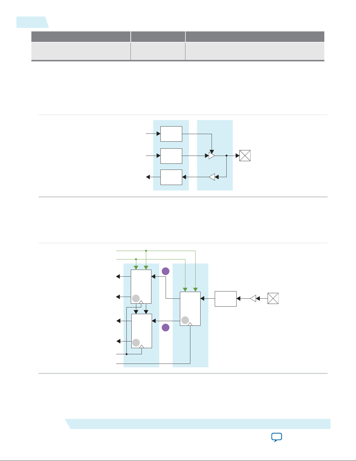
The following figure shows the simplified view of a single-ended GPIO input path.
Figure 2: Input Path (Simplified View)
The pad sends data to the input buffer, and the input buffer feeds the delay element.
Altera GPIO IP Core User Guide
Send Feedback
Page 5

ug-altera_gpio
2014.08.18
Input Path Waveform
5
Note: The Altera GPIO megafunction does not support dynamic calibration of the input path. For
applications requiring dynamic calibration of the input path, refer to the Altera PHYLite
Megafunction User Guide.
After data goes to the output of the delay element, programmable bypass multiplexers select the features
and paths to use. Each input path contains two stages of DDIOs, which are full-rate and half-rate.
Note: When you set the Register mode option to Simple register, the full-rate DDIO works as a simple
register.
Note: When you set the Register mode option to Simple register, the Fitter chooses whether to pack the
register in the I/O or implement the register in the core, depending on the area and timing tradeoffs.
Use the input path in four modes:
• Bypass—data goes from the delay element to the core, bypassing all DDIOs.
• Packed Register—the full-rate DDIO operates as a register, bypassing half-rate DDIOs.
• Double data rate Input/Output (DDIO) mode with full-rate conversion—The full-rate DDIO operates
as a regular DDIO, bypassing half-rate DDIOs.
• DDIO mode with half-rate conversion—The full-rate DDIO operates as a regular DDIO. Half-rate
DDIOs converts data for full-rate to half-rate.
All DDIOs share the same asynchronous clear and preset signals when used. Half-rate and full-rate
DDIOs connect to separate clocks. When you use half-rate and full-rate DDIOs, the full-rate clock must
run at twice the half-rate frequency. Use different phase relationships to meet timing requirements.
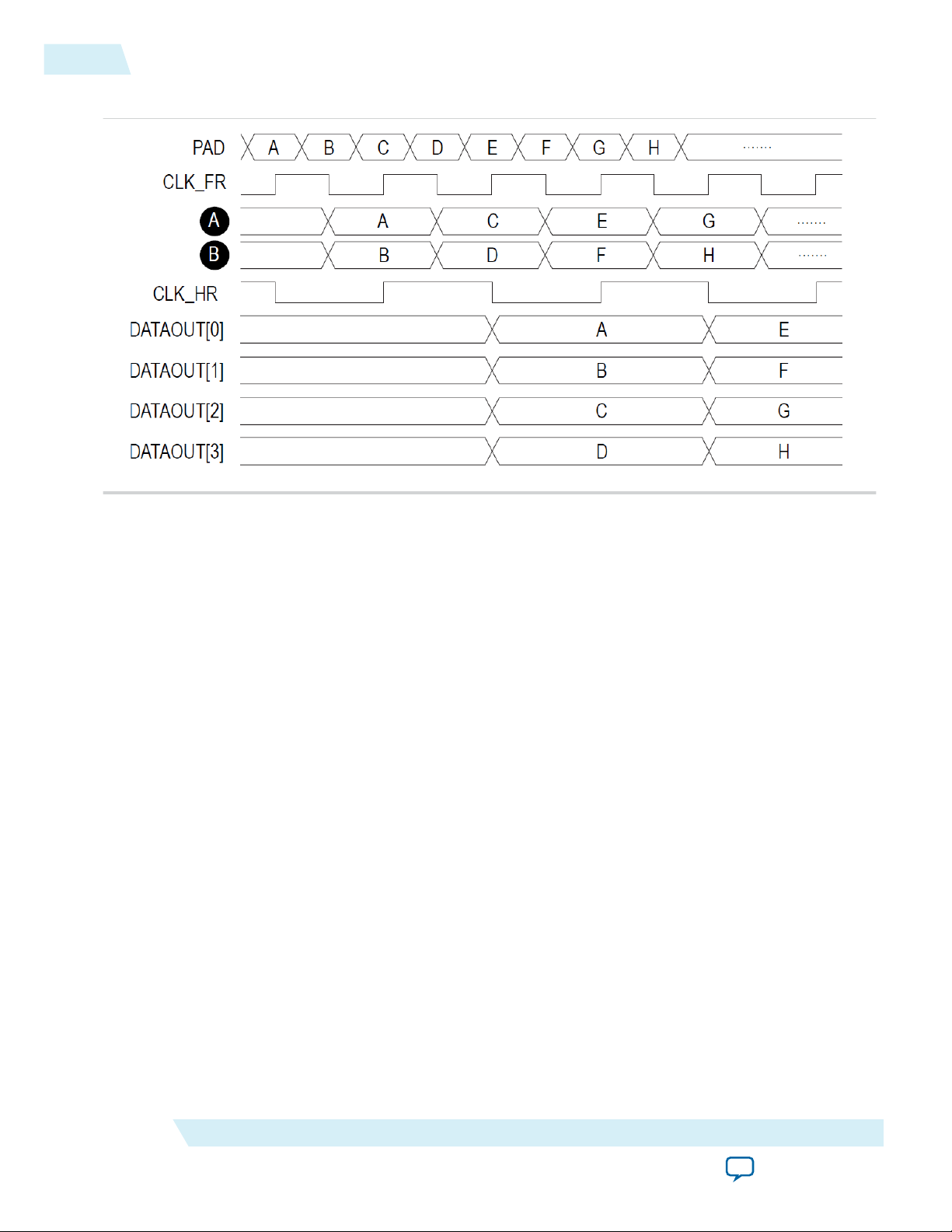
Input Path Waveform
The following figure shows the waveforms for an input path in DDIO mode with half-rate conversion.
This configuration uses all the blocks and refers to the same labels shown in Figure 2.
Note:
The actual timing relationship between different signals may vary depending on the specific design,
delays, and phases that you choose for the full-rate and half-rate clocks.
Altera GPIO IP Core User Guide
Send Feedback
Altera Corporation
Page 6
6
Output Path
Figure 3: Input Path Waveform
ug-altera_gpio
2014.08.18
The pad receives data. DDIO IN (1) (refer to Figure 2) captures data on the rising and falling edges of
CLK_FR, and sends data at SDR (refer to signals (A) and (B) in the waveform). DDIO IN (2) and DDIO
IN (3) (refer to Figure 2) halves the data rate and DATAOUT[3:0] presents data as a half-rate bus.
Notice how going from full-rate clock at double data rate to half-rate clock at single data rate, data rate has
been divided by four and the bus size has increased by the same ratio. The overall throughput through the
Altera GPIO IP core remained unchanged.
Output Path
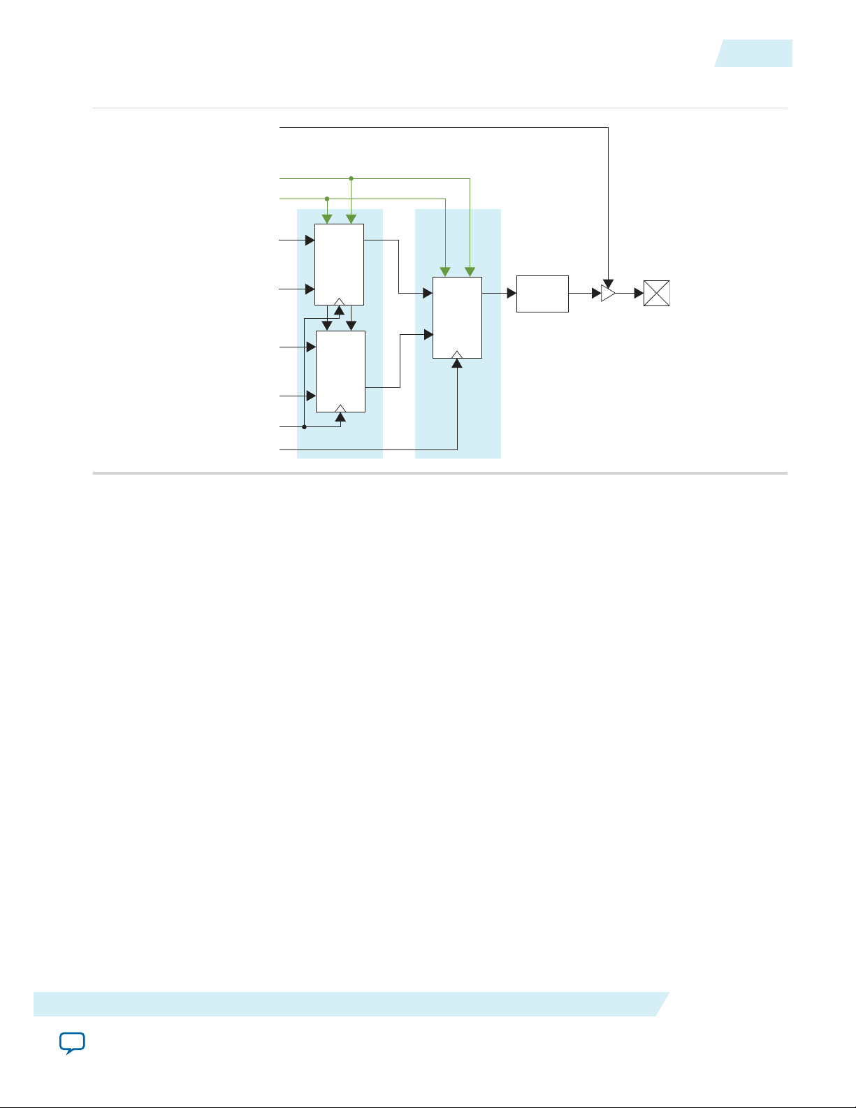
The following figure shows the simplified view of a single-ended GPIO output path.
Altera Corporation
Altera GPIO IP Core User Guide
Send Feedback
Page 7
PAD
ACLR_N
APRE_N
DATAOUT[0]
DATAOUT[2]
DATAOUT[1]
DATAOUT[3]
CLK_HR
CLK_FR
DDIO
OUT
DDIO
OUT
DDIO
OUT
Delay
Element
HR FR
OE
from Output
Enable Path
ug-altera_gpio
2014.08.18
Figure 4: Output Path (Simplified View)
Output Path
7
The simplified view of a GPIO output path is similar to the input path (refer to Figure 2). The output
delay element sends data to the pad through the output buffer.
Note:
The Altera GPIO IP core does not support dynamic calibration of the input path. For applications
requiring dynamic calibration of the output path, refer to the Altera PHYLite Megafunction User
Guide.
Note: When you set the Register mode option to Simple register, the full-rate DDIO works as a simple
register.
Note: When you set the Register Mode option to Simple register, the Fitter chooses whether to pack the
register in the I/O or implement the register in the core, depending on the area and timing tradeoffs.
You can select a combination of half-rate, full-rate DDIOs, and simple register using programmable
bypass multiplexers to implement the following four output modes:
• Bypass—data goes from the core straight to the delay element, bypassing all DDIOs.
• Packed Register—full-rate DDIO operates as a register, bypassing half-rate DDIOs.
• DDIO output mode, Full-Rate—full-rate DDIO operates as a regular DDIO, bypassing half-rate
DDIOs.
• DDIO output, Half-Rate—full-rate DDIO operates as a regular DDIO. Half-rate DDIOs convert data
from full-rate to half-rate.
All DDIOs share the same asynchronous clear and preset signals when used. Half-rate and full-rate
DDIOs connect to separate clocks. When you use half-rate and full-rate DDIOs, the full-rate clock must
run at twice the half-rate frequency. You can use different phase relationships to meet timing require‐
ments.
Altera GPIO IP Core User Guide
Send Feedback
Altera Corporation
Page 8

ACLR_N
APRE_N
OEIN[0]
OEIN[1]
CLK_HR
CLK_FR
DDIO
OUT
FF Delay
Element
HR FR
From Output
Data Path
Pad
Data
Clock
Altera GPIO
Termination
Reset
8
Output Path Waveform
Output Path Waveform
The waveform for the output path is similar to Figure 3.
OE Path
The following figure shows the simplified view of a GPIO OE path.
Figure 5: OE Path (Simplified View)
ug-altera_gpio
2014.08.18
The simplified view of a GPIO OE path is similar to the Figure 4. The difference between output path and
OE path is that the OE path does not support full-rate DDIO mode. Therefore, there is no full-rate DDIO
in OE path. To support packed-register implementations in the OE path, a simple register operates as fullrate DDIO. For the same reason, there is no need for two half-rate DDIOs. Only one is present.
The OE path operates in the following three fundamental modes:
• Bypass—the core sends data directly to the delay element, bypassing all DDIOs.
• Packed Register—bypasses half-rate DDIO.
• SDR output, half-rate—half-rate DDIOs convert data from full-rate to half-rate.
Interfaces
The following figure shows the main interfaces for the Altera GPIO IP core.
Figure 6: Altera GPIO IP Core Interfaces Diagram
Altera Corporation
Altera GPIO IP Core User Guide
Send Feedback
Page 9

din
pad_out
pad_in
oe
pad_io
pad_io_b
pad_out_b
ck
sclr
aclr
aset
sset
ck_fr
ck_hr
ck_fr_in
ck_fr_out
ck_hr_in
ck_hr_out
Altera GPIO
ck_out
ck_in
seriesterminationcontrol
parallelterminationcontrol
dout
Pad Interface Signals
cke
pad_in_b
Reset Interface Signals
Termination Interface Signals
Data Interface Signals
Clock Interface Signals
ug-altera_gpio
2014.08.18
The following table lists the Altera GPIO IP core main interfaces:
Table 2: Altera GPIO IP Core Interfaces
Interface Description
Pad Interface Connects the Altera GPIO IP core to the pads. This interface can be an input,
Data Interface An input and/or output interface to the core. Consists of different signals,
Clock Interface An input clock interface. Consists of different signals, depending on the
Termination Interface Connects the Altera GPIO IP core to the buffers.
Reset Interface Connects the Altera GPIO IP core to the DDIOs.
Interface Signals
output or bidirectional interface, depending on the configuration of the
Altera GPIO IP core.
depending on the configuration of the Altera GPIO IP core.
configuration of the Altera GPIO IP core. The Altera GPIO IP core can have
0, 1, 2 or 4 clock inputs depending on the configuration. Clock ports appear
differently in different configurations, to reflect the actual function
performed by the clock signal.
9
Interface Signals
The following figure list the signals for the data, clock, termination, reset, and pad interfaces.
Pad Interface Signals
Pad interface is the physical connection from the Altera GPIO IP core to the pad. When you configure the
Altera GPIO IP core as an output, the pad signal in an output signal. When you configure the Altera
GPIO IP core as an input, the pad signal is an input signal. When you configure the Altera GPIO IP core
as bidirectional, the pad signal is a bidirectional signal.
Altera GPIO IP Core User Guide
SIZE is the data width selected from the GUI.
Send Feedback
Altera Corporation
Page 10

10
Data Interface Signals
Signal Name Direction Description
pad_in[SIZE -1:0] Input Input pad port only when the input path is used.
pad_in_b[SIZE -1:0] Input Input negative pad port only when input path is
used, and differential buffers are enabled.
pad_out[SIZE -1:0] Output Output pad port only when output path is used.
pad_out_b[SIZE -1:0] Output Output negative pad port only when output path is
used, and differential buffers are enabled.
pad_io[SIZE -1:0] Bidirectional Bidirectional pad port only when bidirectional paths
are used.
pad_io_b[SIZE -1:0] Bidirectional Bidirectional negative pad port only when bidirec‐
tional paths are used, and differential buffers are
enabled.
Data Interface Signals
Signal Name Direction Description
ug-altera_gpio
2014.08.18
din[DATA_SIZE - 1 : 0] Input
Data connection from the core to the Altera GPIO
IP core when in output or bidirectional mode. This
interface is not present in input mode.
DATA_SIZE has different values, depending on the
Altera GPIO configuration:
• Combinational or packed register— DATA_SIZE
= SIZE
• DDIO, no half-rate logic— DATA_SIZE = 2 x
SIZE
• DDIO with half-rate logic—DATA_SIZE = 4 x
SIZE
dout[DATA_SIZE - 1 : 0] Output Data connection from the Altera GPIO IP core to
the core when in input or bidirectional mode. This
interface is not present in output mode. DATA_
SIZE has different values depending on the Altera
GPIO configuration:
• Combinational or packed register—DATA_SIZE
= SIZE
• DDIO, no half-rate logic—DATA_SIZE = 2 x
SIZE
• DDIO with half-rate logic— DATA_SIZE = 4 x
SIZE
Altera Corporation
Altera GPIO IP Core User Guide
Send Feedback
Page 11

SIZE - 1 ... 0
t
3
SIZE - 1 ... 0
t
2
SIZE - 1 ... 0
t
1
SIZE - 1 ... 0
t
0
4 x SIZE
SIZE - 1 ... 0
t
1
SIZE - 1 ... 0
t
0
2 x SIZE
SIZE - 1 ... 0 SIZE
ug-altera_gpio
2014.08.18
Data Bit-Order for Data Interface
Signal Name Direction Description
oe[OE_SIZE - 1 : 0] Input OE connection from the core to the Altera GPIO
IP core when in bidirectional mode or in output
mode if you enable the use output enable port
parameter. OE is active high.
Set this signal to '1' when transmitting data and set
this signal to '0' when receiving data. This interface
is not present in input mode.
OE_SIZE has different values depending on
whether the Altera GPIO configuration:
• Combinational or packed register— DATA_SIZE
= SIZE
• DDIO, no half-rate logic— DATA_SIZE = SIZE
• DDIO with half-rate logic— DATA_SIZE = 2 x
SIZE
Data Bit-Order for Data Interface
The din, dout and oe data signals follow the following bit-order convention.
11
Figure 7: Data Bit-Order
Where:
• If the data bus has the size value of SIZE, the LSB is at the right-most position.
• If the data bus has the size value of 2 x SIZE, it will be made of 2 words of SIZE .
• If the data bus has the size value of 4 x SIZE, it will be made of 4 words of SIZE.
• The LSB is in the right-most position for each word.
• The right-most word specifies the first word going out for output buses and the first word coming in
for input buses.
Note:
Refer to Figure 3.
Altera GPIO IP Core User Guide
Send Feedback
Altera Corporation
Page 12

12
Clock Interface Signals
Clock Interface Signals
Signal Name Direction Description
ck Input This clock feeds a packed register or DDIO in input and output
paths when half-rate DDIOs are not used. If the Altera GPIO IP
core is in bidirectional mode and if you turn off the Separate
Input/Output Clocks parameter, this is the unique clock for
input and output paths.
ug-altera_gpio
2014.08.18
ck_fr
ck_hr
Input
These clocks feed full-rate and half-rate DDIO in both input and
output paths when half-rate DDIOs are used. If the Altera GPIO
IP core is in bidirectional mode and if you turn off the Separate
Input/Output Clocks parameter, the input and output paths use
these clocks.
ck_in
ck_out
Input
These clocks feed a packed register or DDIO in the input and
output path of a bidirectional Altera GPIO when half-rate
DDIOs are not used, and separate clocks are requested by
turning on the Separate Input/Output Clocks parameter.
ck_fr_in
ck_fr_out
Input
ck_hr_in
ck_hr_out
cke Input Clock enable.
These clocks feed full-rate and half-rate DDIOs in the input and
output paths of a bidirectional Altera GPIO when half-rate
DDIOs are used, and separate clocks are requested by turning on
the Separate Input/Output Clocks parameter. For example, ck_
fr_out feeds the full-rate DDIO in the output path.
Termination Interface Signals
Signal Name Direction Description
seriesterminationcontrol Input Input from the termination control block
(OCT) to the buffers. It sets the buffer series
impedance value.
parallelterminationcontrol Input Input from the termination control block
Reset Interface Signals
sclr Input Synchronous clear.
aclr Input Asynchronous clear.
aset Input Asynchronous set.
sset Input Synchronous set.
Shared Signals
The input, output, and OE paths share the same clear and preset signals.
The output and OE path shares the same clock signals.
Altera Corporation
(OCT) to the buffers. It sets the buffer
parallel impedance value.
Signal Name Direction Description
Altera GPIO IP Core User Guide
Send Feedback
Page 13

ug-altera_gpio
2014.08.18
Data Interface Signals and Corresponding Clocks
The following table shows the data interface signals and the corresponding clocks.
Table 3: Data Interface Signals and Corresponding Clocks
Signal Name Configuration Clock
Register Mode: Simple
Register/DDIO
Half-rate: not used
Separate Clocks: Off
Register Mode: DDIO
Data Interface Signals and Corresponding Clocks
ck
ck_hrHalf rate: used
13
din
dout/oe
Separate Clocks: off
Register Mode: Simple
Register/DDIO
Half rate: not used
Separate Clocks: on
Register Mode: DDIO
Separate Clocks: on
Register Mode: Simple
Register/DDIO
Half rate: not used
Separate Clocks: off
Register Mode: DDIO
Separate Clocks: off
Register Mode: Simple
Register/DDIO
Half rate: not used
ck_in
ck_hr_inHalf rate: used
ck
ck_hrHalf rate: used
ck_out
Altera GPIO IP Core User Guide
Send Feedback
Separate Clocks: on
Register Mode: DDIO
ck_hr_outHalf rate: used
Separate Clocks: on
Altera Corporation
Page 14

14
Register Packing
Signal Name Configuration Clock
Register Mode: Simple
Register/DDIO
Half rate: not used
ck
Separate Clocks: off
Register Mode: DDIO
ck_frHalf rate: used
Separate Clocks: off
ug-altera_gpio
2014.08.18
sclr/sset/ all pad signals
Register Mode: Simple
Register/DDIO
Half rate: not used
Separate Clocks: on
Register Mode: DDIO
Half rate: used
Separate Clocks: on
Register Packing
The Altera GPIO IP core allows you to pack register into the periphery to save area and resource utiliza‐
tion.
You can configure the full-rate DDIO on the input and output path as a flip flop. To do so, add the .qsf
assignments listed in this table.
Table 4: Register Packing QSF Assignments
Path QSF Assignment
• Input path: ck_in
• Output path: ck_out
• Input path: ck_fr_in
• Output path: ck_fr_out
Input register packing set_instance_assignment -name FAST_INPUT_REGISTER ON -to <path to
Output register
packing
Output enable
register packing
Note: These assignments do not guarantee register packing but rather enable the Fitter to find a legal
placement. Otherwise, the Fitter will keep the flip flop in the core.
Altera GPIO Timing
The Quartus II software version 14.0a10 does not automatically generate the timing constraints.
Altera Corporation
register>
set_instance_assignment -name FAST_OUTPUT_REGISTER ON -to <path to
register>
set_instance_assignment -name FAST_OUTPUT_ENABLE_REGISTER ON -to
<path to register>
Altera GPIO IP Core User Guide
Send Feedback
Page 15

PAD
ACLR_N
APRE_N
DATAOUT[0]
DATAOUT[2]
DATAOUT[1]
DATAOUT[3]
CLK_HR
CLK_FR
DDIO
IN
DDIO
IN
DDIO
IN
Delay
Element
HR FR
B
A
1
3
2
I/O Path
Core Interface Data Path
Core Interface Clock Path
Full-rate/Half-rate Transfer Path
ug-altera_gpio
2014.08.18
Altera GPIO Timing Components
The following paths are the timing components for Altera GPIO IP core:
• I/O interface paths (from FPGA to external receiving devices and from external transmitting devices to
FPGA)
• Core interface paths of the data and the clock (from I/O to core and from core to I/O)
• Half-rate to full-rate and full-rate to half-rate transfer paths.
Note: The TimeQuest timing analyzer treats the path inside the DDIO_IN and DDIO_OUT blocks as
black boxes.
These figures show the timing components in the Altera GPIO input, output, and output enable paths.
Figure 8: Timing Components in the Altera GPIO Input Path
Altera GPIO Timing Components
15
Altera GPIO IP Core User Guide
Send Feedback
Altera Corporation
Page 16

PAD
ACLR_N
APRE_N
DATAOUT[0]
DATAOUT[2]
DATAOUT[1]
DATAOUT[3]
CLK_HR
CLK_FR
DDIO
OUT
DDIO
OUT
DDIO
OUT
Delay
Element
HR FR
OE
from Output
Enable Path
Half-rate/Full-rate Transfer Path
I/O Path
Core Interface Clock Path
Core Interface Data Path
ACLR_N
APRE_N
OEIN[0]
OEIN[1]
CLK_HR
CLK_FR
DDIO
OUT
FF
Delay
Element
HR FR
From Output
Data Path
Half-rate/Full-rate Transfer Path
Core Interface Data Path
Core Interface Clock Path
I/O Path
16
Timing Analysis
Figure 9: Timing Components in the Altera GPIO Output Path
ug-altera_gpio
2014.08.18
Figure 10: Timing Components in the Altera GPIO Output Enable Path
Timing Analysis
Altera Corporation
The Quartus II software does not automatically generate the SDC timing constraints for Altera GPIO IP
core. You must manually enter the timing constraints. This section provides simple instructions and
examples on how to timing constrain the Altera GPIO IP core to ensure that the TimeQuest Timing
Analyzer analyzes the I/O timing correctly.
Altera GPIO IP Core User Guide
Send Feedback
Page 17

ug-altera_gpio
2014.08.18
Related Information
• AN 433: Constraining and Analyzing Source-Synchronous Interfaces
Describes techniques for constraining and analyzing source-synchronous interfaces.
Core Interface Path Timing Analysis
To properly perform timing analysis for the core interface paths, you must define the clock settings in
the .sdc for the following:
• clock to the core registers and
• clock to the I/O registers (Simple register and DDIO mode)
To properly perform timing analysis for the I/O interface, specify the system level constraints of the data
pins against the system clock pin in the .sdc.
Single Data Rate Input Register
Figure 11: Single Data Rate Input Register
Core Interface Path Timing Analysis
17
This SDC command creates the clock setting for the input clock:
create_clock -name sdr_in_clk -period "100 MHz" sdr_in_clk
This command instructs the TimeQuest timing analyzer to timing analyze the input I/O with 0.15 ns
input delay.
set_input_delay -clock sdr_in_clk 0.15 sdr_in_data
Altera GPIO IP Core User Guide
Altera Corporation
Send Feedback
Page 18

Outside FPGA
FPGA
18
DDIO Input Register (Full-Rate or Half-Rate)
DDIO Input Register (Full-Rate or Half-Rate)
Figure 12: DDIO Input Register (Full-Rate or Half-Rate)
The input side of full-rate and half-rate DDIO is the same. You can properly constrain the system by
using a virtual clock to model the off-chip transmitter to the FPGA.
ug-altera_gpio
2014.08.18
create_clock
These SDC commands create the clock settings for the virtual and the DDIO clock.
create_clock -name virtual_clock -period "200 MHz"
create_clock -name ddio_in_clk -period "200 MHz" ddio_in_clk
set_input_delay
These set_input_delay commands instruct the TimeQuest timing analyzer to analyze the positive clock
edge and the negative clock edge of the transfer. Note the "-add_delay" in the second set_input_delay
command:
set_input_delay -clock virtual_clock 0.25 ddio_in_data
set_input_delay -add_delay -clock_fall -clock virtual_clock 0.25 ddio_in_data
set_false_path
These set_false_path commands instruct the TimeQuest timing analyzer to ignore the positive clock
edge to the negative edge triggered register and the negative clock edge to the positive edge triggered
register:
Altera Corporation
set_false_path -fall_from virtual_clock -rise_to ddio_in_clk
set_false_path -rise_from virtual_clock -fall_to ddio_in_clk
Altera GPIO IP Core User Guide
Send Feedback
Page 19

ug-altera_gpio
2014.08.18
Single Data Rate Output Register
Note: The CLK_HR frequency must be half the frequency of CLK_FR. If the clocks are driven by IOPLL,
you may consider using the derive_pll_clocks SDC command.
Single Data Rate Output Register
Figure 13: Single Data Rate Output Register
19
These SDC commands generate the source clock and the output clock to be transmitted:
create_clock -name sdr_out_clk -period "100 MHz" sdr_out_clk
create_generated_clock -source sdr_out_clk -name sdr_out_outclk sdr_out_outclk
This SDC command instructs the TimeQuest timing analyzer to analyze the output data to be transmitted
against the output clock to be transmitted.
set_output_delay -clock sdr_out_clk 0.45 sdr_out_data
DDIO Output Register
The output side of the full-rate and half-rate DDIO output register is the same.
create_clock and create_generated_clock
These SDC commands generate the clocks to the DDIO and the clock to be transmitted:
create_clock -name ddio_out_fr_clk -period "200 MHz" ddio_out_fr_clk
create_generated_clock -source ddio_out_fr_clk -name ddio_out_fr_outclk
ddio_out_fr_outclk
Altera GPIO IP Core User Guide
Send Feedback
Altera Corporation
Page 20

20
Altera GPIO Delay Elements
set_output_delay
These commands instruct the TimeQuest Timing Analyzer to timing analyze the positive data and the
negative data against the output clock
set_output_delay -clock ddio_out_fr_outclk 0.55 ddio_out_fr_data
set_output_delay -add_delay -clock_fall -clock ddio_out_fr_outclk 0.55
ddio_out_fr_data
set_false_path
You need these set_false_path commands to stop the TimeQuest timing anaylzer from timing analyzing
the rising edge of the source clock against the falling edge of the output clock and the falling edge of
source clock against rising edge of output clock:
set_false_path -rise_from ddio_out_fr_clk -fall_to ddio_out_fr_outclk
set_false_path -fall_from ddio_out_fr_clk -rise_to ddio_out_fr_outclk
Altera GPIO Delay Elements
ug-altera_gpio
2014.08.18
The Quartus II software version 14.0a10 does not support automatic setting of delay elements to
maximize slack of I/O timing analysis. You must manually set the delay elements through QSF settings to
close timing or maximize slack on the I/O timing analysis.
You can access the delay elements using these QSF assignments:
Table 5: QSF Assignments for Altera GPIO Delay Elements
Delay Element QSF Assignments
Input Delay Element
Output Delay Element
Output Enable Delay
Element
set_intance_assignment –to <PIN> -name INPUT_DELAY_CHAIN
<0..63>
set_intance_assignment –to <PIN> -name OUTPUT_DELAY_CHAIN
<0..15>
set_intance_assignment –to <PIN> -name OE_DELAY_CHAIN
<0..15>
Timing Closure Guideline
For the input registers of the Altera GPIO IP core, if you do not set the input delay chain, it is likely the
input I/O transfer will fail hold time, because the clock delay is larger than the data delay. In such cases,
use the input delay chain to add delay to the input data path to meet hold time. As a general guide, the
input delay chain is about 60 ps per step at -1 speed grade. Dividing the negative hold slack by 60 ps
provides an approximate input delay chain setting to set to pass timing.
However, if the clocks of the GPIO input registers (simple register mode or DDIO mode) are driven by an
I/O phase locked loop (IOPLL), you can choose to set the compensation mode to source synchronous
Altera Corporation
Altera GPIO IP Core User Guide
Send Feedback
Page 21

ug-altera_gpio
2014.08.18
mode. The Fitter will attempt to configure the IOPLL for a better setup and hold slack of the input I/O
timing analysis.
For the output and output enable registers of the Altera GPIO IP core, you can use the output delay chain
and output enable delay chain to add delay to the output data and the output clock. If setup time violation
is observed, you can increase the delay chain setting of the output clock. If hold time violation is observed,
you can increase the delay chain setting of output data.
Design Example
The Altera GPIO IP core is able to generate a design example that matches the same configuration chosen
for the IP. The design example is a simple design that does not target any specific application; however
you can use the design example as a reference on how to instantiate the IP core and what behavior to
expect in a simulation.
Note: The .qsys files are for internal use during example design generation only. You cannot edit the files.
Generating Design Example
During generation, the Generation dialog box displays the option to generate a design example. Turn on
the Generate Example Design option.
Design Example
21
The software generates the <instance>_example_design directory along with the IP, where <instance> is
the name of your IP.
The <instance>_example_design directory contains two TCL scripts:
• - make_qii_design.tcl
• - make_sim_design.tcl
Generating Quartus Design Example
The make_qii_design.tcl generates a synthesizable design example along with a Quartus project, ready
for compilation.
To generate synthesizable design example, run the following script at the end of IP generation:
quartus_sh -t make_qii_design.tcl
To specify an exact device to use, run the following script:
quartus_sh -t make_qii_design.tcl [device_name]
This script generates a qii directory containing a project called ed_synth.qpf. You can open and compile
this project with the Quartus II software.
Generating Simulation Design Example
The make_sim_design.tcl generates a simulation design example along with tool-specific scripts to
compile and elaborate the necessary files.
To generate a simulation design example, run the following script at the end of IP generation:
quartus_sh -t make_sim_design.tcl
Altera GPIO IP Core User Guide
Send Feedback
Altera Corporation
Page 22

22
Document Revision History
To generate simulation design example for a VHDL-only simulator, run the following script:
quartus_sh -t make_sim_design.tcl VHDL
This script generates a sim directory containing one subdirectory for each supported simulation tools.
Each subdirectory contains the specific scripts to run simulation with the corresponding tool.
The simulation design example is made of a driver connected to the generated IP. The driver generates
random traffic and internally checks the legality of the out going data.
Document Revision History
Date Version Changes
ug-altera_gpio
2014.08.18
August, 2014 2014.08.18
November,
2013.11.29 Initial release.
2013
• Added timing information.
• Added register packing information.
• Added Use legacy top-level port names parameter. This is a new
parameter.
• Added register packing information.
• Replaced the term megafunction with IP core.
Altera Corporation
Altera GPIO IP Core User Guide
Send Feedback
 Loading...