

Page 1
查询EPF81188A供应商查询EPF81188A供应商
FLEX 8000
®
Programmable Logic
Device Family
September 1998, ver. 9.11 Data Sheet
Low-cost, high-density, register-rich CMOS programmable logic
Features...
■
device (PLD) family (see Table 1)
– 2,500 to 16,000 usable gates
– 282 to 1,500 registers
System-level features
■
– In-circuit reconfigurability (ICR) via external Configuration
EPROM or intelligent controller
– Fully compliant with the peripheral component interconnect
(PCI) standard
– Built-in Joint-Test Action Group (JTAG) boundary-scan test (BST)
circuitry compliant with IEEE Std. 1149.1-1990 on selected devices
– MultiVolt
while I/O pins are compatible with 5.0-V and 3.3-V logic levels
– Low power consumption (typical specification less than 0.5 mA
in standby mode)
Flexible interconnect
■
– FastTrack
predictable interconnect delays
– Dedicated carry chain that implements arithmetic functions such
as fast adders, counters, and comparators (automatically used by
software tools and megafunctions)
– Dedicated cascade chain that implements high-speed, high-fan-in
logic functions (automatically used by software tools and
megafunctions)
– Tri-state emulation that implements internal tri-state nets
Powerful I/O pins
■
– Programmable output slew-rate control reduces switching noise
Peripheral register for fast setup and clock-to-output delay
■
™
I/O interface enabling device core to run at 5.0 V,
™
Interconnect continuous routing structure for fast,
3
FLEX 8000
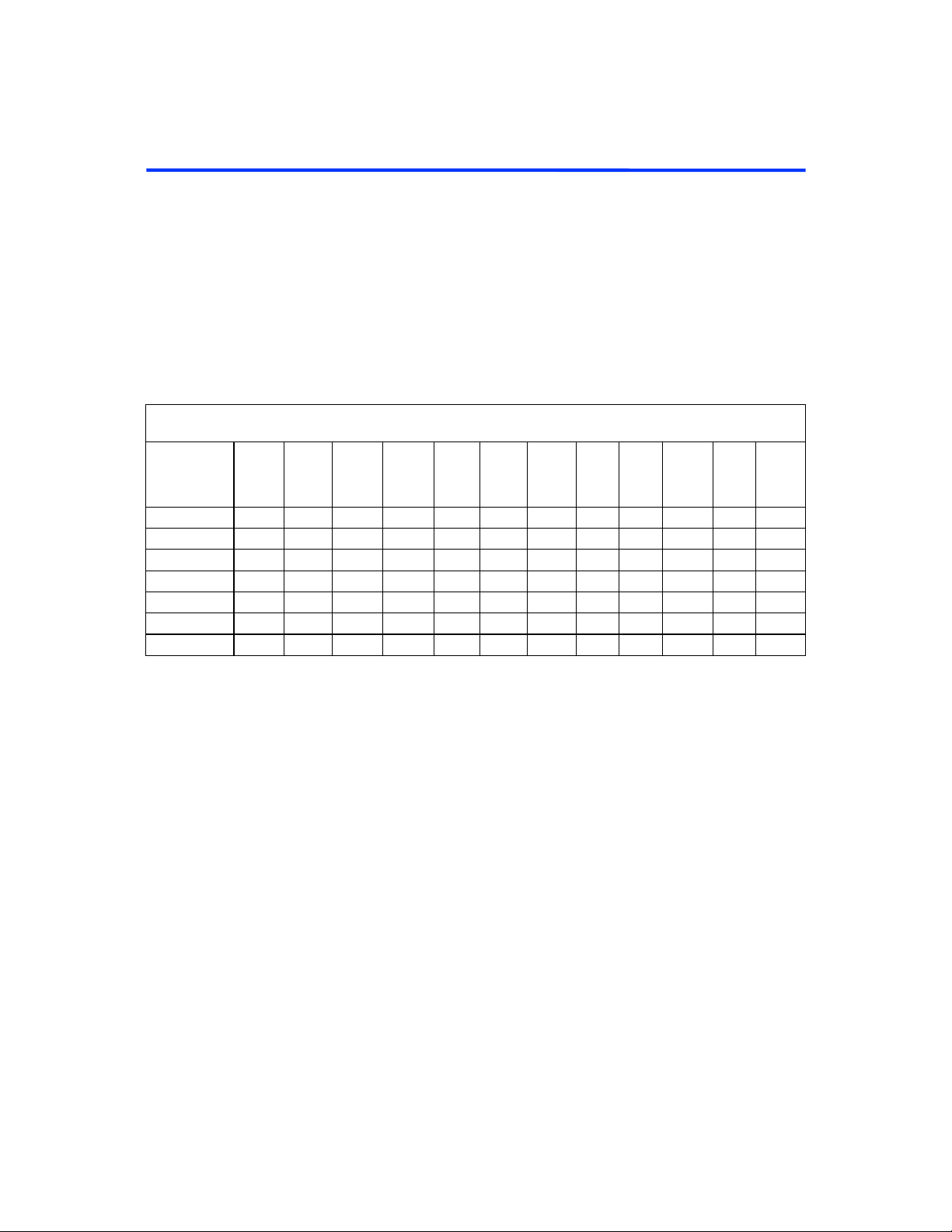
Table 1. FLEX 8000 Device Features
Feature EPF8282A
EPF8282AV
Usable gates 2,500 4,000 6,000 8,000 12,000 16,000
Flipflops 282 452 636 820 1,188 1,500
Logic array blocks (LABs) 26 42 63 84 126 162
Logic elements (LEs) 208 336 504 672 1,008 1,296
Maximum user I/O pins 78 120 136 152 184 208
JTAG BST circuitry Yes No Yes Yes No Yes
Altera Corporation 1
A-DS-F8000-09.11
EPF8452A EPF8636A EPF8820A EPF81188A EPF81500A
Page 2
FLEX 8000 Programmable Logic Device Family Data Sheet
■
...and More
Features
Fabricated on an advanced SRAM process
■
Available in a variety of packages with 84 to 304 pins (see Table 2)
■
Software design support and automatic place-and-route provided by
the Altera
®
MAX+PLUS
Pentium-based PCs, and Sun SPARCstation, HP 9000 Series 700/800,
and IBM RISC System/6000 workstations
■
Additional design entry and simulation support provided by EDIF
2 0 0 and 3 0 0 netlist files, library of parameterized modules (LPM),
Verilog HDL, VHDL, and other interfaces to popular EDA tools from
manufacturers such as Cadence, Exemplar Logic, Mentor Graphics,
OrCAD, Synopsys, Synplicity, and Veribest
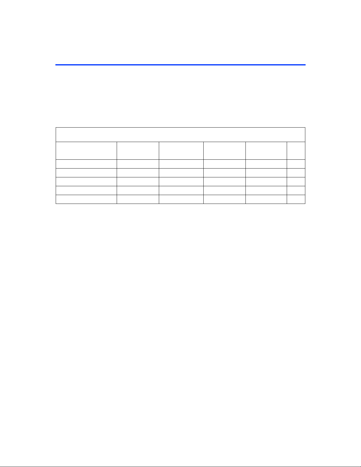
Table 2. FLEX 8000 Package Options & I/O Pin Count Note (1)
®
II development system for 486- and
Device 84-Pin
PLCC
EPF8282A 68 78
EPF8282AV 78
EPF8452A 68 68 120 120
EPF8636A 68 118 136 136
EPF8820A 112 120 152 152 152
EPF81188A 148 184 184
EPF81500A 181 208 208
Note:
(1) FLEX 8000 device package types include plastic J-lead chip carrier (PLCC), thin quad flat pack (TQFP), plastic quad
flat pack (PQFP), power quad flat pack (RQFP), ball-grid array (BGA), and pin-grid array (PGA) packages.
General
Description
100-
TQFP
Pin
144-
Pin
TQFP
160-
Pin
PQFP
160-
Pin
PGA
192-
Pin
PGA
208-
Pin
PQFP
Altera’s Flexible Logic Element MatriX (FLEX
225-
Pin
BGA
232-
PGA
®
240-
280-
Pin
Pin
PQFP
Pin
PGA
) family combines the
benefits of both erasable programmable logic devices (EPLDs) and fieldprogrammable gate arrays (FPGAs). The FLEX 8000 device family is ideal
304-
Pin
RQFP
for a variety of applications because it combines the fine-grained
architecture and high register count characteristics of FPGAs with the
high speed and predictable interconnect delays of EPLDs. Logic is
implemented in LEs that include compact 4-input look-up tables (LUTs)
and programmable registers. High performance is provided by a fast,
continuous network of routing resources.
2 Altera Corporation
Page 3
FLEX 8000 devices provide a large number of storage elements for
applications such as digital signal processing (DSP), wide-data-path
manipulation, and data transformation. These devices are an excellent
choice for bus interfaces, TTL integration, coprocessor functions, and
high-speed controllers. The high-pin-count packages can integrate
multiple 32-bit buses into a single device. Table 3 shows FLEX 8000
performance and LE requirements for typical applications.
Table 3. FLEX 8000 Performance
FLEX 8000 Programmable Logic Device Family Data Sheet
Application LEs Used A-2 Speed Grade A-3 Speed Grade A-4 Speed
16-bit loadable counter
16-bit up/down counter
24-bit accumulator
16-bit address decode
16-to-1 multiplexer
16
16
24
10
125 95 83 MHz
125 95 83 MHz
87 67 58 MHz
4
4.2 4.9 6.3 ns
6.6 7.9 9.5 ns
All FLEX 8000 device packages provide four dedicated inputs for
synchronous control signals with large fan-outs. Each I/O pin has an
associated register on the periphery of the device. As outputs, these
registers provide fast clock-to-output times; as inputs, they offer quick
setup times.
The logic and interconnections in the FLEX 8000 architecture are
configured with CMOS SRAM elements. FLEX 8000 devices are
configured at system power-up with data stored in an industry-standard
parallel EPROM or an Altera serial Configuration EPROM device, or with
data provided by a system controller. Altera offers the EPC1, EPC1213,
EPC1064, and EPC1441 Configuration EPROMs, which configure
FLEX 8000 devices via a serial data stream. Configuration data can also be
stored in an industry-standard 32 K × 8 bit or larger EPROM, or
downloaded from system RAM. After a FLEX 8000 device has been
configured, it can be reconfigured in-circuit by resetting the device and
loading new data. Because reconfiguration requires less than 100 ms, realtime changes can be made during system operation.
Units
Grade
3
FLEX 8000
f
Altera Corporation 3
For information on how to configure FLEX 8000 devices, go to the
following documents:
Configuration EPROMs for FLEX Devices Data Sheet
■
BitBlaster Serial Download Cable Data Sheet
■
ByteBlaster Parallel Port Download Cable Data Sheet
■
Application Note 33 (Configuring FLEX 8000 Devices)
■
Application Note 38 (Configuring Multiple FLEX 8000 Devices)
■
Page 4

FLEX 8000 Programmable Logic Device Family Data Sheet
FLEX 8000 devices contain an optimized microprocessor interface that
permits the microprocessor to configure FLEX 8000 devices serially, in
parallel, synchronously, or asynchronously. The interface also enables the
microprocessor to treat a FLEX 8000 device as memory and configure the
device by writing to a virtual memory location, making it very easy for the
designer to create configuration software.
The FLEX 8000 family is supported by Altera’s MAX+PLUS II
development system, a single, integrated package that offers schematic,
text—including the Altera Hardware Description Language (AHDL),
VHDL, and Verilog HDL—and waveform design entry; compilation and
logic synthesis; simulation and timing analysis; and device programming.
The MAX+PLUS II software provides EDIF 2 0 0 and 3 0 0, library of
parameterized modules (LPM), VHDL, Verilog HDL, and other interfaces
for additional design entry and simulation support from other industrystandard PC- and UNIX workstation-based EDA tools. The
MAX+PLUS II software runs on 486- and Pentium-based PCs, and Sun
SPARCstation, HP 9000 Series 700/800, and IBM RISC System/6000
workstations.
f
Functional
Description
The MAX+PLUS II software interfaces easily with common gate array
EDA tools for synthesis and simulation. For example, the MAX+PLUS II
software can generate Verilog HDL files for simulation with tools such as
Cadence Verilog-XL. Additionally, the MAX+PLUS II software contains
EDA libraries that use device-specific features such as carry chains, which
are used for fast counter and arithmetic functions. For instance, the
Synopsys Design Compiler library supplied with the MAX+PLUS II
development system includes DesignWare functions that are optimized
for the FLEX 8000 architecture.
For more information on the MAX+PLUS II software, go to the
MAX+PLUS II Programmable Logic Development System & Software Data
Sheet in this data book.
The FLEX 8000 architecture incorporates a large matrix of compact
building blocks called logic elements (LEs). Each LE contains a 4-input
LUT that provides combinatorial logic capability and a programmable
register that offers sequential logic capability. The fine-grained structure
of the LE provides highly efficient logic implementation.
Eight LEs are grouped together to form a logic array block (LAB). Each
FLEX 8000 LAB is an independent structure with common inputs,
interconnections, and control signals. The LAB architecture provides a
coarse-grained structure for high device performance and easy routing.
4 Altera Corporation
Page 5
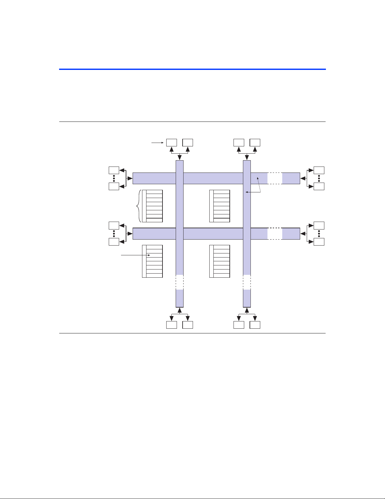
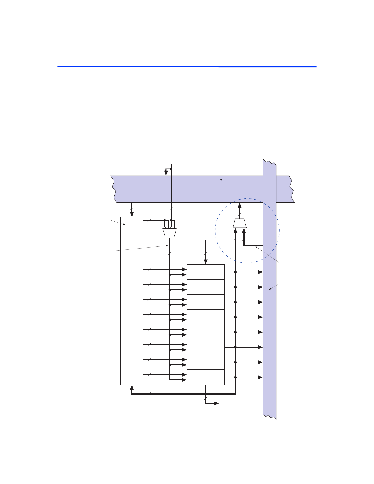
Figure 1 shows a block diagram of the FLEX 8000 architecture. Each
group of eight LEs is combined into an LAB; LABs are arranged into rows
and columns. The I/O pins are supported by I/O elements (IOEs) located
at the ends of rows and columns. Each IOE contains a bidirectional I/O
buffer and a flipflop that can be used as either an input or output register.
Figure 1. FLEX 8000 Device Block Diagram
FLEX 8000 Programmable Logic Device Family Data Sheet
I/O Element
(IOE)
IOE
IOE
Logic Array
Block (LAB)
IOE
IOE
Logic
Element (LE)
IOEIOE IOEIOE
IOEIOE IOEIOE
FastTrack
Interconnect
IOE
IOE
IOE
IOE
3
FLEX 8000
Signal interconnections within FLEX 8000 devices and between device
pins are provided by the FastTrack Interconnect, a series of fast,
continuous channels that run the entire length and width of the device.
IOEs are located at the end of each row (horizontal) and column (vertical)
FastTrack Interconnect path.
Altera Corporation 5
Page 6
FLEX 8000 Programmable Logic Device Family Data Sheet
Logic Array Block
A logic array block (LAB) consists of eight LEs, their associated carry and
cascade chains, LAB control signals, and the LAB local interconnect. The
LAB provides the coarse-grained structure of the FLEX 8000 architecture.
This structure enables FLEX 8000 devices to provide efficient routing,
high device utilization, and high performance. Figure 2 shows a block
diagram of the FLEX 8000 LAB.
Figure 2. FLEX 8000 Logic Array Block
Dedicated
Inputs
Row Interconnect
LAB Local
Interconnect
(32 channels)
LAB Control
Signals
24
4
4
4
Carry-In and
Cascade-In
from LAB
on Left
2
8
See Figure 8
for details.
8
16
Column-to-Row
4
4
4
4
4
4
4
4
LE1
LE2
LE3
LE4
LE5
LE6
LE7
LE8
Interconnect
Column
Interconnect
8
2
Carry-Out and
Cascade-Out
to LAB on Right
6 Altera Corporation
Page 7
FLEX 8000 Programmable Logic Device Family Data Sheet
Each LAB provides four control signals that can be used in all eight LEs.
Two of these signals can be used as clocks, and the other two for
clear/preset control. The LAB control signals can be driven directly from
a dedicated input pin, an I/O pin, or any internal signal via the LAB local
interconnect. The dedicated inputs are typically used for global clock,
clear, or preset signals because they provide synchronous control with
very low skew across the device. FLEX 8000 devices support up to four
individual global clock, clear, or preset control signals. If logic is required
on a control signal, it can be generated in one or more LEs in any LAB and
driven into the local interconnect of the target LAB. This process is called
programmable inversion, and is available for all four LAB control signals.
Logic Element
Figure 3. FLEX 8000 LE
DATA1
DATA2
DATA3
DATA4
LABCTRL1
LABCTRL2
LABCTRL3
LABCTRL4
The logic element (LE) is the smallest unit of logic in the FLEX 8000
architecture, with a compact size that provides efficient logic utilization.
Each LE contains a 4-input LUT, a programmable flipflop, a carry chain,
and cascade chain. Figure 3 shows a block diagram of an LE.
Look-Up
T able
(LUT)
Clear/
Preset
Logic
Clock
Select
Carry-In
Carry
Chain
Carry-Out
Cascade-In
Cascade
Chain
Cascade-Out
DFF
PRN
DQ
CLRN
LE-Out
The LUT is a function generator that can quickly compute any function of
four variables. The programmable flipflop in the LE can be configured for
D, T, JK, or SR operation. The clock, clear, and preset control signals on the
flipflop can be driven by dedicated input pins, general-purpose I/O pins,
or any internal logic. For purely combinatorial functions, the flipflop is
bypassed and the output of the LUT goes directly to the output of the LE.
3
FLEX 8000
Altera Corporation 7
Page 8

FLEX 8000 Programmable Logic Device Family Data Sheet
The FLEX 8000 architecture provides two dedicated high-speed data
paths—carry chains and cascade chains—that connect adjacent LEs
without using local interconnect paths. The carry chain supports highspeed counters and adders; the cascade chain implements wide-input
functions with minimum delay. Carry and cascade chains connect all LEs
in an LAB and all LABs in the same row. Heavy use of carry and cascade
chains can reduce routing flexibility. Therefore, the use of carry and
cascade chains should be limited to speed-critical portions of a design.
Carry Chain
The carry chain provides a very fast (less than 1 ns) carry-forward
function between LEs. The carry-in signal from a lower-order bit moves
forward into the higher-order bit via the carry chain, and feeds into both
the LUT and the next portion of the carry chain. This feature allows the
FLEX 8000 architecture to implement high-speed counters and adders of
arbitrary width. The MAX+PLUS II Compiler can create carry chains
automatically during design processing; designers can also insert carry
chain logic manually during design entry.
Figure 4 shows how an n -bit full adder can be implemented in n + 1 LEs
with the carry chain. One portion of the LUT generates the sum of two bits
using the input signals and the carry-in signal; the sum is routed to the
output of the LE. The register is typically bypassed for simple adders, but
can be used for an accumulator function. Another portion of the LUT and
the carry chain logic generate the carry-out signal, which is routed directly
to the carry-in signal of the next-higher-order bit. The final carry-out
signal is routed to another LE, where it can be used as a general-purpose
signal. In addition to mathematical functions, carry chain logic supports
very fast counters and comparators.
8 Altera Corporation
Page 9
FLEX 8000 Programmable Logic Device Family Data Sheet
Figure 4. FLEX 8000 Carry Chain Operation
Carry-In
a1
b1
a2
b2
a
b
LU
Carry
LUT
Carry Chain
Register
LE
Register
LE
s1
s2
3
n
n
LUT
Carry Chain
Register
LE
s
n
FLEX 8000
LUT
Carry Chain
Register
LE
n
+ 1
Carry-Out
Cascade Chain
With the cascade chain, the FLEX 8000 architecture can implement
functions that have a very wide fan-in. Adjacent LUTs can be used to
compute portions of the function in parallel; the cascade chain serially
connects the intermediate values. The cascade chain can use a logical AND
or logical OR (via De Morgan’s inversion) to connect the outputs of
adjacent LEs. Each additional LE provides four more inputs to the
effective width of a function, with a delay as low as 0.6 ns per LE.
Altera Corporation 9
Page 10
FLEX 8000 Programmable Logic Device Family Data Sheet
The MAX+PLUS II Compiler can create cascade chains automatically
during design processing; designers can also insert cascade chain logic
manually during design entry. Cascade chains longer than eight LEs are
automatically implemented by linking LABs together. The last LE of an
LAB cascades to the first LE in the next LAB in the row.
Figure 5 shows how the cascade function can connect adjacent LEs to
form functions with a wide fan-in. These examples show functions of 4 n
variables implemented with n LEs. For a device with an A-2 speed grade,
the LUT delay is approximately 1.6 ns; the cascade chain delay is 0.6 ns.
With the cascade chain, 4.2 ns is needed to decode a 16-bit address.
Figure 5. FLEX 8000 Cascade Chain Operation
AND Cascade Chain OR Cascade Chain
LE1
d[3..0]
d[7..4]
d[(4n-1)..4(n-1)]
LUT
LUT
LUT
LE2
LE
n
d[3..0]
d[7..4]
d[(4n-1)..4(n-1)]
LE Operating Modes
The FLEX 8000 LE can operate in one of four modes, each of which uses
LE resources differently. See Figure 6. In each mode, seven of the ten
available inputs to the LE—the four data inputs from the LAB local
interconnect, the feedback from the programmable register, and the
carry-in and cascade-in from the previous LE—are directed to different
destinations to implement the desired logic function. The three remaining
inputs to the LE provide clock, clear, and preset control for the register.
The MAX+PLUS II software automatically chooses the appropriate mode
for each application. Design performance can also be enhanced by
designing for the operating mode that supports the desired application.
LUT
LUT
LUT
LE1
LE2
LE
n
10 Altera Corporation
Page 11
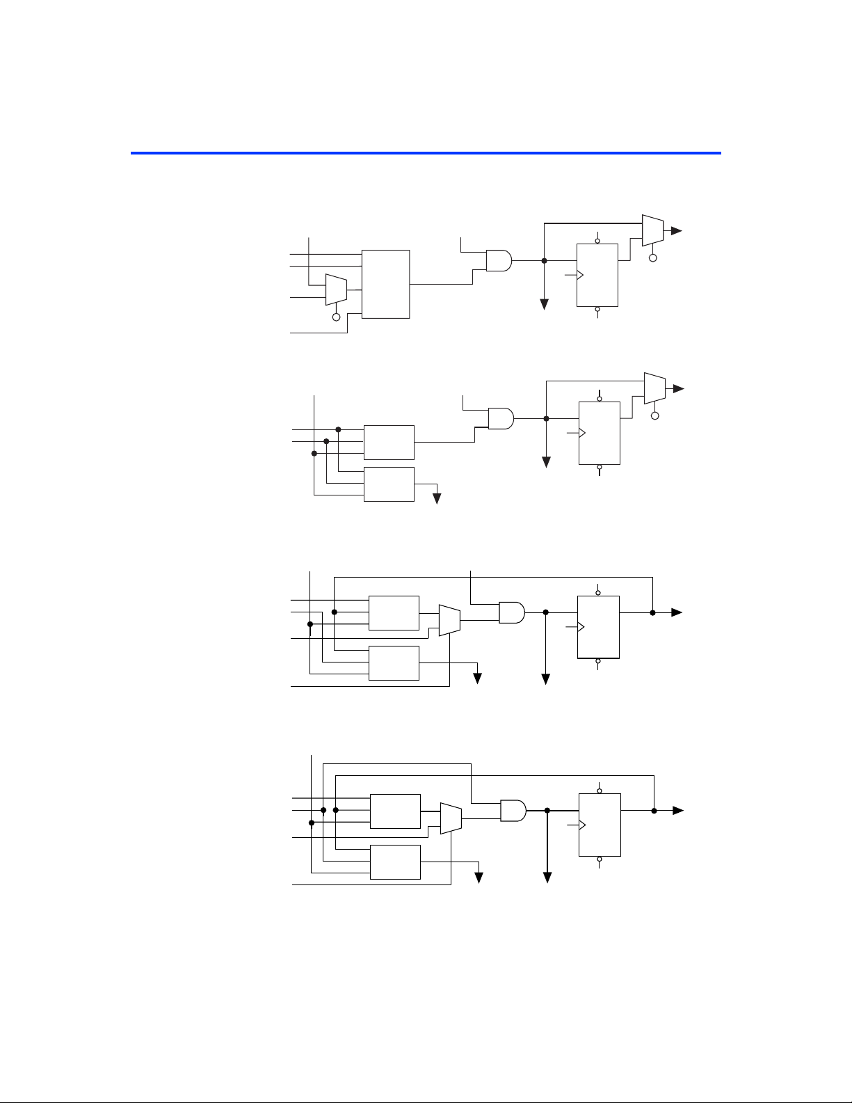
Figure 6. FLEX 8000 LE Operating Modes
Normal Mode
FLEX 8000 Programmable Logic Device Family Data Sheet
Arithmetic Mode
Up/Down
DATA1
DATA2
DATA3
DATA4
DATA1
DATA2
DATA1 (ena)
DATA2 (nclr)
DATA3 (data)
DATA4 (nload)
Carry-In
Carry-In
Carry-In
4-Input
LUT
3-Input
LUT
3-Input
LUT
3-Input
LUT
3-Input
LUT
Cascade-In
Cascade-In
Carry-Out
1
0
Cascade-In
Carry-Out
Cascade-Out
Cascade-Out
Cascade-Out
PRN
DQ
CLRN
PRN
DQ
CLRN
PRN
DQ
CLRN
LE-Out
LE-Out
3
FLEX 8000
LE-Out
Clearable Counter Mode
Carry-In
DATA1 (ena)
DATA2 (nclr)
DATA3 (data)
DATA4 (nload)
3-Input
LUT
3-Input
LUT
1
0
Carry-Out
Cascade-Out
PRN
DQ
CLRN
LE-Out
Altera Corporation 11
Page 12

FLEX 8000 Programmable Logic Device Family Data Sheet
Normal Mode
The normal mode is suitable for general logic applications and wide
decoding functions that can take advantage of a cascade chain. In normal
mode, four data inputs from the LAB local interconnect and the carry-in
signal are the inputs to a 4-input LUT. Using a configurable SRAM bit, the
MAX+PLUS II Compiler automatically selects the carry-in or the DATA3
signal as an input. The LUT output can be combined with the cascade-in
signal to form a cascade chain through the cascade-out signal. The LE-Out
signal—the data output of the LE—is either the combinatorial output of
the LUT and cascade chain, or the data output ( Q) of the programmable
register.
Arithmetic Mode
The arithmetic mode offers two 3-input LUTs that are ideal for
implementing adders, accumulators, and comparators. One LUT
provides a 3-bit function; the other generates a carry bit. As shown in
Figure 6, the first LUT uses the carry-in signal and two data inputs from
the LAB local interconnect to generate a combinatorial or registered
output. For example, in an adder, this output is the sum of three bits: a , b ,
and the carry-in. The second LUT uses the same three signals to generate
a carry-out signal, thereby creating a carry chain. The arithmetic mode
also supports a cascade chain.
Up/Down Counter Mode
The up/down counter mode offers counter enable, synchronous
up/down control, and data loading options. These control signals are
generated by the data inputs from the LAB local interconnect, the carry-in
signal, and output feedback from the programmable register. Two 3-input
LUTs are used: one generates the counter data, and the other generates the
fast carry bit. A 2-to-1 multiplexer provides synchronous loading. Data
can also be loaded asynchronously with the clear and preset register
control signals, without using the LUT resources.
Clearable Counter Mode
The clearable counter mode is similar to the up/down counter mode, but
supports a synchronous clear instead of the up/down control; the clear
function is substituted for the cascade-in signal in the up/down counter
mode. Two 3-input LUTs are used: one generates the counter data, and
the other generates the fast carry bit. Synchronous loading is provided by
a 2-to-1 multiplexer, and the output of this multiplexer is AND ed with a
synchronous clear.
12 Altera Corporation
Page 13

FLEX 8000 Programmable Logic Device Family Data Sheet
Internal Tri-State Emulation
Internal tri-state emulation provides internal tri-stating without the
limitations of a physical tri-state bus. In a physical tri-state bus, the
tri-state buffers’ output enable signals select the signal that drives the bus.
However, if multiple output enable signals are active, contending signals
can be driven onto the bus. Conversely, if no output enable signals are
active, the bus will float. Internal tri-state emulation resolves contending
tri-state buffers to a low value and floating buses to a high value, thereby
eliminating these problems. The MAX+PLUS II software automatically
implements tri-state bus functionality with a multiplexer.
Clear & Preset Logic Control
Logic for the programmable register’s clear and preset functions is
controlled by the DATA3 , LABCTRL1 , and LABCTRL2 inputs to the LE. The
clear and preset control structure of the LE is used to asynchronously load
signals into a register. The register can be set up so that LABCTRL1
implements an asynchronous load. The data to be loaded is driven to
DATA3 ; when LABCTRL1 is asserted, DATA3 is loaded into the register.
During compilation, the MAX+PLUS II Compiler automatically selects
the best control signal implementation. Because the clear and preset
functions are active-low, the Compiler automatically assigns a logic high
to an unused clear or preset.
The clear and preset logic is implemented in one of the following six
asynchronous modes, which are chosen during design entry. LPM
functions that use registers will automatically use the correct
asynchronous mode. See Figure 7.
Clear only
■
Preset only
■
Clear and preset
■
Load with clear
■
Load with preset
■
Load without clear or preset
■
3
FLEX 8000
Altera Corporation 13
Page 14

FLEX 8000 Programmable Logic Device Family Data Sheet
Figure 7. FLEX 8000 LE Asynchronous Clear & Preset Modes
Asynchronous Clear
VCC
PRN
Q
D
CLRN
LABCTRL1 or
LABCTRL2
Asynchronous Load with Clear
LABCTRL1
(Asynchronous
Load)
DATA3
(Data)
LABCTRL2
(Clear)
NOT
NOT
Asynchronous Load with Preset
LABCTRL1
(Asynchronous
Load)
NOT
Asynchronous Preset
LABCTRL1 or
LABCTRL2
D
D
PRN
CLRN
PRN
CLRN
Q
Asynchronous Clear & Preset
LABCTRL1
PRN
Q
Q
LABCTRL2
D
CLRN
LABCTRL2
(Preset)
DATA3
(Data)
NOT
D
PRN
CLRN
Q
Asynchronous Load without Clear or Preset
LABCTRL1
(Asynchronous
Load)
DATA3
(Data)
NOT
NOT
PRN
D
CLRN
Q
14 Altera Corporation
Page 15

FLEX 8000 Programmable Logic Device Family Data Sheet
Asynchronous Clear
A register is cleared by one of the two LABCTRL signals. When the CLRn
port receives a low signal, the register is set to zero.
Asynchronous Preset
An asynchronous preset is implemented as either an asynchronous load
or an asynchronous clear. If DATA3 is tied to VCC, asserting LABCTRLl
asynchronously loads a 1 into the register. Alternatively, the
MAX+PLUS II software can provide preset control by using the clear and
inverting the input and output of the register. Inversion control is
available for the inputs to both LEs and IOEs. Therefore, if a register is
preset by only one of the two LABCTRL signals, the DATA3 input is not
needed and can be used for one of the LE operating modes.
Asynchronous Clear & Preset
When implementing asynchronous clear and preset, LABCTRL1 controls
the preset and LABCTRL2 controls the clear. The DATA3 input is tied to VCC;
therefore, asserting LABCTRL1 asynchronously loads a 1 into the register,
effectively presetting the register. Asserting LABCTRL2 clears the register.
Asynchronous Load with Clear
3
FLEX 8000
When implementing an asynchronous load with the clear, LABCTRL1
implements the asynchronous load of DATA3 by controlling the register
preset and clear. LABCTRL2 implements the clear by controlling the
register clear.
Asynchronous Load with Preset
When implementing an asynchronous load in conjunction with a preset,
the MAX+PLUS II software provides preset control by using the clear and
inverting the input and output of the register. Asserting LABCTRL2 clears
the register, while asserting LABCTRL1 loads the register. The
MAX+PLUS II software inverts the signal that drives the DATA3 signal to
account for the inversion of the register’s output.
Asynchronous Load without Clear or Preset
When implementing an asynchronous load without the clear or preset,
LABCTRL1 implements the asynchronous load of DATA3 by controlling the
register preset and clear.
Altera Corporation 15
Page 16
FLEX 8000 Programmable Logic Device Family Data Sheet
FastTrack Interconnect
In the FLEX 8000 architecture, connections between LEs and device I/O
pins are provided by the FastTrack Interconnect, a series of continuous
horizontal (row) and vertical (column) routing channels that traverse the
entire FLEX 8000 device. This device-wide routing structure provides
predictable performance even in complex designs. In contrast, the
segmented routing structure in FPGAs requires switch matrices to
connect a variable number of routing paths, which increases the delays
between logic resources and reduces performance.
The LABs within FLEX 8000 devices are arranged into a matrix of
columns and rows. Each row of LABs has a dedicated row interconnect
that routes signals both into and out of the LABs in the row. The row
interconnect can then drive I/O pins or feed other LABs in the device.
Figure 8 shows how an LE drives the row and column interconnect.
Figure 8. FLEX 8000 LAB Connections to Row & Column Interconnect
16 Column
Channels
Row Channels
Note (1)
Each LE drives one
row channel.
LE1
LE2
to Local
Feedback
Note:
(1) See Table 4 for the number of row channels.
16 Altera Corporation
to Local
Feedback
Each LE drives up to
two column channels.
Page 17

FLEX 8000 Programmable Logic Device Family Data Sheet
Each LE in an LAB can drive up to two separate column interconnect
channels. Therefore, all 16 available column channels can be driven by the
LAB. The column channels run vertically across the entire device, and
share access to LABs in the same column but in different rows. The
MAX+PLUS II Compiler chooses which LEs must be connected to a
column channel. A row interconnect channel can be fed by the output of
the LE or by two column channels. These three signals feed a multiplexer
that connects to a specific row channel. Each LE is connected to one 3-to-1
multiplexer. In an LAB, the multiplexers provide all 16 column channels
with access to 8 row channels.
Each column of LABs has a dedicated column interconnect that routes
signals out of the LABs into the column. The column interconnect can then
drive I/O pins or feed into the row interconnect to route the signals to
other LABs in the device. A signal from the column interconnect, which
can be either the output of an LE or an input from an I/O pin, must
transfer to the row interconnect before it can enter an LAB. Table 4
summarizes the FastTrack Interconnect resources available in each
FLEX 8000 device.
Table 4. FLEX 8000 FastTrack Interconnect Resources
Device Rows Channels per Row Columns Channels per Column
EPF8282A
EPF8282AV
EPF8452A 2 168 21 16
EPF8636A 3 168 21 16
EPF8820A 4 168 21 16
EPF81188A 6 168 21 16
EPF81500A 6 216 27 16
2 168 13 16
3
FLEX 8000
Figure 9 shows the interconnection of four adjacent LABs, with row,
column, and local interconnects, as well as the associated cascade and
carry chains.
Altera Corporation 17
Page 18
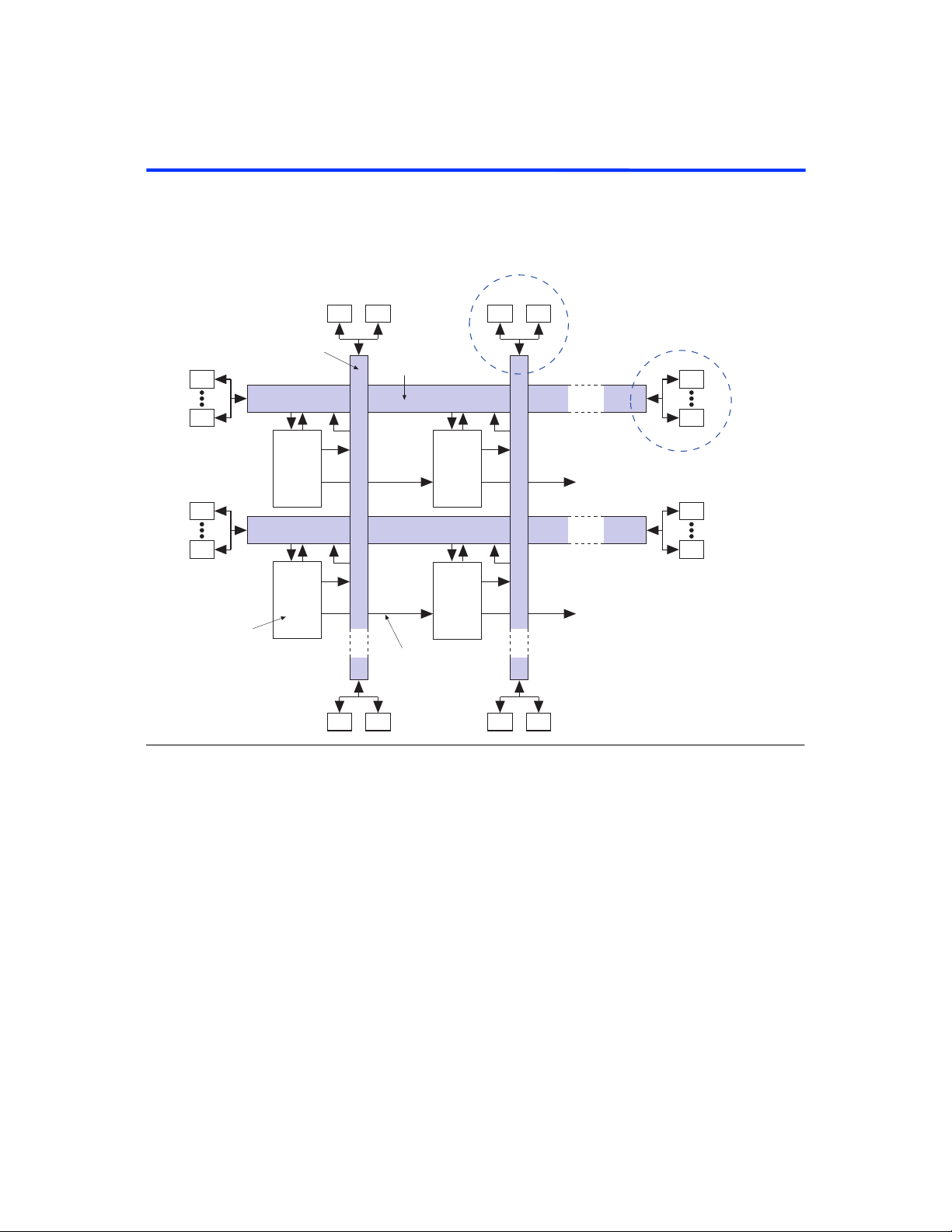
FLEX 8000 Programmable Logic Device Family Data Sheet
Figure 9. FLEX 8000 Device Interconnect Resources
Each LAB is named according to its physical row (A, B, C, etc.) and column (1, 2, 3, etc.) position within the device.
See Figure 11
for details.
IOE
1
IOE
8
IOE
1
IOE
8
LAB Local
Interconnect
Column
Interconnect
LAB
A1
LAB
B1
IOEIOE
Row
Interconnect
LAB
A2
LAB
B2
Cascade &
Carry Chain
IOEIOE IOEIOE
IOEIOE
See Figure 10
for details.
IOE
1
IOE
8
IOE
1
IOE
8
I/O Element
An IOE contains a bidirectional I/O buffer and a register that can be used
either as an input register for external data that requires a fast setup time,
or as an output register for data that requires fast clock-to-output
performance. IOEs can be used as input, output, or bidirectional pins. The
MAX+PLUS II Compiler uses the programmable inversion option to
automatically invert signals from the row and column interconnect where
appropriate. Figure 10 shows the IOE block diagram.
18 Altera Corporation
Page 19
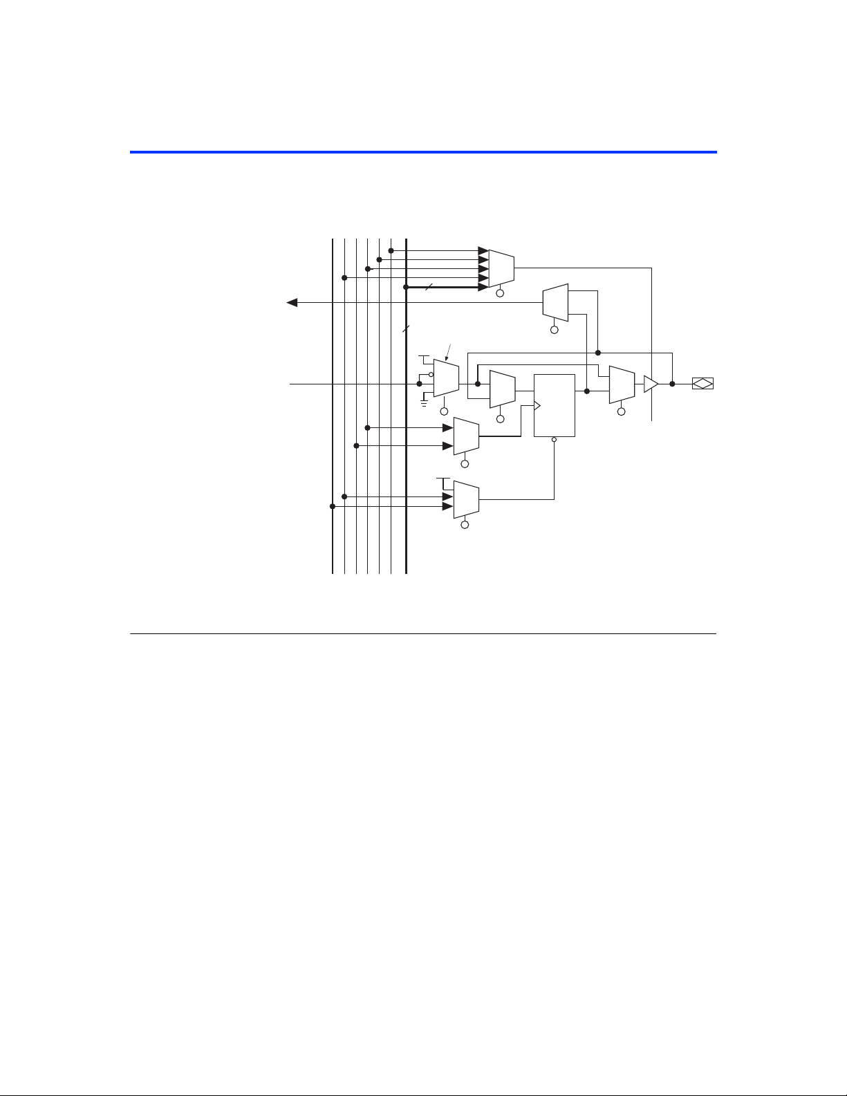
Figure 10. FLEX 8000 IOE
Numbers in parentheses are for EPF81500A devices only.
I/O Controls
FLEX 8000 Programmable Logic Device Family Data Sheet
to Row or Column
Interconnect
from Row or Column
Interconnect
6
Programmable
(6)
Inversion
VCC
DQ
Slew-Rate
Control
CLR0
CLR1/OE0
CLK0
CLK1/OE1
OE2
CLRN
VCC
OE3
(OE [4..9])
Row-to-IOE Connections
Figure 11 illustrates the connection between row interconnect channels
and IOEs. An input signal from an IOE can drive two separate row
channels. When an IOE is used as an output, the signal is driven by an
n-to-1 multiplexer that selects the row channels. The size of the
multiplexer varies with the number of columns in a device. EPF81500A
devices use a 27-to-1 multiplexer; EPF81188A, EPF8820A, EPF8636A, and
EPF8452A devices use a 21-to-1 multiplexer; and EPF8282A and
EPF8282AV devices use a 13-to-1 multiplexer. Eight IOEs are connected to
each side of the row channels.
3
FLEX 8000
Altera Corporation 19
Page 20

FLEX 8000 Programmable Logic Device Family Data Sheet
Figure 11. FLEX 8000 Row-to-IOE Connections
Numbers in parentheses are for EPF81500A devices. See Note (1).
2
2
2
2
Each IOE can drive
up to two row
channels.
Row Interconnect
Each IOE is
driven by an
n-to-1
multiplexer.
168
(216)
22
2
2
2
2
2
2
168
(216)
n
n
n
n
n
n
n
n
2
2
2
2
IOE 1
IOE 2
IOE 3
IOE 4
IOE 5
IOE 6
IOE 7
IOE 8
Note:
(1) n = 13 for EPF8282A and EPF8282AV devices.
n = 21 for EPF8452A, EPF8636A, EPF8820A, and EPF81188A devices.
n = 27 for EPF81500A devices.
Column-to-IOE Connections
Two IOEs are located at the top and bottom of the column channels (see
Figure 12). When an IOE is used as an input, it can drive up to two
separate column channels. The output signal to an IOE can choose from 8
of the 16 column channels through an 8-to-1 multiplexer.
20 Altera Corporation
Page 21

FLEX 8000 Programmable Logic Device Family Data Sheet
Figure 12. FLEX 8000 Column-to-IOE Connections
Each IOE is
driven by an
8-to-1
multiplexer.
IOE
8
Column Interconnect
IOE
8
16
Each IOE can drive
up to two column
signals.
In addition to general-purpose I/O pins, FLEX 8000 devices have four
dedicated input pins. These dedicated inputs provide low-skew, devicewide signal distribution, and are typically used for global clock, clear, and
preset control signals. The signals from the dedicated inputs are available
as control signals for all LABs and I/O elements in the device. The
dedicated inputs can also be used as general-purpose data inputs because
they can feed the local interconnect of each LAB in the device.
3
FLEX 8000
Signals enter the FLEX 8000 device either from the I/O pins that provide
general-purpose input capability or from the four dedicated inputs. The
IOEs are located at the ends of the row and column interconnect channels.
I/O pins can be used as input, output, or bidirectional pins. Each I/O pin
has a register that can be used either as an input register for external data
that requires fast setup times, or as an output register for data that
requires fast clock-to-output performance. The MAX+PLUS II Compiler
uses the programmable inversion option to automatically invert signals
from the row and column interconnect when appropriate.
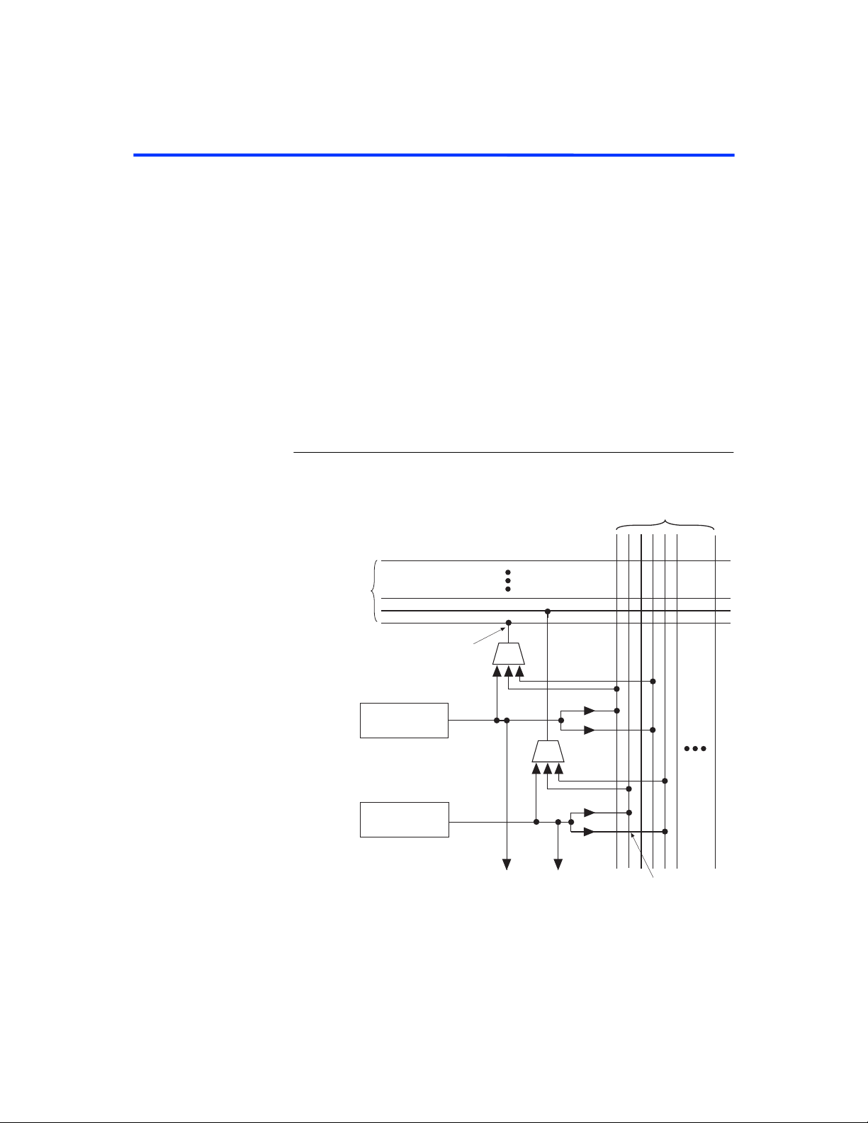
The clock, clear, and output enable controls for the IOEs are provided by
a network of I/O control signals. These signals can be supplied by either
the dedicated input pins or by internal logic. The IOE control-signal paths
are designed to minimize the skew across the device. All control-signal
sources are buffered onto high-speed drivers that drive the signals around
the periphery of the device. This “peripheral bus” can be configured to
provide up to four output enable signals (10 in EPF81500A devices), and
up to two clock or clear signals. Figure 13 shows how two output enable
signals are shared with one clock and one clear signal.
Altera Corporation 21
Page 22

FLEX 8000 Programmable Logic Device Family Data Sheet
The signals for the peripheral bus can be generated by any of the four
dedicated inputs or signals on the row interconnect channels, as shown in
Figure 13. The number of row channels in a row that can drive the
peripheral bus correlates to the number of columns in the FLEX 8000
device. EPF8282A and EPF8282AV devices use 13 channels; EPF8452A,
EPF8636A, EPF8820A, and EPF81188A devices use 21 channels; and
EPF81500A devices use 27 channels. The first LE in each LAB is the source
of the row channel signal. The six peripheral control signals (12 in
EPF81500A devices) can be accessed by each IOE.
Figure 13. FLEX 8000 Peripheral Bus
Numbers in parentheses are for EPF81500A devices.
Programmable
Inversion
Peripheral Control
Signals
Dedicated
Inputs
Row Channels
1
n
Note (1)
4
2
Note:
(1) n = 13 for EPF8282A and EPF8282AV devices.
n = 21 for EPF8452A, EPF8636A, EPF8820A, and EPF81188A devices.
n = 27 for EPF81500A devices.
CLR0
CLR1/OE0
CLK0
CLK1/OE1
OE2
OE3
(OE[4..9])
22 Altera Corporation
Page 23

FLEX 8000 Programmable Logic Device Family Data Sheet
Table 5 lists the source of the peripheral control signal for each FLEX 8000
device by row.
Table 5. Row Sources of FLEX 8000 Peripheral Control Signals
Peripheral
Control Signal
CLK0 Row A Row A Row A Row A Row E Row E
CLK1/OE1 Row B Row B Row C Row C Row B Row B
CLR0 Row A Row A Row B Row B Row F Row F
CLR1/OE0 Row B Row B Row C Row D Row C Row C
OE2 Row A Row A Row A Row A Row D Row A
OE3 Row B Row B Row B Row B Row A Row A
OE4 –––––Row B
OE5 –––––Row C
OE6 –––––Row D
OE7 –––––Row D
OE8 –––––Row E
OE9 –––––Row F
Output
EPF8282A
EPF8282AV
EPF8452A EPF8636A EPF8820A EPF81188A EPF81500A
This section discusses slew-rate control and MultiVolt I/O interface
operation for FLEX 8000 devices.
Configuration
Slew-Rate Control
The output buffer in each IOE has an adjustable output slew rate that can
be configured for low-noise or high-speed performance. A slow slew rate
reduces system noise by slowing signal transitions, adding a maximum
delay of 3.5 ns. The slow slew-rate setting affects only the falling edge of
a signal. The fast slew rate should be used for speed-critical outputs in
systems that are adequately protected against noise. Designers can specify
the slew rate on a pin-by-pin basis during design entry or assign a default
slew rate to all pins on a global basis.
3
FLEX 8000
f
Altera Corporation 23
For more information on high-speed system design, go to Application
Note 75 (High-Speed Board Designs) in this data book.
Page 24

FLEX 8000 Programmable Logic Device Family Data Sheet
MultiVolt I/O Interface
The FLEX 8000 device architecture supports the MultiVolt I/O interface
feature, which allows EPF81500A, EPF81188A, EPF8820A, and EPF8636A
devices to interface with systems with differing supply voltages. These
devices in all packages—except for EPF8636A devices in 84-pin PLCC
packages—can be set for 3.3-V or 5.0-V I/O pin operation. These devices
have one set of VCC pins for internal operation and input buffers
(VCCINT), and another set for I/O output drivers (VCCIO).
The VCCINT pins must always be connected to a 5.0-V power supply. With
a 5.0-V V
compatible with 3.3-V and 5.0-V inputs.
The VCCIO pins can be connected to either a 3.3-V or 5.0-V power supply,
depending on the output requirements. When the VCCIO pins are
connected to a 5.0-V power supply, the output levels are compatible with
5.0-V systems. When the VCCIO pins are connected to a 3.3-V power
supply, the output high is at 3.3 V and is therefore compatible with 3.3-V
or 5.0-V systems. Devices operating with V
incur a nominally greater timing delay of t
on page 26.
level, input voltages are at TTL levels and are therefore
CCINT
levels lower than 4.75 V
CCIO
instead of t
OD2
OD1
. See Table 7
IEEE 1149.1
(JTAG)
Boundary-Scan
The EPF8282A, EPF8282AV, EPF8636A, EPF8820A, and EPF81500A
devices provide JTAG BST circuitry. FLEX 8000 devices with JTAG
circuitry support the JTAG instructions shown in Table 6. Figure 14
shows the timing requirements for the JTAG signals.
Support
Table 6. EPF8282A, EPF8282AV, EPF8636A, EPF8820A & EPF81500A JTAG Instructions
JTAG Instruction Description
SAMPLE/PRELOAD Allows a snapshot of the signals at the device pins to be captured and examined during
normal device operation, and permits an initial data pattern to be output at the device pins.
EXTEST Allows the external circuitry and board-level interconnections to be tested by forcing a test
pattern at the output pins and capturing test results at the input pins.
BYPASS Places the 1-bit bypass register between the TDI and TDO pins, which allows the BST
data to pass synchronously through the selected device to adjacent devices during
normal device operation.
24 Altera Corporation
Page 25

FLEX 8000 Programmable Logic Device Family Data Sheet
Figure 14. EPF8282A, EPF8282AV, EPF8636A, EPF8820A & EPF81500A JTAG
Waveforms
TMS
TDI
t
JCP
JCH
t
JCL
t
JPSU
t
JPH
t
TCK
t
JPZX
t
JPCO
t
JPXZ
TDO
t
JSH
t
JSCO
t
JSXZ
Signal
to Be
Captured
Signal
to Be
Driven
t
JSZX
t
JSSU
Table 7 shows the timing parameters and values for EPF8282A,
EPF8282AV, EPF8636A, EPF8820A, and EPF81500A devices.
3
FLEX 8000
Altera Corporation 25
Page 26

FLEX 8000 Programmable Logic Device Family Data Sheet
Table 7. JTAG Timing Parameters & Values
f
Symbol Parameter EPF8282A
Unit
EPF8282AV
EPF8636A
EPF8820A
EPF81500A
Min Max
t
JCP
t
JCH
t
JCL
t
JPSU
t
JPH
t
JPCO
t
JPZX
t
JPXZ
t
JSSU
t
JSH
t
JSCO
t
JSZX
t
JSXZ
TCK clock period 100 ns
TCK clock high time 50 ns
TCK clock low time 50 ns
JTAG port setup time 20 ns
JTAG port hold time 45 ns
JTAG port clock to output 25 ns
JTAG port high-impedance to valid output 25 ns
JTAG port valid output to high-impedance 25 ns
Capture register setup time 20 ns
Capture register hold time 45 ns
Update register clock to output 35 ns
Update register high-impedance to valid output 35 ns
Update register valid output to high-impedance 35 ns
For detailed information on JTAG operation in FLEX 8000 devices, refer to
Application Note 39 (JTAG Boundary-Scan Testing in Altera Devices).
Generic Testing
Each FLEX 8000 device is functionally tested and specified by Altera.
Complete testing of each configurable SRAM bit and all logic
functionality ensures 100% configuration yield. AC test measurements for
FLEX 8000 devices are made under conditions equivalent to those shown
in Figure 15. Designers can use multiple test patterns to configure devices
during all stages of the production flow.
26 Altera Corporation
Page 27

FLEX 8000 Programmable Logic Device Family Data Sheet
Figure 15. FLEX 8000 AC Test Conditions
Power supply transients can affect AC
measurements. Simultaneous transitions of
multiple outputs should be avoided for
accurate measurement. Threshold tests
must not be performed under AC
conditions.
Large-amplitude, fast-ground-current
transients normally occur as the device
outputs discharge the load capacitances.
When these transients flow through the
parasitic inductance between the device
ground pin and the test system ground,
significant reductions in observable noise
immunity can result. Numbers in
464 Ω
(703 Ω)
Device
Output
250 Ω
(8.06 KΩ)
Device input
rise and fall
times < 3 ns
VCC
to T est
System
C1 (includes
JIG capacitance)
Operating
Conditions
The following tables provide information on absolute maximum ratings,
recommended operating conditions, operating conditions, and
capacitance for 5.0-V and 3.3-V FLEX 8000 devices.
FLEX 8000 5.0-V Device Absolute Maximum Ratings Note (1)
Symbol Parameter Conditions Min Max Unit
V
V
I
T
T
T
OUT
Supply voltage With respect to ground,
CC
DC input voltage –2.0 7.0 V
I
DC output current, per pin –25 25 mA
Storage temperature No bias –65 150 ° C
STG
Ambient temperature Under bias –65 135 ° C
AMB
Junction temperature Ceramic packages, under bias 150 ° C
J
PQFP and RQFP, under bias 135 ° C
Note (2)
–2.0 7.0 V
FLEX 8000 5.0-V Device Recommended Operating Conditions
Symbol Parameter Conditions Min Max Unit
V
V
V
V
T
t
R
t
F
Supply voltage for internal logic and
CCINT
input buffers
Supply voltage for output buffers,
CCIO
5.0-V operation
Supply voltage for output buffers,
3.3-V operation
Input voltage 0 V
I
Output voltage 0 V
O
Operating temperature For commercial use 0 70 ° C
A
Input rise time 40 ns
Input fall time 40 ns
Notes (3), (4)
Notes (3), (4)
Notes (3), (4)
For industrial use –40 85 ° C
4.75 (4.50) 5.25 (5.50) V
4.75 (4.50) 5.25 (5.50) V
3.00 (3.00) 3.60 (3.60) V
CCINT
CCIO
3
FLEX 8000
V
V
Altera Corporation 27
Page 28

FLEX 8000 Programmable Logic Device Family Data Sheet
FLEX 8000 5.0-V Device DC Operating Conditions Notes (5), (6)
Symbol Parameter Conditions Min Typ Max Unit
V
V
V
V
I
I
I
I
OZ
CC0
High-level input voltage 2.0 V
IH
Low-level input voltage –0.3 0.8 V
IL
5.0-V high-level TTL output
OH
voltage
3.3-V high-level TTL output
voltage
3.3-V high-level CMOS output
voltage
5.0-V low-level TTL output voltage IOL = 12 mA DC,
OL
3.3-V low-level TTL output voltage I
3.3-V low-level CMOS output
voltage
IOH = –4 mA DC,
V
= 4.75 V
CCIO
I
= –4 mA DC,
OH
V
= 3.00 V
CCIO
I
= –0.1 mA DC,
OH
V
= 3.00 V
CCIO
V
= 4.75 V
CCIO
= 12 mA DC,
OL
V
= 3.00 V
CCIO
I
= 0.1 mA DC,
OL
V
= 3.00 V
CCIO
Note (7)
Note (7)
Note (7)
Note (7)
Note (7)
Note (7)
2.4 V
2.4 V
V
– 0.2 V
CCIO
Input leakage current VI = VCC or ground –10 10 µA
Tri-state output off-state current VO = VCC or ground –40 40 µA
VCC supply current (standby) VI = ground, no load 0.5 10 mA
+
CCINT
0.3
0.45 V
0.45 V
0.2 V
FLEX 8000 5.0-V Device Capacitance Note (8)
V
Symbol Parameter Conditions Min Max Unit
C
C
28 Altera Corporation
Input capacitance VIN = 0 V, f = 1.0 MHz 10 pF
IN
Output capacitance V
OUT
= 0 V, f = 1.0 MHz 10 pF
OUT
Page 29

FLEX 8000 Programmable Logic Device Family Data Sheet
Notes to tables:
(1) See the Operating Requirements for Altera Devices Data Sheet in this data book.
(2) Minimum DC input is –0.3 V. During transitions, the inputs may undershoot to –2.0 V or overshoot to 7.0 V for
periods shorter than 20 ns under no-load conditions.
(3) The maximum V
(4) Numbers in parentheses are for industrial-temperature-range devices.
(5) Typical values are for T
(6) These values are specified under “FLEX 8000 5.0-V Device Recommended Operating Conditions” on page 27.
(7) The I
parameter refers to high-level TTL or CMOS output current; the IOL parameter refers to low-level TTL or
OH
CMOS output current.
rise time is 100 ms.
CC
= 25° C and VCC = 5.0 V.
A
(8) Capacitance is sample-tested only.
FLEX 8000 3.3-V Device Absolute Maximum Ratings
Note (1)
Symbol Parameter Conditions Min Max Unit
V
V
I
T
T
T
OUT
Supply voltage With respect to ground,
CC
DC input voltage –2.0 5.3 V
I
DC output current, per pin –25 25 mA
Storage temperature No bias –65 150 ° C
STG
Ambient temperature Under bias –65 135 ° C
AMB
Junction temperature Plastic packages, under bias 135 ° C
J
Note (2)
–2.0 5.3 V
FLEX 8000 3.3-V Device Recommended Operating Conditions
Symbol Parameter Conditions Min Max Unit
V
V
V
T
t
R
t
F
Supply voltage
CC
Input voltage 0VCCV
I
Output voltage 0VCCV
O
Operating temperature For commercial use 0 70 ° C
A
Input rise time 40 ns
Input fall time 40 ns
Note (3)
3.0 3.6 V
FLEX 8000 3.3-V Device DC Operating Conditions Note (4)
Symbol Parameter Conditions Min Typ Max Unit
V
V
V
V
I
I
I
I
OZ
CC0
High-level input voltage 2.0 VCC + 0.3 V
IH
Low-level input voltage –0.3 0.8 V
IL
High-level output voltage IOH = –0.1 mA DC,
OH
Low-level output voltage IOL = 4 mA DC,
OL
Input leakage current VI = VCC or ground –10 10 µA
Tri-state output off-state current VO = VCC or ground –40 40 µA
VCC supply current (standby) VI = ground, no load,
Note (5)
Note (5)
Note (6)
VCC – 0.2 V
0.3 10 mA
0.45 V
3
FLEX 8000
Altera Corporation 29
Page 30

FLEX 8000 Programmable Logic Device Family Data Sheet
e
FLEX 8000 3.3-V Device Capacitance Note (7)
Symbol Parameter Conditions Min Max Unit
C
C
Notes to tables:
(1) See the Operating Requirements for Altera Devices Data Sheet in this data book.
(2) Minimum DC input is –0.3 V. During transitions, the inputs may undershoot to –2.0 V or overshoot to 5.3 V for
(3) The maximum V
(4) These values are specified under “FLEX 8000 3.3-V Device Recommended Operating Conditions” on page 29.
(5) The I
(6) Typical values are for T
(7) Capacitance is sample-tested only.
Input capacitance VIN = 0 V, f = 1.0 MHz 10 pF
IN
Output capacitance V
OUT
= 0 V, f = 1.0 MHz 10 pF
OUT
periods shorter than 20 ns under no-load conditions.
rise time is 100 ms. VCC must rise monotonically.
CC
parameter refers to high-level TTL output current; the IOL parameter refers to low-level TTL output current.
OH
= 25° C and VCC = 3.3 V.
A
Figures 16 and 17 show the typical output drive characteristics of 5.0-V
FLEX 8000 devices. The output driver is compliant with the PCI Local Bus
Specification, Revision 2.1.
Figure 16. Output Drive Characteristics of 5.0-V FLEX 8000 Devices (except EPF8282A)
200
200
Output Current (mA) Typ.
O
I
150
100
I
OL
V
= 5.0 V
CCINT
V
= 5.0 V
CCIO
150
100
Room T emperature
I
50
12345
OH
50
Output Current (mA) Typ.
O
I
VO Output Voltage (V)
I
OL
V
= 5.0 V
CCINT
V
= 3.3 V
CCIO
Room Temperatur
I
OH
1234
VO Output Voltage (V)
30 Altera Corporation
Page 31

FLEX 8000 Programmable Logic Device Family Data Sheet
Figure 17. Output Drive Characteristics of EPF8282A Devices with 5.0-V V
150
120
I
OL
CCIO
VCC = 5.0 V
Room Temperature
90
I
OH
Output Current (mA) Typ.
O
I
60
30
12345
VO Output Voltage (V)
Figure 18 shows the typical output drive characteristics of EPF8282AV
devices.
Figure 18. Output Drive Characteristics of EPF8282AV Devices
100
3
FLEX 8000
I
75
50
OL
VCC = 3.3 V
Room Temperature
I
OH
Output Current (mA) Typ.
O
I
25
1234
VO Output Voltage (V)
Altera Corporation 31
Page 32

FLEX 8000 Programmable Logic Device Family Data Sheet
Timing Model
The continuous, high-performance FastTrack Interconnect routing
structure ensures predictable performance and accurate simulation and
timing analysis. This predictable performance contrasts with that of
FPGAs, which use a segmented connection scheme and hence have
unpredictable performance. Timing simulation and delay prediction are
available with the MAX+PLUS II Simulator and Timing Analyzer, or with
industry-standard EDA tools. The Simulator offers both pre-synthesis
functional simulation to evaluate logic design accuracy and postsynthesis timing simulation with 0.1-ns resolution. The Timing Analyzer
provides point-to-point timing delay information, setup and hold time
prediction, and device-wide performance analysis.
Tables 8 through 11 describe the FLEX 8000 timing parameters and their
symbols.
Table 8. FLEX 8000 Internal Timing Parameters Note (1)
Symbol Parameter
t
IOD
t
IOC
t
IOE
t
IOCO
t
IOCOMB
t
IOSU
t
IOH
t
IOCLR
t
IN
t
OD1
t
OD2
t
OD3
t
XZ
t
ZX1
t
ZX2
t
ZX3
IOE register data delay
IOE register control signal delay
Output enable delay
IOE register clock-to-output delay
IOE combinatorial delay
IOE register setup time before clock; IOE register recovery time after asynchronous clear
IOE register hold time after clock
IOE register clear delay
Input pad and buffer delay
Output buffer and pad delay, slow slew rate = off, V
Output buffer and pad delay, slow slew rate = off, V
Output buffer and pad delay, slow slew rate = on, C1 = 35 pF,
Output buffer disable delay, C1 = 5 pF
Output buffer enable delay, slow slew rate = off, V
Output buffer enable delay, slow slew rate = off, V
CCIO
CCIO
Output buffer enable delay, slow slew rate = on, C1 = 35 pF,
= 5.0 V, C1 = 35 pF,
CCIO
= 3.3 V, C1 = 35 pF,
CCIO
Note (3)
= 5.0 V, C1 = 35 pF,
= 3.3 V, C1 = 35 pF,
Note (3)
Note (2)
Note (2)
Note (2)
Note (2)
32 Altera Corporation
Page 33

FLEX 8000 Programmable Logic Device Family Data Sheet
Table 9. FLEX 8000 LE Timing Parameters Note (1)
Symbol Parameter
t
LUT
t
CLUT
t
RLUT
t
GATE
t
CASC
t
CICO
t
CGEN
t
CGENR
t
C
t
CH
t
CL
t
CO
t
COMB
t
SU
t
H
t
PRE
t
CLR
LUT delay for data-in
LUT delay for carry-in
LUT delay for LE register feedback
Cascade gate delay
Cascade chain routing delay
Carry-in to carry-out delay
Data-in to carry-out delay
LE register feedback to carry-out delay
LE register control signal delay
LE register clock high time
LE register clock low time
LE register clock-to-output delay
Combinatorial delay
LE register setup time before clock; LE register recovery time after asynchronous preset, clear, or load
LE register hold time after clock
LE register preset delay
LE register clear delay
3
FLEX 8000
Table 10. FLEX 8000 Interconnect Timing Parameters Note (1)
Symbol Parameter
t
LABCASC
t
LABCARRY
t
LOCAL
t
ROW
t
COL
t
DIN_C
t
DIN_D
t
DIN_IO
Cascade delay between LEs in different LABs
Carry delay between LEs in different LABs
LAB local interconnect delay
Row interconnect routing delay,
Note (4)
Column interconnect routing delay
Dedicated input to LE control delay
Dedicated input to LE data delay,
Note (4)
Dedicated input to IOE control delay
Table 11. FLEX 8000 External Reference Timing Characteristics Note (5)
Symbol Parameter
t
DRR
t
ODH
Altera Corporation 33
Register-to-register delay via 4 LEs, 3 row interconnects, and 4 local interconnects,
Output data hold time after clock,
Note (7)
Note (6)
Page 34

FLEX 8000 Programmable Logic Device Family Data Sheet
Notes to tables:
(1) Internal timing parameters cannot be measured explicitly. They are worst-case delays based on testable and
external parameters specified by Altera. Internal timing parameters should be used for estimating device
performance. Post-compilation timing simulation or timing analysis is required to determine actual worst-case
performance.
(2) These values are specified under “FLEX 8000 3.3-V Device Recommended Operating Conditions” on page 29.
(3) For the t
(4) The t
timing analysis is required to determine actual worst-case performance.
(5) External reference timing characteristics are factory-tested, worst-case values specified by Altera. A representative
subset of signal paths is tested to approximate typical device applications.
(6) For more information on test conditions, see Application Note 76 (Understanding FLEX 8000 Timing) in this data book.
(7) This parameter is a guideline that is sample-tested only and is based on extensive device characterization. This
parameter applies to global and non-global clocking, and for LE and I/O element registers.
ROW
OD3
and t
and t
DIN_D
parameters, V
ZX3
delays are worst-case values for typical applications. Post-compilation timing simulation or
= 3.3 V or 5.0 V.
CCIO
The FLEX 8000 timing model shows the delays for various paths and
functions in the circuit. See Figure 19. This model contains three distinct
parts: the LE; the IOE; and the interconnect, including the row and column
FastTrack Interconnect, LAB local interconnect, and carry and cascade
interconnect paths. Each parameter shown in Figure 19 is expressed as a
worst-case value in the “Timing Parameters” tables in this data sheet.
Hand-calculations that use the FLEX 8000 timing model and these timing
parameters can be used to estimate FLEX 8000 device performance.
Timing simulation or timing analysis after compilation is required to
determine the final worst-case performance. Table 12 summarizes the
interconnect paths shown in Figure 19.
f
For more information on timing parameters, go to Application Note 76
(Understanding FLEX 8000 Timing) in this data book.
Table 12. FLEX 8000 Timing Model Interconnect Paths
Source Destination Total Delay
LE-Out LE in same LAB
LE-Out LE in same row, different LAB
LE-Out LE in different row
LE-Out IOE on column
LE-Out IOE on row
IOE on row LE in same row
IOE on column Any LE
34 Altera Corporation
t
LOCAL
t
ROW
t
COL
t
COL
t
ROW
t
ROW
t
COL
+ t
+ t
+ t
+ t
LOCAL
ROW
LOCAL
ROW
+ t
+ t
LOCAL
LOCAL
Page 35

Figure 19. FLEX 8000 Timing Model
I/O Pin
IOE
FLEX 8000 Programmable Logic Device Family Data Sheet
ROW
t
Output
I/O Register
Output Data
LE
Register
Cascade
OD1tOD2tOD3tXZtZX1tZX2tZX3
t
Delays
IOCOtIOCOMBtIOSUtIOHtIOCLR
Delays
t
IOD
t
Delay
LE-Out
tCOt
Delays
GATE
t
Gate Delay
Control
I/O Register
COMBtSUtHtPREtCLR
IOCtIOE
t
COL
t
Input
Delay
IN
t
Data-In
Cascade
Routing Delay
CASC
t
LABCASC
t
Cascade-Out
to Next LE in
Same LAB
Cascade-Out
to Next LE in
Next LAB
3
FLEX 8000
Carry-Out
to Next LE
in Next
Carry-Out
to Next LE
in Same
LAB
LAB
Cascade-In from
Previous LE
Carry-In from
Previous LE
LUT Delay
LABCARRY
t
C
Delay
CGEN
RLUT
LUT
CLUT
t
t
t
t
Carry Chain
LOCAL
t
CGENRtCICO
t
Control
Register
t
DIN_D
DIN_CtDIN_IO
t
t
Dedicated
Input Delays
Altera Corporation 35
Page 36

FLEX 8000 Programmable Logic Device Family Data Sheet
EPF8282A Internal Timing Parameters
EPF8282A I/O Element Timing Parameters
Symbol
A-2 Speed Grade A-3 Speed Grade A-4 Speed Grade
Min Max Min Max Min Max
t
IOD
t
IOC
t
IOE
t
IOCO
t
IOCOMB
t
IOSU
t
IOH
t
IOCLR
t
IN
t
OD1
t
OD2
t
OD3
t
XZ
t
ZX1
t
ZX2
t
ZX3
1.4 1.6 1.8 ns
0.0 0.0 0.0 ns
0.7 0.8 0.9 ns
1.7 1.8 1.9 ns
1.7 1.8 1.9 ns
1.0 1.0 1.0 ns
0.3 0.2 0.1 ns
1.2 1.2 1.2 ns
1.5 1.6 1.7 ns
1.1 1.4 1.7 ns
–––ns
4.6 4.9 5.2 ns
1.4 1.6 1.8 ns
1.4 1.6 1.8 ns
–––ns
4.9 5.1 5.3 ns
Unit
EPF8282A Interconnect Timing Parameters
Symbol
A-2 Speed Grade A-3 Speed Grade A-4 Speed Grade
Unit
Min Max Min Max Min Max
t
LABCASC
t
LABCARRY
t
LOCAL
t
ROW
t
COL
t
DIN_C
t
DIN_D
t
DIN_IO
36 Altera Corporation
0.3 0.3 0.4 ns
0.3 0.3 0.4 ns
0.5 0.6 0.8 ns
4.2 4.2 4.2 ns
2.5 2.5 2.5 ns
5.0 5.0 5.5 ns
7.2 7.2 7.2 ns
5.0 5.0 5.5 ns
Page 37

EPF8282A LE Timing Parameters
Symbol
A-2 Speed Grade A-3 Speed Grade A-4 Speed Grade
Min Max Min Max Min Max
t
LUT
t
CLUT
t
RLUT
t
GATE
t
CASC
t
CICO
t
CGEN
t
CGENR
t
C
t
CH
t
CL
t
CO
t
COMB
t
SU
t
H
t
PRE
t
CLR
4.0 4.0 4.0 ns
4.0 4.0 4.0 ns
0.8 1.1 1.2 ns
0.9 1.1 1.5 ns
FLEX 8000 Programmable Logic Device Family Data Sheet
Unit
2.0 2.5 3.2 ns
0.0 0.0 0.0 ns
0.9 1.1 1.5 ns
0.0 0.0 0.0 ns
0.6 0.7 0.9 ns
0.4 0.5 0.6 ns
0.4 0.5 0.7 ns
0.9 1.1 1.5 ns
1.6 2.0 2.5 ns
0.4 0.5 0.6 ns
0.4 0.5 0.6 ns
3
FLEX 8000
0.6 0.7 0.8 ns
0.6 0.7 0.8 ns
EPF8282A External Timing Parameters
Symbol
A-2 Speed Grade A-3 Speed Grade A-4 Speed Grade
Unit
Min Max Min Max Min Max
t
DRR
t
ODH
1.0 1.0 1.0 ns
Altera Corporation 37
15.8 19.8 24.8 ns
Page 38

FLEX 8000 Programmable Logic Device Family Data Sheet
EPF8282AV Internal Timing Parameters
EPF8282AV I/O Element Timing Parameters
Symbol
A-3 Speed Grade A-4 Speed Grade
Min Max Min Max
t
IOD
t
IOC
t
IOE
t
IOCO
t
IOCOMB
t
IOSU
t
IOH
t
IOCLR
t
IN
t
OD1
t
OD2
t
OD3
t
XZ
t
ZX1
t
ZX2
t
ZX3
1.8 2.8 ns
0.0 0.2 ns
0.9 2.2 ns
1.9 2.0 ns
1.9 2.0 ns
1.0 2.0 ns
0.1 0.0 ns
1.2 2.3 ns
1.7 3.4 ns
1.7 4.1 ns
––ns
5.2 7.1 ns
1.8 4.3 ns
1.8 4.3 ns
––ns
5.3 8.3 ns
EPF8282AV Interconnect Timing Parameters
Unit
Symbol
A-3 Speed Grade A-4 Speed Grade
Unit
Min Max Min Max
t
LABCASC
t
LABCARRY
t
LOCAL
t
ROW
t
COL
t
DIN_C
t
DIN_D
t
DIN_IO
38 Altera Corporation
0.4 1.3 ns
0.4 0.8 ns
0.8 1.5 ns
4.2 6.3 ns
2.5 3.8 ns
5.5 8.0 ns
7.2 10.8 ns
5.5 9.0 ns
Page 39

FLEX 8000 Programmable Logic Device Family Data Sheet
EPF8282AV Logic Element Timing Parameters
Symbol
A-3 Speed Grade A-4 Speed Grade
Min Max Min Max
t
LUT
t
CLUT
t
RLUT
t
GATE
t
CASC
t
CICO
t
CGEN
t
CGENR
t
C
t
CH
t
CL
t
CO
t
COMB
t
SU
t
H
t
PRE
t
CLR
4.0 6.0 ns
4.0 6.0 ns
1.2 2.4 ns
1.5 4.6 ns
3.2 7.3 ns
0.0 1.4 ns
1.5 5.1 ns
0.0 0.0 ns
0.9 2.8 ns
0.6 1.5 ns
0.7 2.2 ns
1.5 3.7 ns
2.5 4.7 ns
0.6 0.9 ns
0.6 0.9 ns
0.8 1.3 ns
0.8 1.3 ns
EPF8282AV External Timing Parameters
Unit
3
FLEX 8000
Symbol
A-3 Speed Grade A-4 Speed Grade
Unit
Min Max Min Max
t
DRR
t
ODH
1.0 1.0 ns
Altera Corporation 39
24.8 50.1 ns
Page 40

FLEX 8000 Programmable Logic Device Family Data Sheet
EPF8452A Internal Timing Parameters
EPF8452A I/O Element Timing Parameters
Symbol
A-2 Speed Grade A-3 Speed Grade A-4 Speed Grade
Min Max Min Max Min Max
t
IOD
t
IOC
t
IOE
t
IOCO
t
IOCOMB
t
IOSU
t
IOH
t
IOCLR
t
IN
t
OD1
t
OD2
t
OD3
t
XZ
t
ZX1
t
ZX2
t
ZX3
1.4 1.6 1.8 ns
0.0 0.0 0.0 ns
0.7 0.8 0.9 ns
1.7 1.8 1.9 ns
1.7 1.8 1.9 ns
1.0 1.0 1.0 ns
0.3 0.2 0.1 ns
1.2 1.2 1.2 ns
1.5 1.6 1.7 ns
1.1 1.4 1.7 ns
–––ns
4.6 4.9 5.2 ns
1.4 1.6 1.8 ns
1.4 1.6 1.8 ns
–––ns
4.9 5.1 5.3 ns
Unit
EPF8452A Interconnect Timing Parameters
Symbol
A-2 Speed Grade A-3 Speed Grade A-4 Speed Grade
Unit
Min Max Min Max Min Max
t
LABCASC
t
LABCARRY
t
LOCAL
t
ROW
t
COL
t
DIN_C
t
DIN_D
t
DIN_IO
40 Altera Corporation
0.3 0.4 0.4 ns
0.3 0.4 0.4 ns
0.5 0.5 0.7 ns
5.0 5.0 5.0 ns
3.0 3.0 3.0 ns
5.0 5.0 5.5 ns
7.0 7.0 7.5 ns
5.0 5.0 5.5 ns
Page 41

EPF8452A LE Timing Parameters
Symbol
A-2 Speed Grade A-3 Speed Grade A-4 Speed Grade
Min Max Min Max Min Max
t
LUT
t
CLUT
t
RLUT
t
GATE
t
CASC
t
CICO
t
CGEN
t
CGENR
t
C
t
CH
t
CL
t
CO
t
COMB
t
SU
t
H
t
PRE
t
CLR
4.0 4.0 4.0 ns
4.0 4.0 4.0 ns
0.8 1.0 1.1 ns
0.9 1.1 1.4 ns
FLEX 8000 Programmable Logic Device Family Data Sheet
Unit
2.0 2.3 3.0 ns
0.0 0.2 0.1 ns
0.9 1.6 1.6 ns
0.0 0.0 0.0 ns
0.6 0.7 0.9 ns
0.4 0.5 0.6 ns
0.4 0.9 0.8 ns
0.9 1.4 1.5 ns
1.6 1.8 2.4 ns
0.4 0.5 0.6 ns
0.4 0.5 0.6 ns
3
FLEX 8000
0.6 0.7 0.8 ns
0.6 0.7 0.8 ns
EPF8452A External Timing Parameters
Symbol
A-2 Speed Grade A-3 Speed Grade A-4 Speed Grade
Unit
Min Max Min Max Min Max
t
DRR
t
ODH
1.0 1.0 1.0 ns
Altera Corporation 41
16.0 20.0 25.0 ns
Page 42

FLEX 8000 Programmable Logic Device Family Data Sheet
EPF8636A Internal Timing Parameters
EPF8636A I/O Element Timing Parameters
Symbol
A-2 Speed Grade A-3 Speed Grade A-4 Speed Grade
Min Max Min Max Min Max
t
IOD
t
IOC
t
IOE
t
IOCO
t
IOCOMB
t
IOSU
t
IOH
t
IOCLR
t
IN
t
OD1
t
OD2
t
OD3
t
XZ
t
ZX1
t
ZX2
t
ZX3
1.4 1.6 1.8 ns
0.0 0.0 0.0 ns
0.7 0.8 0.9 ns
1.7 1.8 1.9 ns
1.7 1.8 1.9 ns
1.0 1.0 1.0 ns
0.3 0.2 0.1 ns
1.2 1.2 1.2 ns
1.5 1.6 1.7 ns
1.1 1.4 1.7 ns
1.6 1.9 2.2 ns
4.6 4.9 5.2 ns
1.4 1.6 1.8 ns
1.4 1.6 1.8 ns
1.9 2.1 2.3 ns
4.9 5.1 5.3 ns
Unit
EPF8636A Interconnect Timing Parameters
Symbol
A-2 Speed Grade
A-3 Speed Grade A-4 Speed Grade
Unit
Min Max Min Max Min Max
t
LABCASC
t
LABCARRY
t
LOCAL
t
ROW
t
COL
t
DIN_C
t
DIN_D
t
DIN_IO
42 Altera Corporation
0.3 0.4 0.4 ns
0.3 0.4 0.4 ns
0.5 0.5 0.7 ns
5.0 5.0 5.0 ns
3.0 3.0 3.0 ns
5.0 5.0 5.5 ns
7.0 7.0 7.5 ns
5.0 5.0 5.5 ns
Page 43

EPF8636A LE Timing Parameters
Symbol
A-2 Speed Grade A-3 Speed Grade A-4 Speed Grade
Min Max Min Max Min Max
t
LUT
t
CLUT
t
RLUT
t
GATE
t
CASC
t
CICO
t
CGEN
t
CGENR
t
C
t
CH
t
CL
t
CO
t
COMB
t
SU
t
H
t
PRE
t
CLR
4.0 4.0 4.0 ns
4.0 4.0 4.0 ns
0.8 1.0 1.1 ns
0.9 1.1 1.4 ns
FLEX 8000 Programmable Logic Device Family Data Sheet
Unit
2.0 2.3 3.0 ns
0.0 0.2 0.1 ns
0.9 1.6 1.6 ns
0.0 0.0 0.0 ns
0.6 0.7 0.9 ns
0.4 0.5 0.6 ns
0.4 0.9 0.8 ns
0.9 1.4 1.5 ns
1.6 1.8 2.4 ns
0.4 0.5 0.6 ns
0.4 0.5 0.6 ns
3
FLEX 8000
0.6 0.7 0.8 ns
0.6 0.7 0.8 ns
EPF8636A External Timing Parameters
Symbol
A-2 Speed Grade A-3 Speed Grade A-4 Speed Grade
Unit
Min Max Min Max Min Max
t
DRR
t
ODH
1.0 1.0 1.0 ns
Altera Corporation 43
16.0 20.0 25.0 ns
Page 44

FLEX 8000 Programmable Logic Device Family Data Sheet
EPF8820A Internal Timing Parameters
EPF8820A I/O Element Timing Parameters
Symbol
A-2 Speed Grade A-3 Speed Grade A-4 Speed Grade
Min Max Min Max Min Max
t
IOD
t
IOC
t
IOE
t
IOCO
t
IOCOMB
t
IOSU
t
IOH
t
IOCLR
t
IN
t
OD1
t
OD2
t
OD3
t
XZ
t
ZX1
t
ZX2
t
ZX3
1.4 1.6 1.8 ns
0.0 0.0 0.0 ns
0.7 0.8 0.9 ns
1.7 1.8 1.9 ns
1.7 1.8 1.9 ns
1.0 1.0 1.0 ns
0.3 0.2 0.1 ns
1.2 1.2 1.2 ns
1.5 1.6 1.7 ns
1.1 1.4 1.7 ns
1.6 1.9 2.2 ns
4.6 4.9 5.2 ns
1.4 1.6 1.8 ns
1.4 1.6 1.8 ns
1.9 2.1 2.3 ns
4.9 5.1 5.3 ns
Unit
EPF8820A Interconnect Timing Parameters
Symbol
A-2 Speed Grade A-3 Speed Grade A-4 Speed Grade
Unit
Min Max Min Max Min Max
t
LABCASC
t
LABCARRY
t
LOCAL
t
ROW
t
COL
t
DIN_C
t
DIN_D
t
DIN_IO
44 Altera Corporation
0.3 0.3 0.4 ns
0.3 0.3 0.4 ns
0.5 0.6 0.8 ns
5.0 5.0 5.0 ns
3.0 3.0 3.0 ns
5.0 5.0 5.5 ns
7.0 7.0 7.5 ns
5.0 5.0 5.5 ns
Page 45

EPF8820A LE Timing Parameters
Symbol
A-2 Speed Grade A-3 Speed Grade A-4 Speed Grade
Min Max Min Max Min Max
t
LUT
t
CLUT
t
RLUT
t
GATE
t
CASC
t
CICO
t
CGEN
t
CGENR
t
C
t
CH
t
CL
t
CO
t
COMB
t
SU
t
H
t
PRE
t
CLR
4.0 4.0 4.0 ns
4.0 4.0 4.0 ns
0.8 1.1 1.2 ns
0.9 1.1 1.5 ns
FLEX 8000 Programmable Logic Device Family Data Sheet
Unit
2.0 2.5 3.2 ns
0.0 0.0 0.0 ns
0.9 1.1 1.5 ns
0.0 0.0 0.0 ns
0.6 0.7 0.9 ns
0.4 0.5 0.6 ns
0.4 0.5 0.7 ns
0.9 1.1 1.5 ns
1.6 2.0 2.5 ns
0.4 0.5 0.6 ns
0.4 0.5 0.6 ns
3
FLEX 8000
0.6 0.7 0.8 ns
0.6 0.7 0.8 ns
EPF8820A External Timing Parameters
Symbol
A-2 Speed Grade A-3 Speed Grade A-4 Speed Grade
Unit
Min Max Min Max Min Max
t
DRR
t
ODH
1.0 1.0 1.0 ns
Altera Corporation 45
16.0 20.0 25.0 ns
Page 46

FLEX 8000 Programmable Logic Device Family Data Sheet
EPF81188A Internal Timing Parameters
EPF81188A I/O Element Timing Parameters
Symbol
A-2 Speed Grade A-3 Speed Grade A-4 Speed Grade
Min Max Min Max Min Max
t
IOD
t
IOC
t
IOE
t
IOCO
t
IOCOMB
t
IOSU
t
IOH
t
IOCLR
t
IN
t
OD1
t
OD2
t
OD3
t
XZ
t
ZX1
t
ZX2
t
ZX3
1.4 1.6 1.8 ns
0.0 0.0 0.0 ns
0.7 0.8 0.9 ns
1.7 1.8 1.9 ns
1.7 1.8 1.9 ns
1.0 1.0 1.0 ns
0.3 0.2 0.1 ns
1.2 1.2 1.2 ns
1.5 1.6 1.7 ns
1.1 1.4 1.7 ns
1.6 1.9 2.2 ns
4.6 4.9 5.2 ns
1.4 1.6 1.8 ns
1.4 1.6 1.8 ns
1.9 2.1 2.3 ns
4.9 5.1 5.3 ns
Unit
EPF81188A Interconnect Timing Parameters
Symbol
A-2 Speed Grade A-3 Speed Grade A-4 Speed Grade
Unit
Min Max Min Max Min Max
t
LABCASC
t
LABCARRY
t
LOCAL
t
ROW
t
COL
t
DIN_C
t
DIN_D
t
DIN_IO
46 Altera Corporation
0.3 0.3 0.4 ns
0.3 0.3 0.4 ns
0.5 0.6 0.8 ns
5.0 5.0 5.0 ns
3.0 3.0 3.0 ns
5.0 5.0 5.5 ns
7.0 7.0 7.5 ns
5.0 5.0 5.5 ns
Page 47

EPF81188A LE Timing Parameters
Symbol
A-2 Speed Grade A-3 Speed Grade A-4 Speed Grade
Min Max Min Max Min Max
t
LUT
t
CLUT
t
RLUT
t
GATE
t
CASC
t
CICO
t
CGEN
t
CGENR
t
C
t
CH
t
CL
t
CO
t
COMB
t
SU
t
H
t
PRE
t
CLR
4.0 4.0 4.0 ns
4.0 4.0 4.0 ns
0.8 1.1 1.2 ns
0.9 1.1 1.5 ns
FLEX 8000 Programmable Logic Device Family Data Sheet
Unit
2.0 2.5 3.2 ns
0.0 0.0 0.0 ns
0.9 1.1 1.5 ns
0.0 0.0 0.0 ns
0.6 0.7 0.9 ns
0.4 0.5 0.6 ns
0.4 0.5 0.7 ns
0.9 1.1 1.5 ns
1.6 2.0 2.5 ns
0.4 0.5 0.6 ns
0.4 0.5 0.6 ns
3
FLEX 8000
0.6 0.7 0.8 ns
0.6 0.7 0.8 ns
EPF81188A External Timing Parameters
Symbol
A-2 Speed Grade A-3 Speed Grade A-4 Speed Grade
Unit
Min Max Min Max Min Max
t
DRR
t
ODH
1.0 1.0 1.0 ns
Altera Corporation 47
16.0 20.0 25.0 ns
Page 48

FLEX 8000 Programmable Logic Device Family Data Sheet
EPF81500A Internal Timing Parameters
EPF81500A I/O Element Timing Parameters
Symbol
A-2 Speed Grade A-3 Speed Grade A-4 Speed Grade
Min Max Min Max Min Max
t
IOD
t
IOC
t
IOE
t
IOCO
t
IOCOMB
t
IOSU
t
IOH
t
IOCLR
t
IN
t
OD1
t
OD2
t
OD3
t
XZ
t
ZX1
t
ZX2
t
ZX3
1.4 1.6 1.8 ns
0.0 0.0 0.0 ns
0.7 0.8 0.9 ns
1.7 1.8 1.9 ns
1.7 1.8 1.9 ns
1.0 1.0 1.0 ns
0.3 0.2 0.1 ns
1.2 1.2 1.2 ns
1.5 1.6 1.7 ns
1.1 1.4 1.7 ns
1.6 1.9 2.2 ns
4.6 4.9 5.2 ns
1.4 1.6 1.8 ns
1.4 1.6 1.8 ns
1.9 2.1 2.3 ns
4.9 5.1 5.3 ns
Unit
EPF81500A Interconnect Timing Parameters
Symbol
A-2 Speed Grade A-3 Speed Grade A-4 Speed Grade
Unit
Min Max Min Max Min Max
t
LABCASC
t
LABCARRY
t
LOCAL
t
ROW
t
COL
t
DIN_C
t
DIN_D
t
DIN_IO
48 Altera Corporation
0.3 0.3 0.4 ns
0.3 0.3 0.4 ns
0.5 0.6 0.8 ns
6.2 6.2 6.2 ns
3.0 3.0 3.0 ns
5.0 5.0 5.5 ns
8.2 8.2 8.7 ns
5.0 5.0 5.5 ns
Page 49

EPF81500A LE Timing Parameters
Symbol
A-2 Speed Grade A-3 Speed Grade A-4 Speed Grade
Min Max Min Max Min Max
t
LUT
t
CLUT
t
RLUT
t
GATE
t
CASC
t
CICO
t
CGEN
t
CGENR
t
C
t
CH
t
CL
t
CO
t
COMB
t
SU
t
H
t
PRE
t
CLR
4.0 4.0 4.0 ns
4.0 4.0 4.0 ns
0.8 1.1 1.2 ns
0.9 1.1 1.5 ns
FLEX 8000 Programmable Logic Device Family Data Sheet
Unit
2.0 2.5 3.2 ns
0.0 0.0 0.0 ns
0.9 1.1 1.5 ns
0.0 0.0 0.0 ns
0.6 0.7 0.9 ns
0.4 0.5 0.6 ns
0.4 0.5 0.7 ns
0.9 1.1 1.5 ns
1.6 2.0 2.5 ns
0.4 0.5 0.6 ns
0.4 0.5 0.6 ns
3
FLEX 8000
0.6 0.7 0.8 ns
0.6 0.7 0.8 ns
EPF81500A External Timing Parameters
Symbol
A-2 Speed Grade A-3 Speed Grade A-4 Speed Grade
Unit
Min Max Min Max Min Max
t
DRR
t
ODH
1.0 1.0 1.0 ns
Altera Corporation 49
16.1 20.1 25.1 ns
Page 50

FLEX 8000 Programmable Logic Device Family Data Sheet
Power
Consumption
The supply power for FLEX 8000 devices, P, can be calculated with the
following equation:
P = P
Typical I
+ PIO = [(I
INT
CCSTANDBY
CCSTANDBY
+ I
CCACTIVE
values are shown as I
] + P
× V
)
CC
in the “FLEX 8000 5.0-V
CC0
IO
Device DC Operating Conditions” table on page 28 and the “FLEX 8000
3.3-V Device DC Operating Conditions” table on page 29. The P
value,
IO
which depends on the device output load characteristics and switching
frequency, can be calculated using the guidelines given in
Application Note 74 (Evaluating Power for Altera Devices). The I
CCACTIVE
value depends on the switching frequency and the application logic. This
value can be calculated based on the amount of current that each LE
typically consumes.
The following equation shows the general formula for calculating
I
CC
I
CC
ACTIVE
ACTIVE
:
µA
--------------------------- -
K f
N tog
AX
M
LC
××××=
MHz LE×
The parameters in this equation are shown below:
f
= Maximum operating frequency in MHz
MAX
N = Total number of logic cells used in the device
tog
= Average percentage of logic cells toggling at each clock
LC
K = Constant, shown in Table 13
Table 13. Values for Constant K
Device K
5.0-V FLEX 8000 devices 75
3.3-V FLEX 8000 devices 60
This calculation provides an I
estimate based on typical conditions
CC
with no output load. The actual ICC value should be verified during
operation because this measurement is sensitive to the actual pattern in
the device and the environmental operating conditions.
Figure 20 shows the relationship between I
and operating frequency
CC
for several LE utilization values.
50 Altera Corporation
Page 51

FLEX 8000 Programmable Logic Device Family Data Sheet
Figure 20. FLEX 8000 I
5.0-V FLEX 8000 Devices
1,000
800
600
400
Supply Current (mA)
CC
200
I
3.3-V FLEX 8000 Devices
100
90
80
70
vs. Operating Frequency
CC
ACTIVE
30 600
Frequency (MHz)
1,500 LEs
1,000 LEs
500 LEs
200 LEs
150 LEs
3
FLEX 8000
60
50
Supply Current (mA)
40
CC
I
30
20
10
0
30 60
100 LEs
50 LEs
Frequency (MHz)
Configuration &
Operation
The FLEX 8000 architecture supports several configuration schemes to
load a design into the device(s) on the circuit board. This section
summarizes the device operating modes and available device
configuration schemes.
f
Altera Corporation 51
For more information, go to Application Note 33 (Configuring FLEX 8000
Devices) and Application Note 38 (Configuring Multiple FLEX 8000 Devices).
Page 52

FLEX 8000 Programmable Logic Device Family Data Sheet
Operating Modes
The FLEX 8000 architecture uses SRAM elements that require
configuration data to be loaded whenever the device powers up and
begins operation. The process of physically loading the SRAM
programming data into the device is called configuration. During
initialization, which occurs immediately after configuration, the device
resets registers, enables I/O pins, and begins to operate as a logic device.
The I/O pins are tri-stated during power-up, and before and during
configuration. The configuration and initialization processes together are
called command mode; normal device operation is called user mode.
SRAM elements allow FLEX 8000 devices to be reconfigured in-circuit
with new programming data that is loaded into the device. Real-time
reconfiguration is performed by forcing the device into command mode
with a device pin, loading different programming data, reinitializing the
device, and resuming user-mode operation. The entire reconfiguration
process requires less than 100 ms and can be used to dynamically
reconfigure an entire system. In-field upgrades can be performed by
distributing new configuration files.
Configuration Schemes
The configuration data for a FLEX 8000 device can be loaded with one of
six configuration schemes, chosen on the basis of the target application.
Both active and passive schemes are available. In the active configuration
schemes, the FLEX 8000 device functions as the controller, directing the
loading operation, controlling external EPROM devices, and completing
the loading process. The clock source for all active configuration schemes
is an oscillator on the FLEX 8000 device that operates between 2 MHz and
6 MHz. In the passive configuration schemes, an external controller
guides the FLEX 8000 device. Table 14 shows the data source for each of
the six configuration schemes.
Table 14. Data Source for Configuration
Configuration Scheme Acronym Data Source
Active serial AS Altera Configuration EPROM
Active parallel up APU Parallel EPROM
Active parallel down APD Parallel EPROM
Passive serial PS Serial data path
Passive parallel synchronous PPS Intelligent host
Passive parallel asynchronous PPA Intelligent host
52 Altera Corporation
Page 53

FLEX 8000 Programmable Logic Device Family Data Sheet
Device
Tables 15 through 17 show the pin names and numbers for the dedicated
pins in each FLEX 8000 device package.
Pin-Outs
Table 15. FLEX 8000 84-, 100-, 144- & 160-Pin Package Pin-Outs (Part 1 of 3)
Pin Name 84-Pin
PLCC
EPF8282A
84-Pin
PLCC
EPF8452A
EPF8636A
nSP
(2)
(2)
MSEL0
(2)
MSEL1
nSTATUS
nCONFIG
DCLK
CONF_DONE
nWS 30 30 22 23 33 F13 87
nRS 48 48 42 45 31 C6 89
RDCLK 49 49 45 46 12 B5 110
nCS 29 29 21 22 4 D15 118
CS 28 28 19 21 3 E15 121
RDYnBUSY 77 77 77 78 20 P3 100
CLKUSR 50 50 47 47 13 C5 107
ADD17 51 51 49 48 75 B4 40
ADD16 36 55 28 54 76 E2 39
ADD15 56 56 55 55 77 D1 38
ADD14 57 57 57 57 78 E1 37
ADD13 58 58 58 58 79 F3 36
ADD12 60 60 59 60 83 F2 32
ADD11 61 61 60 61 85 F1 30
ADD10 62 62 61 62 87 G2 28
ADD9 63 63 62 64 89 G1 26
ADD8 64 64 64 65 92 H1 22
ADD7 65 65 65 66 94 H2 20
ADD6 66 66 66 67 95 J1 18
ADD5 67 67 67 68 97 J2 16
ADD4 69 69 68 70 102 K2 11
ADD3 70 70 69 71 103 K1 10
ADD2 71 71 71 72 104 K3 8
ADD1 76 72 76 73 105 M1 7
(2)
(2)
(2)
75 75 75 76 110 R1 1
74 74 74 75 109 P2 2
53 53 51 51 72 A1 44
32 32 24 25 37 C13 82
33 33 25 26 38 A15 81
10 10 100 100 143 P14 125
(2)
11 11 1 1 144 N13 124
100-Pin
TQFP
EPF8282A
EPF8282AV
100-Pin
TQFP
EPF8452A
144-Pin
TQFP
EPF8820A
160-Pin
PGA
EPF8452A
160-Pin
PQFP
EPF8820A
Note (1)
3
FLEX 8000
Altera Corporation 53
Page 54

FLEX 8000 Programmable Logic Device Family Data Sheet
Table 15. FLEX 8000 84-, 100-, 144- & 160-Pin Package Pin-Outs (Part 2 of 3)
Pin Name 84-Pin
PLCC
EPF8282A
84-Pin
PLCC
EPF8452A
EPF8636A
ADD0 78 76 78 77 106 N3 6
DATA7 3 2 90 89 131 P8 140
DATA6 4 4 91 91 132 P10 139
DATA5 6 6 92 95 133 R12 138
DATA4 7 7 95 96 134 R13 136
DATA3 8 8 97 97 135 P13 135
DATA2 9 9 99 98 137 R14 133
DATA1 13 13 4 4 138 N15 132
DATA0 14 14 5 5 140 K13 129
(3)
SDOUT
(4)
TDI
(4)
TDO
(4)
TCK
(4)
TMS
(6)
TRST
Dedicated
(8)
Inputs
VCCINT 17, 38, 59, 8017, 38, 59,806, 20, 37, 56,
VCCIO – – – – 16, 40, 60,
79 78 79 79 23 P4 97
55 45
27 27
72 44
20 43
52 52
12, 31, 54, 7312, 31, 54,733, 23, 53, 73 3, 24, 53, 749, 26, 82,99C3, D14,
(5)
(5)
(5)
(5)
(7)
100-Pin
TQFP
EPF8282A
EPF8282AV
54 – 96 – 17
18 – 18 – 102
72 – 88 – 27
11 – 86 – 29
50 – 71 – 45
70, 87
100-Pin
TQFP
EPF8452A
9, 32, 49,
59, 82
144-Pin
TQFP
EPF8820A
8, 28, 70,
90, 111
69, 91,
112, 122,
141
160-Pin
PGA
EPF8452A
N2, R15
B2, C4, D3,
D8, D12,
G3, G12,
H4, H13,
J3, J12,
M4, M7,
M9, M13,
N12
– 23, 47, 57,
EPF8820A
14, 33, 94,
113
3, 24, 46,
92, 114,
160
69, 79,
104, 127,
137, 149,
159
160-Pin
PQFP
Note (1)
54 Altera Corporation
Page 55

FLEX 8000 Programmable Logic Device Family Data Sheet
Table 15. FLEX 8000 84-, 100-, 144- & 160-Pin Package Pin-Outs (Part 3 of 3)
Pin Name 84-Pin
PLCC
EPF8282A
84-Pin
PLCC
EPF8452A
EPF8636A
GND 5, 26, 47, 68 5, 26, 47,682, 13, 30, 44,
No Connect
(N.C.)
Total User I/O
Pins
– – – 2, 6, 13, 30,
64 64 74 64 108 116 116
100-Pin
TQFP
EPF8282A
EPF8282AV
52, 63, 80,
94
100-Pin
TQFP
EPF8452A
19, 44, 69, 947, 17, 27,
37, 42, 43,
50, 52, 56,
63, 80, 87,
92, 93, 99
144-Pin
TQFP
EPF8820A
39, 54,
80, 81,
100,101,
128, 142
–––
160-Pin
PGA
EPF8452A
C12, D4,
D7, D9,
D13, G4,
G13, H3,
H12, J4,
J13, L1,
M3, M8,
M12, M15,
N4
160-Pin
PQFP
EPF8820A
Note (1)
12, 13, 34,
35, 51, 63,
75, 80, 83,
93, 103,
115, 126,
131, 143,
155
3
FLEX 8000
Altera Corporation 55
Page 56

FLEX 8000 Programmable Logic Device Family Data Sheet
Table 16. FLEX 8000 160-, 192- & 208-Pin Package Pin-Outs (Part 1 of 2)
Pin Name 160-Pin
PQFP
EPF8452A
nSP
(2)
MSEL0
MSEL1
nSTATUS
nCONFIG
(2)
DCLK
CONF_DONE
(2)
nWS 30 89 C5 114 114 118
nRS 71 50 B5 66 116 121
RDCLK 73 48 C11 64 137 137
nCS 29 91 B13 116 145 142
CS 27 93 A16 118 148 144
RDYnBUSY 125 155 A8 201 127 128
CLKUSR 76 44 A10 59 134 134
ADD17 78 43 R5 57 43 46
ADD16 91 33 U3 43 42 45
ADD15 92 31 T5 41 41 44
ADD14 94 29 U4 39 40 39
ADD13 95 27 R6 37 39 37
ADD12 96 24 T6 31 35 36
ADD11 97 23 R7 30 33 31
ADD10 98 22 T7 29 31 30
ADD9 99 21 T8 28 29 29
ADD8 101 20 U9 24 25 26
ADD7 102 19 U10 23 23 25
ADD6 103 18 U11 22 21 24
ADD5 104 17 U12 21 19 18
ADD4 105 13 R12 14 14 17
ADD3 106 11 U14 12 13 16
ADD2 109 9 U15 10 11 10
ADD1 110 7 R13 8 10 9
ADD0 123 157 U16 203 9 8
DATA7 144 137 H17 178 178 177
DATA6 150 132 G17 172 176 175
120 1 R15 207 207 5
(2)
117 3 T15 4 4 21
(2)
84 38 T3 49 49 33
(2)
37 83 B3 108 108 124
(2)
40 81 C3 103 103 107
1 120 C15 158 158 154
4 118 B15 153 153 138
160-Pin
PQFP
EFP8636A
192-Pin PGA
EPF8636A
EPF8820A
208-Pin
PQFP
EPF8636A
(1)
208-Pin
PQFP
EPF8820A
(1)
EPF81188A
208-Pin
PQFP
(1)
56 Altera Corporation
Page 57

FLEX 8000 Programmable Logic Device Family Data Sheet
Table 16. FLEX 8000 160-, 192- & 208-Pin Package Pin-Outs (Part 2 of 2)
Pin Name 160-Pin
PQFP
EPF8452A
DATA5 152 129 F17 169 174 172
DATA4 154 127 E17 165 172 170
DATA3 157 124 G15 162 171 168
DATA2 159 122 F15 160 167 166
DATA1 11 115 E16 149 165 163
DATA0 12 113 C16 147 162 161
(3)
SDOUT
(4)
TDI
(4)
TDO
(4)
TCK
(4)
TMS
(6)
TRST
Dedicated
(8)
Inputs
VCCINT
(5.0 V)
VCCIO
(5.0 V or
3.3 V)
GND 13, 14, 28, 46,
No Connect
(N.C.)
Total User
I/O Pins
Altera Corporation 57
128 152 C7
– 55 R11 72 20 –
– 95 B9 120 129 –
–57U87430 –
–59U77632 –
–40R35454 –
5, 36, 85, 116 6, 35, 87, 116 A5, U5, U13,
21, 41, 53, 67,
80, 81, 100, 121,
133, 147, 160
– 25, 41, 60, 70,
60, 75, 93, 107,
108, 126, 140,
155
2, 3, 38, 39, 70,
82, 83, 118, 119,
148
116 114 132, 148
160-Pin
PQFP
EFP8636A
4, 5, 26, 85,
106
80, 107, 121,
140, 149, 160
15, 16, 36, 37,
45, 51, 75, 84,
86, 96, 97,
117, 126, 131,
154
2, 39, 82, 119 C6, C12, C13,
192-Pin PGA
EPF8636A
EPF8820A
(9)
A13
C8, C9, C10,
R8, R9, R10,
R14
D3, D4, D9,
D14, D15, G4,
G14, L4, L14,
P4, P9, P14
C4, D7, D8,
D10, D11, H4,
H14, K4, K14,
P7, P8, P10,
P11
C14, E3, E15,
F3, J3, J4,
J14, J15, N3,
N15, P3, P15,
(10)
R4
(11)
208-Pin
PQFP
EPF8636A
198 124 119
7, 45, 112,
150
5, 6, 33, 110,
137
32, 55, 78, 91,
102, 138, 159,
182, 193, 206
19, 20, 46, 47,
60, 67, 96,
109, 111, 124,
125, 151, 164,
171, 200
1, 2, 3, 16, 17,
18, 25, 26, 27,
34, 35, 36, 50,
51, 52, 53,
104, 105, 106,
107, 121, 122,
123, 130, 131,
132, 139, 140,
141, 154, 155,
156, 157, 208
132 148 144
EPF8820A
(1)
17, 36, 121,
140
5, 6, 27, 48,
119, 141
26, 55, 69, 87,
102, 131, 159,
173, 191, 206
15, 16, 37, 38,
60, 78, 96,
109, 110, 120,
130, 142, 152,
164, 182, 200
1, 2, 3, 50, 51,
52, 53, 104,
105, 106, 107,
154, 155, 156,
157, 208
208-Pin
PQFP
EPF81188A
(1)
13, 41, 116,
146
4, 20, 35, 48,
50, 102, 114,
131, 147
3, 19, 34, 49,
69, 87, 106,
123, 140, 156,
174, 192
11, 12, 27, 28,
42, 43, 60, 78,
96, 105, 115,
122, 132, 139,
148, 155, 159,
165, 183, 201
1, 2, 51, 52, 53,
54, 103, 104,
157, 158, 207,
208
208-Pin
PQFP
(1)
3
FLEX 8000
Page 58

FLEX 8000 Programmable Logic Device Family Data Sheet
Table 17. FLEX 8000 225-, 232-, 240-, 280- & 304-Pin Package Pin-Outs (Part 1 of 3)
Pin Name 225-Pin
BGA
EPF8820A
nSP
(2)
(2)
MSEL0
(2)
MSEL1
nSTATUS
nCONFIG
DCLK
CONF_DONE
nWS L4 P1 133 134 F18 167
nRS K5 N1 137 138 G18 171
RDCLK F1 G2 158 159 M17 202
nCS D1 E2 166 167 N16 212
CS C1 E3 169 170 N18 215
RDYnBUSY J3 K2 146 147 J17 183
CLKUSR G2 H2 155 156 K19 199
ADD17 M14 R15 58 56 E3 73
ADD16 L12 T17 56 54 E2 71
ADD15 M15 P15 54 52 F4 69
ADD14 L13 M14 47 45 G1 60
ADD13 L14 M15 45 43 H2 58
ADD12 K13 M16 43 41 H1 56
ADD11 K15 K15 36 34 J3 47
ADD10 J13 K17 34 32 K3 45
ADD9 J15 J14 32 30 K4 43
ADD8 G14 J15 29 27 L1 34
ADD7 G13 H17 27 25 L2 32
ADD6 G11 H15 25 23 M1 30
ADD5 F14 F16 18 16 N2 20
ADD4 E13 F15 16 14 N3 18
ADD3 D15 F14 14 12 N4 16
ADD2 D14 D15 7 5 U1 8
ADD1 E12 B17 5 3 U2 6
ADD0 C15 C15 3 1 V1 4
DATA7 A7 A7 205 199 W13 254
DATA6 D7 D8 203 197 W14 252
DATA5 A6 B7 200 196 W15 250
DATA4 A5 C7 198 194 W16 248
(2)
(2)
(2)
A15 C14 237 237 W1 304
B14 G15 21 19 N1 26
R15 L15 40 38 H3 51
P2 L3 141 142 G19 178
R1 R4 117 120 B18 152
B2 C4 184 183 U18 230
(2)
A1 G3 160 161 M16 204
232-Pin
PGA
EPF81188A
240-Pin
PQFP
EPF81188A
240-Pin
PQFP
EPF81500A
280-Pin
PGA
EPF81500A
EPF81500A
304-Pin
RQFP
58 Altera Corporation
Page 59

FLEX 8000 Programmable Logic Device Family Data Sheet
Table 17. FLEX 8000 225-, 232-, 240-, 280- & 304-Pin Package Pin-Outs (Part 2 of 3)
Pin Name 225-Pin
BGA
EPF8820A
DATA3 B5 D7 196 193 W17 246
DATA2 E6 B5 194 190 V16 243
DATA1 D5 A3 191 189 U16 241
DATA0 C4 A2 189 187 V17 239
(3)
SDOUT
TDI F15
TDO J2
TCK J14
TMS J12
TRST
(6)
Dedicated Inputs
(8)
VCCINT
(5.0 V)
VCCIO
(5.0 V or 3.3 V)
GND B1, D4, E14,
K1 N2 135 136 F19 169
(4)
(4)
(4)
(4)
P14 – – 115 A18 145
F4, L1, K12,
E15
F5, F10, E1,
L2, K4, M12,
P15, H13,
H14, B15,
C13
H3, H2, P6,
R6, P10, N10,
R14, N13,
H15, H12,
D12, A14,
B10, A10, B6,
C6, A2, C3,
M4, R2
F7, F8, F9,
F12, G6, G7,
G8, G9, G10,
H1, H4, H5,
H6, H7, H8,
H9, H10, H11,
J6, J7, J8, J9,
J10, K6, K7,
K8, K9, K11,
L15, N3, P1
232-Pin
PGA
EPF81188A
– – 63
– – 117
– – 116
– – 64
C1, C17, R1,
R17
E4, H4, L4,
P12, L14,
H14, E14,
R14, U1
N10, M13,
M5, K13, K5,
H13, H5, F5,
E10, E8, N8,
F13
A1, D6, E11,
E7, E9, G4,
G5, G13,
G14, J5, J13,
K4, K14, L5,
L13, N4, N7,
N9, N11, N14
240-Pin
PQFP
EPF81188A
10, 51, 130,
171
20, 42, 64, 66,
114, 128, 150,
172, 236
19, 41, 65, 81,
99, 116, 140,
162, 186, 202,
220, 235
8, 9, 30, 31,
52, 53, 72, 90,
108, 115, 129,
139, 151, 161,
173, 185, 187,
193, 211, 229
240-Pin
PQFP
EPF81500A
(12)
(12)
(12)
(12)
8, 49, 131,
172
18, 40, 60, 62,
91, 114, 129,
151, 173, 209,
236
17, 39, 61, 78,
94, 108, 130,
152, 174, 191,
205, 221, 235
6, 7, 28, 29,
50, 51, 71, 85,
92, 101, 118,
119, 140, 141,
162, 163, 184,
185, 186, 198,
208, 214, 228
280-Pin
PGA
EPF81500A
B1
(12)
C17
(12)
A19
(12)
C2
(12)
F1, F16, P3,
P19
B17, D3, D15,
E8, E10, E12,
E14, R7, R9,
R11, R13,
R14, T14
D14, E7, E9,
E11, E13, R6,
R8, R10, R12,
T13, T15
D4, D5, D16,
E4, E5, E6,
E15, E16, F5,
F15, G5, G15,
H5, H15, J5,
J15, K5, K15,
L5, L15, M5,
M15, N5,
N15, P4, P5,
P15, P16, R4,
R5, R15, R16,
T4, T5, T16,
U17
EPF81500A
80
149
148
81
12, 64, 164,
217
24, 54, 77,
144, 79, 115,
162, 191, 218,
266, 301
22, 53, 78, 99,
119, 137, 163,
193, 220, 244,
262, 282, 300
9, 11, 36, 38,
65, 67, 90,
108, 116,
128, 150,
151, 175, 177,
206, 208, 231,
232, 237, 253,
265, 273, 291
304-Pin
RQFP
(12)
(12)
(12)
(12)
3
FLEX 8000
Altera Corporation 59
Page 60

FLEX 8000 Programmable Logic Device Family Data Sheet
Table 17. FLEX 8000 225-, 232-, 240-, 280- & 304-Pin Package Pin-Outs (Part 3 of 3)
Pin Name 225-Pin
BGA
EPF8820A
No Connect
(N.C.)
Total User I/O
Pins
Notes to tables:
(1) Perform a complete thermal analysis before committing a design to this device package. See Application Note 74
(Evaluating Power for Altera Devices) in this data book for more information.
(2) This pin is a dedicated pin and is not available as a user I/O pin.
(3) SDOUT will drive out during configuration. After configuration, it may be used as a user I/O pin. By default, the
MAX+PLUS II software will not use SDOUT as a user I/O pin; the user can override the MAX+PLUS II software and
use SDOUT as a user I/O pin.
(4) If the device is not configured to use the JTAG BST circuitry, this pin is available as a user I/O pin.
(5) JTAG pins are available for EPF8636A devices only. These pins are dedicated user I/O pins.
(6) TRST is a dedicated input pin for JTAG use. This pin must be grounded if JTAG BST is not used.
(7) Pin 52 is a V
(8) Unused dedicated inputs should be tied to ground on the board.
(9) SDOUT does not exist in the EPF8636GC192 device.
(10) These pins are no connect (N.C.) pins for EPF8636A devices only. They are user I/O pins in EPF8820A devices.
(11) EPF8636A devices have 132 user I/O pins; EPF8820A devices have 148 user I/O pins.
(12) For EPF81500A devices, these pins are dedicated JTAG pins and are not available as user I/O pins. If JTAG BST is
not used, TRST must be grounded. TMS, TDI, and TCK should be tied to V
CC
– – 61, 62, 119,
148 180 180 177 204 204
pin on EPF8452A devices only.
232-Pin
PGA
EPF81188A
240-Pin
PQFP
EPF81188A
120, 181, 182,
239, 240
240-Pin
PQFP
EPF81500A
– – 10, 21, 23, 25,
CC
.
280-Pin
PGA
EPF81500A
EPF81500A
35, 37, 39, 40,
41, 42, 52, 55,
66, 68, 146,
147, 161, 173,
174, 176, 187,
188, 189, 190,
192, 194, 195,
205, 207, 219,
221, 233, 234,
235, 236, 302,
303
304-Pin
RQFP
Revision
History
The information contained in the FLEX 8000 Programmable Logic Device
Family Data Sheet version 9.11 supersedes information published in
previous versions.
Version 9.11 Change
The FLEX 8000 Programmable Logic Device Family Data Sheet version 9.11
contains the following change: Figure 14 has been updated for accuracy.
60 Altera Corporation
Page 61

S
A
C
FLEX 8000 Programmable Logic Device Family Data Sheet
Version 9.10 Changes
The FLEX 8000 Programmable Logic Device Family Data Sheet
version 9.10 contains the following changes:
■ Updated timing information for A-4 speed grade EPF8282AV
devices.
■ Added timing information for A-3 speed grade EPF8282AV
devices.
®
101 Innovation Drive
an Jose, CA 95134-2020
(408) 544-7000
pplications Hotline:
(800) 800-EPLD
ustomer Marketing:
(408) 544-7104
Literature Services:
(408) 544-7144
Altera, MAX, MAX+PLUS, MAX+PLUS II, AHDL, FLEX, FLEX 8000, FastTrack Interconnect, and specific
device designations are trademarks and/or service marks of Altera Corporation in the United States and other
countries. Altera products are protected under numerous U.S. and foreign patents and pending applications,
maskwork rights, and copyrights. Altera warrants performance of its semiconductor products to current
specifications in accordance with Altera’s standard warranty, but reserves the right to make changes to any
products and services at any time without notice. Altera assumes no responsibility or
liability arising out of the application or use of any information, product, or service
described herein except as expressly agreed to in writing by Altera Corporation. Altera
customers are advised to obtain the latest version of device specifications before relying on
any published information and before placing orders for products or services.
Copyright 1998 Altera Corporation. All rights reserved.
61 Altera Corporation
Printed on Recycled Paper.
 Loading...