

Page 1

FIR II IP Core
User Guide
Subscribe
Send Feedback
UG-01072
2014.12.15
101 Innovation Drive
San Jose, CA 95134
www.altera.com
Page 2

TOC-2
FIR II IP Core User Guide
Contents
About the FIR II IP Core.....................................................................................1-1
FIR II IP Core Getting Started............................................................................2-1
Altera DSP IP Core Features...................................................................................................................... 1-1
FIR II IP Core Features............................................................................................................................... 1-2
DSP IP Core Device Family Support.........................................................................................................1-2
DSP IP Core Verification............................................................................................................................1-3
FIR II IP Core Release Information...........................................................................................................1-3
FIR II IP Core Performance and Resource Utilization...........................................................................1-3
Installing and Licensing IP Cores..............................................................................................................2-1
OpenCore Plus IP Evaluation........................................................................................................ 2-1
FIR II IP Core OpenCore Plus Timeout Behavior...................................................................... 2-2
IP Catalog and Parameter Editor...............................................................................................................2-2
Specifying IP Core Parameters and Options............................................................................................2-3
Files Generated for Altera IP Cores...............................................................................................2-5
Simulating Altera IP Cores in other EDA Tools..................................................................................... 2-8
DSP Builder Design Flow............................................................................................................................2-9
FIR II IP Core Parameters.................................................................................. 3-1
Filter Specification Parameters.................................................................................................................. 3-1
Coefficient Parameters................................................................................................................................3-3
Loading Coefficients from a File................................................................................................................3-3
Input and Output Options..........................................................................................................................3-4
Signed Fractional Binary.................................................................................................................3-5
MSB and LSB Truncation, Saturation, and Rounding............................................................................3-6
Memory and Multiplier Trade-Offs..........................................................................................................3-6
Using CDelay RAM Block Threshold...........................................................................................3-7
Using CDual Mem Dist RAM Threshold.....................................................................................3-7
Using M-RAM Threshold...............................................................................................................3-8
Using Hard Multiplier Threshold..................................................................................................3-8
FIR II IP Core Functional Description...............................................................4-1
FIR II IP Core Interfaces and Signals........................................................................................................4-1
Avalon-ST Interfaces in DSP IP Cores..........................................................................................4-2
FIR II IP Core Avalon-ST Interfaces.............................................................................................4-2
FIR II IP Core Signals......................................................................................................................4-8
FIR II IP Core Time-Division Multiplexing.......................................................................................... 4-11
FIR II IP Core Multichannel Operation................................................................................................. 4-12
Vectorized Inputs...........................................................................................................................4-12
Channelization............................................................................................................................... 4-13
Altera Corporation
Page 3

FIR II IP Core User Guide
TOC-3
Channel Input and Output Format.............................................................................................4-15
FIR II IP Core Multiple Coefficient Banks.............................................................................................4-20
FIR II IP Core Coefficient Reloading......................................................................................................4-21
Document Revision History................................................................................5-1
Altera Corporation
Page 4
2014.12.15
xin
yout
Z
-1
Z
-1
Z
-1
Z
-1
Tapped
Delay Line
Coefficient
Multipliers
Adder Tree
C
0
1
C
0
2
C
1
1
C
1
2
C
2
1
C
2
2
C
3
1
C
3
2
Coefficient
Banks
www.altera.com
101 Innovation Drive, San Jose, CA 95134
About the FIR II IP Core
1
UG-01072
Subscribe
Send Feedback
The Altera® FIR II IP core provides a fully-integrated finite impulse response (FIR) filter function
optimized for use with Altera FPGA devices. The II IP core has an interactive parameter editor that allows
you to easily create custom FIR filters. The parameter editor outputs IP functional simulation model files
for use with Verilog HDL and VHDL simulators.
You can use the parameter editor to implement a variety of filter types, including single rate, decimation,
interpolation, and fractional rate filters.
Many digital systems use signal filtering to remove unwanted noise, to provide spectral shaping, or to
perform signal detection or analysis. FIR filters and infinite impulse response (IIR) filters provide these
functions. Typical filter applications include signal preconditioning, band selection, and low-pass
filtering.
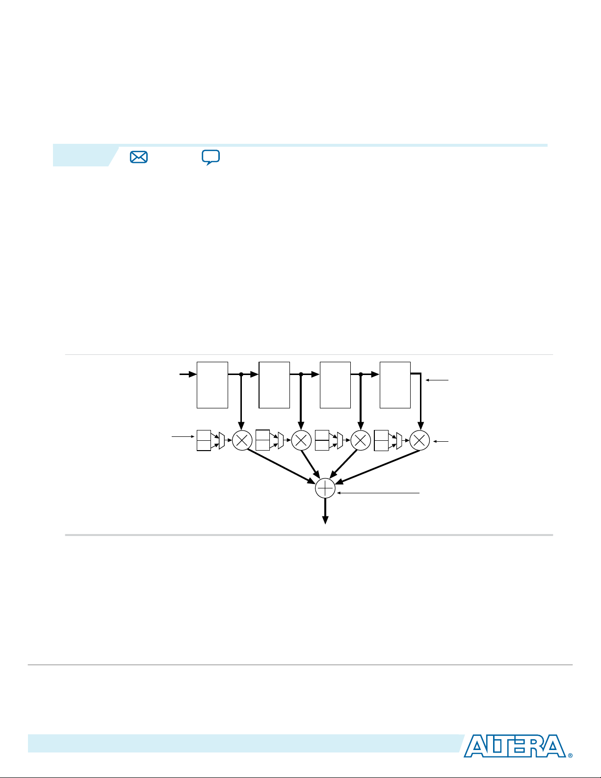
Figure 1-1: Basic FIR Filter with Weighted Tapped Delay Line
To design a filter, identify coefficients that match the frequency response you specify for the system. These
coefficients determine the response of the filter. You can change which signal frequencies pass through
the filter by changing the coefficient values in the parameter editor.
Altera DSP IP Core Features
©
2015 Altera Corporation. All rights reserved. ALTERA, ARRIA, CYCLONE, ENPIRION, MAX, MEGACORE, NIOS, QUARTUS and STRATIX words and logos are
trademarks of Altera Corporation and registered in the U.S. Patent and Trademark Office and in other countries. All other words and logos identified as
trademarks or service marks are the property of their respective holders as described at www.altera.com/common/legal.html. Altera warrants performance
of its semiconductor products to current specifications in accordance with Altera's standard warranty, but reserves the right to make changes to any
products and services at any time without notice. Altera assumes no responsibility or liability arising out of the application or use of any information,
product, or service described herein except as expressly agreed to in writing by Altera. Altera customers are advised to obtain the latest version of device
specifications before relying on any published information and before placing orders for products or services.
ISO
9001:2008
Registered
Page 5

1-2
FIR II IP Core Features
• Avalon® Streaming (Avalon-ST) interfaces
• DSP Builder ready
• Testbenches to verify the IP core
• IP functional simulation models for use in Altera-supported VHDL and Verilog HDL simulators
FIR II IP Core Features
• Exploiting maximal designs efficiency through hardware optimizations such as:
• Interpolation
• Decimation
• Symmetry
• Decimation half-band
• Time sharing
• Easy system integration using Avalon Streaming (Avalon-ST) interfaces.
• Memory and multiplier trade-offs to balance the implementation between logic elements (LEs) and
memory blocks (M512, M4K, M9K, M10K, M20K, or M144K).
• Support for run-time coefficient reloading capability and multiple coefficient banks.
• User-selectable output precision via truncation, saturation, and rounding.
UG-01072
2014.12.15
DSP IP Core Device Family Support
Altera offers the following device support levels for Altera IP cores:
• Preliminary support—Altera verifies the IP core with preliminary timing models for this device family.
The IP core meets all functional requirements, but might still be undergoing timing analysis for the
device family. You can use it in production designs with caution.
• Final support—Altera verifies the IP core with final timing models for this device family. The IP core
meets all functional and timing requirements for the device family. You can use it in production
designs.
Table 1-1: DSP IP Core Device Family Support
Device Family Support
Arria® II GX Final
Arria II GZ Final
Arria V Final
Arria 10 Final
Cyclone® IV Final
Cyclone V Final
MAX® 10 FPGA Final
Stratix® IV GT Final
Stratix IV GX/E Final
Altera Corporation
About the FIR II IP Core
Send Feedback
Page 6
UG-01072
2014.12.15
Device Family Support
Stratix V Final
Other device families No support
DSP IP Core Verification
Before releasing a version of an IP core, Altera runs comprehensive regression tests to verify its quality
and correctness. Altera generates custom variations of the IP core to exercise the various parameter
options and thoroughly simulates the resulting simulation models with the results verified against master
simulation models.
FIR II IP Core Release Information
Use the release information when licensing the IP core.
Table 1-2: Release Information
Item Description
DSP IP Core Verification
1-3
Version 14.1
Release Date December 2014
Ordering Code IP-FIRII
Product ID 00D8
Vendor ID 6AF7
Altera verifies that the current version of the Quartus II software compiles the previous version of each IP
core. Altera does not verify that the Quartus II software compiles IP core versions older than the previous
version. The Altera IP Release Notes lists any exceptions.
Related Information
• Altera IP Release Notes
• Errata for FIR II IP core in the Knowledge Base
FIR II IP Core Performance and Resource Utilization
Table 1-3: FIR II IP Core Performance—Arria V Devices
Typical expected performance using the Quartus II software with Arria V (5AGXFB3H4F40C4).
Parameters
ALM
Channel Wires Filter Type Coefficients M10K M20K Primary Secondary
DSP
Blocks
Memory Registers
f
MAX
(MHz)
8 2 Decimation — 1,607 24 0 — 1,232 64 30
About the FIR II IP Core
Send Feedback
8
Altera Corporation
Page 7

1-4
FIR II IP Core Performance and Resource Utilization
UG-01072
2014.12.15
Parameters
ALM
Channel Wires Filter Type Coefficients M10K M20K Primary Secondary
DSP
Blocks
Memory Registers
8 2 Decimation Write 2,120 24 0 — 1,298 141 30
8 2 Fractional
— 1,395 16 0 — 2,074 99 28
Rate
8 2 Fractional
Write 1,745 16 0 — 2,171 91 28
Rate
8 2 Fractional
— 1,493 16 0 — 2,167 117 28
Rate
8 2 Fractional
Write 1,852 16 0 — 2,287 116 27
Rate
8 2 Interpolation — 1,841 32 0 — 2,429 52 28
8 2 Interpolation Write 1,994 32 0 — 2,826 41 27
8 2 Interpolation Multiple
2,001 32 0 — 2,737 74 27
banks
f
MAX
(MHz)
8
1
2
0
0
2
8
9
8 2 Interpolation Multiple
banks;
2,700 32 0 — 2,972 130 28
2
Write
8 2 Single rate — 932 20 0 — 318 20 27
8
8 2 Single rate Write 1,057 20 0 — 713 3 27
9
8 1 Decimation — 329 3 1 — 321 33 30
1
8 1 Decimation Write 430 3 1 — 366 34 30
7
8 1 Decimation Multiple
banks
8 1 Decimation Multiple
banks;
395 3 3 — 483 44 31
0
510 3 3 — 472 40 29
1
Write
8 1 Fractional
Rate
8 1 Fractional
Rate
— 661 5 4 — 877 75 31
0
Write 788 5 4 — 936 98 30
9
Altera Corporation
About the FIR II IP Core
Send Feedback
Page 8

UG-01072
2014.12.15
FIR II IP Core Performance and Resource Utilization
1-5
Parameters
ALM
Channel Wires Filter Type Coefficients M10K M20K Primary Secondary
DSP
Blocks
Memory Registers
8 1 Interpolation — 381 5 0 — 442 32 27
8 1 Interpolation Write 514 5 0 — 540 27 27
8 1 Single Rate — 493 10 0 — 191 20 27
8 1 Single Rate Write 633 10 0 — 588 1 27
1 — Decimation — 220 3 0 — 158 27 31
1 super
— Decimation — 404 20 0 — 400 41 30
sample
1 super
— Decimation Write 505 20 0 — 785 35 30
sample
1 — Decimation Write 318 3 0 — 208 26 30
f
MAX
(MHz)
8
8
8
8
0
5
8
9
1 Half
Band
1 Half
Band
1 — Fractional
1 — Fractional
1 Half
Band
1 Half
Band
— Decimation — 234 3 0 — 192 34 30
8
— Decimation Write 320 3 0 — 232 27 30
9
— 297 3 0 — 504 57 31
Rate
0
Write 391 3 0 — 563 56 31
Rate
— Fractional
Rate
— Fractional
Rate
— 196 2 0 — 251 5 27
Write 266 2 0 — 301 15 28
0
7
0
1 — Interpolation — 266 5 0 — 290 30 27
8
1 super
sample
1 super
sample
— Interpolation — 717 32 0 — 903 45 30
8
— Interpolation Write 842 32 0 — 1,281 48 30
8
1 — Interpolation Write 405 5 0 — 380 15 27
About the FIR II IP Core
Send Feedback
8
Altera Corporation
Page 9
1-6
FIR II IP Core Performance and Resource Utilization
UG-01072
2014.12.15
Parameters
Channel Wires Filter Type Coefficients M10K M20K Primary Secondary
1 Half
— Interpolation — 254 3 0 — 293 8 31
ALM
DSP
Blocks
Memory Registers
Band
1 Half
— Interpolation Write 333 4 0 — 314 10 30
Band
1 — Single rate — 93 10 0 — 129 27 29
1 super
— Single rate — 262 20 0 — 307 41 30
sample
1 super
— Single rate Write 373 20 0 — 687 40 30
sample
1 — Single rate Write 228 10 0 — 519 16 30
1 Half
— Single rate — 189 5 0 — 254 63 30
Band
1 Half
— Single rate Write 272 5 0 — 496 29 31
Band
f
MAX
(MHz)
0
9
9
9
2
0
9
0
1 — Single rate Multiple
109 10 0 — 199 29 28
banks
1 — Single rate Multiple
395 10 0 — 361 19 28
banks;
Write
Table 1-4: FIR II IP Core Performance—Cyclone V Devices
Typical expected performance using the Quartus II software with Cyclone V (5CGXFC7D6F31C6) devices.
Parameters
ALM
Channel Wires Filter Type Coefficients M10K M20K Primary Secondary
DSP
Blocks
Memory Registers
8 2 Decimation — 1,607 24 0 — 1,231 46 27
8 2 Decimation Write 2,092 24 0 — 1,352 63 27
8 2 Fractional
— 1,852 16 0 — 3,551 309 25
Rate
8 2 Fractional
Write 2,203 16 0 — 3,675 269 25
Rate
3
2
f
MAX
(MHz)
3
3
4
5
8 2 Fractional
Altera Corporation
Rate
— 1,951 16 0 — 3,543 421 22
7
About the FIR II IP Core
Send Feedback
Page 10

UG-01072
2014.12.15
FIR II IP Core Performance and Resource Utilization
1-7
Parameters
Channel Wires Filter Type Coefficients M10K M20K Primary Secondary
8 2 Fractional
Write 2,301 16 0 — 3,601 476 25
ALM
DSP
Blocks
Memory Registers
Rate
8 2 Interpolation — 1,840 32 0 — 2,431 48 25
8 2 Interpolation Write 1,988 32 0 — 2,813 57 25
8 2 Interpolation Multiple
2,006 32 0 — 2,711 98 25
banks
8 2 Interpolation Multiple
2,704 32 0 — 2,990 100 25
banks;
Write
8 2 Single rate — 934 20 0 — 317 19 25
8 2 Single rate Write 1,053 20 0 — 704 12 25
8 1 Decimation — 474 3 1 — 541 50 27
f
MAX
(MHz)
0
5
2
3
0
2
1
5
8 1 Decimation Write 559 3 1 — 574 58 27
3
8 1 Decimation Multiple
banks
8 1 Decimation Multiple
banks;
544 3 3 — 691 83 27
5
636 3 3 — 677 82 27
5
Write
8 1 Fractional
Rate
8 1 Fractional
Rate
— 1,165 5 4 — 1,715 205 27
5
Write 1,287 5 4 — 1,770 198 27
5
8 1 Interpolation — 381 5 0 — 433 42 24
8
8 1 Interpolation Write 513 5 0 — 540 26 25
0
8 1 Single Rate — 493 10 0 — 191 18 24
9
8 1 Single Rate Write 624 10 0 — 563 26 25
1
About the FIR II IP Core
Send Feedback
Altera Corporation
Page 11

1-8
FIR II IP Core Performance and Resource Utilization
UG-01072
2014.12.15
Parameters
ALM
Channel Wires Filter Type Coefficients M10K M20K Primary Secondary
DSP
Blocks
Memory Registers
1 — Decimation — 219 3 0 — 159 23 28
1 super
— Decimation — 404 20 0 — 398 43 28
sample
1 super
— Decimation Write 503 20 0 — 774 46 25
sample
1 — Decimation Write 312 3 0 — 208 26 28
1 Half
— Decimation — 234 3 0 — 192 29 28
Band
1 Half
— Decimation Write 323 3 0 — 228 32 28
Band
1 — Fractional
— 422 3 0 — 723 94 31
Rate
1 — Fractional
Write 516 3 0 — 787 86 29
Rate
f
MAX
(MHz)
9
8
6
9
9
8
0
2
1 Half
Band
1 Half
Band
— Fractional
Rate
— Fractional
Rate
— 195 2 0 — 251 12 26
1
Write 267 2 0 — 299 15 25
2
1 — Interpolation — 262 5 0 — 296 25 25
2
1 super
sample
1 super
sample
— Interpolation — 708 32 0 — 914 34 27
2
— Interpolation Write 841 32 0 — 1,297 32 25
9
1 — Interpolation Write 400 5 0 — 382 12 25
8
1 Half
Band
1 Half
Band
— Interpolation — 288 3 0 — 456 13 29
0
— Interpolation Write 331 4 0 — 315 9 29
0
1 — Single rate — 87 10 0 — 142 14 25
3
1 super
sample
Altera Corporation
— Single rate — 258 20 0 — 315 33 26
0
About the FIR II IP Core
Send Feedback
Page 12
UG-01072
2014.12.15
FIR II IP Core Performance and Resource Utilization
1-9
Parameters
Channel Wires Filter Type Coefficients M10K M20K Primary Secondary
1 super
— Single rate Write 369 20 0 — 704 23 27
ALM
DSP
Blocks
Memory Registers
sample
1 — Single rate Write 227 10 0 — 535 0 25
1 Half
— Single rate — 187 5 0 — 273 44 28
Band
1 Half
— Single rate Write 274 5 0 — 506 19 27
Band
1 — Single rate Multiple
110 10 0 — 187 41 25
banks
1 — Single rate Multiple
375 10 0 — 349 32 25
banks;
Write
Table 1-5: FIR II IP Core Performance—Stratix V Devices
Typical expected performance using the Quartus II software with Stratix V (5SGSMD4H2F35C2) devices.
Parameters
ALM
Channel Wires Filter Type Coefficients M10K M20K Primary Secondary
DSP
Blocks
Memory Registers
f
MAX
(MHz)
4
1
8
5
5
5
f
MAX
(MHz)
8 2 Decimation — 1,609 24 — 0 1,231 60 45
0
8 2 Decimation Write 2,319 24 — 0 2,077 66 45
0
8 2 Fractional
Rate
8 2 Fractional
Rate
8 2 Fractional
Rate
8 2 Fractional
Rate
— 1,350 16 — 0 2,099 88 44
8
Write 1,771 16 — 0 2,291 78 45
0
— 1,457 16 — 0 2,213 88 44
4
Write 1,873 16 — 0 2,418 89 45
0
8 2 Interpolation — 1,777 32 — 0 2,303 15 44
4
8 2 Interpolation Write 2,081 32 — 0 3,009 26 45
0
8 2 Interpolation Multiple
banks
1,825 32 — 0 2,473 39 43
0
About the FIR II IP Core
Send Feedback
Altera Corporation
Page 13

1-10
FIR II IP Core Performance and Resource Utilization
UG-01072
2014.12.15
Parameters
Channel Wires Filter Type Coefficients M10K M20K Primary Secondary
8 2 Interpolation Multiple
ALM
2,652 32 — 0 2,842 236 42
DSP
Blocks
Memory Registers
banks;
Write
8 2 Single rate — 920 20 — 0 332 2 44
8 2 Single rate Write 1,359 20 — 0 1,323 1 45
8 1 Decimation — 340 3 — 0 324 25 45
8 1 Decimation Write 463 3 — 0 457 29 45
8 1 Decimation Multiple
466 3 — 0 569 42 45
banks
8 1 Decimation Multiple
577 3 — 0 567 41 45
banks;
Write
f
MAX
(MHz)
4
4
0
0
0
0
0
8 1 Fractional
Rate
8 1 Fractional
Rate
— 709 5 — 0 870 45 45
0
Write 852 5 — 0 991 65 45
0
8 1 Interpolation — 216 5 — 0 197 13 45
0
8 1 Interpolation Write 361 5 — 0 290 22 45
0
8 1 Single Rate — 483 10 — 0 212 4 44
7
8 1 Single Rate Write 783 10 — 0 894 4 45
0
1 — Decimation — 215 3 — 0 175 10 45
0
1 super
sample
1 super
sample
— Decimation — 547 20 — 0 1,167 88 45
0
— Decimation Write 989 20 — 0 2,214 105 45
0
1 — Decimation Write 331 3 — 0 310 7 45
Altera Corporation
0
About the FIR II IP Core
Send Feedback
Page 14

UG-01072
2014.12.15
FIR II IP Core Performance and Resource Utilization
1-11
Parameters
Channel Wires Filter Type Coefficients M10K M20K Primary Secondary
1 Half
— Decimation — 226 3 — 0 206 16 45
ALM
DSP
Blocks
Memory Registers
Band
1 Half
— Decimation Write 343 3 — 0 327 18 45
Band
1 — Fractional
— 252 3 — 0 318 21 44
Rate
1 — Fractional
Write 353 3 — 0 380 13 45
Rate
1 Half
Band
1 Half
Band
— Fractional
Rate
— Fractional
Rate
— 140 2 — 0 185 13 45
Write 214 2 — 0 235 21 45
1 — Interpolation — 168 5 — 0 127 19 45
1 super
— Interpolation — 573 32 — 0 1,084 51 44
sample
f
MAX
(MHz)
0
0
5
0
0
0
0
6
1 super
sample
— Interpolation Write 870 32 — 0 1,774 136 45
0
1 — Interpolation Write 313 5 — 0 196 5 45
0
1 Half
Band
1 Half
Band
— Interpolation — 253 3 — 0 292 9 45
0
— Interpolation Write 370 4 — 0 418 9 45
0
1 — Single rate — 226 10 — 0 706 31 44
7
1 _
ssample
1 _
ssample
— Single rate — 468 20 — 0 1,354 53 45
0
— Single rate Write 927 20 — 0 2,267 203 45
0
1 — Single rate Write 524 10 — 0 1,391 31 50
0
1 Half
Band
— Single rate — 195 5 — 0 270 50 45
0
1 Half
Band
About the FIR II IP Core
Send Feedback
— Single rate Write 351 5 — 0 645 28 45
0
Altera Corporation
Page 15

1-12
FIR II IP Core Performance and Resource Utilization
UG-01072
2014.12.15
Parameters
ALM
Channel Wires Filter Type Coefficients M10K M20K Primary Secondary
1 — Single rate Multiple
250 10 — 0 716 93 44
DSP
Blocks
Memory Registers
banks
1 — Single rate Multiple
671 10 — 0 1,228 50 45
banks;
Write
f
MAX
(MHz)
9
0
Altera Corporation
About the FIR II IP Core
Send Feedback
Page 16

2014.12.15
acds
quartus - Contains the Quartus II software
ip - Contains the Altera IP Library and third-party IP cores
altera - Contains the Altera IP Library source code
<IP core name> - Contains the IP core source files
www.altera.com
101 Innovation Drive, San Jose, CA 95134
FIR II IP Core Getting Started
2
UG-01072
Subscribe
Send Feedback
1.
Installing and Licensing IP Cores
The Altera IP Library provides many useful IP core functions for your production use without purchasing
an additional license. Some Altera MegaCore® IP functions require that you purchase a separate license
for production use. However, the OpenCore® feature allows evaluation of any Altera IP core in simulation
and compilation in the Quartus® II software. After you are satisfied with functionality and perfformance,
visit the Self Service Licensing Center to obtain a license number for any Altera product.
Figure 2-1: IP Core Installation Path
Note:
The default IP installation directory on Windows is <drive>:\altera\<version number>; on Linux it is
<home directory>/altera/ <version number>.
Related Information
• Altera Licensing Site
• Altera Software Installation and Licensing Manual
OpenCore Plus IP Evaluation
Altera's free OpenCore Plus feature allows you to evaluate licensed MegaCore IP cores in simulation and
hardware before purchase. You need only purchase a license for MegaCore IP cores if you decide to take
your design to production. OpenCore Plus supports the following evaluations:
©
2015 Altera Corporation. All rights reserved. ALTERA, ARRIA, CYCLONE, ENPIRION, MAX, MEGACORE, NIOS, QUARTUS and STRATIX words and logos are
trademarks of Altera Corporation and registered in the U.S. Patent and Trademark Office and in other countries. All other words and logos identified as
trademarks or service marks are the property of their respective holders as described at www.altera.com/common/legal.html. Altera warrants performance
of its semiconductor products to current specifications in accordance with Altera's standard warranty, but reserves the right to make changes to any
products and services at any time without notice. Altera assumes no responsibility or liability arising out of the application or use of any information,
product, or service described herein except as expressly agreed to in writing by Altera. Altera customers are advised to obtain the latest version of device
specifications before relying on any published information and before placing orders for products or services.
ISO
9001:2008
Registered
Page 17

2-2
FIR II IP Core OpenCore Plus Timeout Behavior
• Simulate the behavior of a licensed IP core in your system.
• Verify the functionality, size, and speed of the IP core quickly and easily.
• Generate time-limited device programming files for designs that include IP cores.
• Program a device with your IP core and verify your design in hardware.
OpenCore Plus evaluation supports the following two operation modes:
• Untethered—run the design containing the licensed IP for a limited time.
• Tethered—run the design containing the licensed IP for a longer time or indefinitely. This requires a
connection between your board and the host computer.
Note: All IP cores that use OpenCore Plus time out simultaneously when any IP core in the design times
out.
FIR II IP Core OpenCore Plus Timeout Behavior
All IP cores in a device time out simultaneously when the most restrictive evaluation time is reached. If
there is more than one IP core in a design, the time-out behavior of the other IP cores may mask the timeout behavior of a specific IP core .
All IP cores in a device time out simultaneously when the most restrictive evaluation time is reached. If
there is more than one IP core in a design, a specific IP core's time-out behavior may be masked by the
time-out behavior of the other IP cores. For IP cores, the untethered time-out is 1 hour; the tethered timeout value is indefinite. Your design stops working after the hardware evaluation time expires. The Quartus
II software uses OpenCore Plus Files (.ocp) in your project directory to identify your use of the OpenCore
Plus evaluation program. After you activate the feature, do not delete these files..
UG-01072
2014.12.15
When the evaluation time expires, the ast_source_data signal goes low.
Related Information
• AN 320: OpenCore Plus Evaluation of Megafunctions
IP Catalog and Parameter Editor
The Quartus II IP Catalog (Tools > IP Catalog) and parameter editor help you easily customize and
integrate IP cores into your project. You can use the IP Catalog and parameter editor to select, customize,
and generate files representing your custom IP variation.
Note:
The IP Catalog (Tools > IP Catalog) and parameter editor replace the MegaWizard™ Plug-In
Manager for IP selection and parameterization, beginning in Quartus II software version 14.0. Use
the IP Catalog and parameter editor to locate and paramaterize Altera IP cores.
The IP Catalog lists installed IP cores available for your design. Double-click any IP core to launch the
parameter editor and generate files representing your IP variation. The parameter editor prompts you to
specify an IP variation name, optional ports, and output file generation options. The parameter editor
generates a top-level Qsys system file (.qsys) or Quartus II IP file (.qip) representing the IP core in your
project. You can also parameterize an IP variation without an open project.
Altera Corporation
FIR II IP Core Getting Started
Send Feedback
Page 18
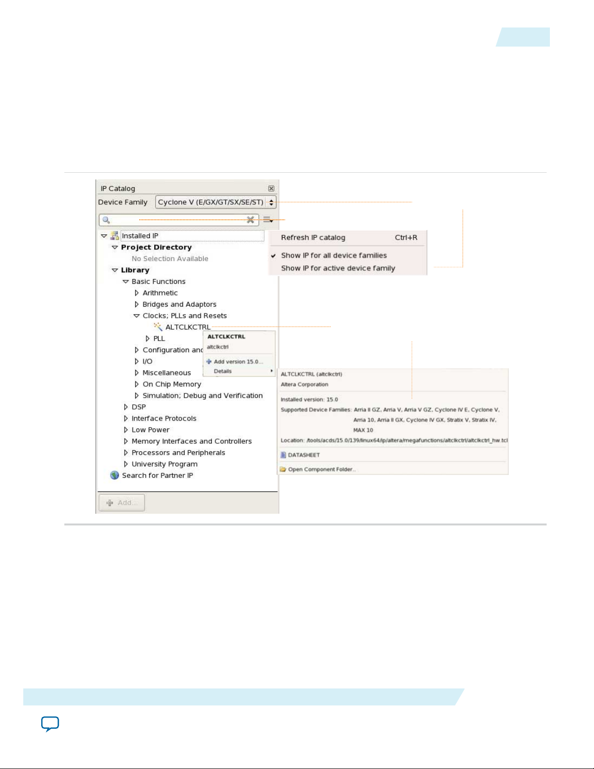
Search for installed IP cores
Double-click to customize, right-click for
detailed information
Show IP only for target device
UG-01072
2014.12.15
Specifying IP Core Parameters and Options
Use the following features to help you quickly locate and select an IP core:
• Filter IP Catalog to Show IP for active device family or Show IP for all device families. If you have no
project open, select the Device Family in IP Catalog.
• Type in the Search field to locate any full or partial IP core name in IP Catalog.
• Right-click an IP core name in IP Catalog to display details about supported devices, open the IP core's
installation folder, and view links to documentation.
• Click Search for Partner IP, to access partner IP information on the Altera website.
Figure 2-2: Quartus II IP Catalog
2-3
Note: The IP Catalog is also available in Qsys (View > IP Catalog). The Qsys IP Catalog includes
exclusive system interconnect, video and image processing, and other system-level IP that are not
available in the Quartus II IP Catalog. For more information about using the Qsys IP Catalog, refer
to Creating a System with Qsys in the Quartus II Handbook.
Specifying IP Core Parameters and Options
You can quickly configure a custom IP variation in the parameter editor. Use the following steps to
specify IP core options and parameters in the parameter editor. Refer to Specifying IP Core Parameters
and Options (Legacy Parameter Editors) for configuration of IP cores using the legacy parameter editor.
FIR II IP Core Getting Started
Send Feedback
Altera Corporation
Page 19

2-4
Specifying IP Core Parameters and Options
UG-01072
2014.12.15
1. In the IP Catalog (Tools > IP Catalog), locate and double-click the name of the IP core to customize.
The parameter editor appears.
2. Specify a top-level name for your custom IP variation. The parameter editor saves the IP variation
settings in a file named <your_ip>.qsys. Click OK.
3. Specify the parameters and options for your IP variation in the parameter editor, including one or
more of the following. Refer to your IP core user guide for information about specific IP core
parameters.
• Optionally select preset parameter values if provided for your IP core. Presets specify initial
parameter values for specific applications.
• Specify parameters defining the IP core functionality, port configurations, and device-specific
features.
• Specify options for processing the IP core files in other EDA tools.
4. Click Generate HDL, the Generation dialog box appears.
5. Specify output file generation options, and then click Generate. The IP variation files generate
according to your specifications.
6. To generate a simulation testbench, click Generate > Generate Testbench System.
7. To generate an HDL instantiation template that you can copy and paste into your text editor, click
Generate > HDL Example.
8. Click Finish. The parameter editor adds the top-level .qsys file to the current project automatically. If
you are prompted to manually add the .qsys file to the project, click Project > Add/Remove Files in
Project to add the file.
9. After generating and instantiating your IP variation, make appropriate pin assignments to connect
ports.
Altera Corporation
FIR II IP Core Getting Started
Send Feedback
Page 20

View IP port
and parameter
details
Apply preset parameters for
specific applications
Specify your IP variation name
and target device
UG-01072
2014.12.15
Figure 2-3: IP Parameter Editor
Files Generated for Altera IP Cores
2-5
Files Generated for Altera IP Cores
The Quartus II software generates the following IP core output file structure:
FIR II IP Core Getting Started
Send Feedback
Altera Corporation
Page 21

<your_testbench>_tb.csv
<your_testbench>_tb.spd
<your_ip>.cmp - VHDL component declaration file
<your_ip>.ppf - XML I/O pin information file
<your_ip>.qip - Lists IP synthesis files
<your_ip>.sip - Contains assingments for IP simulation files
<your_ip>.v or .vhd
Top-level IP synthesis file
<your_ip>.v or .vhd
Top-level simulation file
<simulator_setup_scripts>
<your_ip>.qsys - System or IP integration file
<your_ip>_bb.v - Verilog HDL black box EDA synthesis file
<your_ip>_inst.v or .vhd - Sample instantiation template
<your_ip>_generation.rpt - IP generation report
<your_ip>.debuginfo - Contains post-generation information
<your_ip>.html - Connection and memory map data
<your_ip>.bsf - Block symbol schematic
<your_ip>.spd - Combines simulation scripts for multiple cores
<your_ip>_tb.qsys
Testbench system file
<your_ip>.sopcinfo - Software tool-chain integration file
<project directory>
<EDA tool setup
scripts>
<your_ip>
IP variation files
<testbench>_tb
testbench system
sim
Simulation files
synth
IP synthesis files
sim
simulation files
<EDA tool name>
Simulator scripts
<testbench>_tb
<ip subcores> n
Subcore libraries
sim
Subcore
Simulation files
synth
Subcore
synthesis files
<HDL files>
<HDL files>
<your_ip> n
IP variation files
testbench files
2-6
Files Generated for Altera IP Cores
Figure 2-4: IP Core Generated Files
UG-01072
2014.12.15
Altera Corporation
Table 2-1: IP Core Generated Files
File Name Description
<my_ip>.qsys
<system>.sopcinfo Describes the connections and IP component parameterizations in
The Qsys system or top-level IP variation file. <my_ip> is the name
that you give your IP variation.
your Qsys system. You can parse its contents to get requirements
when you develop software drivers for IP components.
Downstream tools such as the Nios II tool chain use this file.
The .sopcinfo file and the system.h file generated for the Nios II tool
chain include address map information for each slave relative to each
master that accesses the slave. Different masters may have a different
address map to access a particular slave component.
FIR II IP Core Getting Started
Send Feedback
Page 22

UG-01072
2014.12.15
Files Generated for Altera IP Cores
File Name Description
<my_ip>.cmp The VHDL Component Declaration (.cmp) file is a text file that
contains local generic and port definitions that you can use in VHDL
design files.
2-7
<my_ip>.html
A report that contains connection information, a memory map
showing the address of each slave with respect to each master to
which it is connected, and parameter assignments.
<my_ip>_generation.rpt IP or Qsys generation log file. A summary of the messages during IP
generation.
<my_ip>.debuginfo Contains post-generation information. Used to pass System Console
and Bus Analyzer Toolkit information about the Qsys interconnect.
The Bus Analysis Toolkit uses this file to identify debug components
in the Qsys interconnect.
<my_ip>.qip
Contains all the required information about the IP component to
integrate and compile the IP component in the Quartus II software.
<my_ip>.csv Contains information about the upgrade status of the IP component.
<my_ip>.bsf A Block Symbol File (.bsf) representation of the IP variation for use
in Quartus II Block Diagram Files (.bdf).
<my_ip>.spd
Required input file for ip-make-simscript to generate simulation
scripts for supported simulators. The .spd file contains a list of files
generated for simulation, along with information about memories
that you can initialize.
<my_ip>.ppf The Pin Planner File (.ppf) stores the port and node assignments for
IP components created for use with the Pin Planner.
<my_ip>_bb.v You can use the Verilog black-box (_bb.v) file as an empty module
declaration for use as a black box.
<my_ip>.sip Contains information required for NativeLink simulation of IP
components. You must add the .sip file to your Quartus project.
<my_ip>_inst.v or _inst.vhd HDL example instantiation template. You can copy and paste the
contents of this file into your HDL file to instantiate the IP variation.
<my_ip>.regmap If the IP contains register information, the .regmap file generates.
The .regmap file describes the register map information of master
and slave interfaces. This file complements the .sopcinfo file by
providing more detailed register information about the system. This
enables register display views and user customizable statistics in
System Console.
FIR II IP Core Getting Started
Send Feedback
Altera Corporation
Page 23

2-8
Simulating Altera IP Cores in other EDA Tools
File Name Description
UG-01072
2014.12.15
<my_ip>.svd
<my_ip>.v
or
<my_ip>.vhd
mentor/
aldec/
/synopsys/vcs
/synopsys/vcsmx
Allows HPS System Debug tools to view the register maps of
peripherals connected to HPS within a Qsys system.
During synthesis, the .svd files for slave interfaces visible to System
Console masters are stored in the .sof file in the debug section.
System Console reads this section, which Qsys can query for register
map information. For system slaves, Qsys can access the registers by
name.
HDL files that instantiate each submodule or child IP core for
synthesis or simulation.
Contains a ModelSim® script msim_setup.tcl to set up and run a
simulation.
Contains a Riviera-PRO script rivierapro_setup.tcl to setup and run a
simulation.
Contains a shell script vcs_setup.sh to set up and run a VCS
®
simulation.
Contains a shell script vcsmx_setup.sh and synopsys_ sim.setup file to
set up and run a VCS MX® simulation.
/cadence
Contains a shell script ncsim_setup.sh and other setup files to set up
and run an NCSIM simulation.
/submodules Contains HDL files for the IP core submodule.
<child IP cores>/ For each generated child IP core directory, Qsys generates /synth and /
sim sub-directories.
Simulating Altera IP Cores in other EDA Tools
The Quartus II software supports RTL and gate-level design simulation of Altera IP cores in supported
EDA simulators. Simulation involves setting up your simulator working environment, compiling
simulation model libraries, and running your simulation.
You can use the functional simulation model and the testbench or example design generated with your IP
core for simulation. The functional simulation model and testbench files are generated in a project
subdirectory. This directory may also include scripts to compile and run the testbench. For a complete list
of models or libraries required to simulate your IP core, refer to the scripts generated with the testbench.
You can use the Quartus II NativeLink feature to automatically generate simulation files and scripts.
NativeLink launches your preferred simulator from within the Quartus II software.
Altera Corporation
FIR II IP Core Getting Started
Send Feedback
Page 24

Post-fit timing
simulation netlist
Post-fit timing
simulation (3)
Post-fit functional
simulation netlist
Post-fit functional
simulation
Analysis & Synthesis
Fitter
(place-and-route)
TimeQuest Timing Analyzer
Device Programmer
Quartus II
Design Flow
Gate-Level Simulation
Post-synthesis
functional
simulation
Post-synthesis functional
simulation netlist
(Optional) Post-fit
timing simulation
RTL Simulation
Design Entry
(HDL, Qsys, DSP Builder)
Altera Simulation
Models
EDA
Netlist
Writer
UG-01072
2014.12.15
Figure 2-5: Simulation in Quartus II Design Flow
DSP Builder Design Flow
2-9
Note: Post-fit timing simulation is supported only for Stratix IV and Cyclone IV devices in the current
version of the Quartus II software. Altera IP supports a variety of simulation models, including
simulation-specific IP functional simulation models and encrypted RTL models, and plain text
RTL models. These are all cycle-accurate models. The models support fast functional simulation of
your IP core instance using industry-standard VHDL or Verilog HDL simulators. For some cores,
only the plain text RTL model is generated, and you can simulate that model. Use the simulation
models only for simulation and not for synthesis or any other purposes. Using these models for
synthesis creates a nonfunctional design.
Related Information
Simulating Altera Designs
DSP Builder Design Flow
DSP Builder shortens digital signal processing (DSP) design cycles by helping you create the hardware
representation of a DSP design in an algorithm-friendly development environment.
This IP core supports DSP Builder. Use the DSP Builder flow if you want to create a DSP Builder model
that includes an IP core variation; use IP Catalog if you want to create an IP core variation that you can
instantiate manually in your design. For more information about the DSP Builder flow, refer to the
FIR II IP Core Getting Started
Send Feedback
Altera Corporation
Page 25

2-10
DSP Builder Design Flow
Related Information
Using MegaCore Functions chapter in the DSP Builder Handbook.
UG-01072
2014.12.15
Altera Corporation
FIR II IP Core Getting Started
Send Feedback
Page 26

2014.12.15
www.altera.com
101 Innovation Drive, San Jose, CA 95134
FIR II IP Core Parameters
3
UG-01072
Subscribe
Send Feedback
You define a FIR filter by its coefficients. You specify the filter settings and coefficient options in the
parameter editor.
The FIR II IP core provides a default 37-tap coefficient set regardless of the configurations from filter
settings. The scaled value and fixed point value are recalculated based on the coefficient bit width setting.
The higher the coefficient bit width, the closer the fixed frequency response is to the intended original
frequency response with the expense of higher resource usage.
You can load the coefficients from a file. For example, you can create the coefficients in another applica‐
tion such as MATLAB or a user-created program, save the coefficients to a file, and import them into the
FIR II IP core.
Related Information
Loading Coefficients from a File on page 3-3
Filter Specification Parameters
Table 3-1: Filter Specification Parameters
Parameter Value Description
Filter Settings
Filter Type Single Rate
Specifies the type of FIR filter.
Decimation
Interpolation
Fractional Rate
Interpolation Factor 1 to 128 Specifies the number of extra points to generate
between the original samples.
Decimation Factor 1 to 128 Specifies the number of data points to remove
between the original samples.
Number of Channels 1–128 Specifies the number of unique input channels to
process.
Frequency Specification
©
2015 Altera Corporation. All rights reserved. ALTERA, ARRIA, CYCLONE, ENPIRION, MAX, MEGACORE, NIOS, QUARTUS and STRATIX words and logos are
trademarks of Altera Corporation and registered in the U.S. Patent and Trademark Office and in other countries. All other words and logos identified as
trademarks or service marks are the property of their respective holders as described at www.altera.com/common/legal.html. Altera warrants performance
of its semiconductor products to current specifications in accordance with Altera's standard warranty, but reserves the right to make changes to any
products and services at any time without notice. Altera assumes no responsibility or liability arising out of the application or use of any information,
product, or service described herein except as expressly agreed to in writing by Altera. Altera customers are advised to obtain the latest version of device
specifications before relying on any published information and before placing orders for products or services.
ISO
9001:2008
Registered
Page 27

3-2
Filter Specification Parameters
Parameter Value Description
UG-01072
2014.12.15
Clock Frequency
1–500 Specifies the frequency of the input clock.
(MHz)
Clock Slack Integer Enables you to control the amount of pipelining
independently of the clock frequency and
therefore independently of the clock to sample
rate ratio.
Input Sample Rate
Integer Specifies the sample rate of the incoming data.
(MSPS)
Coefficient Options
Coefficient Scaling Auto
None
Specifies the coefficient scaling mode. Select Auto
to apply a scaling factor in which the maximum
coefficient value equals the maximum possible
value for a given number of bits. Select None to
read in pre-scaled integer values for the
coefficients and disable scaling.
Coefficient Data
Type
Signed Binary
Signed Fractional Binary
Specifies the coefficient input data type. Select
Signed Fractional Binary to monitor which bits
are preserved and which bits are removed during
the filtering process.
Coefficient Bit
Width
2–32 Specifies the width of the coefficients. The default
value is 8 bits.
Coefficient
Fractional Bit Width
0–32 Specifies the width of the coefficient data input
into the filter when you select Signed Fractional
Binary as your coefficient data type.
Coefficients Reload Options
Coefficients Reload — Turn on this option to allow coefficient reloading.
This option allows you to change coefficient
values during run time. When this option is
turned on, additional input ports are added to the
filter.
Base Address Integer Specifies the base address of the memory-mapped
coefficients.
Read/Write mode Read
Write
Specifies the read and write mode that determines
the type of address decode to build.
Read/Write
Flow Control
Altera Corporation
FIR II IP Core Parameters
Send Feedback
Page 28

UG-01072
2014.12.15
Coefficient Parameters
Parameter Value Description
3-3
Back Pressure
— Turn on this option to enable backpressure
Support
Coefficient Parameters
Table 3-2: Filter Specification Parameters
Parameter Value Description
Coefficient Options
L-th Band Filter All taps
Half band
3rd–5th
Coefficient Scaling Auto
None
support. When this option is turned on, the sink
signals the source to stop the flow of data when its
FIFO buffers are full or when there is congestion
on its output port.
Specifies the appropriate L-band Nyquist filters.
Every Lth coefficient of these filters is zero,
counting out from the center tap.
Specifies the coefficient scaling mode. Select Auto
to apply a scaling factor in which the maximum
coefficient value equals the maximum possible
value for a given number of bits. Select None to
read in pre-scaled integer values for the
coefficients and disable scaling.
Coefficient Data
Type
Signed Binary
Signed Fractional Binary
Specifies the coefficient input data type. Select
Signed Fractional Binary to monitor which bits
are preserved and which bits are removed during
the filtering process.
Coefficient Bit
Width
Coefficient
Fractional Bit Width
2–32 Specifies the width of the coefficients. The default
value is 8 bits.
0–32 Specifies the width of the coefficient data input
into the filter when you select Signed Fractional
Binary as your coefficient data type.
Frequency Response Display
Edit Current Bank 0–Number of coefficient bank-1Specifies the coefficient bank to display in the
coefficient table and frequency response graph.
Import from file URL Specifies the file from which to load coefficients. .
Loading Coefficients from a File
When you import a coefficient set, the wizard shows the frequency response of the floating-point
coefficients in blue and the frequency response of the fixed-point coefficients in red.
FIR II IP Core Parameters
Send Feedback
Altera Corporation
Page 29

3-4
Input and Output Options
The FIR II IP core supports scaling on the coefficient set.
1. Click Import coefficients, in the File name box, specify the name of the .txt file containing the
coefficient set.
• In the .txt file, separate the coefficients file by either white space or commas or both.
• Use new lines to separate banks.
• You may use blank lines as the FIR II IP core ignores them.
• You may use floating-point or fixed-point numbers, and scientific notation.
• Use a # character to add comments.
• Specify an array of coefficient sets to support multiple coefficient sets.
• Specify the number of rows to specify the number of banks.
• All coefficient sets must have the same symmetry type and number of taps. For example:
# bank 1 and 2 are symmetric
1, 2, 3, 2, 1
1 3 4 3 1
# bank 3 is anti-symmetric
1 2 0 -2 -1
# bank 4 is asymmetric
1,2,3,4,5
UG-01072
2014.12.15
Note:
The file must have a minimum of five non-zero coefficients.
2. Click Apply to import the coefficient set.
Input and Output Options
Table 3-3: Input and Output Options
Parameter Value Description
Input Options
Input Data Type Signed Binary
Signed Fractional
Binary
Input Bit Width 1–32 Specifies the width of the input data sent to the
Input Fractional Bit Width 0–32 Specifies the width of the data input into the filter
Specifies whether the input data is in a signed
binary or a signed fractional binary format. Select
Signed Fractional Binary to monitor which bits
the IP core preserves and which bits it removes
during the filtering process.
filter.
when you select Signed Fractional Binary as your
input data type.
Output Options
Altera Corporation
FIR II IP Core Parameters
Send Feedback
Page 30

UG-01072
2014.12.15
Signed Fractional Binary
Parameter Value Description
3-5
Output Data Type Signed Binary
Signed Fractional
Binary
Specifies whether the output data is in a signed
binary or a signed fractional binary format. Select
Signed Fractional Binary to monitor which bits
the IP core preserves and which bits it removes
during the filtering process.
Output Bit Width 0–32 Specifies the width of the output data (with limited
precision) from the filter.
Output Fractional Bit
Width
0–32 Specifies the width of the output data (with limited
precision) from the filter when you select Signed
Fractional Binary as your output data.
Output MSB rounding Truncation/
Saturating
Specifies whether to truncate or saturate the most
significant bit (MSB).
MSB Bits to Remove 0–32 Specifies the number of MSB bits to truncate or
saturate. The value must not be greater than its
corresponding integer bits or fractional bits.
Output LSB rounding Truncation/ Rounding Specifies whether to truncate or round the least
significant bit (LSB).
LSB Bits to Remove 0–32 Specifies the number of LSB bits to truncate or
round. The value must not be greater than its
corresponding integer bits or fractional bits.
Signed Fractional Binary
The FIR II IP core supports two’s complement, signed fractional binary notation, which allows you to
monitor which bits the IP core preserves and which bits it removes during filtering. A signed binary
fractional number has the format:
<sign> <integer bits>.<fractional bits>
A signed binary fractional number is interpreted as shown below:
<sign> <x1 integer bits>.<y1 fractional bits> Original input data
<sign> <x2 integer bits>.<y2 fractional bits> Original coefficient data
<sign> <i integer bits>.<y1 + y2 fractional bits> Full precision after FIR calculation
<sign> <x3 integer bits>.<y3 fractional bits> Output data after limiting precision
where i = ceil(log2(number of coefficients)) + x1 + x
For example, if the number has 3 fractional bits and 4 integer bits plus a sign bit, the entire 8-bit integer
number is divided by 8, which gives a number with a binary fractional component.
The total number of bits equals to the sign bits + integer bits + fractional bits. The sign + integer bits is
equal to Input Bit Width – Input Fractional Bit Width with a constraint that at least 1 bit must be
specified for the sign.
2
FIR II IP Core Parameters
Send Feedback
Altera Corporation
Page 31

D15
D14
D13
D12
D11
D10
D9
D8
.
.
D0
D9
D8
.
.
D0
Bits Removed from MSB
Full
Precision
Limited
Precision
D15
D14
.
.
.
.
D4
D3
D2
D1
D0
D11
D10
.
.
.
D1
D0
Bits Removed from LSB
Full
Precision
Limited
Precision
D15
D14
D13
D12
.
.
.
D3
D2
D1
D0
D10
D9
.
.
.
D1
D0
Bits Removed from both MSB & LSB
Full
Precision
Limited
Precision
3-6
MSB and LSB Truncation, Saturation, and Rounding
MSB and LSB Truncation, Saturation, and Rounding
The output options on the parameter editor allow you to truncate or saturate the MSB and to truncate or
round the LSB. Saturation, truncation, and rounding are non-linear operations.
Table 3-4: Options for Limiting Precision
UG-01072
2014.12.15
Bit
Option Result
Range
TruncateIn truncation, the filter disregards specified bits..
MSB
Saturate In saturation, if the filtered output is greater than the
maximum positive or negative value that can be
represented, the output is forced (or saturated) to the
maximum positive or negative value.
TruncateSame process as for MSB.
LSB
Round The output is rounded away from zero.
Figure 3-1: Removing Bits from the MSB and LSB
Memory and Multiplier Trade-Offs
Table 3-5: Implementation Options
Altera Corporation
Resource Optimization Settings
When the Quartus II software synthesizes your design to logic, it often creates delay blocks. The FIR II IP
core tries to balance the implementation between logic elements (LEs) and memory blocks (M512, M4K,
M9K, or M144K). The exact trade-off depends on the target FPGA family, but generally the trade-off
attempts to minimize the absolute silicon area used. For example, if a block of RAM occupies the silicon
area of two logic array blocks (LABs), a delay requiring more than 20 LEs (two LABs) is implemented as a
block of RAM. However, you want to influence this trade-off.
Parameter Value Description
FIR II IP Core Parameters
Send Feedback
Page 32

UG-01072
2014.12.15
Using CDelay RAM Block Threshold
Parameter Value Description
3-7
Device Family Menu of supported
Specifies the target device family.
devices
Speed grade Fast, medium, slow Specifies the speed grade of the target device to
balance the size of the hardware against the resources
required to meet the clock frequency.
CDelay RAM Block
Threshold
CDual Mem Dist
RAM Threshold
Integer Specifies the balance of resources between LEs/Small
RAM block threshold in bits.
Integer Specifies the balance of resources between small to
medium RAM block threshold in bits.
M-RAM Threshold Integer Specifies the balance of resources between medium to
large RAM block threshold in bits.
Hard Multiplier
Threshold
Integer Specifies the balance of resources between LEs/ DSP
block multiplier threshold in bits. The default value is
-1.
Symmetry Option
Symmetry Mode Non Symmetry
Symmetrical
Specifies whether your filter design uses nonsymmetric, symmetric, or anti-symmetric coefficients.
The default value is Non Symmetry.
Anti-Symmetrical
These topics describe the memory and multiplier threshold trade-offs, and provide some usage examples.
Using CDelay RAM Block Threshold
This threshold is the trade-off between simple delay LEs and small ROM blocks. If any delay’s size is such
that the number of LEs is greater than this parameter, the IP core implements delay as block RAM.
1. To make more delays using block RAM, enter a lower number, such as a value in the range of 20–30.
2. To use fewer block memories, enter a larger number, such as 100.
3. To never use block memory for simple delays, enter a very large number, such as 10000.
4. Implement delays of less than three cycles in LEs because of block RAM behavior.
Note:
This threshold only applies to implementing simple delays in memory blocks or logic elements.
You cannot push dual memories back into logic elements.
Using CDual Mem Dist RAM Threshold
This threshold is trade-off between small and medium RAM blocks. This threshold is similar to the Using
LEs / Small RAM Block Threshold except that it applies only to the dual-port memories.
The IP core implements any dual-port memory in a block memory rather than logic elements, but for
some device families different sizes of block memory may be available. The threshold value determines
which medium-size RAM memory blocks IP core implements instead of small-memory RAM blocks. For
FIR II IP Core Parameters
Send Feedback
Altera Corporation
Page 33

3-8
Using M-RAM Threshold
example, the threshold that determines whether to use M9K blocks rather than MLAB blocks on
Stratix IV devices.
1. Set the default threshold value, to implement dual memories greater than 1,280 bits as M9K blocks and
dual memories less than or equal to 1,280 bits as MLABs.
2. Change this threshold to a lower value such as 200, to implement dual memories greater than 200 bits
as M9K blocks and dual memories less than or equal to 200 bits as MLAB blocks.
Note: For device families with only one type of memory block, this threshold has no effect.
Using M-RAM Threshold
This threshold is the trade-off between medium and large RAM blocks. For larger delays, implement
memory in medium-block RAM (M4K, M9K) or use larger M-RAM blocks (M512K, M144K).
1. Set the number of bits in a memory or delay greater than this threshold, to use M-RAM.
2. Set a large value such as the default of 1,000,000 bits, to never uses M-RAM blocks.
Using Hard Multiplier Threshold
This threshold is the trade-off between hard and soft multipliers. For devices that support hard multipliers
or DSP blocks, use these resources instead of a soft multiplier made from LEs. For example, a 2-bit × 10bit multiplier consumes very few LEs. The hard multiplier threshold value corresponds to the number of
LEs that save a multiplier. If the hard multiplier threshold value is 100, you are allowing 100 LEs.
Therefore, an 18 × 18 multiplier (that requires approximately 182–350 LEs) is not transferred to LEs
because it requires more LEs than the threshold value. However, the IP core implements a 16 × 4
multiplier that requires approximately 64 LEs as a soft multiplier with this setting.
UG-01072
2014.12.15
1. Set the default to always use hard multipliers. With this value, IP core implements a 24 × 18 multiplier
as two 18 × 18 multipliers.
2. Set a value of approximately 300 to keep 18 × 18 multipliers hard, but transform smaller multipliers to
LEs. The IP core implements a 24 × 18 multiplier as a 6 × 18 multiplier and an 18 × 18 multiplier, so
this setting builds the hybrid multipliers that you require.
3. Set a value of approximately 1,000 to implement the multipliers entirely as LEs. Essentially you are
allowing a high number (1000) of LEs to save using an 18 × 18 multiplier.
4. Set a value of approximately 10 to implement a 24 × 16 multiplier as a 36 × 36 multiplier. With the
value, you are not even allowing the adder to combine two multipliers. Therefore, the system has to
burn a 36 × 36 multiplier in a single DSP block.
Altera Corporation
FIR II IP Core Parameters
Send Feedback
Page 34

2014.12.15
FIR
Filter
xln_v
bankln_0[]
xln_(n-1)[]
xOut_v
xOut_c
xOut_0[]
xOut_(m-1)[]
ast_sink_valid
ast_sink_data[]
ast_sink_sop
ast_sink_eop
ast_sink_error
ast_source_valid
ast_source_data[]
ast_source_sop
ast_source_eop
ast_source_error
ast_source_channel
Controller
ast_sink_ready
ast_source_ready
FIR Compiler II MegaCore Function
Sink
Source
control signals
control signals
control signals
xln_0[]
bankln_(n-1)[]
www.altera.com
101 Innovation Drive, San Jose, CA 95134
FIR II IP Core Functional Description
4
UG-01072
Subscribe
Send Feedback
The FIR II IP core generates the Avalon-ST register transfer level (RTL) wrapper.
Figure 4-1: High Level Block Diagram of FIR II IP core with Avalon-ST Interface
FIR II IP Core Interfaces and Signals
The IP core uses an interface controller for the Avalon-ST wrapper that handles the flow control
mechanism. The IP core communicates control signals between the sink interface, FIR filter, and source
interface via the controller. When designing a datapath that includes the FIR II IP core, you might not
need backpressure if you know the downstream components can always receive data. You might achieve a
©
2015 Altera Corporation. All rights reserved. ALTERA, ARRIA, CYCLONE, ENPIRION, MAX, MEGACORE, NIOS, QUARTUS and STRATIX words and logos are
trademarks of Altera Corporation and registered in the U.S. Patent and Trademark Office and in other countries. All other words and logos identified as
trademarks or service marks are the property of their respective holders as described at www.altera.com/common/legal.html. Altera warrants performance
of its semiconductor products to current specifications in accordance with Altera's standard warranty, but reserves the right to make changes to any
products and services at any time without notice. Altera assumes no responsibility or liability arising out of the application or use of any information,
product, or service described herein except as expressly agreed to in writing by Altera. Altera customers are advised to obtain the latest version of device
specifications before relying on any published information and before placing orders for products or services.
ISO
9001:2008
Registered
Page 35

4-2
Avalon-ST Interfaces in DSP IP Cores
higher clock rate by driving the ast_source_ready signal of the FIR II IP core high, and not connecting
the ast_sink_ready signal.
The sink and source interfaces implement the Avalon-ST protocol, which is a unidirectional flow of data.
The number of bits per symbol represents the data width and the number of symbols per beat is the
number of channel wires. The IP core symbol type supports signed and unsigned binary format. The
ready latency on the FIR II IP core is 0.
The clock and reset interfaces drive or receive the clock and reset signals to synchronize the Avalon-ST
interfaces and provide reset connectivity.
Related Information
Avalon Interface Specifications
For more information about the Avalon-ST interface properties, protocol and the data transfer timing
Avalon-ST Interfaces in DSP IP Cores
Avalon-ST interfaces define a standard, flexible, and modular protocol for data transfers from a source
interface to a sink interface.
The input interface is an Avalon-ST sink and the output interface is an Avalon-ST source. The Avalon-ST
interface supports packet transfers with packets interleaved across multiple channels.
Avalon-ST interface signals can describe traditional streaming interfaces supporting a single stream of
data without knowledge of channels or packet boundaries. Such interfaces typically contain data, ready,
and valid signals. Avalon-ST interfaces can also support more complex protocols for burst and packet
transfers with packets interleaved across multiple channels. The Avalon-ST interface inherently synchro‐
nizes multichannel designs, which allows you to achieve efficient, time-multiplexed implementations
without having to implement complex control logic.
UG-01072
2014.12.15
Avalon-ST interfaces support backpressure, which is a flow control mechanism where a sink can signal to
a source to stop sending data. The sink typically uses backpressure to stop the flow of data when its FIFO
buffers are full or when it has congestion on its output.
Related Information
• Avalon Interface Specifications
FIR II IP Core Avalon-ST Interfaces
Avalon-ST Sink Interface
The sink interface can handle single or multiple channels on a single wire and multiple channels on
multiple wires.
Altera Corporation
FIR II IP Core Functional Description
Send Feedback
Page 36

FIR Filter
xln_v
xln_0[7:0]
ast_sink_valid
ast_sink_data[7:0]
Controller
ast_sink_ready
FIR Compiler II MegaCore Function
Sink
sink_ready
control signals
UG-01072
2014.12.15
Single Channel on Single Wire
Figure 4-2: Single Channel on Single Wire Sink to FIR II IP Core
When transferring a single channel of 8bit data
Single Channel on Single Wire
4-3
FIR II IP Core Functional Description
Altera Corporation
Send Feedback
Page 37

FIR Filter
xln_v
xln_0[7:0]
ast_sink_valid
ast_sink_data[7:0]
Controller
ast_sink_ready
FIR Compiler II MegaCore Function
Sink
sink_ready
control signals
ast_sink_eop
ast_sink_sop
ast_sink_error
packet error
Avalon
Streaming
Interface
Signals Check
4-4
Multiple Channels on Single Wire
Multiple Channels on Single Wire
Figure 4-3: Multiple Channels on Single Wire Sink to FIR II IP core
When transferring a packet of data over multiple channels on a single wire. The data width of each
channel is 8 bits
UG-01072
2014.12.15
Altera Corporation
Multiple Channels on Multiple Wires
In this example, hardware optimization produces a TDM factor of 2, number of channel wires = 3, and
channels per wire = 2.
FIR II IP Core Functional Description
Send Feedback
Page 38

FIR Filter
xln_v
xln_0[7:0]
ast_sink_valid
ast_sink_data[23:0]
Controller
ast_sink_ready
FIR Compiler II MegaCore Function
Sink
xln_1[7:0]
xln_2[7:0]
control signals
ast_sink_eop
ast_sink_sop
ast_sink_error
sink_ready
packet error
Avalon
Streaming
Interface
Signals Check
UG-01072
2014.12.15
Multiple Channels on Multiple Wires
Figure 4-4: Multiple Channels on Multiple Wires
The sink interface to the FIR II IP core when transferring a packet of data over multiple channels on
multiple wires. The data width of each channel is 8 bits. Number of channels = 6, clock rate = 200 MHz,
and sample rate = 100 MHz
4-5
FIR II IP Core Functional Description
Altera Corporation
Send Feedback
Page 39

clk
ast_sink_valid
ast_sink_data[7:0]
ast_sink_data[15:8]
ast_sink_data[23:16]
ast_sink_sop
ast_sink_eop
xln_v[7:0]
xln_0[7:0]
xln_1[7:0]
xln_2[7:0]
A0
B0 A1 B1 A2 B2
C0
D0 C1 D1 C2 D2
E0
F0 E1 F1 E2 F2
A0
B0 A1
B1 A2
B2
C0
D0 C1
D1 C2
D2
E0
F0 E1
F1 E2
F2
X
X
X
4-6
Avalon-ST Source Interface
Figure 4-5: Timing Diagram of Multiple Channels on Multiple Wires
The sink interface to the FIR II IP core when transferring a packet of data over multiple channels on
multiple wires. The data width of each channel is 8 bits. Number of channels = 6, clock rate = 200 MHz,
and sample rate = 100 MHz
Avalon-ST Source Interface
The source interface can handle single or multiple channels on a single wire and multiple channels on
multiple wires. The IP core includes an Avalon-ST FIFO in the source wrapper when the backpressure
support is turned on. The Avalon-ST FIFO controls the backpressure mechanism and catches the extra
cycles of data from the FIR II IP core after backpressure. On the input side of the FIR II IP core, driving
the enable_i signal low, causes the FIR II IP core to stop. From the output side, backpressure drives the
enable_i signal of the FIR II IP core. If the downstream module can accept data again, the FIR II IP core
is instantly re-enabled.
UG-01072
2014.12.15
Altera Corporation
When the packet size is greater than one (multichannel), the source interface expects your application to
supply the count of data starting from 1 to the packet size. When the source interface receives the valid
flag together with the data_count = 1, it starts sending out data by driving both the ast_source_sop and
ast_source_valid signals high. When data_count equals the packet size, the ast_source_eop signal is
driven high together with the ast_source_valid signal.
If the downstream components are not ready to accept any data, the source interface drives the
source_stall signal high to tell the design to stall.
FIR II IP Core Functional Description
Send Feedback
Page 40

FIR Filter
xOut_v
xOut_c
xOut_0[7:0]
ast_source_valid
ast_source_data
ast_source_sop
ast_source_eop
ast_source_error
ast_source_channel
Controller
ast_source_ready
FIR Compiler II MegaCore Function
Source
enable_i
xOut_1[7:0]
xOut_2[7:0]
source_stall
source_valid
Avalon
Streaming
SCFIFO
(Only available
when
backpressure
is turned on)
UG-01072
2014.12.15
Avalon-ST Source Interface
Figure 4-6: Multiple Channels on Multiple Wires
The FIR II IP core to the source interface when transferring a packet of data over multiple channels on
multiple wires.
4-7
FIR II IP Core Functional Description
Send Feedback
Altera Corporation
Page 41

clk
xOut_v
xOut_c[7:0]
xOut_0[7:0]
xOut_1[7:0]
xOut_2[7:0]
ast_source_valid
ast_source_data[7:0]
ast_source_data[15:8]
ast_source_data[23:16]
ast_source_sop
ast_source_eop
ast_source_channel
ast_source_error
A0
B0 A1 B1 A2 B2
C0
D0 C1
D1 C2
D2
E0
F0 E1
F1 E2
F2
0
1 0 1 0 1
A0
B0 A1
B1 A2
B2
C0
D0 C1 D1 C2 D2
E0
F0 E1 F1 E2 F2
0
1 0
1 0
1
X
X
X
X
00
4-8
FIR II IP Core Signals
Figure 4-7: Timing Diagram of Multiple Channels on Multiple Wires
The FIR II IP core to the source interface when transferring a packet of data over multiple channels on
multiple wires.
UG-01072
2014.12.15
FIR II IP Core Signals
Table 4-1: FIR II IP Core Signals with Avalon-ST Interface
clk Input 1 Clock signal for all internal FIR II IP core filter
reset_n Input 1 Asynchronous active low reset signal. Resets the FIR
coeff_in_clk Input 1 Clock signal for the coefficient reloading mechanism.
coeff_in_areset Input 1 Asynchronous active high reset signal for the
ast_sink_ready Output 1 FIR filter asserts this signal when can accept data in
Altera Corporation
ast_sink_valid Input 1 Assert this signal when the input data is valid. When
Signal Direction Width Description
registers.
II IP core filter control circuit on the rising edge of
clk.
This clock can have a lower rate than the system
clock.
coefficient reloading mechanism.
the current clock cycle. This signal is not available
when backpressure is turned off.
ast_sink_valid is not asserted, the FIR processing
stops until you re-assert the ast_sink_valid signal.
FIR II IP Core Functional Description
Send Feedback
Page 42

UG-01072
2014.12.15
FIR II IP Core Signals
Signal Direction Width Description
4-9
ast_sink_data Input (Data width +
Bank width) ×
the number of
channel input
wires
(PhysChanIn)
where,
Bank width=
Log2(Number
of coefficient
sets)
Sample input data. For a multichannel operation
(number of channel input wires > 1), the least signifi‐
cant bits of ast_sink_data are mapped to xln_0 of
the FIR II IP core filter.
For example:
ast_sink_data[7:0] --> xln_0[7:0]
ast_sink_data[15:8] --> xln_1[7:0]
ast_sink_data[23:16] --> xln_2[7:0]
For multiple coefficient banks, the most significant
bits of the channel data are mapped to the bank
input signal and the LSBs of the channel data are
mapped to the data input signal.
For example,
Single channel with 4 coefficient banks:
ast_sink_data[9:8] --> BankIn_0
ast_sink_data[7:0] --> xln_0
Multi-channel (4 channels) with 4 coefficient banks:
ast_sink_data[9:8] --> BankIn_0
ast_sink_data[7:0] --> xln_0
ast_sink_data[19:18] --> BankIn_1
ast_sink_data[17:10] --> xln_1
ast_sink_data[29:28] --> BankIn_2
ast_sink_data[27:20] --> xln_2
ast_sink_data[39:38] --> BankIn_3
ast_sink_data[37:30] --> xln_3
ast_sink_sop
Input 1 Marks the start of the incoming sample group. The
start of packet (SOP) is interpreted as a sample from
channel 0.
ast_sink_eop Input 1 Marks the end of the incoming sample group. If data
is associated with N channels, the end of packet
(EOP) must be driven high when the sample
belonging to the last channel (that is, channel N-1),
is presented at the data input.
FIR II IP Core Functional Description
Send Feedback
Altera Corporation
Page 43

4-10
FIR II IP Core Signals
Signal Direction Width Description
ast_sink_error Input 2 Error signal indicating Avalon-ST protocol
violations on the sink side:
• 00: No error
• 01: Missing SOP
• 10: Missing EOP
• 11: Unexpected EOP
Other types of errors are also marked as 11.
ast_source_ready Input 1 The downstream module asserts this signal if it is
able to accept data. This signal is not available when
backpressure is turned off.
ast_source_valid Output 1 The IP core asserts this signal when there is valid
data to output.
UG-01072
2014.12.15
ast_source_channel Output Log
(number of
2
channels per
Indicates the index of the channel whose result is
presented at the data output.
wire)
ast_source_data Output Data width ×
number of
channel output
wires
(PhysChanOut)
ast_source_sop Output 1 Marks the start of the outgoing FIR II IP core filter
FIR II IP core filter output. For a multichannel
operation (number of channel output wires > 1), the
least significant bits of ast_source_data are
mapped to xOut_0 of the FIR II IP core filter.
For example:
xOut_0[7:0] --> ast_source_data[7:0]
xOut_1[7:0] --> ast_source_data[15:8]
xOut_2[7:0]--> ast_source_data[23:16]
result group. If '1', a result corresponding to channel
0 is output.
ast_source_eop Output 1 Marks the end of the outgoing FIR II IP core filter
result group. If '1', a result corresponding to channels
per wire N-1 is output, where N is the number of
channels per wire.
ast_source_error Output 2 Error signal indicating Avalon-ST protocol
Altera Corporation
violations on the source side:
• 00: No error
• 01: Missing SOP
• 10: Missing EOP
• 11: Unexpected EOP
Other types of errors are also marked as 11.
FIR II IP Core Functional Description
Send Feedback
Page 44
Clock Rate = Sample Rate
Clock Rate = 2 x Sample Rate
Read
Read
Write
WriteSerialize
Deserialize
UG-01072
2014.12.15
FIR II IP Core Time-Division Multiplexing
Signal Direction Width Description
4-11
coeff_in_address Input Number of
Address input to write new coefficient data.
coefficients
coeff_in_we Input 1 Write enable for memory-mapped coefficients.
coeff_in_data Input Coefficient
Data coefficient input.
width
coeff_out_valid Output 1 Coefficient read valid signal.
coeff_out_data Output Coefficient
width
Data coefficient output. The coefficient in memory at
the address specified by coeff_in_address.
FIR II IP Core Time-Division Multiplexing
The FIR II IP core optimizes hardware utilization by using time-division multiplexing (TDM). The TDM
factor (or folding factor) is the ratio of the clock rate to the sample rate.
By clocking a FIR II IP core faster than the sample rate, you can reuse the same hardware. For example, by
implementing a filter with a TDM factor of 2 and an internal clock multiplied by 2, you can halve the
required hardware.
Figure 4-8: Time-Division Multiplexing to Save Hardware Resources
FIR II IP Core Functional Description
Send Feedback
Altera Corporation
Page 45

4-12
FIR II IP Core Multichannel Operation
To achieve TDM, the IP core requires a serializer and deserializer before and after the reused hardware
block to control the timing. The ratio of system clock frequency to sample rate determines the amount of
resource saving except for a small amount of additional logic for the serializer and deserializer.
Table 4-2: Estimated Resources Required for a 49-Tap Single Rate Symmetric FIR II IP core Filter
UG-01072
2014.12.15
Clock Rate
(MHz)
Sample Rate
(MSPS)
Logic Multipliers Memory Bits TDM Factor
72 72 2230 25 0 1
144 72 1701 13 468 2
288 72 1145 7 504 4
72 36 1701 13 468 2
When the sample rate equals the clock rate, the filter is symmetric and you only need 25 multipliers.
When you increase the clock rate to twice the sample rate, the number of multipliers drops to 13. When
the clock rate is set to 4 times the sample rate, the number of multipliers drops to 7. If the clock rate stays
the same while the new data sample rate is only 36 MSPS (million samples per second), the resource
consumption is the same as twice the sample rate case.
FIR II IP Core Multichannel Operation
You can build multichannel systems directly using the required channel count, rather than creating a
single channel system and scaling it up. The IP core uses vectors of wires to scale without having to cut
and paste multiple blocks.
You can vectorize the FIR II IP core. If data going into the block is a vector requiring multiple instances of
a FIR filter, teh IP core creates multiple FIR blocks in parallel behind a single FIR II IP core block. If a
decimating filter requires a smaller vector on the output, the data from individual filters is automatically
time-division multiplexed onto the output vector. This feature relieves the necessity of gluing filters
together with custom logic.
Vectorized Inputs
The data inputs and outputs for the FIR II IP core blocks can be vectors. Use this capability when the
clock rate is insufficiently high to carry the total aggregate data. For example, 10 channels at 20 MSPS
require 10 × 20 = 200 MSPS aggregate data rate. If you set the system clock rate to 100 MHz, two wires are
required to carry this data, and so the FIR II IP core uses a vector of width 2.
This approach is unlike traditional methods because you do not need to manually instantiate two FIR
filters and pass a single wire to each in parallel. Each FIR II IP core block internally vectorizes itself. For
example, a FIR II IP core block can build two FIR filters in parallel and wire one element of the vector up
to each FIR. The same paradigm is used on outputs, where high data rates on multiple wires are
represented as vectors.
The input and output wire counts are determined by each FIR II IP core based on the clock rate, sample
rate, and number of channels.
The output wire count is also affected by any rate changes in the FIR II IP core. If there is a rate change,
such interpolating by two, the output aggregate sample rate doubles. The output channels are then packed
Altera Corporation
FIR II IP Core Functional Description
Send Feedback
Page 46

clock
input_valid
input_data_channel_0
input_data_channel_1
input_channel
output_valid
TDM_output_data
output_channel
c0(0) c0(1) c0(2)
c1(0) c1(1) c1(2)
c0(0) c1(0) don’t care c0(1) c1(1) don’t care c0(2) c1(2)
UG-01072
2014.12.15
Channelization
Channelization
4-13
into the fewest number of wires (vector width) that will support that rate. For example, an interpolate by
two FIR II IP core filters might have two wires at the input, but three wires at the output.
Any necessary multiplexing and packing is performed by the FIR II IP core. The blocks connected to the
inputs and outputs must have the same vector widths. Vector width errors can usually be resolved by
carefully changing the sample rates.
The number of wires and the number of channels carried on each wire are determined by
parameterization, which you can specify using the following variables:
• clockRate is the system clock frequency (MHz).
• inputRate is the data sample rate per channel (MSPS).
• inputChannelNum is the number of channels. Channels are enumerated from 0 to inputChan‐
nelNum–1.
• The period (or TDM factor) is the ratio of the clock rate to the sample rate and determines the number
of available time slots.
• ChanWireCount is the number of channel wires required to carry all the channels. It can be calculated
by dividing the number of channels by the TDM factor. More specifically:
• PhysChanIn = Number of channel input wires
• PhysChanOut = Number of channel output wires
• ChanCycleCount is the number of channels carried per wire. It is calculated by dividing the number of
channels by the number of channels per wire. The channel signal counts from 0 to ChanCycleCount–
1. More specifically:
• ChansPerPhyIn = Number of channels per input wire
• ChansPerPhyOut = Number of channels per output wire
If the number of channels is greater than the clock period, multiple wires are required. Each FIR II IP core
in your design is internally vectorized to build multiple FIR filters in parallel.
Figure 4-9: Channelization of Two Channels with a TDM Factor of 3
A TDM factor of 3 combines two input channels into a single output wire. (inputChannelNum = 2,
ChanWireCount = 1, ChanCycleCount = 2). This example has three available time slots in the output
channel and every third time slot has a ‘don't care’ value when the valid signal is low. The value of the
channel signal while the valid signal is low does not matter.
FIR II IP Core Functional Description
Send Feedback
Altera Corporation
Page 47

clock
input_valid
input_data_channel_0
input_data_channel_1
input_data_channel_2
input_data_channel_3
input_channel
output_valid
output_data_wire_1
output_data_wire_2
output_channel
c0(0)
c0(1) c0(2)
c1(0) c1(1) c1(2)
c2(0) c2(1) c2(2)
c3(0) c3(1) c3(2)
c0(0) c0(1)
c0(2)
c1(0) c1(1) c1(2)
c2(0) c2(1)
c2(2)
c3(0) c3(1) c3(2)
don’t care
don’t care
don’t care
don’t care
valid
channel
data0
0
1
2
3
0
1
2
3
c0(0) c1(0) c2(0) c3(0) c0(1)
c1(1)
c2(1) c3(1)
valid
channel
data0
data1
0
1
0
1
0
1
0
1
c0(0) c1(0) c0(1) c1(1) c0(2)
c1(2)
c0(3) c1(3)
c2(0) c3(0) c2(1) c3(1) c2(2)
c3(2)
c2(3) c2(3)
4-14
Channelization
Figure 4-10: Channelization for Four Channels with a TDM Factor of 3
A TDM factor of 3 combines four input channels into two wires (inputChannelNum = 4,
ChanWireCount = 2, ChanCycleCount = 2). This example shows two wires to carry the four channels and
the cycle count is two on each wire. The channels are evenly distributed on each wire leaving the third
time slot as don't care on each wire.
UG-01072
2014.12.15
The channel signal is used for synchronization and scheduling of data. It specifies the channel data
separation per wire. Note that the channel signal counts from 0 to ChanCycleCount–1 in synchronization
with the data. Thus, for ChanCycleCount = 1, the channel signal is the same as the channel count,
enumerated from 0 to inputChannelNum–1.
For a case with single wire, the channel signal is the same as a channel count.
Figure 4-11: Four Channels on One Wire with No Invalid Cycles
For ChanWireCount > 1, the channel signal specifies the channel data separation per wire, rather than the
actual channel number. The channel signal counts from 0 to ChanCycleCount–1 rather than 0 to
inputChannelNum–1.
Figure 4-12: Four Channels on Two Wires with No Invalid Cycles
Altera Corporation
Notice that the channel signal remains a single wire, not a wire for each data wire. It counts from 0 to
ChanCycleCount–1.
FIR II IP Core Functional Description
Send Feedback
Page 48

valid
channel
data0
data0
data1
data1
c0(0) c0(1) c0(2) c0(3) c0(4)
c0(5)
c0(6) c0(7)
0
c1(0) c1(1) c1(2) c1(3) c1(4)
c1(5)
c1(6) c1(7)
c2(0) c2(1) c2(2) c2(3) c2(4)
c2(5)
c2(6) c2(7)
c3(0) c3(1) c3(2) c3(3) c3(4)
c3(5)
c3(6) c3(7)
clk
xln_v
xln_0
xln_1
xln_2
C0
C1 C2
C3 C4 C5
C6
C7 --
clk
xOut_v
xOut_1
xOut_2
xOut_0
C0 C1 C2
C3
C4 C5
C6 C7 --
clk
xln_v
xln_0
xln_1
xln_2
C0
C1
C2
xln_3
C3
UG-01072
2014.12.15
Figure 4-13: Four Channels on Four Wires
Channel Input and Output Format
The FIR II IP core requires the inputs and the outputs to be in the same format when the number of input
channel is more than one. The input data to the MegaCore must be arranged horizontally according to the
channels and vertically according to the wires. The outputs should then come out in the same order,
counting along horizontal row first, vertical column second.
Eight Channels on Three Wires
Figure 4-14: Eight Channels on Three Wires (Input)
Channel Input and Output Format
4-15
Figure 4-15: Eight Channels on Three Wires (Output)
Four Channels on Four Wires
Figure 4-16: Four Channels on Four Wires (Input)
FIR II IP Core Functional Description
Send Feedback
Altera Corporation
Page 49

clk
xOut_v
xOut_0
xOut_1
xOut_2
C0
C1
C2
xOut_3
C3
clk
xln_v
xln_0
xln_1
C0
C1
C2 C3
clk
xOut_v
xOut_0
xOut_1
C0
C1
C2 C3
4-16
15 Channels with 15 Valid Cycles and 17 Invalid Cycles
Figure 4-17: Four Channels on Four Wires (Output)
This result appears to be vertical, but that is because the number of cycles is 1, so on each wire there is
only space for one piece of data.
Figure 4-18: Four Channels on Four Wires with Double Clock Rate (Input)
UG-01072
2014.12.15
Figure 4-19: Four Channels on Four Wires with Double Clock Rate (Output)
15 Channels with 15 Valid Cycles and 17 Invalid Cycles
Sometimes invalid cycles are inserted between the input data. An example where the clock rate = 320,
sample rate = 10, yields a TDM factor of 32, inputChannelNum = 15, and interpolation factor is 10. In this
case, the TDM factor is greater than inputChannelNum. The optimization produces a filter with
PhysChanIn = 1, ChansPerPhyIn = 15, PhysChanOut = 5, and ChansPerPhyOut = 3.
The input data format in this case is 32 cycles long, which comes from the TDM factor. The number of
channels is 15, so the filter expects 15 valid cycles together in a block, followed by 17 invalid cycles. You
can insert extra invalid cycles at the end, but they must not interrupt the packets of data after the process
has started. If the input sample rate is less than the clock rate, the pattern is always the same: a repeating
cycle, as long as the TDM factor, with the number of channels as the number of valid cycles required, and
the remainder as invalid cycles.
Altera Corporation
FIR II IP Core Functional Description
Send Feedback
Page 50

areset
clk
xin_v[0]
xin_c[7:0]
xin_0[7:0]
xout_v[0]
xout_c[7:0]
xout_0[17:0]
xout_1[17:0]
xout_2[17:0]
xout_3[17:0]
xout_4[17:0]
1 0
1 2 3 4 5 6 7 8 9 10 11 12 13 14 15 8 1 2 3 4 5
1
0
1 2 0 1 2 0 1 2 0 1 2 0 1 2 0 1 2 0 1 2 0 1 2 0 1 2 0 1 2 0 1 2 0 1 2
8 16 24 6 12 18 0 3FFF93FFF2
3FFEB
32 40 48 24 30 36 0 3FFE4
3FFDD
3FFD6
56 64 72 42 48 54 0
3FFCF
3FFC83FFC1
80 88 96 60 66 72 0
3FFBA
3FFB3
3FFAC
104 112 120 78 84 90 0 3FFA53FF9E3FF97
areset
clk
xin_v[0]
xin_c[7:0]
xin_0[7:0]
xout_v[0]
xout_c[7:0]
xout_0[17:0]
xout_1[17:0]
xout_2[17:0]
xout_3[17:0]
xout_4[17:0]
1 2 3 4 5 6 7 8 9 10 11 12 13 14 15 1 2 3 4 5 6 7 8 9 10 11 12 13 14 15
1
0 1
1
2 0
1
2 0 1 2 0 1 2 0 1 2 0 1 2 0 1 2 0 1 2 0 1 2 0 1 2 0 1
8 16 24 6 12 18 0
32 40 48 24 30 36 0
56 64 72 42 48 54 0
80 88 96 60 66 72 0
104
112
120 78 84 90 0
areset
clk
xin_v[0]
xin_c[7:0]
xin_0[7:0]
xout_v[0]
xout_c[7:0]
xout_0[17:0]
xout_1[17:0]
xout_2[17:0]
xout_3[17:0]
xout_4[17:0]
1 0
1 2 3 4 5 6 7 8 9 10 11 12 13 14 15 8 1
1
0
1 2 0 1 2 0 1 2 0 1 2 0 1 2 0 1 2 0 1 2 0 1 2 0 1 2 0 1 2 0 1
8 16 24 6 12 18 0 3FFF9 3FFF2
32 40 48 24 30 36 0 3FFE4
3FFDD
56 64 72 42 48 54 0 3FFCF 3FFC8
80 88 96 60 66 72 0 3FFBA3FFB3
104
112 120 78 84 90 0 3FFA53FF9E
UG-01072
2014.12.15
22 Channels with 11 Valid Cycles and 9 Invalid Cycles
4-17
Figure 4-20: Correct Input Format (15 valid cycles, 17 invalid cycles)
Figure 4-21: Incorrect Input Format (15 valid cycles, 0 invalid cycles)If the number of invalid cycles is
less than 17, the output format is incorrect,
Figure 4-22: Correct Input Format (15 valid cycles, 20 invalid cycles)
22 Channels with 11 Valid Cycles and 9 Invalid Cycles
An example where the clock rate = 200, sample rate = 10 yields a TDM factor of 20, inputChannelNum =
22 and interpolation factor is 10. In this case, the TDM factor is less than inputChannelNum. The
optimization produces a filter with PhysChanIn = 2, ChansPerPhyIn = 11, PhysChanOut = 11, and
ChansPerPhyOut = 2.
The input format in this case is 20 cycles long, which comes from the TDM factor. The number of
FIR II IP Core Functional Description
channels is 22, so the filter expects 11 (ChansPerPhyIn) valid cycles, followed by 9 invalid cycles (TDM
factor – ChansPerPhyIn = 20 – 11). Y
Send Feedback
Altera Corporation
Page 51

areset
clk
xin_v[0]
xin_c[7:0]
xin_0[7:0]
xin_1[7:0]
xout_v[0]
xout_c[7:0]
xout_0[17:0]
xout_1[17:0]
xout_2[17:0]
xout_3[17:0]
xout_4[17:0]
xout_5[17:0]
xout_6[17:0]
xout_7[17:0]
xout_8[17:0]
xout_9[17:0]
xout_10[17:0]
1 0 1
1 2 3 4 5 6 7 8 9 10 11 4 1 2 3 4 5 6 7
12 13 14 15 16 17 18 19 20 21 22 15 12 13 14 15 16 17 18
1 0 1 0 1 0 1 0 1 0 1 0 1 0 1 0 1 0 1 0 1 0 1 0 1 0 1
8 16 6 12 0
24 32 18 24 0
40 48 30 36 0
56 64 42 48 0
72 80 54 60 0
88 96 66 72 0
104 112 78 84 0
120 128 90 96 0
136 144 102 108 0
152 160 114 120 0
168 176 126 132 0
areset
clk
xin_v[0]
xin_c[7:0]
xin_0[7:0]
xin_1[7:0]
xout_v[0]
xout_c[7:0]
xout_0[17:0]
xout_1[17:0]
xout_2[17:0]
xout_3[17:0]
xout_4[17:0]
xout_5[17:0]
xout_6[17:0]
xout_7[17:0]
xout_8[17:0]
xout_9[17:0]
xout_10[17:0]
1 2 3 4 5 6 7 8 9 10 11 1 2 3 4 5 6 7 8 9 10 11 0 150 186 177 92 178 50 112 220 132 3 111 100 215 142
12 13 14 15 16 17 18 19 20 21 22 12 13 14 15 16 17 18 19 20 21 22 0 206 172 212 214 18 255 190 91 36 129 163 193 149 0
0 1
00 01 00 01 00 01 00 01 00 01 0 1 0 1
6
12
0
18
24
0
30
36
0
42
48
0
54
60
0
66
72
0
78
84
0
90
96
0
102
108
0
114
120
0
126
132
0
4-18
22 Channels with 11 Valid Cycles and 9 Invalid Cycles
Figure 4-23: Correct Input Format (11 valid cycles, 9 invalid cycles)
Figure 4-24: Incorrect Input Format (11 valid cycles, 0 invalid cycles)If the number of invalid cycles is
less than 17, the output format is incorrect.
UG-01072
2014.12.15
Altera Corporation
FIR II IP Core Functional Description
Send Feedback
Page 52

clk
areset
xin_v[0]
xin_c[7:0]
xin_0[7:0]
xin_1[7:0]
xout_v[0]
xout_c[7:0]
xout_0[17:0]
xout_1[17:0]
xout_2[17:0]
xout_3[17:0]
xout_4[17:0]
xout_5[17:0]
xout_6[17:0]
xout_7[17:0]
xout_8[17:0]
xout_9[17:0]
xout_10[17:0]
1
0
1
2 3 4 5 6 7 8 9 10 11 4 1 2 3 4 5 6
13 14 15 16 17 18 19 20 21 22 15 12 13 14 15 16 17
1
1 0
0 1 0 1 0 1 0 1 0 1 0 1 0 1 0 1 0 1 0 1 0 1 0 1 0
8 16 6 12 0 3FFF9
24 32 18 24 0 3FFEB
40 48 30 36 0 3FFDD
56 64 42 48 0 3FFCF
72 80 54 60 0 3FFC1
88 96 66 72 0 3FFB3
104 112 78 84 0 3FFA5
120 128 90 96 0 3FF97
136 144 102 108 0 3FF89
152 160 114 120 0 3FF7B
168 176 126 132 0 3FF6D
1
12
clk
xln_v
xln_0
xln_1
xOut_v
xOut_c
xOut_0
xOut_1
A0
A2 A4 A6 A8 A10 A12 A14 A16 A18 A20 A22 A24 A26 A28
A1
A3 A5 A7 A9 A11 A13 A15 A17 A19 A21 A23 A25 A27 A29
A0
A2 A4 A6 A8 A10 A12 A14
A1
A3 A5
A7 A9
A11 A13
A15
00
00
UG-01072
2014.12.15
Super Sample Rate
Figure 4-25: Correct Input Format (11 valid cycles, 11 invalid cycles)
You can insert extra invalid cycles at the end, which mean the number of invalid cycles can be greater
than 9, but they must not interrupt the packets of data after the process has started.
4-19
Super Sample Rate
For a “super sample rate” filter the sample rate is greater than the clock rate. In this example, clock rate =
100, sample rate = 200, inputChannelNum = 1, and single rate. The optimization produces a filter with
PhysChanIn = 2, ChansPerPhyIn = 1, PhysChanOut = 2, and ChansPerPhyOut = 1.
Figure 4-26: Super Sample Rate Filter (clkRate=100, inputRate=200) with inChans=1A0 is the first
sample of channel A, A1 is the second sample of channel A, and so forth.
FIR II IP Core Functional Description
Send Feedback
Altera Corporation
Page 53

clk
xln_v
xln_0
xln_1
xOut_v
xOut_c
xOut_0
xOut_1
xOut_2
xOut_3
xln_2
xln_3
A0
A2 A4
A6 A8
A10 A12
A14
A16
A18 A20
A22 A24 A26 A28
A1 A3 A5 A7 A9 A11 A13 A15 A17 A19 A21 A23 A25 A27 A29
A0
A2 A4
A6 A8
A10 A12
A14
A16
A18 A20
A22 A24 A26 A28
A1 A3 A5 A7 A9 A11 A13 A15 A17 A19 A21 A23 A25 A27 A29
A0 A2 A4 A6 A8 A10 A12 A14
A1 A3 A5 A7 A9 A11 A13 A15
A0 A2 A4 A6 A8 A10 A12 A14
A1 A3 A5 A7 A9 A11 A13 A15
00
00
00
00
4-20
FIR II IP Core Multiple Coefficient Banks
Figure 4-27: Super Sample Rate Filter (clkRate=100, inputRate=200) with inChans=2If
inputChannelNum = 2
UG-01072
2014.12.15
Altera Corporation
FIR II IP Core Multiple Coefficient Banks
The FIR II IP core supports multiple coefficient banks.
The FIR filter can switch between different coefficient banks dynamically, which enables the filter to
switch between infinite number of coefficient sets. Therefore, while the filter uses one coefficient set, you
can update other coefficient sets.You can also set different coefficient banks for different channels and use
the channel signal to switch between coefficient sets.
The IP core uses multiple coefficient banks when you load multiple sets of coefficients from a file.
RT**Refer to Loading Coefficients from a File.
Based on the number of coefficient banks you specify, the IP core extends the width of the
ast_sink_data signal to support two additional signals— bank signal (bankIn) and input data (xIn)
signal. The most significant bits represent the bank signals and the least significant bits represent the
input data.
You can switch the coefficient bank from 0 to 3 using the bankIn signal when the filter runs.
FIR II IP Core Functional Description
Send Feedback
Page 54

clk
ast_sink_valid
ast_sink_data[9:0]
bankin_0[1:0]
xin_0[7:0]
xout_v[0]
xout_0[21:0]
256 -478 -179 118 408 -259 -159 135 427 -433 -79 122 481 -396 -15 48 429 -262
1 2 3 0 1 2 3 0 1 2 3 0 1 2 3 0 1 2
34 77 118 -104 -3 97 -121 -85 79 -79 122 -31 116 -15 48 -83 -6
411 279
0
0
0
0
0
1
clk
ast_sink_valid
ast_sink_data[39:0]
bankin_0[1:0]
xin_0[7:0]
bankin_1[1:0]
xin_1[7:0]
bankin_2[1:0]
xin_2[7:0]
bankin_3[1:0]
xin_3[7:0]
xout_v[0]
xout_0[21:0]
xout_1[21:0]
xout_2[21:0]
xout_3[21:0]
-15... -17... -55... -20...
-23...
-30...
-30...
-16...
-21...
-24...
-14...
-14...
-12...
-41...
-25...
-17...
-26...
-25... -20... -80... -13...
-41 24 29 -65 -109 34 -15 18 77 -82 25 127 -42 -18 -96 -4 79 27 88 -91 -84
52 67 71 -78 -82 -22 55 115 120 -51 -28 -124 -81 -16 67 -104 47 -27 50 33
46 -37 22 29 -102 -125 -12 -10 -21 -48 56 15 32 31 -23 125 -105 57 -17 12 93
109 96 -52 67 33 -29 99 57 29 125 122 -114 -39 21 88 4 22 61 -8 -126
-82 -75 7 -12 -261 -162 16 231 550
1....
104 186 157 -412 -804 -464 1040 2...
46 -83 -33 219 -148 -402 5...
109 -13 -148 337 -278 -441 8...
0
0
0
0
0
0
0
0
0
0
1
0
0
0
0
1
2
3
UG-01072
2014.12.15
FIR II IP Core Coefficient Reloading
4-21
Figure 4-28: Timing Diagram of a Single-Channel Filter with 4 Coefficient Banks
Figure 4-29: Timing Diagram of a Four-Channel Filter with 4 Coefficient BanksEach channel has a
separate corresponding coefficient set. The bank inputs for different channels are driven with their
channel number respectively throughout the filter operation
FIR II IP Core Functional Description
Related Information
Loading Coefficients from a File on page 3-3
FIR II IP Core Coefficient Reloading
You access the internal data coefficients via a memory-mapped interface that consists of the input
address, write data, write enable, read data, and read valid signals. The Avalon Memory-Mapped (AvalonMM) interfaces operate as read and write interfaces on the master and slave components in a memorymapped system. The memory-mapped system components include microprocessors, memories, UARTs,
timers, and a system interconnect fabric that connects the master and slave interfaces. The Avalon-MM
interfaces describe a wide variety of components, from an SRAM that supports simple, fixed-cycle read
and write transfers to a complex, pipelined interface capable of burst transfers. In Read mode, the IP core
reads the memory-mapped coefficients over a specified address range. In Write mode, the IP core writes
the coefficients over a specified address range. In Read/Write mode, you can read or write the coefficients
over a specified address range. You can use a separate bus clock for this interface. When you do not
enable coefficient reloading option, the processor cannot access the specified address range, and the IP
core does not read or write the coefficient data.
Coefficient reloading starts anytime during the filter run time. However, you must reload the coefficients
only after you obtain all the desired output data to avoid unpredictable results. If you use multiple
coefficient banks, you can reload coefficient banks that are not used and switch over to the new coefficient
set when coefficient reloading is complete. You must toggle the coeff_in_areset signal before reloading
Send Feedback
Altera Corporation
Page 55

clk
coeff_in_areset
coeff_in_address[11:0]
coeff_in_data[15:0]
coeff_in_we[0]
coeff_out_data[15:0]
coeff_out_valid[0]
-1
0 1 2 3 4 5 6 7 8
0
1 2 3 4 5 6 7 8
-1
0 -26 45
-1
45
-50
7
-121
-32
49
-1
108
124
-1
-25
13 80 127 80
0
-26 0 -50
7 -1 -32 49 -1 108 124 45
4-22
FIR II IP Core Coefficient Reloading
UG-01072
2014.12.15
the coefficient with new data. The new coefficient data is read out after coefficient reloading to verify
whether the coefficient reloading process is successful. When the coefficient reloading ends by deasserting
the coeff_in_we, the input data is inserted immediately to the filter that is reloaded with the new
coefficients.
The symmetrical or anti-symmetrical filters have fewer genuine coefficients, use fewer registers, and
require fewer writes to reload the coefficients. For example, only write the first 19 addresses for a 37-tap
symmetrical filter. When you write to all 37 addresses, the IP core ignores last 18 addresses because they
are not part of the address space of the filter. Similarly, reading coefficient data from the last 18 addresses
is also ignored.
When the FIR uses multiple coefficient banks, it arranges the addresses of all the coefficients in consecu‐
tive order according to the bank number.
The following example shows a 37-tap symmetrical/anti-symmetrical filter with four coefficient banks:
• Address 0–18: Bank 0
• Address 19–37: Bank 1
• Address 38–56: Bank 2
• Address 57–75: Bank 3
The following example shows a 37-tap non-symmetrical/anti-symmetrical filter with 2 coefficient banks:
• Address 0–36: Bank 0
• Address 37–73: Bank 1
If the coefficient bit width parameter is equal to or less than 16 bits, the width of the write data is fixed at
16 bits. If the coefficient bit width parameter is more than 16 bits, the width of the write data is fixed at 32
bits.
Figure 4-30: Timing Diagram of Coefficient Reloading in Read/Write modeWith nine coefficients.
The IP core performs a write cycle of 9 clock cycles to reload the whole coefficient data set. To complete
the write cycle, assert the coeff_in_we signal, and provide the address (from base address to the max
address) together with the new coefficient data. Then, load the new coefficient data into the memory
corresponding to the address of the coefficient. The IP core reads new coefficient data during the write
cycle when you deassert the coeff_in_we signal. When the coeff_out_valid signal is high, the read data
is available on coeff_out_data.
Altera Corporation
FIR II IP Core Functional Description
Send Feedback
Page 56

clk
coeff_in_areset
coeff_in_address[11:0]
coeff_in_data[15:0]
coeff_in_we[0]
-1
7
0
123
-1
0
clk
coeff_in_areset
coeff_in_address[11:0]
coeff_out_data[15:0]
coeff_out_valid[0]
-1
3
0 0 80
-1
clk
xin_v[0]
bankin_0[0]
xin_0[7:0]
coeff_in_data[15:0]
coeff_in_address[11:0]
coeff_in_we[0]
xout_v[0]
xout_0[19:0]
51 -14 -48 33 112 125 -10 -71 119 40 -105 -125-114 0 1
0
-58 18 106 -34 119 112 105
-1
7 8 9
10 11 12 13
342 15303636 549064008064 11 16 20 20 23 28 30 26 16 12 -14 12 -22 -51 -27 -26 -13 5198 6612 0 -58 18 106 119 112 105 112
-1
6
0
-1
-13
-82
-34
UG-01072
2014.12.15
FIR II IP Core Coefficient Reloading
Figure 4-31: Timing Diagram of Coefficient Reloading in Write mode
In this mode, the IP core loads one coefficient data. The new coefficient data (123) loads into a single
address (7)
Figure 4-32: Timing Diagram of Coefficient Reloading in Read mode
When the coeff_in_address is 3, the IP core reads coefficient data at the location, the coefficient data 80 is
available on coeff_out_data when the coeff_out_valid signal is high.
4-23
Figure 4-33: Timing Diagram of Multiple Coefficient Banks
It is a symmetry, 13-tap filter. The IP core reloads coefficients data of bank 1 (address 7-13) while the filter
is running on bank 0. When the coefficient reloading is completed, bank 1 is used to produce an impulse
response of the filter and you can observe the new coefficient data (-58,18,106…) from bank 1 on the filter
output.
FIR II IP Core Functional Description
Send Feedback
Altera Corporation
Page 57

2014.12.15
www.altera.com
101 Innovation Drive, San Jose, CA 95134
Document Revision History
5
UG-01072
Subscribe
Send Feedback
FIR II IP Core User Guide revision history
Date Version Changes
2014.12.15 14.1
• Added full support for Arria 10 and MAX 10 devices
• Reordered parameters tables to match wizard
• Updated loading coefficients from a file instructions.
August
2014
14.0 Arria 10
Edition
• Added support for Arria 10 devices.
• Added Arria 10 generated files description.
• Removed table with generated file descriptions.
June 2014 14.0
• Corrected TDM timing diagram TDM_output_data signal.
• Removed device support for Cyclone III and Stratix III devices
• Added support for MAX 10 FPGAs.
• Added instructions for using IP Catalog
November
2013
13.1
• Corrected coefficient file description.
• Removed device support for following devices:
• HardCopy II, HardCopy III, HardCopy IV E, HardCopy IV GX
• Stratix, Stratix GX, Stratix II, Stratix II GX
• Cyclone, Cyclone II
• Arria GX
May 2013 13.0 Updated interpolation and decimation factor ranges.
November
2012
©
2015 Altera Corporation. All rights reserved. ALTERA, ARRIA, CYCLONE, ENPIRION, MAX, MEGACORE, NIOS, QUARTUS and STRATIX words and logos are
trademarks of Altera Corporation and registered in the U.S. Patent and Trademark Office and in other countries. All other words and logos identified as
trademarks or service marks are the property of their respective holders as described at www.altera.com/common/legal.html. Altera warrants performance
of its semiconductor products to current specifications in accordance with Altera's standard warranty, but reserves the right to make changes to any
products and services at any time without notice. Altera assumes no responsibility or liability arising out of the application or use of any information,
product, or service described herein except as expressly agreed to in writing by Altera. Altera customers are advised to obtain the latest version of device
specifications before relying on any published information and before placing orders for products or services.
12.1 Added support for Arria V GZ devices.
ISO
9001:2008
Registered
 Loading...