

Page 1
EPF10K100B Device Pin-Outs
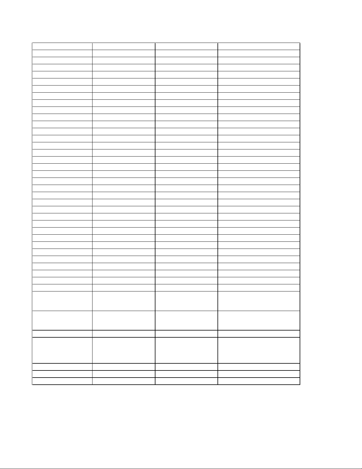
Pin Name (1) 208-Pin PQFP 240-Pin PQFP (2), (3) 256-Pin FineLine BGA
MSEL0 (4) 108 124 P1
MSEL1 (4) 107 123 R1
nSTATUS (4) 52 60 T16
nCONFIG (4) 105 121 N4
DCLK (4) 155 179 B2
CONF_DONE (4) 2 2 C15
INIT_DONE (5) 19 26 G16
nCE (4) 154 178 B1
nCEO (4) 3 3 B16
nWS (6) 206 238 B14
nRS (6) 204 236 C14
nCS (6) 208 240 A16
CS (6) 207 239 A15
RDYnBUSY (6) 16 23 G14
CLKUSR (6) 10 11 D15
DATA7 (6) 166 190 B5
DATA6 (6) 164 188 D4
DATA5 (6) 162 186 A4
DATA4 (6) 161 185 B4
DATA3 (6) 159 183 C3
DATA2 (6) 158 182 A2
DATA1 (6) 157 181 B3
DATA0 (4), (7) 156 180 A1
TDI (4) 153 177 C2
TDO (4) 4 4 C16
TCK (4) 1 1 B15
TMS (4) 50 58 P15
TRST (4) 51 59 R16
Dedicated Inputs 78, 80, 182, 184 90, 92, 210, 212 B9, E8, M9, R8
Dedicated Clock Pins 79, 183 91, 211 A9, L8
GCLK1 (8) 79 91 L8
Lock (9) 62 73 P12
DEV_CLRn (5) 180 209 D8
DEV_OE (5) 186 213 C9
VCCINT (2.5 V) 6, 23, 35, 43, 76, 106,
109, 117, 137, 145, 181
5, 27, 47, 96, 122, 130,
150, 170
E11, F5, F7, F9, F12, H6, H7,
H10, J7, J10, J11, K9, L5, L7,
L12, M11, R2
VCCIO (2.5 or 3.3 V) 5, 22, 34, 42, 66, 84, 98,
110, 118, 138, 146, 165,
178, 194
16, 37, 57, 77, 112, 140,
160, 189, 205, 224
D12, E6, F8, F10, G6, G8, G11,
H11, J6, K6, K8, K11, L10, M6,
N12
VCC_CKLK (10) 77 (11) 89 (11) L9 (9)
GNDINT 20, 21, 32, 33, 48, 49,
59, 72, 82, 91, 123, 124,
129, 130, 151, 152, 171,
185, 188, 201
10, 22, 32, 42, 52, 69,
85, 104, 125, 135, 145,
155, 165, 176, 197, 216,
232
E5, E12, F6, F11, G7, G9, G10,
H8, H9, J8, J9, K7, K10, L6, L11,
M5, M12
GNDIO – – –
GND_CKLK (10) 81 (12) 93 (12) T8 (10)
Total User I/O Pins (13) 147 189 191
ver. 1.0
Altera Corporation 1
Page 2

EPF10K100B Pin Table
y
y
Notes:
(1) All pins that are not listed are user I/O pins.
(2) EPF10K50E, EPF10K100E, and EPF10K100B devices are pin-compatible with EPF10K130E devices in
the same package if pins 20, 76, and 159 are connected to VCCINT. The MAX+PLUS II software
performs this function automaticall
(3) EPF10K50E, EPF10K100E, and EPF10K100B devices are pin-compatible with EPF10K200E devices in
the same package if pins 20, 40, 76, 139, 159, 187, and 225 are connected to VCCINT. The MAX+PLUS
II software performs this function automaticall
(4) This pin is a dedicated pin; it is not available as a user I/O pin.
(5)
This pin can be used as a user I/O pin if it is not used for its device-wide or configuration function.
(6)
This pin can be used as a user I/O pin after configuration.
(7) This pin is tri-stated in user mode.
(8) This pin drives the ClockLock and ClockBoost circuitry.
(9) This pin shows the status of the ClockLock and ClockBoost circuitry. When the ClockLock and
ClockBoost circuitry is locked to the incoming clock and generates an internal clock, LOCK is driven
high. LOCK remains high if a periodic clock stops clocking. The LOCK function is optional; if the LOCK
output is not used, this pin is a user I/O pin.
(10) This pin is the power or ground for the ClockLock and ClockBoost circuitry. To ensure noise resistance,
the power and ground supply to the Clock Lock and Clock Boost circuitry should be isolated from the
power and ground to the rest of the device. If the ClockLock or ClockBoost circuitry is not used, this
power or ground pin should be connected to VCCINT or GNDINT, respectively.
(11)
When using EPF10K100B devices, connect this pin to VCCINT.
(12)
When using EPF10K100B devices, connect this pin to GNDINT.
(13) The user I/O pin count includes dedicated inputs, dedicated clock inputs, and all I/O pins.
when future migration is set.
when future migration is set.
ver. 1.0
Altera Corporation 2
Page 3

Copyright © 1995, 1996, 1997, 1998, 1999 Altera Corporation, 101 Innovation Drive,
San Jose, CA 95134, USA, all rights reserved.
By accessing this information, you agree to be bound by the terms of Altera’s
Legal Notice.
 Loading...