

Page 1

Stratix II GX EP2SGX90 Transceiver
Signal Integrity Development Board
101 Innovation Drive
San Jose, CA 95134
(408) 544-7000
www.altera.com
Reference Manual
Development Board Version: 1.0.0
Document Version: 1.0.0
Document Date: May 2006
Page 2

Copyright © 2006 Altera Corporation. All rights reserved. Altera, The Programmable Solutions Company, the stylized Altera logo, specific device designations, and all other words and logos that are identified as trademarks and/or service marks are, unless noted otherwise, the trademarks and
service marks of Altera Corporation in the U.S. and other countries. All other product or service names are the property of their respective holders. Altera products are protected under numerous U.S. and foreign patents and pending applications, maskwork rights, and copyrights. Altera warrants
performance of its semiconductor products to current specifications in accordance with Altera's standard warranty, but reserves the right to make
changes to any products and services at any time without notice. Altera assumes no responsibility or liability arising out of the application or use of any information, product, or service described herein except as expressly agreed to in writing by Altera
Corporation. Altera customers are advised to obtain the latest version of device specifications before relying on any published information and before placing orders for products or services.
Part Number MNL-S2GXSIDB-1.0
ii Development Board Version 1.0.0 Altera Corporation
Stratix II GX EP2SGX90 Transceiver Signal Integrity Development Board Reference Manual May 2006
Page 3

Contents
About this Manual
Revision History ......................................................................................................................................... v
How to Contact Altera ............................................................................................................................... v
Typographic Conventions....................................................................................................................... vi
Chapter 1. Introduction
General Description................................................................................................................................ 1-1
Board Component Blocks................................................................................................................. 1-2
Block Diagram ................................................................................................................................... 1-3
Target Applications........................................................................................................................... 1-3
Data Rate & Clock Frequency Support Per Protocol ................................................................... 1-4
Handling the Board ................................................................................................................................ 1-4
Chapter 2. Board Components & Interfaces
Board Overview ...................................................................................................................................... 2-1
Featured Device ...................................................................................................................................... 2-6
Clocking Circuitry ................................................................................................................................. 2-7
Clock Buffer Functional Descriptions ............................................................................................ 2-9
ICS557-03 (U5): Spread Spectrum Clock Generator for PCI-Express ................................. 2-10
ICS8543 (U8): General Purpose 1:4 Differential Fanout Buffer ........................................... 2-11
ICS83023 (U7): Differential I/O to Single Converter for Trigger Clock ............................ 2-11
Interfaces ................................................................................................................................................ 2-12
SMA Connectors for High-Speed I/O ............................................................................................... 2-12
USB Interface ......................................................................................................................................... 2-14
General User Interfaces ........................................................................................................................ 2-16
Debug Header (J1) ........................................................................................................................... 2-16
LEDs (D1 Through D8) ................................................................................................................... 2-18
7-Segment Displays (D9, D10) ....................................................................................................... 2-19
Push-Button Switches (S1 Through S6) ........................................................................................ 2-21
DIP Switches (S7 and S8) ................................................................................................................ 2-22
Clock Selection Switches (S9 and S10) ......................................................................................... 2-24
Power Supply ....................................................................................................................................... 2-25
Thermal Management Block ............................................................................................................... 2-27
FPGA Configuration Block ................................................................................................................. 2-28
JTAG Configuration ........................................................................................................................ 2-28
Active Serial Configuration Using EPCS64 Device (U22) ......................................................... 2-28
Flash Memory ....................................................................................................................................... 2-30
Altera Corporation iii
May 2006 Preliminary
Page 4

Contents Stratix II GX EP2GX90 Signal Integrity Development Board Reference Manual
iv Altera Corporation
Preliminary May 2006
Page 5
About this Manual
Revision History
Chapter Date Version Changes Made
All May 2006 1.0.0 First publication
How to Contact Altera
Information Type USA & Canada All Other Locations
Technical support www.altera.com/mysupport/ www.altera.com/mysupport/
Product literature www.altera.com www.altera.com
Altera literature services literature@altera.com literature@altera.com
Non-technical customer
service
FTP site ftp.altera.com ftp.altera.com
The table below displays the revision history for the chapters in this
reference manual.
This reference manual provides comprehensive information about the
®
Altera
Stratix®II GX family of devices and the Stratix II GX EP2SGX90
transceiver signal integrity development board.
For the most up-to-date information about Altera products, go to the
Altera world-wide web site at www.altera.com. For technical support on
this product, go to www.altera.com/mysupport. For additional
information about Altera products, consult the sources shown below.
(800) 800-EPLD (3753)
(7:00 a.m. to 5:00 p.m. Pacific Time)
(800) 767-3753 + 1 408-544-7000
+1 408-544-8767
7:00 a.m. to 5:00 p.m. (GMT -8:00)
Pacific Time
7:00 a.m. to 5:00 p.m. (GMT -8:00)
Pacific Time
Altera Corporation v
May 2006 Preliminary
Page 6
Typographic Conventions Stratix II GX EP2GX90 Signal Integrity Development Board Reference Manual
Typographic
This document uses the typographic conventions shown below.
Conventions
Visual Cue Meaning
Bold Type with Initial
Capital Letters
bold type External timing parameters, directory names, project names, disk drive names,
Italic Type with Initial Capital
Letters
Italic type Internal timing parameters and variables are shown in italic type.
Initial Capital Letters Keyboard ke ys and menu names are shown with initial capital letters. Examples:
“Subheading Title” References to sections within a document and titles of on-line help topics are
Courier type Signal and port names are shown in lowercase Courier type. Examples: data1,
1., 2., 3., and
a., b., c., etc.
● • Bullets are used in a list of items when the sequence of the items is not important.
■
v The checkmark indicates a procedure that consists of one step only.
1 The hand points to information that requires special attention.
c
w
r The angled arrow indicates you should press the Enter key.
f The feet direct you to more information on a particular topic.
Command names, dialog box titles, chec kbox options, and dialog bo x options are
shown in bold, initial capital letters. Example: Save As dialog box.
filenames, filename extensions, and software utility names are shown in bold
type. Examples: f
Document titles are shown in italic type with initial capital letters. Example: AN 75:
High-Speed Board Design.
Examples: t
Variable names are enclosed in angle brackets (< >) and shown in italic type.
Example: <file name>, <project name>.pof file.
Delete key, the Options menu.
shown in quotation marks. Example: “Typographic Conventions.”
PIA
, \qdesigns directory, d: drive, chiptrip.gdf file.
MAX
, n + 1.
tdi, input. Active-low signals are denoted by suffix n, e.g., resetn.
Anything that must be typed exactly as it appears is shown in Courier type. For
example:
actual file, such as a Report File, references to parts of files (e.g., the AHDL
keyword
Courier.
Numbered steps are used in a list of items when the sequence of the items is
important, such as the steps listed in a procedure.
The caution indicates required information that needs special consideration and
understanding and should be read prior to starting or continuing with the
procedure or process.
The warning indicates information that should be read prior to starting or
continuing the procedure or processes
c:\qdesigns\tutorial\chiptrip.gdf. Also, sections of an
SUBDESIGN), as well as logic function names (e.g., TRI) are shown in
vi Altera Corporation
Preliminary May 2006
Page 7

1. Introduction
General Description
The Stratix®II GX EP2SGX90 transceiver signal integrity development
board provides a hardware platform for developing and prototyping
high-speed designs using power-efficient Stratix II GX devices. The
transceiver technology embedded in Stratix II GX devices ensures that
signal integrity extends to high frequencies while also providing a
power-efficient, single-chip solution that supports the following
high-speed serial protocols:
■ PCI-Express
■ CEI-6G
■ Gigabit Ethernet
■ XAUI
■ Serial RapidIO
■ SONET Backplane
■ SDI
■ SerialLite II
As board designs move into the Gbps space, it is increasingly more
difficult to maintain signal integrity. In fact, increasing data rates for both
I/O interfaces and memory interfaces can present significant data
transmission problems and performance issues.
The Stratix II GX device’s embedded transceivers provide enhanced
transmit pre-emphasis technology that conditions the signal prior to
transmission as well as programmable receiver equalization circuitry.
Also, because the Stratix II GX device’s embedded transceivers have
built-in clock data recovery, you do not have to route the clock and data
on the board, which greatly simplifies high-speed board designs.
™
®
To further simplify the process, Altera
use as either a design starting point or an experimental platform. The
reference design is designed and tested by Altera engineers and
distributed with the Transceiver SI Development Kit, Stratix II GX
Edition (ordering code: DK-SI-2SGX90N).
Altera Corporation Reference Manual 1–1
May 2006 Preliminary
provides a reference design for
Page 8

General Description
Board Component Blocks
The board provides the following major component blocks:
■ Flexible clock management system
● Four high-speed clock oscillators to support a variety of
protocols:
• 156.25 MHz
• 25, 100, 125, and 200-MHz from the clock generator
• 50 MHz
● SMA connectors for clock input and output
■ High-speed I/O & SMA connectors
● SMA connectors for high-speed interfaces
● Six channels of transmit differential output and six channels of
receive differential input at up to 6.375 Gbps
■ Power-supply management
● 5-V, 3.3-V, and 1.2-V switching regulators
● 3.3-V and 1.5-V/1.2-V linear regulators
■ USB interface
● Operates like a COM port on a host PC
● Eliminates the need for:
• Full USB software and hardware implementation
• USB software driver
■ General user-interface
● Debugging header
● LEDs
● 7-Segment LEDs
● Push-buttons
● DIP switches
■ Thermal management
■ Flash memory
● 56-pin TSOP package
● Compliant with common Flash interface (CFI)
● Reduces development time when used with the Altera SOPC
Builder CFI controller module
■ FPGA configuration
● JTAG interface header
● Active serial configuration scheme using EPCS64 device
• Configures Stratix II GX device on power-up
1–2 Reference Manual Altera Corporation
Stratix II GX EP2SGX90 Transceiver Signal Integrity Development Board May 2006
Page 9
Introduction
e
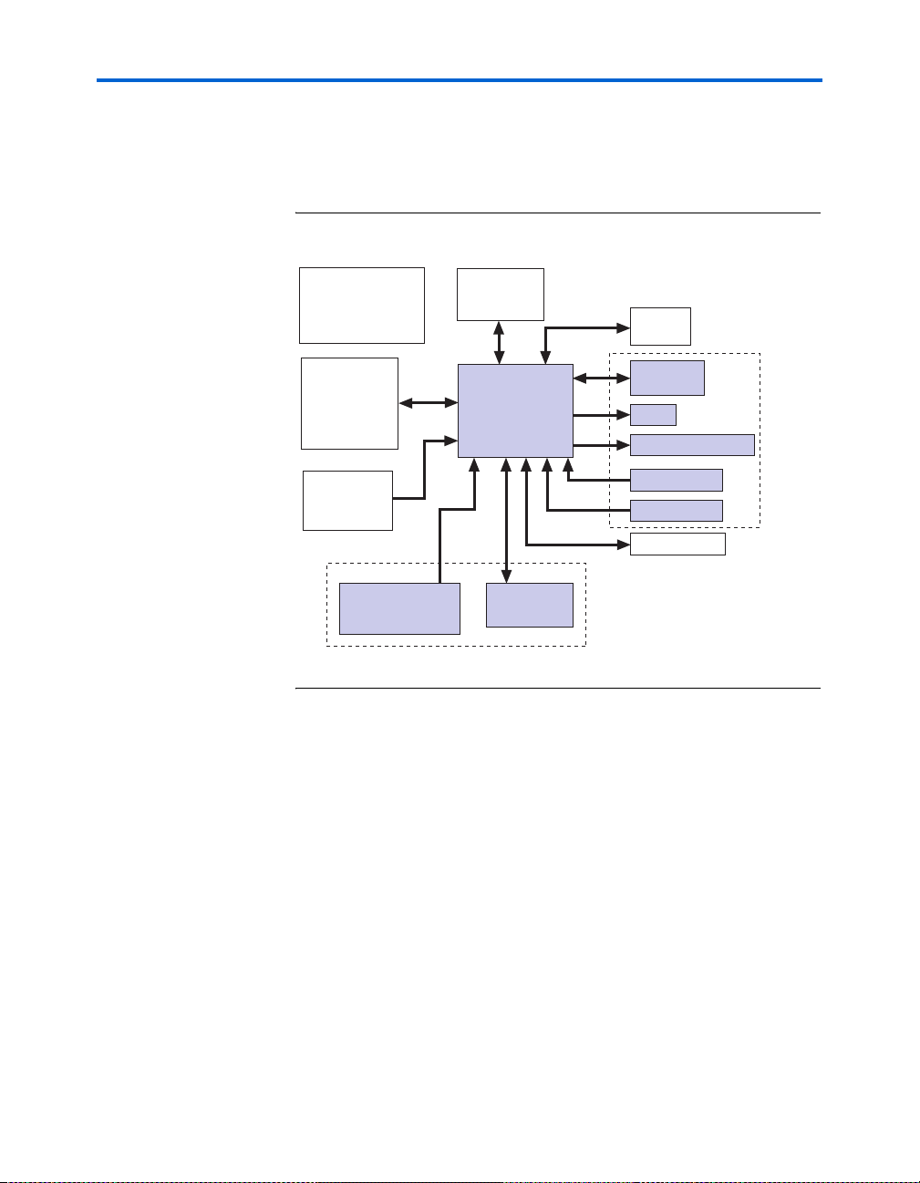
Block Diagram
Figure 1–1 shows a functional block diagram of the Stratix II GX
EP2SGX90 transceiver signal integrity development board.
Figure 1–1. Stratix II GX EP2SGX90 Transceiver Signal Integrity Development
Board Block Diagram
Power Supply
Management Block
with Switching &
Linear Regulators
Clock
Management
Unit
USB
Interface
SMA
Connectors
for High-Speed
Interfaces
Thermal
Management
Block
Active Serial
Configuration Using
EPCS64 Device
Stratix II GX
Device
JTAG
Configuration
Debugging
Header
LEDs
7-Segment Displays
Push Buttons
DIP Switches
Flash Memory
FPGA
Configuation
Block
General
User
Interfac
Block
Target Applications
The board is used for the following applications:
■ Demonstrating key StratixIIGX device features
■ Device qualification, e.g., jitter, pre-emphasis, equalization, and
signal integrity testing, as well as receiver sensitivity.
■ De-coupling Quartus
Altera MegaWizard
devices and interfaces included)
■ Demonstrating Stratix II GX device transceiver features
■ Characterization testing of high-speed serial interfaces
■ Interoperability testing between various devices via on-board SMA
connectors
■ Power supply evaluation (on-board regulation and banana jack
options)
®
II software, transceiver architecture, and
®
Plug-In Manager demonstrations (supporting
Altera Corporation Reference Manual 1–3
May 2006 Stratix II GX EP2SGX90 Transceiver Signal Integrity Development Board
Page 10
Handling the Board
■ Clocking evaluation to qualify the Stratix II GX device with user
clock sources
■ Demonstrate signal integrity features on a standalone basis
Data Rate & Clock Frequency Support Per Protocol
Table 1–1 shows the board’s data rate and clock frequency support per
protocol.
Table 1–1. Board Protocol Support
Handling the
Board
Protocol
6G - CEI 6.25 156.25 On board oscillator
5G scrambled 5 156.25 On board oscillator
4G FC, (1) 4.25 – SMA clock input
XAUI 3.125 156.25 On board oscillator
PCI-Express/PIPE 2.5 100 On board oscillator
SONET backplane 2.488 – SMA clock input
2G FC, (1) 2.125 – SMA clock input
HD - SDI 1.485 – SMA clock input
GIGE 1.25 125 On board oscillator
1G FC, (1) 1.063 – SMA clock input
Note to Ta b l e 1 – 1:
(1) There is no support planned for Fibre channel protocol. This table only shows
supported data rate.
Data Rate
(Gbps)
Clock
Frequency
(MHz)
Clock Source
When handling the board, it is important to observe the following
precaution:
w Static Discharge Precaution—Without proper anti-static
handling, the board can be damaged. Therefore, use anti-static
handling precautions when touching the board.
1–4 Reference Manual Altera Corporation
Stratix II GX EP2SGX90 Transceiver Signal Integrity Development Board May 2006
Page 11

2. Board Components & Interfaces
Board Overview
f For information on powering-up the Stratix II GX transceiver signal
This chapter provides operational and connectivity detail for the board’s
major components and interfaces and is divided into the following major
blocks:
■ Featured device
■ Clocking circuitry
■ Interfaces
● SMA connectors for high-speed I/O
● USB interface
● General user interfaces
■ Power supply
■ Thermal management
■ FPGA configuration
■ Flash memory
1 Board schematics, the physical layout database, and
®
manufacturing files for the Stratix
II GX EP2SGX90 transceiver
signal integrity development board are included in the
Transceiver SI Development Kit, Stratix II GX Edition in the
following directory:
<install path>\SIIGX_SI_Kit-v1.0.0\Docs\BoardDesignFiles
integrity development board and installing the demo software, refer to
the Transceiver SI Development Kit, Stratix II GX Edition Getting Started
User Guide.
Altera Corporation Reference Manual 2–1
May 2006 Preliminary
Page 12
Board Overview
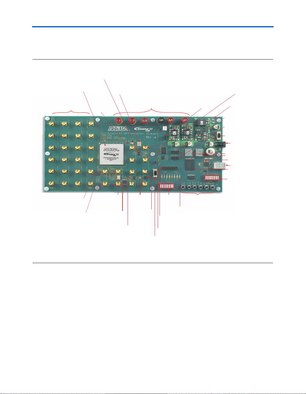
Figure 2–1 shows the top view of the Stratix II GX EP2SGX90 transceiver
signal integrity development board.
Figure 2–1. Top View of the Stratix II GX EP2SGX90 Transceiver Signal Integrity Development Board
Temperature Sensor
with Alarm (U17)
Stratix II GX Device (U20)
SMA Transmit &
Receive Connectors
(J26 through J49)
SMA Output Clock Connectors
Reference Clock for Quad 1
Transceivers (J7, J8)
SMA Output Clock Connectors
Reference Clock for Quad 3
Transceivers (J9, J10)
Configuration
Done LED (D14)
156.25-MHz
Oscillator (U9)
50-MHz Oscillator
Used for System Clock (U10)
Optional Power Input
Connection Jacks (J15, J17-21)
25-MHz
Crystal (U6)
Differential
Fan-out
Buffer (U8)
Differential to
Single-Ended
Buffer (U7)
Clock
Generator (U5)
Switch (S9)
Clock
Setting
DIP Switch
Bank (S8)
Debug
Header (J1)
EPCS64 Device (U22)
Slide
Connectors for FPGA (J12, J14)
Jumper Header for
VCCH Voltage (J50)
User Push-Button
Switches (S1 through S6)
User LEDs
(D1 through D8)
SMA Input Clock
Power LED (D13)
10-pin Configuration Header
for EPCS64 Device (J23)
10-pin JTAG Configuration
Header for FPGA (J24)
Power Switch (S10)
Power Supply Input
Dual 7-Segment
Displays (D9, D10)
USB Interface (U2)
USB Connector (J2)
16 Mbytes Flash
Memory (U19)
User DIP Switch
Bank (S7)
2–2 Reference Manual Altera Corporation
Stratix II GX EP2SGX90 Transceiver Signal Integrity Development Board May 2006
Page 13

Board Components & Interfaces
Figure 2–2 shows the diagonal view of the Stratix II GX EP2SGX90
transceiver signal integrity development board.
Figure 2–2. Diagonal View of the Stratix II GX EP2SGX90 Transceiver Signal Integrity Development Board
Altera Corporation Reference Manual 2–3
May 2006 Stratix II GX EP2SGX90 Transceiver Signal Integrity Development Board
Page 14

Board Overview
Table 2–1 describes the components and lists their corresponding board
references.
Table 2–1. Stratix II GX Transceiver SI Development Board Components & Interfaces (Part 1 of 3)
Typ e
Featured
Device
FPGA Stratix II GX
User
Interfaces
I/O Push-button
I/O DIP switch S7 Eight toggle DIP switches for user-defined, logic inputs. 2–22
I/O LEDs D1-D8 Eight user-defined LEDs 2–18
I/O Dual seven-
I/O Slide switch S9 Double-pole, single-throw slide switch for selecting
I/O DIP switch S8 Eight toggle DIP switches for selecting PCIe clock speed,
Debugging Interfaces
I/O Debug header J1 A twenty-pin connector that is connected to 20 general I/Os
Connections & Interfaces
I/O USB UART U2, J2 USB interface to the Stratix II GX device for device
I/O SMA transmit
Configuration & Reset
Input Connector J23 Header for programming the EPCS64 serial configuration
Input Connector J24 Header for configuring the Stratix II GX device. 2–28
Input Jumper
Component/
Interface
device
switches
segment
display
and receive
connectors
header
Board
Reference
U20 EP2SGX90EF1152C3NES or EP2SGX90EF35C3NES 2–6
S1-S6 Six push-button switches for user-defined, logic inputs. 2–21
D9, D10 Dual seven-segment display 2–19
between the 156.25 MHZ oscillator and the SMA external
clock inputs to supply the clocks to the three quad
transceivers.
PCIe clock spread-spectrum setting, and the output enable
of the clocks to the three quad transceivers.
on the FPGA.
configuration and communication with applications running
on the device.
J26-J49 SMA connectors with the transmit and receive signals from
the quad transceivers
device.
J25 Jumper header to select which JTAG source the board
uses, i.e., the JTAG header configuration or the USB JT A G
configuration.
Description Page
2–24
2–22
2–16
2–14
2–12
2–28
2–28
2–4 Reference Manual Altera Corporation
Stratix II GX EP2SGX90 Transceiver Signal Integrity Development Board May 2006
Page 15

Board Components & Interfaces
Table 2–1. Stratix II GX Transceiver SI Development Board Components & Interfaces (Part 2 of 3)
Typ e
Display Configuration
Memory
Flash 16 Mbytes of
Serial flash 64 Mbits of
Clock Circuitry
Crystal Clock U6 Crystal 25MHz 2–7
Clock
Generator
Oscillator Clock U9 156.25-MHZ oscillator 2–7
Buffer Clock U8 1:4 differential fan-out buffer 2–9
Buffer Clock U7 Differential to single-ended converter for providing trigger
Input SMA external
Output SMA trigger
Output SMA trigger
Oscillator Clock U10 50-MHz clock oscillator used for the system clock. 2–7
Input SMA input
Input SMA input
Output SMA output
Component/
Interface
done LED
flash memory
serial flash
memory
Clock U5 Spread spectrum clock generator for 25-MHz, 100-MHz,
clock input
connectors
clock
connector
clock
connector
clock
connectors
clock
connectors
clock
connectors
Board
Reference
D14 LED that illuminates upon successful FPGA configuration. 2–28
U19 16 Mbytes of non-volatile memory. 2–30
U22
J5, J6 SMA connectors for providing an external clock to the three
J3 SMA connector for the PCIe trigger clock. 2–12
J4 SMA connector for the basic trigger clock associated with
J7, J8 Reference clock input for quad 1 transceiver 2–12
J9, J10 Reference clock input for quad 3 transceiver 2–12
J12, J14 Output clock from Stratix II GX 2–12
®
Altera
EPCS64 low-cost serial configuration device to
configure the Stratix II GX device
125-MHz, and 200-MHz clocks.
clocks.
quad transceivers.
the three quad transceivers.
Description Page
2–28
2–10
2–9
2–12
2–12
Altera Corporation Reference Manual 2–5
May 2006 Stratix II GX EP2SGX90 Transceiver Signal Integrity Development Board
Page 16

Featured Device
Table 2–1. Stratix II GX Transceiver SI Development Board Components & Interfaces (Part 3 of 3)
Typ e
Power Supp ly
Input DC power
Input Power switch S10 Switches the board’s power on and off. 2–25
Input Optional
Input Jumper
Output Temperature
Component/
Interface
jack
power input
connection
jacks
header
sensor
Featured
Device
Board
Reference
J16 16-V DC unregulated power source. 2–25
J17, J15,
J18, J19,
J20, J21
J50 Jumper header for selecting between 1.5-V DC and
U17 Performs thermal management, i.e., turning the cooling fan
External power supply can be connected for high current
applications.
1.2-V DC supplied to the quad transceivers. Jumper pins 1
and 2 select 1.5-V output, and jumper pins 2 and 3 select
1.2-V output.
on and off to regulate the FPGA temperature.
Description Page
2–25
2–25
2–25
The Transceiver SI Development Kit, Stratix II GX Edition features the
®
EP2SGX90EF1152 FPGA (U20) in a 1152-pin FineLine BGA
(FBGA)
package. Table 2–2 lists some Stratix II GX device features.
Table 2–2. Stratix II GX Features
Architectural
Feature
Altera’s thirdgeneration FPGA
with embedded
transceivers
Innovative clock
management
system
Based on the
1.2-V, 90-nm
SRAM process
● Provides a robust design solution for the most popular high-speed serial interfaces
● Provides optimum jitter performance across the entire operating range of 622 Mbps to
6.375 Gbps
● Provides best-in class signal integrity performance
● Offers enhanced transmit pre-emphasis technology, programmable receiver
equalization, and output voltage control
● Clock signals are automatically routed to the appropriate destination
● Greatly simplifies high-speed board designs
● Internal clock frequency of up to 500 MHz
● Provides up to 6.7 Mbits of on-chip TriMatrix
● Provides up to 63 DSP blocks for efficient implementation of high-performance filters
and other DSP functions
● Supports a wide range of external memory interfaces
Results
™
memory
f For additional information about Altera devices, go to
www.altera.com/products/devices.
2–6 Reference Manual Altera Corporation
Stratix II GX EP2SGX90 Transceiver Signal Integrity Development Board May 2006
Page 17

Board Components & Interfaces
You can configure the Stratix II GX device in one of two ways:
■ Active serial configuration via the EPCS64 device
■ JTAG configuration
Clocking Circuitry
The Stratix II GX transceiver signal integrity development board’s
clocking circuitry is designed to be flexible and easy to use. In fact, with
the Stratix II GX device’s embedded transceivers, you do not need to
route the board’s clock and data signals. Instead, the embedded
transceivers route the clock and data signals to the appropriate
destination.
The Stratix II GX devices have dedicated phase-locked loops (PLLs) for
high-speed transceivers, enhanced PLLs for spread-spectrum and general
purpose clocking, and fast PLLs for high-speed differential I/O clocking,
which support the high-speed interfaces described in this chapter. See
Figure 2–3.
The clocking block is comprised of:
■ High-speed clock oscillators:
• 156.25-MHz oscillator
• 50-MHz oscillator
■ 25 MHz crystal
■ SMA connectors for clocking input and output signals
Table 2–3 lists the board’s clocking parts list.
Table 2–3. Clocking Block Parts List
Part Name
ICS557-03 1 U5 Spread spectrum PLL
ICS8543 1 U8 Clock buffer to input
ICS830231 1 U7 Clock buffer differential to
SMA connectors 12 J3 - J14 High-speed interface support
25-MHz crystal 1 U6 Supports the ICS557-03 clock
156.25-MHz oscillator 1 U9 Supports the OIF, CEI-6G, and
50-MHz oscillator 1 U10 Supports the ICS8543 clock
Number of
Units
Board
Reference
Purpose
multiplexer to 4 LVDS outputs
single-ended converter
buffer
XAUI protocols
buffer
Altera Corporation Reference Manual 2–7
May 2006 Stratix II GX EP2SGX90 Transceiver Signal Integrity Development Board
Page 18

Clocking Circuitry
Table 2–4 lists the clocking circuitry’s board references, speeds, interface
support, and manufacturing information.
Table 2–4. Board Clocking Circuitry
Board
Reference
U9 156.25 MHz XAUI
U5 25, 100,
U7 25 MHz Differential
U8 50 MHz General
Speed I/O Support Manufacturing Information Additional Information
CEI-6G
PCI-Express
125, and
200 MHz
GbE
I/O to
single-ended
buffer
purpose
clocking
SMD package, 3.3V, low-voltage
positive emitter coupled logic
(LVPECL) output
16-pin TSSOP package, 3.3V, and
high-speed current steering logic
(HCSL) output
Part # ICS557-03
Small outline integrated circuit
(SOIC) 8-pin package, 3.3V, and
LVDS/LVPECL/HCSL input and
LVCOMS output
Part # ICS83023
20-pin TSSOP package,
3.3V, LVPECL/LVDS input and
LVDS output
Part # ICS8543
Supports the OIF, CEI-6G, and
XAUI protocols.
Spread-spectrum clock
generator for PCIe clocks.
The integrated circuit system’s
(ICS) PLL uses a 25 MHz crystal
input and produces two pairs of
differential outputs at 25-MHz,
100-MHz, 125-MHz, and
200-MHz clock frequencies. The
PLL also provides spread
selection of ±25%, -0.5%,
-0.75%, and no spread.
Differential I/O to LVCMOS
translator.
A 2:1 multiplexer to a 4:1
low-voltage differential signaling
(LVDS) fanout buffer.
2–8 Reference Manual Altera Corporation
Stratix II GX EP2SGX90 Transceiver Signal Integrity Development Board May 2006
Page 19

Figure 2–3 shows the clock signals passing through logic translators and
automatically routing to the appropriate destination.
Figure 2–3. Clocking Circuitry Automatic Routing Paths
Spread Spectrum
Clock Generator for PCI-Express (U5)
25 MHz
Oscillator
General Purpose
Clocking Buffer:
2:1 Multiplexer
to a 1:4 LVDS
Fanout
Buffer (U8)
SMA Connector Clock
Input (P = J5, N = J6)
156 MHz
Oscillator
ICS557-03
ICS8543
Differential I/O to
LVCMOS Translator (U7)
ICS83023
Board Components & Interfaces
refclk0 in Quad2
PCI-Express Trigger Clock (J3)
Basic Trigger Clock (J4)
refclk1 in Quad1
refclk1 in Quad2
refclk1 in Quad3
50 MHz
Oscillator
SMA
Connector
Clock Input
(P= J12, N = J14)
Global Clock for FPGA Block
Global Clock for FPGA Block
Output Clock
from FPGA Side
(P = J11, N = J13)
= LVPECL/LVDS Input
= HCSL Output
= LVDS Output
refclk0 in Quad1
(P = J7, N = J8)
refclk0 in Quad3
(P = J9, N = J10)
Clock Buffer Functional Descriptions
This section provides functional descriptions for the board’s three clock
buffers:
■ ICS557-03 (U5)
■ ICS8543 (U8)
■ ICS83023 (U7)
Altera Corporation Reference Manual 2–9
May 2006 Stratix II GX EP2SGX90 Transceiver Signal Integrity Development Board
Page 20

Clocking Circuitry
ICS557-03 (U5): Spread Spectrum Clock Generator for PCI-Express
The ICS557-03 is a spread spectrum clock generator supporting PCIe and
Ethernet protocol requirements. The device is used to substantially
reduce electromagnetic interference (EMI) in PC or embedded systems.
The device provides two differential spread spectrum outputs, and is pinconfigured for clock and spread selection. Using phase-locked loop (PLL)
techniques, the device takes a 25 MHz crystal input and produces two
pairs of differential outputs (HCSL) at 25 MHz, 100 MHz, 125 MHz and
200 MHz clock frequencies. The device also provides spread selection of
±0.25%, -0.5%, -0.75%, and no spread.
Table 2–5 lists output clock DIP switch settings.
Table 2–5. Output Clock Setting DIP Switch Pinout (S8)
Switch 25 MHz 100 MHz 125 MHz 200 MHz
SW1 Closed Open Closed Open
SW2 Closed Closed Open Open
Table 2–6 lists spread spectrum output selection DIP switch settings.
Table 2–6. Spread Spectrum Output Selection Setting (S8)
Switch Center =/-0.25 Down -0.5 Down -0.75 No Spread
SW3 Closed Open Closed Open
SW4 Closed Closed Open Open
2–10 Reference Manual Altera Corporation
Stratix II GX EP2SGX90 Transceiver Signal Integrity Development Board May 2006
Page 21

Board Components & Interfaces
ICS8543 (U8): General Purpose 1:4 Differential Fanout Buffer
The ICS8543 is a general purpose clock buffer with a 2:1 multiplexer input
and a 1:4 differential fanout. The clk_sel signal determines which clock
input (i.e., clk or pclk) is used; the chosen signal is then converted to
four output clocks. See Figure 2–4.
Figure 2–4. ICS8543 Clock Buffer Block Diagram
clk_en
clk
nclk
pclk
npclk
clk_sel
oe
0
1
D
LE
Q
Q0
nQ0
Q1
nQ1
Q2
nQ2
Q3
nQ3
ICS83023 (U7): Differential I/O to Single Converter for Trigger Clock
The ICS83023 is a differential I/O to a single-ended clock buffer, which is
used for both the PCI-Express and Basic trigger clocks. See Figure 2–5.
Figure 2–5. ICS83023 Clock Buffer Block Diagram
clk0
nclk0
clk1
nclk1
Q0
Q1
Altera Corporation Reference Manual 2–11
May 2006 Stratix II GX EP2SGX90 Transceiver Signal Integrity Development Board
Page 22

Interfaces
Interfaces
This section describes the Stratix II GX EPS2GX90 transceiver signal
integrity development board’s interface architecture. There are three
main interface blocks:
■ SMA connectors for high-speed I/O
■ USB interface
■ General user interfaces
SMA Connectors for High-Speed I/O
The Stratix II GX EPS2GX90 transceiver signal integrity development
board has SMA connectors supporting the most commonly-used, highspeed interface protocols. The SMA connectors are helpful for equipment
testing. The board has six channels of transmit (TX) differential output as
well as six channels of receive (RX) differential input running at up to
6.375 Gbps. See Figure 2–6.
Table 2–7 lists the SMA-to-FPGA pinout table.
Table 2–7. SMA-to-FPGA Pinout Table
SMA Board
Reference
J7
J8
J9
J10
J11
J12
J13
J14
Schematic Signal Name
REFCLKOP_QUAD1
REFCLKON_QUAD1
REFCLKOP_QUAD3
REFCLKON_QUAD3
CLOCKOUT_P
GLK_P
CLOCKOUT_N
GCLK_N
Stratix II GX (U20)
Pin Number
G1
G2
AK4
AK5
AP17
AP18
AN17
AP19
2–12 Reference Manual Altera Corporation
Stratix II GX EP2SGX90 Transceiver Signal Integrity Development Board May 2006
Page 23

Figure 2–6. SMA Connector Block Diagram
Transceiver Block 1
1 Channel
Stratix II GX Device
Transceiver Block
Board Components & Interfaces
SMA Connectors
(J27, J28)
(J29, J26)
(J43, J45)
(J42, J44)
(J39, J40)
Transceiver Block 2
4 Channels
Transceiver Block 3
1 Channel
(J32, 33)
(J36, J37)
(J47, J48)
TX: 40 inch trace length
(J38, J41)
(J30, J31)
(J34, 35)
(J49, J46)
Table 2–8 lists transceiver block’s transmit and receive signals,
corresponding SMA reference designators and FPGA pins.
Table 2–8. Transceiver Block Corresponding Signals, SMA Designator, and
FPGA Pin (Part 1 of 2)
Block Signal
Transceiver Block 1,
1 Channel
TX_P0 J27 A4
TX_N0 J28 A5
RX_P0 J29 C1
RX_N0 J26 C2
SMA Reference
Designator
Stratix II GX Pin
Altera Corporation Reference Manual 2–13
May 2006 Stratix II GX EP2SGX90 Transceiver Signal Integrity Development Board
Page 24

Interfaces
Table 2–8. Transceiver Block Corresponding Signals, SMA Designator, and
FPGA Pin (Part 2 of 2)
Block Signal
Transceiver Block 2,
4 Channels
Transceiver Block 3,
1 Channel
SMA Reference
Designator
TX_P4 J43 AB4
TX_N4 J45 AB5
RX_P4 J42 AB1
RX_N4 J44 AB2
TX_P3 J39 Y4
TX_N3 J40 Y5
RX_P3 J38 Y1
RX_N3 J41 Y2
TX_P2 J32 N4
TX_N2 J33 N5
RX_P2 J30 N1
RX_N2 J31 N2
TX_P1 J36 R4
TX_N1 J37 R5
RX_P1 J34 R1
RX_N1 J35 R2
TX_P5 J47 AF4
TX_N5 J48 AF5
RX_P5 J49 AF1
RX_N5 J46 AF2
Stratix II GX Pin
USB Interface
The USB interface to the board provides a communication port to a host
PC. A USB physical connection is used to enable laptops without RS232
ports to communicate with the demo board.
To simplify the USB interface, the board contains a FTDI FT2232L USB
universal asynchronous receiver/transmitter (UART) circuit. The UART
eliminates the need for full USB software and hardware implementation.
In addition, the USB UART design allows the software to be designed as
if writing directly to the host PC’s COM port, which eliminates the need
for designing a USB software driver (see Figure 2–7).
2–14 Reference Manual Altera Corporation
Stratix II GX EP2SGX90 Transceiver Signal Integrity Development Board May 2006
Page 25

Board Components & Interfaces
Also, the 1 M Baud rate should be sufficient for the intended
communication applications. The FTDI circuit also has a downloadable
non-license USB direct driver and SLL software interface that configures
the USB connection into the host PC’s COM port.
Figure 2–7. USB Interface to Stratix II GX Transceiver Signal Integrity
Development Board
USB PHY
Connector
FT2232L
USB UART
Table 2–9 lists the USB interface to FPGA pinout.
Table 2–9. USB Interface to FPGA Pinout Table
USB Interface (U2)
Pin Number
40
39
38
37
36
35
33
32
30
29
28
27
Schematic Signal Name
UART_DATA0
UART_DATA1
UART_DATA2
UART_DATA3
UART_DATA4
UART_DATA5
UART_DATA6
UART_DATA7
UART_DATA8
UART_DATA9
UART_DATA10
UART_DATA11
Stratix II GX
Device
Stratix II GX (U20)
Pin Number
F30
G31
D33
D32
H29
G30
E32
E31
J28
K27
E34
D34
Altera Corporation Reference Manual 2–15
May 2006 Stratix II GX EP2SGX90 Transceiver Signal Integrity Development Board
Page 26

Interfaces
General User Interfaces
To allow you to fully leverage the I/O capabilities of the Stratix II GX
device for debugging, control, and monitoring purposes, the following
general user interfaces are available on the board:
■ Debug Header
■ LEDs
■ 7-segment display
■ LCD interface
■ Push buttons
■ DIP switches
Debug Header (J1)
Board reference J1 is a simple 20-pin debug header connected to the
Stratix II GX device’s general user I/O. The form factor is a dual row
header such as a FCI 20-pin header (Samtec TSW-110-07-G-D). Table 2–10
lists the schematic signal name and the corresponding Stratix II GX
device pin number.
Table 2–10. Debug Header Pin-Out (Part 1 of 2)
Header Number Schematic Signal Name
1 D_HED0 AB30
2 D_HED1 AA23
3 D_HED2 AB23
4 D_HED3 AB33
5 D_HED4 AB32
6 D_HED5 AA26
7 D_HED6 AA25
8 D_HED7 AA34
9 D_HED8 AB34
10 D_HED9 AB29
11 D_HED10 AB28
12 D_HED11 AC32
13 D_HED12 AC31
14 D_HED13 AB24
15 D_HED14 AC24
16 D_HED15 AC34
17 D_HED16 AC33
2–16 Reference Manual Altera Corporation
Stratix II GX EP2SGX90 Transceiver Signal Integrity Development Board May 2006
Stratix II GX (U20)
Pin Number
Page 27

Board Components & Interfaces
Table 2–10. Debug Header Pin-Out (Part 2 of 2)
Header Number Schematic Signal Name
18 D_HED17 AB26
19 D_HED18 AB25
20 D_HED19 AD32
Figure 2–8 shows the debug header’s schematic.
Figure 2–8. Debug Header (J1) Schematic
J1
D_HED0
D_HED2
D_HED4
D_HED6
D_HED8
D_HED10
D_HED12
D_HED14
D_HED16
D_HED18
1
3
5
7
Debug
9
Header
11
13
15
17
19
CONN_PCB_10X2
10
12
14
16
18
20
D_HED1
2
D_HED3
4
D_HED5
6
D_HED7
8
D_HED9
D_HED11
D_HED13
D_HED15
D_HED17
D_HED19
Stratix II GX (U20)
Pin Number
Figure 2–9 shows the debug header’s board labels.
Figure 2–9. Debug Header (J1) Board Labels
Altera Corporation Reference Manual 2–17
May 2006 Stratix II GX EP2SGX90 Transceiver Signal Integrity Development Board
Page 28

Interfaces
LEDs (D1 Through D8)
The board provides eight user-defined LEDs. D1 through D8 are
connected to general purpose I/O pins on the Stratix II GX EPS2GX90
device. When the EP2SGX90 device drives logic 0, the corresponding LED
illuminates. Table 2–11 lists the schematic signal name and the
corresponding Stratix II GX device’s pin number.
Table 2–11. User-Defined LED Pin-Out
Board
Reference
D1
D2
D3
D4
D5
D6
D7
D8
Schematic Signal Name
USER_LED0
USER_LED1
USER_LED2
USER_LED3
USER_LED4
USER_LED5
USER_LED6
USER_LED7
Stratix II GX (U20)
Pin Number
AE33
AE32
AD26
AD25
AD34
AE34
AC29
AC28
Figure 2–10 shows a board image of the user-defined LEDs.
Figure 2–10. User-Defined LEDs
2–18 Reference Manual Altera Corporation
Stratix II GX EP2SGX90 Transceiver Signal Integrity Development Board May 2006
Page 29

Figure 2–11 shows the LED schematic.
Figure 2–11. LED Schematic
3V3
D1
12
12
12
12
12
12
12
LED GREEN
D2
LED GREEN
D3
LED GREEN
D4
LED GREEN
D5
LED GREEN
D6
LED GREEN
D7
LED GREEN
Board Components & Interfaces
RN2
R_PACK-4
1
2
3
4
1
2
3
4
7
7
6
5
RN3 R_PACK-4
7
7
6
5
220Ω
USER_LED0
USER_LED2
USER_LED3
USER_LED4
USER_LED5
USER_LED6
USER_LED7
USER_LED8
D8
12
LED GREEN
7-Segment Displays (D9, D10)
Board references D9 and D10 are dual user-defined, seven-segment
displays. The primary function of the 7-segment displays is to display the
board’s hardware version, which simplifies board revision control.
To save board space, the 7-segment displays are a small form factor. Each
segment is individually controlled by a general purpose I/O pin. When
the EP2SGX90 FPGA pin drives logic 0, the corresponding segment
illuminates. See Figure 2–12.
Altera Corporation Reference Manual 2–19
May 2006 Stratix II GX EP2SGX90 Transceiver Signal Integrity Development Board
Page 30

Interfaces
P
Table 2–12 lists the 7-segment display pinouts.
Table 2–12. 7-Segment Display Pin-Outs
Board Reference D9 Board Reference D10
Segment
Display Name
A
B
C
D
E
F
G
DP
Schematic
Signal Name
DIG_1_A W31
DIG_1_B W30
DIG_1_C V23
DIG_1_D W23
DIG_1_E W33
DIG_1_F W32
DIG_1_G Y24
DIG_1_DP Y23
Stratix II GX
Pin Name
Figure 2–12 shows the board image and name of each segment.
Figure 2–12. Segment Names for the Dual 7-Segment Displays
Segment
Display Name
A
B
C
D
E
F
G
DP
D9
A
F
B
G
Schematic
Signal Name
DIG_2_A Y32
DIG_2_B Y31
DIG_2_C W28
DIG_2_D Y29
DIG_2_E Y34
DIG_2_F Y33
DIG_2_G Y28
DIG_2_DP Y27
D10
A
F
B
G
Stratix II GX
Pin Name
CE
D
2–20 Reference Manual Altera Corporation
Stratix II GX EP2SGX90 Transceiver Signal Integrity Development Board May 2006
DP
CE
D
D
Page 31

Board Components & Interfaces
Push-Button Switches (S1 Through S6)
Board references S1 through S6 are push-button switches allowing
general user I/O interfaces to the Stratix II GX device.
S1-S6 are user-defined, momentary-contact push-button switches used to
provide stimulus to a user design on the board. Each push-button is
connected through debounce circuitry to a Stratix II GX general-purpose
I/O pin as listed in Table 2–13. When the switch is pressed and held
down, the device pin is set to logic 0, when the switch is released, the
device pin is set to logic 1.
The push button device is a small form factor switch similar to the
Panasonic Tactile Switches (EVQPAC07K). Table 2–13 provides
operational descriptions and schematic signal names.
Table 2–13. Push-Button Switches (S1 Through S6)
Push-Button
Name
PB0 S1 PB0_IN AD28
PB1 S2 PB1_IN AF34
PB2 S3 PB2_IN AF33
PB3 S4 PB3_IN AF30
PB4 S5 PB4_IN AF29
Note to Table 2–13:
(1) The PB5 is a special purpose button, called DEV_CLRn, connected to the AH20 pin
of the FPGA. The PB5 clears the FPGA data.
Board
Reference
Designator
Schematic Signal
Name
Stratix II GX Device
(U20) Pin Number
Altera Corporation Reference Manual 2–21
May 2006 Stratix II GX EP2SGX90 Transceiver Signal Integrity Development Board
Page 32

Interfaces
Figure 2–13 shows the push-button switch circuitry.
Figure 2–13. Push-Button Switch Circuitry
Push-Button Switch Circuitry
S1
S2
S3
S4
S5
S6
B
B
A
A2 B2
A
A2 B2
AB
A2 B2
AB
A2 B2
AB
A2 B2
AB
A2 B2
PB0_IN
PB1_IN
PB2_IN
PB3_IN
PB3_IN R5
PB5_IN R6
R1
R2
R3
R4
3V3
1K
1K
1K
1K
1K
1K
Figure 2–14 shows the push-button board image.
Figure 2–14. Push-Button Board Image
DIP Switches (S7 and S8)
Board references S7 and S8 are banks of six DIP switches. The DIP
switches in S7 are user-defined, and DIP switches in S8 control the PCIe
clock speed, PCIe clock spread spectrum setting, and the output enable of
the clocks to the three quad transceivers. In the open position, the selected
signal is driven to logic 1. In the closed position, the selected signal is
driven to logic 0.
2–22 Reference Manual Altera Corporation
Stratix II GX EP2SGX90 Transceiver Signal Integrity Development Board May 2006
Page 33

Board Components & Interfaces
Table 2–14 lists the S7 output clock DIP switch settings.
Table 2–14. User-Defined DIP Switch Pinout (S7)
S7 Switch Stratix II GX Pin
S7_1
S7_2
S7_3
S7_4
S7_5
S7_6
S7_7
S7_8
AH33
AH32
AF28
AF27
AJ34
AJ33
AG29
AG28
Figure 2–15 shows the DIP switch board image.
Figure 2–15. DIP Switch Board Image
Table 2–15 lists the S8 output clock DIP switch settings.
Table 2–15. Output Clock Setting DIP Switch Pinout (S8)
Switch 25 MHz 100 MHz 125 MHz 200 MHz
SW1 Closed Open Closed Open
SW2 Closed Closed Open Open
Altera Corporation Reference Manual 2–23
May 2006 Stratix II GX EP2SGX90 Transceiver Signal Integrity Development Board
Page 34

Interfaces
Table 2–16 lists the spread spectrum output selection DIP switch settings.
Table 2–16. Spread Spectrum Output Selection Setting (S8)
Switch Center =/-0.25 Down -0.5 Down -0.75 No Spread
SW3 Closed Open Closed Open
SW4 Closed Closed Open Open
Table 2–17 lists PCIe clock and quad transceiver clock DIP switch
settings.
Table 2–17. PCIe Clock & Quad Transceiver Clock DIP Switch Settings (S8)
PCIe Clock DIP Switch Setting Quad Transceiver Clock DIP Switch Setting
Switch Enable Clock Disable Clock Switch Enable Clock Disable Clock
SW5 Open Closed SW6 Open Closed
1 Switches 7 and 8 are not connected.
Clock Selection Switches (S9 and S10)
Switch S9 is used to control whether the clock input is driven from an
external or an on-board source. Switch S10 is used to apply power to the
board. The positions for these switches are labelled on the silk-screen.
Table 2–18 lists clock selection switch settings for board reference S9.
Table 2–18. Clock Selection Switch (S9)
Switch Setting Result
Switch in OSC setting Selects the 156.25-MHz oscillator
Switch in SMA position Selects external clock input
2–24 Reference Manual Altera Corporation
Stratix II GX EP2SGX90 Transceiver Signal Integrity Development Board May 2006
Page 35

Board Components & Interfaces
Power Supply
The power supply block distributes clean power to the Stratix II GX
device. You can either power-up using an on-board regulator or an
external power supply via banana jacks. However, if the Stratix II GX
device’s power consumption is above 4 W, you should use an external
power supply and a heat sink.
The board has two types of voltage regulators:
■ Switching regulators
■ Linear regulators
Switching regulators are used for digital circuits and linear regulators are
used for analog circuits. Table 2–19 lists board regulators’ specifications.
Table 2–19. Stratix II GX EP2SGX90 Transceiver Signal Integrity Development Board Regulators
Board
Reference
U12
U11
U13
U14
U15
U16
Type
Switching
regulator
Dual output
switching
regulator
Dual output
switching
regulator
Linear
regulator
Dual output
linear
regulator
Linear
regulator
Voltage
Output
16 V to 5 V ● USB UART
5 V to
3.3 V
5 V to
1.2 V
5 V to
3.3 V
3.3 V to
1.5 V/1.2 V
3.3 V to
1.2 V
Provides Power To Manufacturer
● Regulators
● VCCIO for FPGA
● 7-segment display
● LEDs
● Push buttons
● EPCS64 device
● VCCINT for FPGA Texas
● FPGA transceiver block
(VCCA pins)
● Clock circuitry
● FPGA transceiver block
(VCCH pins)
● FPGA transceiver block
(VCCT, VCCR, and VCCL
pins)
Texas
Instruments
Texas
Instruments
Instruments
Texas
Instruments
National
Semiconductor
National
Semiconductor
Manufacturer Part
PTN78020W
PTH05060W
PTH05060W
TPS78633KTTR
LP38842MR-ADJ
LP3883ES-1.2
Number
Altera Corporation Reference Manual 2–25
May 2006 Stratix II GX EP2SGX90 Transceiver Signal Integrity Development Board
Page 36

Power Supp ly
Figure 2–16 shows the board’s power supply block.
Figure 2–16. Power Supply Block Diagram
Wall AC/DC
Power Supply
16-V to 5-V
Switches
5-V to 1.2-V
Switches
VCCINT
3.3-V to
1.5-V Linear
VCCHTX
5-V to 3.3-V
Switches
3.3-V to
1.2-V Linear
GXB
and EPLL
VCCIO
and IC
5-V to 3.3-V
Linear
Clock
and GXB
5-V Parts
The decoupling analysis for this board is performed for a maximum
current consumption by the different power supplies, see Table 2–20.
Table 2–20. Power Supply Pins & Maximum Current Consumption
Power Supply
Net Name in
Schematic
1V2 VCCINT and VCCP 4.75 A
VCCTX VCCH 290 mA
1V2A VCCR and VCCT 1.70 A
3V3 VCCIO and external components 2.45 A
3V3A VCCA and external components 1.04 A
Power Supply Pins Connected in
Stratix II GX Device
Maximum Expected
Current Consumption
2–26 Reference Manual Altera Corporation
Stratix II GX EP2SGX90 Transceiver Signal Integrity Development Board May 2006
Page 37

Board Components & Interfaces
Thermal Management Block
To ensure that the Stratix II GX device operates in the specified thermal
operating conditions, a thermal management unit is included on the
board. The on-chip temperature sensing diode needs to be monitored by
an external temperature sensor, which is the Maxim MAX1619 device
(U17). Accordingly, a SMBus interface in the PLD fabric of the
Stratix II GX device is required to monitor the thermal data, and
potentially, be an active participant with the active-cooling mechanism.
Figure 2–17 shows the on-board thermal management system diagram.
Figure 2–17. Stratix II GX Thermal Management System
Stratix Device
Tempdiodep
Tempdioden
Temperature
Sensing
Device
FET
The active-cooling device is similar to the Radian FB35+K52+T725 active
BGA cooler with clip.
f For more information, go to the Radian website at
http://www.radianheatsinks.com/products.html.
Altera Corporation Reference Manual 2–27
May 2006 Stratix II GX EP2SGX90 Transceiver Signal Integrity Development Board
Page 38

FPGA Configuration Block
FPGA
Configuration
Block
To enable the highest configuration flexibility while maintaining the
lowest-cost and lowest-component usage, the on-board Stratix II GX
device can be configured in one of two ways:
● JTAG configuration
● Active serial configuration using an EPCS64 device
JTAG Configuration
The Stratix II GX device can be configured after power is applied to the
board. The JTAG interface permits the Quartus
Stratix II GX device with a user design through an Altera download
cable. The user design remains in the Stratix II GX device until power is
removed from the board.
1 The JTAG configuration scheme bonds the JTAG ports to a set of
header connections. This scheme allows direct device
configuration as well as support for the Altera SignalTap
embedded logic analyzer for debugging and logic probing.
®
II software to load the
®
II
Active Serial Configuration Using EPCS64 Device (U22)
The active serial configuration scheme uses a serial configuration device
(EPCS64), allowing the board to support the out-of-the-box experience.
The demo design and the Nios II embedded processor’s user code are
stored on the EPCS64 device and automatically configure the
Stratix II GX device upon power-up. If the load is not successful, the
CONF DONE LED (D14) does not illuminate and the Stratix II GX device
is not configured. If the load is successful, the CONF DONE LED
illuminates. See Figure 2–18.
2–28 Reference Manual Altera Corporation
Stratix II GX EP2SGX90 Transceiver Signal Integrity Development Board May 2006
Page 39

Figure 2–18. Active Serial Configuration Scheme
V
(1) VCC (1) VCC (1)
CC
Board Components & Interfaces
EPCS64 Device
DATA
DCLK
nCS
ASDI
10 kΩ
10 kΩ
Pin 1
10 kΩ
10 kΩ
V
CC
CONF_DONE
nSTATUS
nCONFIG
nCE
DATA0
DCLK
nCSO
ASDO
(1)
Stratix II GX Device
MSEL[n..0]
nCEO
N.C.
n
(3)
GND
f For more information about Stratix II GX configuration, refer to the
Configuring Stratix II and Stratix II GX Devices chapter in volume 1 of the
Configuration Handbook.
Altera Corporation Reference Manual 2–29
May 2006 Stratix II GX EP2SGX90 Transceiver Signal Integrity Development Board
Page 40

Flash Memory
Flash Memory
To support the board’s out-of-the-box configuration option, flash
memory is available on the board. The flash memory also provides a
second option when storing non-volatile memory for the Nios II
processor’s user code. Therefore, the non-volatile memory can either be
stored in internal memory (after configuration with an EPCS64 device) or
in flash memory.
The on-board flash memory provides two main benefits:
■ Provides a second option when storing non-volatile memory
■ Useful when a smaller density, but migratable device, is used on the
board but does not have enough internal memory to support the
demo design.
To reduce the flash controller’s development cycle, a common flash
interface (CFI) flash memory is used. This provides device-specific
information to the system, allowing host software to easily reconfigure
for different flash devices. On this board, the CFI controller available in
the Quartus II SOPC Builder library is used, which reduces development
time when interfacing with flash memory.
The on-board flash memory is the Spansion LLC S29GL128N11TFI020,
which is a 128-Mbit memory module. The memory is available in either a
56-pin TSOP or a 64-pin FBGA. For simplicity and cost effectiveness, the
board uses the TSOP package.
2–30 Reference Manual Altera Corporation
Stratix II GX EP2SGX90 Transceiver Signal Integrity Development Board May 2006
 Loading...