

Page 1

Embedded Peripheral IP User Guide
Subscribe
Send Feedback
UG-01085
2014.24.07
101 Innovation Drive
San Jose, CA 95134
www.altera.com
Page 2

TOC-2
Contents
Introduction........................................................................................................ 1-1
SDRAM Controller Core.....................................................................................2-1
Tool Support.................................................................................................................................................1-1
Obsolescence.................................................................................................................................................1-1
Device Support.............................................................................................................................................1-2
Document Revision History.......................................................................................................................1-2
Core Overview..............................................................................................................................................2-1
Functional Description............................................................................................................................... 2-1
Avalon-MM Interface......................................................................................................................2-2
Off-Chip SDRAM Interface............................................................................................................2-2
Board Layout and Pinout Considerations....................................................................................2-3
Performance Considerations..........................................................................................................2-4
Configuration............................................................................................................................................... 2-4
Memory Profile Page.......................................................................................................................2-5
Timing Page......................................................................................................................................2-6
Hardware Simulation Considerations.......................................................................................................2-7
SDRAM Controller Simulation Model.........................................................................................2-7
SDRAM Memory Model.................................................................................................................2-7
Example Configurations............................................................................................................................. 2-8
Software Programming Model...................................................................................................................2-9
Clock, PLL and Timing Considerations................................................................................................... 2-9
Factors Affecting SDRAM Timing................................................................................................2-9
Symptoms of an Untuned PLL.....................................................................................................2-10
Estimating the Valid Signal Window..........................................................................................2-10
Example Calculation......................................................................................................................2-11
Document Revision History.....................................................................................................................2-13
Tri-State SDRAM................................................................................................ 3-1
Altera Corporation
Feature Description..................................................................................................................................... 3-1
Block Diagram..................................................................................................................................3-2
Configuration Parameter............................................................................................................................3-2
Memory Profile Page.......................................................................................................................3-2
Timing Page......................................................................................................................................3-2
Interface.........................................................................................................................................................3-3
Reset and Clock Requirements.................................................................................................................. 3-8
Architecture..................................................................................................................................................3-8
Avalon-MM Slave Interface and CSR........................................................................................... 3-9
Block Level Usage Model................................................................................................................3-9
Document Revision History.....................................................................................................................3-10
Page 3

TOC-3
Compact Flash Core............................................................................................ 4-1
Core Overview..............................................................................................................................................4-1
Functional Description............................................................................................................................... 4-1
Required Connections.................................................................................................................................4-2
Software Programming Model...................................................................................................................4-3
HAL System Library Support.........................................................................................................4-3
Software Files....................................................................................................................................4-3
Register Maps................................................................................................................................... 4-4
Document Revision History.......................................................................................................................4-5
Common Flash Interface Controller Core..........................................................5-1
........................................................................................................................................................................ 5-1
Core Overview..............................................................................................................................................5-1
Functional Description............................................................................................................................... 5-2
Configuration............................................................................................................................................... 5-2
Attributes Page.................................................................................................................................5-2
Timing page......................................................................................................................................5-3
Software Programming Model...................................................................................................................5-3
HAL System Library Support.........................................................................................................5-4
Software Files....................................................................................................................................5-4
Document Revision History.......................................................................................................................5-4
EPCS Serial Flash Controller Core..................................................................... 6-1
Core Overview..............................................................................................................................................6-1
Functional Description............................................................................................................................... 6-2
Avalon-MM Slave Interface and Registers...................................................................................6-3
Configuration..............................................................................................................................................6-4
Software Programming Model...................................................................................................................6-4
HAL System Library Support.........................................................................................................6-4
Software Files....................................................................................................................................6-5
Document Revision History.......................................................................................................................6-5
JTAG UART Core................................................................................................7-1
Core Overview..............................................................................................................................................7-1
Functional Description............................................................................................................................... 7-1
Avalon Slave Interface and Registers.............................................................................................7-2
Read and Write FIFOs.....................................................................................................................7-2
JTAG Interface................................................................................................................................. 7-2
Host-Target Connection.................................................................................................................7-2
Configuration............................................................................................................................................... 7-3
Configuration Page..........................................................................................................................7-3
Simulation Settings..........................................................................................................................7-4
Hardware Simulation Considerations.......................................................................................................7-5
Software Programming Model...................................................................................................................7-5
Altera Corporation
Page 4

TOC-4
HAL System Library Support.........................................................................................................7-5
Software Files....................................................................................................................................7-8
Accessing the JTAG UART Core via a Host PC..........................................................................7-9
Register Map.....................................................................................................................................7-9
Interrupt Behavior.........................................................................................................................7-10
Document Revision History.....................................................................................................................7-11
UART Core..........................................................................................................8-1
Core Overview..............................................................................................................................................8-1
Functional Description............................................................................................................................... 8-1
Avalon-MM Slave Interface and Registers...................................................................................8-2
RS-232 Interface...............................................................................................................................8-2
Transmitter Logic.............................................................................................................................8-2
Receiver Logic...................................................................................................................................8-2
Baud Rate Generation..................................................................................................................... 8-3
Instantiating the Core..................................................................................................................................8-3
Configuration Settings.................................................................................................................... 8-3
Simulation Settings..........................................................................................................................8-6
Simulation Considerations.........................................................................................................................8-7
Software Programming Model...................................................................................................................8-7
HAL System Library Support.........................................................................................................8-7
Software Files..................................................................................................................................8-11
Register Map...................................................................................................................................8-11
Interrupt Behavior.........................................................................................................................8-16
Document Revision History.....................................................................................................................8-16
16550 UART........................................................................................................ 9-1
Core Overview..............................................................................................................................................9-1
Feature Description..................................................................................................................................... 9-1
Unsupported Features.....................................................................................................................9-2
Interface.............................................................................................................................................9-2
General Architecture....................................................................................................................... 9-4
Configuration Parameters.............................................................................................................. 9-4
DMA Support...................................................................................................................................9-5
FPGA Resource Usage.....................................................................................................................9-5
Timing and Fmax.............................................................................................................................9-6
Avalon-MM Slave............................................................................................................................ 9-7
Overrun/Underrun Conditions.....................................................................................................9-8
Hardware Auto Flow-Control........................................................................................................9-9
Clock and Baud Rate Selection.................................................................................................... 9-10
Software Programming Model.................................................................................................................9-10
Overview......................................................................................................................................... 9-10
Supported Features........................................................................................................................9-10
Unsupported Features...................................................................................................................9-11
Configuration.................................................................................................................................9-11
16550 UART API...........................................................................................................................9-12
Driver Examples.............................................................................................................................9-16
Altera Corporation
Page 5

TOC-5
Document Revision History.....................................................................................................................9-20
SPI Core.............................................................................................................10-1
Core Overview............................................................................................................................................10-1
Functional Description............................................................................................................................. 10-1
Example Configurations............................................................................................................... 10-2
Transmitter Logic.......................................................................................................................... 10-2
Receiver Logic.................................................................................................................................10-3
Master and Slave Modes............................................................................................................... 10-3
Avalon-MM Interface....................................................................................................................10-5
Configuration.............................................................................................................................................10-5
Master/Slave Settings.....................................................................................................................10-5
Data Register Settings....................................................................................................................10-6
Timing Settings.............................................................................................................................. 10-6
Software Programming Model.................................................................................................................10-7
Hardware Access Routines...........................................................................................................10-7
Software Files..................................................................................................................................10-8
Register Map...................................................................................................................................10-9
Document Revision History...................................................................................................................10-11
Optrex 16207 LCD Controller Core..................................................................11-1
Core Overview............................................................................................................................................11-1
Functional Description............................................................................................................................. 11-1
Software Programming Model.................................................................................................................11-2
HAL System Library Support.......................................................................................................11-2
Displaying Characters on the LCD..............................................................................................11-2
Software Files..................................................................................................................................11-3
Register Map...................................................................................................................................11-3
Interrupt Behavior.........................................................................................................................11-3
Document Revision History.....................................................................................................................11-4
PIO Core............................................................................................................12-1
Core Overview............................................................................................................................................12-1
Functional Description............................................................................................................................. 12-1
Data Input and Output................................................................................................................. 12-2
Edge Capture.................................................................................................................................. 12-2
IRQ Generation..............................................................................................................................12-2
Example Configurations...........................................................................................................................12-3
Avalon-MM Interface....................................................................................................................12-3
Configuration.............................................................................................................................................12-3
Basic Settings.................................................................................................................................. 12-3
Input Options.................................................................................................................................12-4
Simulation.......................................................................................................................................12-5
Software Programming Model.................................................................................................................12-5
Software Files..................................................................................................................................12-5
Register Map...................................................................................................................................12-5
Altera Corporation
Page 6

TOC-6
Interrupt Behavior.........................................................................................................................12-7
Software Files..................................................................................................................................12-7
Document Revision History.....................................................................................................................12-8
Avalon-ST Serial Peripheral Interface Core.....................................................13-1
Core Overview............................................................................................................................................13-1
Functional Description............................................................................................................................. 13-1
Interfaces.........................................................................................................................................13-1
Operation........................................................................................................................................13-2
Timing.............................................................................................................................................13-2
Limitations......................................................................................................................................13-3
Configuration.............................................................................................................................................13-3
Document Revision History.....................................................................................................................13-3
PCI Lite Core..................................................................................................... 14-1
Core Overview............................................................................................................................................14-1
Performance and Resource Utilization...................................................................................................14-1
Functional Description............................................................................................................................. 14-2
PCI-Avalon Bridge Blocks............................................................................................................14-2
Avalon-MM Ports..........................................................................................................................14-3
Prefetchable Avalon-MM Master................................................................................................14-3
Non-Prefectchable Avalon-MM Master.....................................................................................14-3
I/O Avalon-MM Master................................................................................................................14-4
PCI Bus Access Slave.....................................................................................................................14-4
Control Register Access (CRA) Avalon-MM Slave...................................................................14-4
Master and Target Performance..................................................................................................14-5
PCI-to-Avalon Address Translation...........................................................................................14-6
Avalon-to-PCI Address Translation...........................................................................................14-6
Avalon-To-PCI Read and Write Operation...............................................................................14-8
Ordering of Requests.....................................................................................................................14-9
PCI Interrupt................................................................................................................................14-10
Configuration...........................................................................................................................................14-10
PCI Timing Constraint Files......................................................................................................14-12
Simulation Considerations.....................................................................................................................14-13
Master Transactor (mstr_tranx)................................................................................................14-14
Simulation Flow...........................................................................................................................14-15
Document Revision History...................................................................................................................14-16
MDIO Core........................................................................................................15-1
Altera Corporation
Functional Description............................................................................................................................. 15-1
MDIO Frame Format (Clause 45)...............................................................................................15-2
MDIO Clock Generation..............................................................................................................15-3
Interfaces.........................................................................................................................................15-3
Operation........................................................................................................................................15-3
Parameter....................................................................................................................................................15-4
Configuration Registers............................................................................................................................ 15-4
Page 7

TOC-7
Document Revision History.....................................................................................................................15-5
On-Chip FIFO Memory Core............................................................................16-1
Core Overview............................................................................................................................................16-1
Functional Description............................................................................................................................. 16-1
Avalon-MM Write Slave to Avalon-MM Read Slave............................................................... 16-1
Avalon-ST Sink to Avalon-ST Source.........................................................................................16-2
Avalon-MM Write Slave to Avalon-ST Source......................................................................... 16-2
Avalon-ST Sink to Avalon-MM Read Slave...............................................................................16-4
Status Interface...............................................................................................................................16-5
Clocking Modes............................................................................................................................. 16-5
Configuration.............................................................................................................................................16-5
FIFO Settings..................................................................................................................................16-6
Interface Parameters......................................................................................................................16-6
Software Programming Model.................................................................................................................16-7
HAL System Library Support.......................................................................................................16-7
Software Files..................................................................................................................................16-7
Programming with the On-Chip FIFO Memory...................................................................................16-7
Software Control............................................................................................................................16-8
Software Example........................................................................................................................ 16-11
On-Chip FIFO Memory API..................................................................................................................16-12
altera_avalon_fifo_init().............................................................................................................16-12
altera_avalon_fifo_read_status()...............................................................................................16-12
altera_avalon_fifo_read_ienable().............................................................................................16-13
altera_avalon_fifo_read_almostfull()........................................................................................16-13
altera_avalon_fifo_read_almostempty().................................................................................. 16-13
altera_avalon_fifo_read_event()................................................................................................16-14
altera_avalon_fifo_read_level()................................................................................................. 16-14
altera_avalon_fifo_clear_event()...............................................................................................16-14
altera_avalon_fifo_write_ienable()........................................................................................... 16-15
altera_avalon_fifo_write_almostfull()...................................................................................... 16-15
altera_avalon_fifo_write_almostempty().................................................................................16-15
altera_avalon_write_fifo()..........................................................................................................16-16
altera_avalon_write_other_info()............................................................................................. 16-16
altera_avalon_fifo_read_fifo()...................................................................................................16-17
Document Revision History...................................................................................................................16-18
Avalon-ST Multi-Channel Shared Memory FIFO Core...................................17-1
Core Overview............................................................................................................................................17-1
Performance and Resource Utilization...................................................................................................17-1
Functional Description............................................................................................................................. 17-3
Interfaces.........................................................................................................................................17-3
Operation........................................................................................................................................17-4
Parameters.................................................................................................................................................. 17-4
Software Programming Model.................................................................................................................17-6
HAL System Library Support.......................................................................................................17-6
Register Map...................................................................................................................................17-6
Altera Corporation
Page 8

TOC-8
Document Revision History.....................................................................................................................17-8
SPI Slave/JTAG to Avalon Master Bridge Cores.............................................. 18-1
Core Overview............................................................................................................................................18-1
Functional Description............................................................................................................................. 18-1
Parameters.................................................................................................................................................. 18-3
Document Revision History.....................................................................................................................18-3
Avalon-ST Bytes to Packets and Packets to Bytes Converter Cores................ 19-1
Functional Description............................................................................................................................. 19-1
Interfaces.........................................................................................................................................19-2
Operation—Avalon-ST Bytes to Packets Converter Core....................................................... 19-2
Operation—Avalon-ST Packets to Bytes Converter Core....................................................... 19-3
Document Revision History.....................................................................................................................19-3
Avalon Packets to Transactions Converter Core..............................................20-1
Core Overview............................................................................................................................................20-1
Functional Description............................................................................................................................. 20-1
Interfaces.........................................................................................................................................20-1
Operation........................................................................................................................................20-2
Document Revision History.....................................................................................................................20-4
Scatter-Gather DMA Controller Core.............................................................. 21-1
Core Overview............................................................................................................................................21-1
Example Systems............................................................................................................................21-1
Comparison of SG-DMA Controller Core and DMA Controller Core.................................21-2
Resource Usage and Performance...........................................................................................................21-2
Functional Description............................................................................................................................. 21-3
Functional Blocks and Configurations....................................................................................... 21-3
DMA Descriptors...........................................................................................................................21-6
Error Conditions............................................................................................................................21-7
Parameters.................................................................................................................................................. 21-9
Simulation Considerations.....................................................................................................................21-10
Software Programming Model...............................................................................................................21-10
HAL System Library Support.....................................................................................................21-10
Software Files................................................................................................................................21-10
Register Maps...............................................................................................................................21-10
DMA Descriptors.........................................................................................................................21-13
Timeouts....................................................................................................................................... 21-15
Programming with SG-DMA Controller.............................................................................................21-16
Data Structure.............................................................................................................................. 21-16
SG-DMA API............................................................................................................................... 21-17
alt_avalon_sgdma_do_async_transfer()...................................................................................21-18
alt_avalon_sgdma_do_sync_transfer().....................................................................................21-18
alt_avalon_sgdma_construct_mem_to_mem_desc()............................................................ 21-19
Altera Corporation
Page 9

TOC-9
alt_avalon_sgdma_construct_stream_to_mem_desc()..........................................................21-20
alt_avalon_sgdma_construct_mem_to_stream_desc()..........................................................21-21
alt_avalon_sgdma_check_descriptor_status().........................................................................21-22
alt_avalon_sgdma_register_callback()......................................................................................21-23
alt_avalon_sgdma_start()........................................................................................................... 21-23
alt_avalon_sgdma_stop()............................................................................................................21-24
alt_avalon_sgdma_open().......................................................................................................... 21-24
Document Revision History...................................................................................................................21-25
Altera Modular Scatter-Gather DMA...............................................................22-1
Overview..................................................................................................................................................... 22-1
Feature Description...................................................................................................................................22-1
mSGDMA Interfaces and Parameters.........................................................................................22-4
mSGDMA Descriptors..................................................................................................................22-7
Register Map of mSGDMA........................................................................................................ 22-12
Unsupported Feature.................................................................................................................. 22-15
Document Revision History.......................................................................................................22-15
DMA Controller Core....................................................................................... 23-1
Core Overview............................................................................................................................................23-1
Functional Description............................................................................................................................. 23-1
Setting Up DMA Transactions.....................................................................................................23-2
The Master Read and Write Ports...............................................................................................23-2
Addressing and Address Incrementing...................................................................................... 23-3
Parameters.................................................................................................................................................. 23-3
DMA Parameters (Basic)..............................................................................................................23-3
Advanced Options......................................................................................................................... 23-4
Software Programming Model.................................................................................................................23-5
HAL System Library Support.......................................................................................................23-5
Software Files..................................................................................................................................23-6
Register Map...................................................................................................................................23-6
Interrupt Behavior.........................................................................................................................23-9
Document Revision History...................................................................................................................23-10
Video Sync Generator and Pixel Converter Cores........................................... 24-1
Core Overview............................................................................................................................................24-1
Video Sync Generator............................................................................................................................... 24-1
Functional Description................................................................................................................. 24-1
Parameters...................................................................................................................................... 24-2
Signals..............................................................................................................................................24-3
Timing Diagrams...........................................................................................................................24-4
Pixel Converter...........................................................................................................................................24-5
Functional Description................................................................................................................. 24-5
Parameters...................................................................................................................................... 24-5
Signals..............................................................................................................................................24-5
Hardware Simulation Considerations.................................................................................................... 24-6
Altera Corporation
Page 10

TOC-10
Document Revision History.....................................................................................................................24-6
Interval Timer Core...........................................................................................25-1
Core Overview............................................................................................................................................25-1
Functional Description............................................................................................................................. 25-1
Avalon-MM Slave Interface..........................................................................................................25-2
Configuration.............................................................................................................................................25-2
Timeout Period.............................................................................................................................. 25-2
Counter Size....................................................................................................................................25-3
Hardware Options......................................................................................................................... 25-3
Configuring the Timer as a Watchdog Timer........................................................................... 25-4
Software Programming Model.................................................................................................................25-4
HAL System Library Support.......................................................................................................25-4
Software Files..................................................................................................................................25-5
Register Map...................................................................................................................................25-5
Interrupt Behavior.........................................................................................................................25-8
Document Revision History.....................................................................................................................25-8
Mutex Core........................................................................................................ 26-1
Core Overview............................................................................................................................................26-1
Functional Description............................................................................................................................. 26-1
Configuration.............................................................................................................................................26-2
Software Programming Model.................................................................................................................26-2
Software Files..................................................................................................................................26-2
Hardware Access Routines...........................................................................................................26-2
Mutex API...................................................................................................................................................26-3
altera_avalon_mutex_is_mine()..................................................................................................26-3
altera_avalon_mutex_first_lock()............................................................................................... 26-4
altera_avalon_mutex_lock().........................................................................................................26-4
altera_avalon_mutex_open()....................................................................................................... 26-4
altera_avalon_mutex_trylock()....................................................................................................26-5
altera_avalon_mutex_unlock()....................................................................................................26-5
Document Revision History.....................................................................................................................26-5
Mailbox Core..................................................................................................... 27-1
Altera Corporation
Core Overview............................................................................................................................................27-1
Functional Description............................................................................................................................. 27-1
Configuration.............................................................................................................................................27-2
Software Programming Model.................................................................................................................27-2
Software Files..................................................................................................................................27-3
Programming with the Mailbox Core.........................................................................................27-3
Mailbox API................................................................................................................................................27-4
altera_avalon_mailbox_close().................................................................................................... 27-4
altera_avalon_mailbox_get()........................................................................................................27-5
altera_avalon_mailbox_open()....................................................................................................27-5
altera_avalon_mailbox_pend()....................................................................................................27-5
Page 11

TOC-11
altera_avalon_mailbox_post()..................................................................................................... 27-6
Document Revision History.....................................................................................................................27-6
Vectored Interrupt Controller Core.................................................................28-1
Core Overview............................................................................................................................................28-1
Functional Description............................................................................................................................. 28-3
External Interfaces.........................................................................................................................28-3
Functional Blocks...........................................................................................................................28-4
Register Maps............................................................................................................................................. 28-6
Parameters................................................................................................................................................ 28-11
Altera HAL Software Programming Model.........................................................................................28-11
Software Files................................................................................................................................28-11
Macros...........................................................................................................................................28-12
Data Structure.............................................................................................................................. 28-13
VIC API.........................................................................................................................................28-13
Run-time Initialization................................................................................................................28-16
Board Support Package...............................................................................................................28-16
Document Revision History...................................................................................................................28-23
Avalon-ST JTAG Interface Core.......................................................................29-1
Functional Description............................................................................................................................. 29-1
Interfaces.........................................................................................................................................29-1
Core Behavior.................................................................................................................................29-2
Parameters...................................................................................................................................... 29-3
Document Revision History.....................................................................................................................29-3
System ID Core..................................................................................................30-1
Core Overview............................................................................................................................................30-1
Functional Description............................................................................................................................. 30-1
Configuration.............................................................................................................................................30-2
Software Programming Model.................................................................................................................30-2
alt_avalon_sysid_test()..................................................................................................................30-2
Document Revision History.....................................................................................................................30-3
Performance Counter Core...............................................................................31-1
Core Overview............................................................................................................................................31-1
Functional Description............................................................................................................................. 31-1
Section Counters............................................................................................................................31-1
Global Counter...............................................................................................................................31-2
Register Map...................................................................................................................................31-2
System Reset................................................................................................................................... 31-3
Configuration.............................................................................................................................................31-3
Define Counters.............................................................................................................................31-3
Multiple Clock Domain Considerations.....................................................................................31-3
Hardware Simulation Considerations.................................................................................................... 31-3
Altera Corporation
Page 12

TOC-12
Software Programming Model.................................................................................................................31-3
Software Files..................................................................................................................................31-4
Using the Performance Counter..................................................................................................31-4
Interrupt Behavior.........................................................................................................................31-6
Performance Counter API........................................................................................................................31-6
PERF_RESET()...............................................................................................................................31-6
PERF_START_MEASURING().................................................................................................. 31-7
PERF_STOP_MEASURING().....................................................................................................31-7
PERF_BEGIN()..............................................................................................................................31-7
PERF_END()..................................................................................................................................31-8
perf_print_formatted_report().................................................................................................... 31-8
perf_get_total_time().................................................................................................................... 31-9
perf_get_section_time()................................................................................................................31-9
perf_get_num_starts()................................................................................................................ 31-10
alt_get_cpu_freq()....................................................................................................................... 31-10
Document Revision History...................................................................................................................31-11
PLL Cores...........................................................................................................32-1
Core Overview............................................................................................................................................32-1
Functional Description............................................................................................................................. 32-2
ALTPLL Megafunction................................................................................................................. 32-2
Clock Outputs................................................................................................................................ 32-2
PLL Status and Control Signals....................................................................................................32-2
System Reset Considerations........................................................................................................32-3
Instantiating the Avalon ALTPLL Core..................................................................................................32-3
Instantiating the PLL Core....................................................................................................................... 32-3
Hardware Simulation Considerations.................................................................................................... 32-5
Register Definitions and Bit List..............................................................................................................32-5
Status Register................................................................................................................................ 32-5
Control Register.............................................................................................................................32-6
Phase Reconfig Control Register................................................................................................. 32-7
Document Revision History.....................................................................................................................32-8
Altera MSI to GIC Generator............................................................................33-1
Altera Interrupt Latency Counter.....................................................................34-1
Altera Corporation
Overview..................................................................................................................................................... 33-1
Background.................................................................................................................................................33-1
Feature Description...................................................................................................................................33-1
Interrupt Servicing Process.......................................................................................................... 33-2
Registers of Component................................................................................................................33-3
Unsupported Feature.................................................................................................................... 33-4
Altera SMBus Core Interface....................................................................................................................33-5
Component Interface.................................................................................................................... 33-7
Component Parameterization......................................................................................................33-7
Document Revision History.....................................................................................................................33-9
Page 13

TOC-13
Overview..................................................................................................................................................... 34-1
Feature Description...................................................................................................................................34-2
Avalon-MM Compliant CSR Registers.......................................................................................34-2
32-bit Counter................................................................................................................................34-4
Interrupt Detector..........................................................................................................................34-5
Component Interface................................................................................................................................ 34-5
Component Parameterization..................................................................................................................34-5
Software Access..........................................................................................................................................34-6
Routine for Level Sensitive Interrupts........................................................................................ 34-6
Routine for Edge/Pulse Sensitive Interrupts..............................................................................34-6
Implementation Details............................................................................................................................ 34-7
Interrupt Latency Counter Architecture.................................................................................... 34-7
IP Caveats....................................................................................................................................................34-8
Document Revision History.....................................................................................................................34-8
Altera Corporation
Page 14

2014.24.07
www.altera.com
101 Innovation Drive, San Jose, CA 95134
Introduction
1
UG-01085
This user guide describes the IP cores provided by Altera that are included in the Quartus® II design
software.
The IP cores are optimized for Altera® devices and can be easily implemented to reduce design and test
time. You can use the IP parameter editor from Qsys to add the IP cores to your system, configure the
cores, and specify their connectivity.
Altera's Qsys system integration tool is available in the Quartus II software subcription edition version
14.0.
Before using Qsys, review the (Quartus II software Version 14.0 Release Notes) for known issues and
limitations. To submit general feedback or technical support, click Feedback on the Quartus II software
Help menu and also on all Altera technical documentation.
Quartus II Handbook 14.0
Quartus II Software and Device Support Release Notes Version 14.0
Tool Support
Qsys is a system-level integration tool which is included as part of the Quartus II software. Qsys leverages
the easy-to-use interface of SOPC Builder and provides backward compatibility for easy migration of
existing embedded systems.You can implement a design using the IP cores from the Qsys component
library.
Subscribe
Send Feedback
All the IP cores described in this user guide are supported by Qsys except for the following cores which
are only supported by SOPC Builder.
• Common Flash Interface Controller Core
• SDRAM Controller Core (pin-sharing mode)
• System ID Core
Obsolescence
The following IP cores are scheduled for product obsolescence and discontinued support:
©
2014 Altera Corporation. All rights reserved. ALTERA, ARRIA, CYCLONE, ENPIRION, MAX, MEGACORE, NIOS, QUARTUS and STRATIX words and logos are
trademarks of Altera Corporation and registered in the U.S. Patent and Trademark Office and in other countries. All other words and logos identified as
trademarks or service marks are the property of their respective holders as described at www.altera.com/common/legal.html. Altera warrants performance
of its semiconductor products to current specifications in accordance with Altera's standard warranty, but reserves the right to make changes to any
products and services at any time without notice. Altera assumes no responsibility or liability arising out of the application or use of any information,
product, or service described herein except as expressly agreed to in writing by Altera. Altera customers are advised to obtain the latest version of device
specifications before relying on any published information and before placing orders for products or services.
ISO
9001:2008
Registered
Page 15

1-2
Device Support
• PCI Lite Core
• Mailbox Core
Altera recommends that you do not use these cores in new designs.
For more information about Altera’s current IP offering, refer to Altera’s Intellectual Property
website.
Device Support
The IP cores described in this user guide support all Altera® device families except the cores listed in the
table below.
Table 1-1: Device Support
IP Cores Device Support
Off-Chip Interfaces
EPCS Serial Flash Controller Core All device families except HardCopy
series.
UG-01085
2014.24.07
®
Cyclone III Remote Update
Only Cyclone III device.
Controller Core
On-Chip Interfaces
On-Chip FIFO Memory Core All device families except HardCopy
series.
Different device families support different I/O standards, which may affect the ability of the core to
interface to certain components. For details about supported I/O types, refer to the device handbook for
the target device family.
Document Revision History
Table 1-2: Document Revision History
Date and
Document
Version
July 2014
v14.0.0
December
2013 v13.1.0
-Removed mention of SOPC Builder, updated to Qsys Maintenance
Removed listing of the DMA Controller core in the Qsys
unsupported list. The DMA controller core is now
supported in Qsys.
Changes Made Summary of Changes
®
Release
—
Altera Corporation
Removed listing of the MDIO core in Device Support Table.
The MDIO core support all device families that the 10-Gbps
Ethernet MAC MegaCore Function supports.
Introduction
Send Feedback
Page 16

UG-01085
2014.24.07
Document Revision History
1-3
Date and
Document
Version
December
2010
v10.1.0
Changes Made Summary of Changes
Initial release. —
Introduction
Send Feedback
Altera Corporation
Page 17

2014.24.07
www.altera.com
101 Innovation Drive, San Jose, CA 95134
SDRAM Controller Core
2
UG-01085
Core Overview
The SDRAM controller core with Avalon® interface provides an Avalon Memory-Mapped (Avalon-MM)
interface to off-chip SDRAM. The SDRAM controller allows designers to create custom systems in an
Altera® device that connect easily to SDRAM chips. The SDRAM controller supports standard SDRAM as
described in the PC100 specification.
SDRAM is commonly used in cost-sensitive applications requiring large amounts of volatile memory.
While SDRAM is relatively inexpensive, control logic is required to perform refresh operations, open-row
management, and other delays and command sequences. The SDRAM controller connects to one or more
SDRAM chips, and handles all SDRAM protocol requirements. Internal to the device, the core presents an
Avalon-MM slave port that appears as linear memory (flat address space) to Avalon-MM master
peripherals.
The core can access SDRAM subsystems with various data widths (8, 16, 32, or 64 bits), various memory
sizes, and multiple chip selects. The Avalon-MM interface is latency-aware, allowing read transfers to be
pipelined. The core can optionally share its address and data buses with other off-chip Avalon-MM tristate devices. This feature is valuable in systems that have limited I/O pins, yet must connect to multiple
memory chips in addition to SDRAM.
Subscribe
Send Feedback
Functional Description
The diagram below shows a block diagram of the SDRAM controller core connected to an external
SDRAM chip.
©
2014 Altera Corporation. All rights reserved. ALTERA, ARRIA, CYCLONE, ENPIRION, MAX, MEGACORE, NIOS, QUARTUS and STRATIX words and logos are
trademarks of Altera Corporation and registered in the U.S. Patent and Trademark Office and in other countries. All other words and logos identified as
trademarks or service marks are the property of their respective holders as described at www.altera.com/common/legal.html. Altera warrants performance
of its semiconductor products to current specifications in accordance with Altera's standard warranty, but reserves the right to make changes to any
products and services at any time without notice. Altera assumes no responsibility or liability arising out of the application or use of any information,
product, or service described herein except as expressly agreed to in writing by Altera. Altera customers are advised to obtain the latest version of device
specifications before relying on any published information and before placing orders for products or services.
ISO
9001:2008
Registered
Page 18

Avalon-MM slave
interface
to on-chip
logic
SDRAM Controller Core
data, control
Avalon-MM Slave Port
clock
waitrequest
readdatavalid
dq
dqm
PLL
Phase Shift
Interface to SDRAM pins
Altera FPGA
clk
addr
ras
cas
cs
cke
ba
we
Control
Logic
address
SDRAM Clock
Controller Clock
Clock
Source
SDRAM Chip
(PC100)
2-2
Avalon-MM Interface
Figure 2-1: SDRAM Controller with Avalon Interface Block Diagram
The following sections describe the components of the SDRAM controller core in detail. All options are
specified at system generation time, and cannot be changed at runtime.
UG-01085
2014.24.07
Altera Corporation
Avalon-MM Interface
The Avalon-MM slave port is the user-visible part of the SDRAM controller core. The slave port presents
a flat, contiguous memory space as large as the SDRAM chip(s). When accessing the slave port, the details
of the PC100 SDRAM protocol are entirely transparent. The Avalon-MM interface behaves as a simple
memory interface. There are no memory-mapped configuration registers.
The Avalon-MM slave port supports peripheral-controlled wait states for read and write transfers. The
slave port stalls the transfer until it can present valid data. The slave port also supports read transfers with
variable latency, enabling high-bandwidth, pipelined read transfers. When a master peripheral reads
sequential addresses from the slave port, the first data returns after an initial period of latency. Subsequent
reads can produce new data every clock cycle. However, data is not guaranteed to return every clock cycle,
because the SDRAM controller must pause periodically to refresh the SDRAM.
For details about Avalon-MM transfer types, refer to the Avalon Interface Specifications.
Off-Chip SDRAM Interface
The interface to the external SDRAM chip presents the signals defined by the PC100 standard. These
signals must be connected externally to the SDRAM chip(s) through I/O pins on the Altera device.
Signal Timing and Electrical Characteristics
The timing and sequencing of signals depends on the configuration of the core. The hardware designer
configures the core to match the SDRAM chip chosen for the system. See the Configuration section for
details. The electrical characteristics of the device pins depend on both the target device family and the
assignments made in the Quartus® II software. Some device families support a wider range of electrical
SDRAM Controller Core
Send Feedback
Page 19

UG-01085
2014.24.07
standards, and therefore are capable of interfacing with a greater variety of SDRAM chips. For details,
refer to the device handbook for the target device family.
Synchronizing Clock and Data Signals
The clock for the SDRAM chip (SDRAM clock) must be driven at the same frequency as the clock for the
Avalon-MM interface on the SDRAM controller (controller clock). As in all synchronous designs, you
must ensure that address, data, and control signals at the SDRAM pins are stable when a clock edge
arrives. As shown in the above SDRAM Controller with Avalon Interface block diagram, you can use an
on-chip phase-locked loop (PLL) to alleviate clock skew between the SDRAM controller core and the
SDRAM chip. At lower clock speeds, the PLL might not be necessary. At higher clock rates, a PLL is
necessary to ensure that the SDRAM clock toggles only when signals are stable on the pins. The PLL block
is not part of the SDRAM controller core. If a PLL is necessary, you must instantiate it manually. You can
instantiate the PLL core interface or instantiate an ALTPLL megafunction outside the Qsys system
module.
If you use a PLL, you must tune the PLL to introduce a clock phase shift so that SDRAM clock edges
arrive after synchronous signals have stabilized. See Clock, PLL and Timing Considerations sections for
details.
For more information about instantiating a PLL, refer to PLL Cores chapter. The Nios® II development
tools provide example hardware designs that use the SDRAM controller core in conjunction with a PLL,
which you can use as a reference for your custom designs.
Synchronizing Clock and Data Signals
2-3
The Nios II development tools are available free for download from www.Altera.com.
Clock Enable (CKE) not Supported
The SDRAM controller does not support clock-disable modes. The SDRAM controller permanently
asserts the CKE signal on the SDRAM.
Sharing Pins with other Avalon-MM Tri-State Devices
If an Avalon-MM tri-state bridge is present, the SDRAM controller core can share pins with the existing
tri-state bridge. In this case, the core’s addr, dq (data) and dqm (byte-enable) pins are shared with other
devices connected to the Avalon-MM tri-state bridge. This feature conserves I/O pins, which is valuable in
systems that have multiple external memory chips (for example, flash, SRAM, and SDRAM), but too few
pins to dedicate to the SDRAM chip. See Performance Considerations section for details about how pin
sharing affects performance.
The SDRAM addresses must connect all address bits regardless of the size of the word so that the loworder address bits on the tri-state bridge align with the low-order address bits on the memory device. The
Avalon-MM tristate address signal always presents a byte address. It is not possible to drop A0 of the tristate bridge for memories when the smallest access size is 16 bits or A0-A1 of the tri-state bridge when the
smallest access size is 32 bits.
Board Layout and Pinout Considerations
When making decisions about the board layout and device pinout, try to minimize the skew between the
SDRAM signals. For example, when assigning the device pinout, group the SDRAM signals, including the
SDRAM clock output, physically close together. Also, you can use the Fast Input Register and Fast
Output Register logic options in the Quartus II software. These logic options place registers for the
SDRAM signals in the I/O cells. Signals driven from registers in I/O cells have similar timing characteris‐
tics, such as tCO, tSU, and tH.
SDRAM Controller Core
Send Feedback
Altera Corporation
Page 20

2-4
Performance Considerations
Performance Considerations
Under optimal conditions, the SDRAM controller core’s bandwidth approaches one word per clock cycle.
However, because of the overhead associated with refreshing the SDRAM, it is impossible to reach one
word per clock cycle. Other factors affect the core’s performance, as described in the following sections.
Open Row Management
SDRAM chips are arranged as multiple banks of memory, in which each bank is capable of independent
open-row address management. The SDRAM controller core takes advantage of open-row management
for a single bank. Continuous reads or writes within the same row and bank operate at rates approaching
one word per clock. Applications that frequently access different destination banks require extra
management cycles to open and close rows.
Sharing Data and Address Pins
When the controller shares pins with other tri-state devices, average access time usually increases and
bandwidth decreases. When access to the tri-state bridge is granted to other devices, the SDRAM incurs
overhead to open and close rows. Furthermore, the SDRAM controller has to wait several clock cycles
before it is granted access again.
To maximize bandwidth, the SDRAM controller automatically maintains control of the tri-state bridge as
long as back-to-back read or write transactions continue within the same row and bank.
UG-01085
2014.24.07
This behavior may degrade the average access time for other devices sharing the Avalon-MM tri-state
bridge.
The SDRAM controller closes an open row whenever there is a break in back-to-back transactions, or
whenever a refresh transaction is required. As a result:
• The controller cannot permanently block access to other devices sharing the tri-state bridge.
• The controller is guaranteed not to violate the SDRAM’s row open time limit.
Hardware Design and Target Device
The target device affects the maximum achievable clock frequency of a hardware design. Certain device
families achieve higher f
performance than other families. Furthermore, within a device family, faster
MAX
speed grades achieve higher performance. The SDRAM controller core can achieve 100 MHz in Altera’s
high-performance device families, such as Stratix® series. However, the core might not achieve 100 MHz
performance in all Altera device families.
The f
performance also depends on the system design. The SDRAM controller clock can also drive
MAX
other logic in the system module, which might affect the maximum achievable frequency. For the SDRAM
controller core to achieve f
performance of 100 MHz, all components driven by the same clock must
MAX
be designed for a 100 MHz clock rate, and timing analysis in the Quartus II software must verify that the
overall hardware design is capable of 100 MHz operation.
Configuration
The SDRAM controller MegaWizard has two pages: Memory Profile and Timing. This section describes
the options available on each page.
The Presets list offers several pre-defined SDRAM configurations as a convenience. If the SDRAM
subsystem on the target board matches one of the preset configurations, you can configure the SDRAM
Altera Corporation
SDRAM Controller Core
Send Feedback
Page 21

UG-01085
2014.24.07
controller core easily by selecting the appropriate preset value. The following preset configurations are
defined:
• Micron MT8LSDT1664HG module
• Four SDR100 8 MByte × 16 chips
• Single Micron MT48LC2M32B2-7 chip
• Single Micron MT48LC4M32B2-7 chip
• Single NEC D4564163-A80 chip (64 MByte × 16)
• Single Alliance AS4LC1M16S1-10 chip
• Single Alliance AS4LC2M8S0-10 chip
Selecting a preset configuration automatically changes values on the Memory Profile and Timing tabs
to match the specific configuration. Altering a configuration setting on any page changes the Preset
value to custom.
Memory Profile Page
The Memory Profile page allows you to specify the structure of the SDRAM subsystem such as address
and data bus widths, the number of chip select signals, and the number of banks.
Table 2-1: Memory Profile Page Settings
Memory Profile Page
2-5
Settings Allowed
Values
Default
Values
Description
Data Width 8, 16, 32,6432 SDRAM data bus width. This value determines the
width of the dq bus (data) and the dqm bus (byteenable).
Chip Selects 1, 2, 4, 8 1 Number of independent chip selects in the SDRAM
subsystem. By using multiple chip selects, the
Archite
cture
Setting
s
Banks 2, 4 4 Number of SDRAM banks. This value determines the
SDRAM controller can combine multiple SDRAM
chips into one memory subsystem.
width of the ba bus (bank address) that connects to
the SDRAM. The correct value is provided in the data
sheet for the target SDRAM.
Row 11, 12, 13,1412 Number of row address bits. This value determines
the width of the addr bus. The Row and Column
Addres
s
Width
values depend on the geometry of the chosen
SDRAM. For example, an SDRAM organized as 4096
(212) rows by 512 columns has a Row value of 12.
Setting
s
Column >= 8, and
less than
Row value
8 Number of column address bits. For example, the
SDRAM organized as 4096 rows by 512 (29) columns
has a Column value of 9.
Share pins via tristate bridge dq/dqm/
addr I/O pins
SDRAM Controller Core
Send Feedback
On, Off Off When set to No, all pins are dedicated to the SDRAM
chip. When set to Yes, the addr, dq, and dqm pins can
be shared with a tristate bridge in the system. In this
case, select the appropriate tristate bridge from the
pull-down menu.
Altera Corporation
Page 22

2-6
Timing Page
UG-01085
2014.24.07
Settings Allowed
Include a functional
memory model in the
system testbench
Values
On, Off On When on, Qsys functional simulation model for the
Default
Values
Description
SDRAM chip. This default memory model acceler‐
ates the process of creating and verifying systems that
use the SDRAM controller. See Hardware
Simulation Considerations section.
Based on the settings entered on the Memory Profile page, the wizard displays the expected memory
capacity of the SDRAM subsystem in units of megabytes, megabits, and number of addressable words.
Compare these expected values to the actual size of the chosen SDRAM to verify that the settings are
correct.
Timing Page
The Timing page allows designers to enter the timing specifications of the SDRAM chip(s) used. The
correct values are available in the manufacturer’s data sheet for the target SDRAM.
Table 2-2: Timing Page Settings
Settings Allowe
d
Values
CAS latency 1, 2, 3 3 Latency (in clock cycles) from a read command to data
Default
Value
Description
out.
Initialization
refresh cycles
1–8 2 This value specifies how many refresh cycles the
SDRAM controller performs as part of the initialization
sequence after reset.
Issue one refresh
command every
— 15.625 µs This value specifies how often the SDRAM controller
refreshes the SDRAM. A typical SDRAM requires 4,096
refresh commands every 64 ms, which can be achieved
by issuing one refresh command every 64 ms / 4,096 =
15.625 μs.
Delay after power
up, before initiali‐
— 100 µs The delay from stable clock and power to SDRAM
initialization.
zation
Duration of refresh
— 70 ns Auto Refresh period.
command (t_rfc)
Duration of
— 20 ns Precharge command period.
precharge
command (t_rp)
ACTIVE to READ
— 20 ns ACTIVE to READ or WRITE delay.
or WRITE delay
(t_rcd)
Access time (t_ac) — 17 ns Access time from clock edge. This value may depend on
CAS latency.
Altera Corporation
SDRAM Controller Core
Send Feedback
Page 23

UG-01085
2014.24.07
Hardware Simulation Considerations
2-7
Settings Allowe
Write recovery
time (t_wr, No
auto precharge)
d
Values
— 14 ns Write recovery if explicit precharge commands are
Default
Value
issued. This SDRAM controller always issues explicit
precharge commands.
Regardless of the exact timing values you specify, the actual timing achieved for each parameter is an
integer multiple of the Avalon clock period. For the Issue one refresh command every parameter, the
actual timing is the greatest number of clock cycles that does not exceed the target value. For all other
parameters, the actual timing is the smallest number of clock ticks that provides a value greater than or
equal to the target value.
Hardware Simulation Considerations
This section discusses considerations for simulating systems with SDRAM. Three major components are
required for simulation:
• A simulation model for the SDRAM controller.
• A simulation model for the SDRAM chip(s), also called the memory model.
• A simulation testbench that wires the memory model to the SDRAM controller pins.
Some or all of these components are generated by Qsys at system generation time.
Description
SDRAM Controller Simulation Model
The SDRAM controller design files generated by Qsys are suitable for both synthesis and simulation.
Some simulation features are implemented in the HDL using “translate on/off” synthesis directives that
make certain sections of HDL code invisible to the synthesis tool.
The simulation features are implemented primarily for easy simulation of Nios and Nios II processor
systems using the ModelSim® simulator. The SDRAM controller simulation model is not ModelSim
specific. However, minor changes may be required to make the model work with other simulators.
If you change the simulation directives to create a custom simulation flow, be aware that Qsys overwrites
existing files during system generation. Take precautions to ensure your changes are not overwritten.
Refer to AN 351: Simulating Nios II Processor Designs for a demonstration of simulation of the
SDRAM controller in the context of Nios II embedded processor systems.
SDRAM Memory Model
This section describes the two options for simulating a memory model of the SDRAM chip(s).
Using the Generic Memory Model
If the Include a functional memory model the system testbench option is enabled at system generation,
Qsys generates an HDL simulation model for the SDRAM memory. In the auto-generated system
testbench, Qsys automatically wires this memory model to the SDRAM controller pins.
Using the automatic memory model and testbench accelerates the process of creating and verifying
systems that use the SDRAM controller. However, the memory model is a generic functional model that
does not reflect the true timing or functionality of real SDRAM chips. The generic model is always
SDRAM Controller Core
Send Feedback
Altera Corporation
Page 24
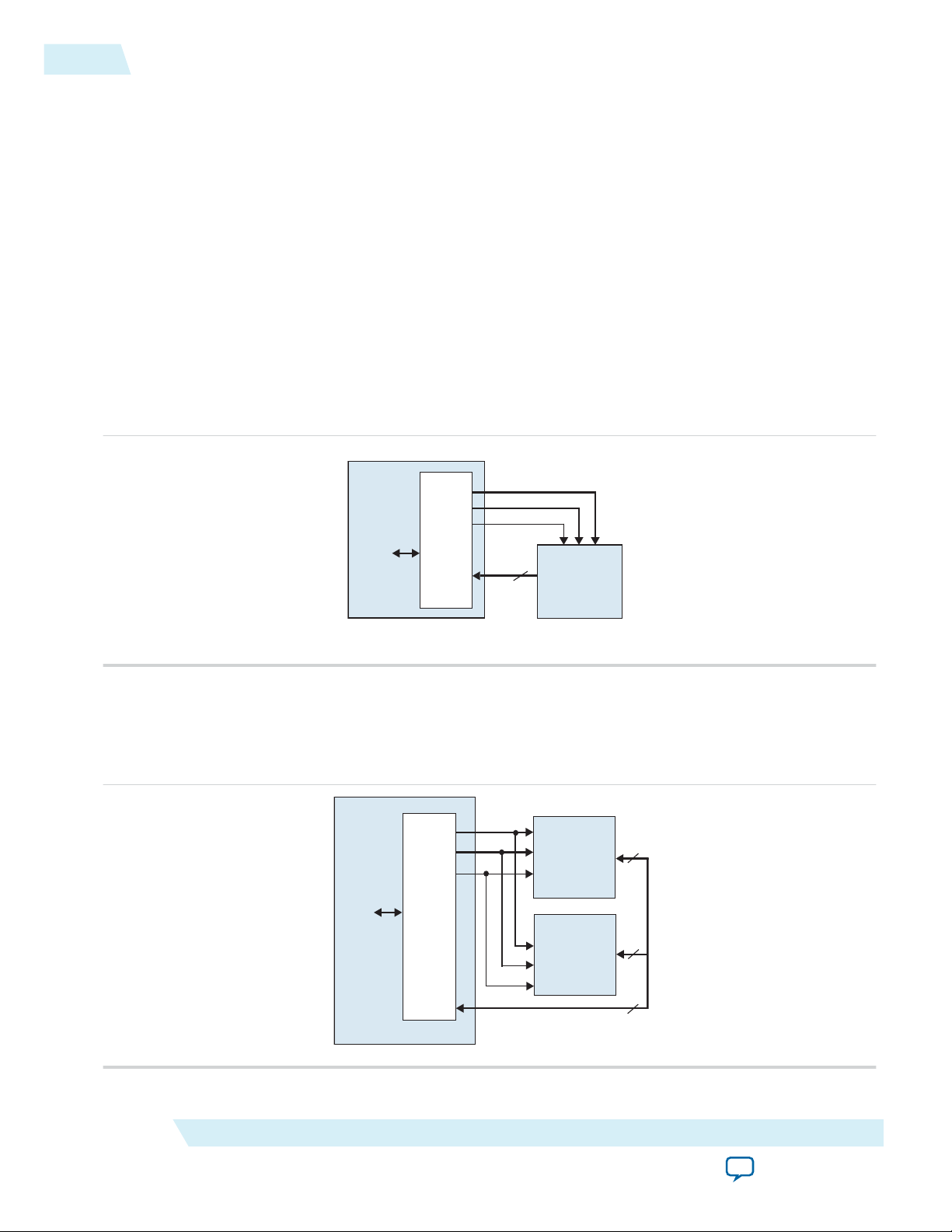
data
32
128 Mbits
16 Mbytes
32 data width device
SDRAM
Controller
Altera FPGA
Avalon-MM
interface
to
on-chip
logic
addr
cs_n
ctl
addr
ctl
cs_n
SDRAM
Controller
Altera FPGA
Avalon-MM
interface
to
on-chip
logic
64 Mbits
8 Mbytes
16 data width device
64 Mbits
8 Mbytes
16 data width device
data
16
16
32
2-8
Using the SDRAM Manufacturer's Memory Model
structured as a single, monolithic block of memory. For example, even for a system that combines two
SDRAM chips, the generic memory model is implemented as a single entity.
Using the SDRAM Manufacturer's Memory Model
If the Include a functional memory model the system testbench option is not enabled, you are
responsible for obtaining a memory model from the SDRAM manufacturer, and manually wiring the
model to the SDRAM controller pins in the system testbench.
Example Configurations
The following examples show how to connect the SDRAM controller outputs to an SDRAM chip or chips.
The bus labeled ctl is an aggregate of the remaining signals, such as cas_n, ras_n, cke and we_n.
The address, data, and control signals are wired directly from the controller to the chip. The result is a
128-Mbit (16-Mbyte) memory space.
Figure 2-2: Single 128-Mbit SDRAM Chip with 32-Bit Data
UG-01085
2014.24.07
Altera Corporation
The address and control signals connect in parallel to both chips. The chips share the chipselect (cs_n)
signal. Each chip provides half of the 32-bit data bus. The result is a logical 128-Mbit (16-Mbyte) 32-bit
data memory.
Figure 2-3: Two 64-MBit SDRAM Chips Each with 16-Bit Data
SDRAM Controller Core
Send Feedback
Page 25
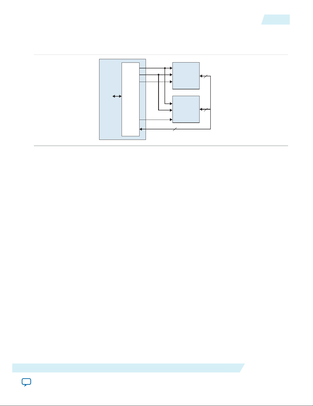
addr
ctl
cs_n [0]
cs_n [1]
SDRAM
Controller
Altera FPGA
Avalon-MM
interface
to
on-chip
logic
data
32
128 Mbits
16 Mbytes
32 data width device
128 Mbits
16 Mbytes
32 data width device
32
32
UG-01085
2014.24.07
The address, data, and control signals connect in parallel to the two chips. The chipselect bus (cs_n[1:0])
determines which chip is selected. The result is a logical 256-Mbit 32-bit wide memory.
Figure 2-4: Two 128-Mbit SDRAM Chips Each with 32-Bit Data
Software Programming Model
Software Programming Model
2-9
The SDRAM controller behaves like simple memory when accessed via the Avalon-MM interface. There
are no software-configurable settings and no memory-mapped registers. No software driver routines are
required for a processor to access the SDRAM controller.
Clock, PLL and Timing Considerations
This section describes issues related to synchronizing signals from the SDRAM controller core with the
clock that drives the SDRAM chip. During SDRAM transactions, the address, data, and control signals are
valid at the SDRAM pins for a window of time, during which the SDRAM clock must toggle to capture
the correct values. At slower clock frequencies, the clock naturally falls within the valid window. At higher
frequencies, you must compensate the SDRAM clock to align with the valid window.
Determine when the valid window occurs either by calculation or by analyzing the SDRAM pins with an
oscilloscope. Then use a PLL to adjust the phase of the SDRAM clock so that edges occur in the middle of
the valid window. Tuning the PLL might require trial-and-error effort to align the phase shift to the
properties of your target board.
For details about the PLL circuitry in your target device, refer to the appropriate device family handbook.
For details about configuring the PLLs in Altera devices, refer to the ALTPLL Megafunction User Guide.
Factors Affecting SDRAM Timing
The location and duration of the window depends on several factors:
SDRAM Controller Core
Send Feedback
Altera Corporation
Page 26

2-10
Symptoms of an Untuned PLL
• Timing parameters of the device and SDRAM I/O pins — I/O timing parameters vary based on device
family and speed grade.
• Pin location on the device — I/O pins connected to row routing have different timing than pins
connected to column routing.
• Logic options used during the Quartus II compilation — Logic options such as the Fast Input Register
and Fast Output Register logic affect the design fit. The location of logic and registers inside the
device affects the propagation delays of signals to the I/O pins.
• SDRAM CAS latency
As a result, the valid window timing is different for different combinations of FPGA and SDRAM
devices. The window depends on the Quartus II software fitting results and pin assignments.
Symptoms of an Untuned PLL
Detecting when the PLL is not tuned correctly might be difficult. Data transfers to or from the SDRAM
might not fail universally. For example, individual transfers to the SDRAM controller might succeed,
whereas burst transfers fail. For processor-based systems, if software can perform read or write data to
SDRAM, but cannot run when the code is located in SDRAM, the PLL is probably tuned incorrectly.
Estimating the Valid Signal Window
This section describes how to estimate the location and duration of the valid signal window using timing
parameters provided in the SDRAM datasheet and the Quartus II software compilation report. After
finding the window, tune the PLL so that SDRAM clock edges occur exactly in the middle of the window.
UG-01085
2014.24.07
Calculating the window is a two-step process. First, determine by how much time the SDRAM clock can
lag the controller clock, and then by how much time it can lead. After finding the maximum lag and lead
values, calculate the midpoint between them.
These calculations provide an estimation only. The following delays can also affect proper PLL tuning, but
are not accounted for by these calculations.
• Signal skew due to delays on the printed circuit board — These calculations assume zero skew.
• Delay from the PLL clock output nodes to destinations — These calculations assume that the delay
from the PLL SDRAM-clock output-node to the pin is the same as the delay from the PLL controllerclock output-node to the clock inputs in the SDRAM controller. If these clock delays are significantly
different, you must account for this phase shift in your window calculations.
Lag is a negative time shift, relative to the controller clock, and lead is a positive time shift. The
SDRAM clock can lag the controller clock by the lesser of the maximum lag for a read cycle or that for
a write cycle. In other words, Maximum Lag = minimum(Read Lag, Write Lag). Similarly, the SDRAM
clock can lead by the lesser of the maximum lead for a read cycle or for a write cycle. In other words,
Maximum Lead = minimum(Read Lead, Write Lead).
Altera Corporation
SDRAM Controller Core
Send Feedback
Page 27
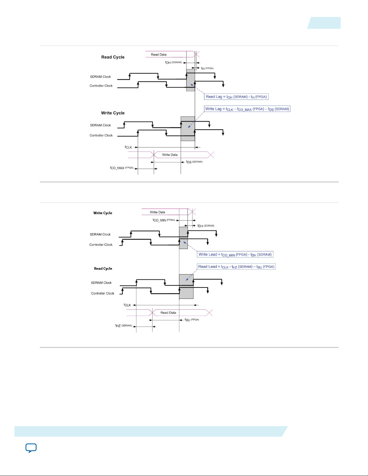
UG-01085
2014.24.07
Figure 2-5: Calculating the Maximum SDRAM Clock Lag
Figure 2-6: Calculating the Maximum SDRAM Clock Lead
Example Calculation
2-11
Example Calculation
This section demonstrates a calculation of the signal window for a Micron MT48LC4M32B2-7 SDRAM
chip and design targeting the Stratix II EP2S60F672C5 device. This example uses a CAS latency (CL) of 3
cycles, and a clock frequency of 50 MHz. All SDRAM signals on the device are registered in I/O cells,
enabled with the Fast Input Register and Fast Output Register logic options in the Quartus II software.
SDRAM Controller Core
Send Feedback
Altera Corporation
Page 28

2-12
Example Calculation
Table 2-3: Timing Parameters for Micron MT48LC4M32B2 SDRAM Device
UG-01085
2014.24.07
Parameter Symbol
Access time
from CLK
(pos. edge)
CL = 3 t
CL = 2 t
CL = 1 t
Address hold time t
Address setup time t
CLK high-level width t
CLK low-level width t
CL = 3 t
Clock cycle
time
CL = 2 t
CL = 1 t
CKE hold time t
CKE setup time t
CS#, RAS#, CAS#, WE#, DQM
hold time
AC(3)
AC(2)
AC(1)
AH
AS
CH
CL
CK(3)
CK(2)
CK(1)
CKH
CKS
t
CMH
Value (ns) in -7 Speed Grade
Min. Max.
— 5.5
— 8
— 17
1 —
2 —
2.75 —
2.75 —
7 —
10 —
20 —
1 —
2 —
1 —
CS#, RAS#, CAS#, WE#, DQM
t
CMS
setup time
Data-in hold time t
Data-in setup time t
Data-out
highimpedance
time
CL = 3 t
CL = 2 t
CL = 1 t
Data-out low-impedance time t
Data-out hold time t
DH
DS
HZ(3)
HZ(2)
HZ(1)
LZ
OH
The FPGA I/O Timing Parameters table below shows the relevant timing information, obtained from the
Timing Analyzer section of the Quartus II Compilation Report. The values in the table are the maximum
or minimum values among all device pins related to the SDRAM. The variance in timing between the
SDRAM pins on the device is small (less than 100 ps) because the registers for these signals are placed in
the I/O cell.
Table 2-4: FPGA I/O Timing Parameters
Parameter Symbol Value (ns)
Clock period t
Minimum clock-to-output time t
CLK
CO_MIN
2 —
1
2
5.5
— 8
— 17
1 —
2.5
20
2.399
Altera Corporation
SDRAM Controller Core
Send Feedback
Page 29

UG-01085
2014.24.07
Parameter Symbol Value (ns)
Document Revision History
2-13
Maximum clock-to-output time t
Maximum hold time after clock t
Maximum setup time before clock t
CO_MAX
H_MAX
SU_MAX
2.477
–5.607
5.936
You must compile the design in the Quartus II software to obtain the I/O timing information for the
design. Although Altera device family datasheets contain generic I/O timing information for each device,
the Quartus II Compilation Report provides the most precise timing information for your specific design.
The timing values found in the compilation report can change, depending on fitting, pin location, and
other Quartus II logic settings. When you recompile the design in the Quartus II software, verify that the
I/O timing has not changed significantly.
The following examples illustrate the calculations from figures Maximum SDRAM Clock Lag and
Maximum Lead also using the values from the Timing Parameters and FPGA I/O Timing Parameters
table.
The SDRAM clock can lag the controller clock by the lesser of Read Lag or Write Lag:
Read Lag = tOH(SDRAM) – t
H_MAX
(FPGA)
= 2.5 ns – (–5.607 ns) = 8.107 ns
or
Write Lag = t
CLK
– t
CO_MAX
(FPGA) – tDS(SDRAM)
= 20 ns – 2.477 ns – 2 ns = 15.523 ns
The SDRAM clock can lead the controller clock by the lesser of Read Lead or Write Lead:
Read Lead = t
CO_MIN
(FPGA) – tDH(SDRAM)
= 2.399 ns – 1.0 ns = 1.399 ns
or
Write Lead = t
CLK
– t
(SDRAM) – t
HZ(3)
= 20 ns – 5.5 ns – 5.936 ns = 8.564 ns
Therefore, for this example you can shift the phase of the SDRAM clock from –8.107 ns to 1.399 ns
relative to the controller clock. Choosing a phase shift in the middle of this window results in the value (–
8.107 + 1.399)/2 = –3.35 ns.
Document Revision History
Table 2-5: Document Revision History
Date and
Document
Version
July 2014
V14.0
-Removed mention of SOPC Builder, updated to Qsys Maintenance
SU_MAX
Changes Made Summary of Changes
(FPGA)
Release
SDRAM Controller Core
Send Feedback
Altera Corporation
Page 30

2-14
Document Revision History
UG-01085
2014.24.07
Date and
Document
Version
December
2010
v10.1.0
July 2010
v10.0.0
November
2009
v9.1.0
March 2009
v9.0.0
November
2008
v8.1.0
Changes Made Summary of Changes
Removed the “Device Support”, “Instantiating the Core in
—
SOPC Builder”, and “Referenced Documents” sections.
No change from previous release. —
No change from previous release. —
No change from previous release. —
Changed to 8-1/2 x 11 page size. No change to content. —
May 2008
No change from previous release. —
v8.0.0
For previous versions of this chapter, refer to the
Quartus II Handbook Archive.
Altera Corporation
SDRAM Controller Core
Send Feedback
Page 31

2014.24.07
www.altera.com
101 Innovation Drive, San Jose, CA 95134
Tri-State SDRAM
3
UG-01085
Subscribe
Send Feedback
The SDRAM controller core with Avalon® interface provides an Avalon Memory-Mapped (Avalon-MM)
interface to off-chip SDRAM. The SDRAM controller allows designers to create custom systems in an
Altera device that connect easily to SDRAM chips. The SDRAM controller supports standard SDRAM
defined by the PC100 specification.
SDRAM is commonly used in cost-sensitive applications requiring large amounts of volatile memory.
While SDRAM is relatively inexpensive, control logic is required to perform refresh operations, open-row
management, and other delays and command sequences. The SDRAM controller connects to one or more
SDRAM chips, and handles all SDRAM protocol requirements. The SDRAM controller core presents an
Avalon-MM slave port that appears as linear memory (flat address space) to Avalon-MM master
peripherals.
The Avalon-MM interface is latency-aware, allowing read transfers to be pipelined. The core can
optionally share its address and data buses with other off-chip Avalon-MM tri-state devices. This feature
is valuable in systems that have limited I/O pins, yet must connect to multiple memory chips in addition
to SDRAM.
The Tri-State SDRAM has the same functionality as the SDRAM Controller Core with the addition of the
Tri-State feature.
Avalon Interface Specifications
SDRAM Controller Core
Feature Description
The SDRAM controller core has the following features:
• Maximum frequency of 100-MHz
• Single clock domain design
• Sharing of dq/dqm/addr I/
©
2014 Altera Corporation. All rights reserved. ALTERA, ARRIA, CYCLONE, ENPIRION, MAX, MEGACORE, NIOS, QUARTUS and STRATIX words and logos are
trademarks of Altera Corporation and registered in the U.S. Patent and Trademark Office and in other countries. All other words and logos identified as
trademarks or service marks are the property of their respective holders as described at www.altera.com/common/legal.html. Altera warrants performance
of its semiconductor products to current specifications in accordance with Altera's standard warranty, but reserves the right to make changes to any
products and services at any time without notice. Altera assumes no responsibility or liability arising out of the application or use of any information,
product, or service described herein except as expressly agreed to in writing by Altera. Altera customers are advised to obtain the latest version of device
specifications before relying on any published information and before placing orders for products or services.
ISO
9001:2008
Registered
Page 32

altera _sdram_controller
Init FSM
Request
Buffer
Avalon-MM
Interface
SDRAM
Interface
Main
FSM
Signal Generation
Clock / Reset
Tri-state
Conduit
Master Signals
3-2
Block Diagram
Block Diagram
Figure 3-1: Tri-State SDRAM Block Diagram
UG-01085
2014.24.07
Configuration Parameter
The following table shows the configuration parameters available for user to program during generation
time of the IP core.
Memory Profile Page
The Memory Profile page allows you to specify the structure of the SDRAM subsystem such as address
and data bus widths, the number of chip select signals, and the number of banks.
Table 3-1: Configuration Parameters
Parameter GUI Legal Values Default Values Units
Data Width
Chip Selects
Architecture
Address Widths
Banks
Row
Column
8, 16, 32, 64 32 (Bit)s
1, 2, 4, 8 1 (Bit)s
2, 4 4 (Bit)s
11:14 12 (Bit)s
8:14 8 (Bit)s
Timing Page
Altera Corporation
The Timing page allows designers to enter the timing specifications of the Tri-State SDRAM chip(s) used.
The correct values are available in the manufacturer’s data sheet for the target SDRAM.
Tri-State SDRAM
Send Feedback
Page 33

UG-01085
2014.24.07
Table 3-2: Configuration Timing Parameters
Parameter GUI Legal Values Default Values Units
CAS latency cycles 1, 2, 3 3 Cycles
Initialization refresh cycles 1:8 2 Cycles
Interface
3-3
Issue one refresh command
0.0:156.25 15.625 us
every
Delay after power up, before
0.0:999.0 100.00 us
initialization
Duration of refresh command
0.0:700.0 70.0 ns
(t_rfc)
Duration of precharge
0.0:200.0 20.0 ns
command (t_rp)
ACTIVE to READ or WRITE
0.0:200.0 20.0 ns
delay (t_rcd)
Access time (t_ac) 0.0:999.0 5.5 ns
Write recovery time (t_wr, no
0.0:140.0 14.0 ns
auto precharge)
Interface
The following are top level signals from the SDRAM controller Core
Table 3-3: Clock and Reset Signals
Signal Width Direction Description
clk
rst_n
Tri-State SDRAM
1 Input System Clock
1 Input System asynchronous reset.
The signal is asserted
asynchronously, but is deasserted synchronously after
the rising edge of ssi_clk.
The synchronization must be
provided external to this
component.
Altera Corporation
Send Feedback
Page 34

3-4
Interface
Table 3-4: Avalon-MM Slave Interface Signals
Signal Width Direction Description
UG-01085
2014.24.07
avs_read
avs_write
avs_byteenable dqm_width
avs_address controller_addr_
avs_writedata sdram_data_width
avs_readdata sdram_data_width
1 Input Avalon-MM read control.
1 Input Avalon-MM write control.
width
Asserted to indicate a read
transfer. If present, readdata
is required.
Asserted to indicate a write
transfer. If present,
writedata is required.
Input Enables specific byte lane(s)
during transfer. Each bit
corresponds to a byte in avs_
writedata and avs_
readdata.
Input Avalon-MM address bus.
Input Avalon-MM write data bus.
Driven by the bus master
(bridge unit) during write
cycles.
Output Avalon-MM readback data.
Driven by the altera_spi
during read cycles.
avs_readdatavalid
avs_waitrequest
Altera Corporation
1 Output Asserted to indicate that the
avs_readdata signals
contains valid data in
response to a previous read
request.
1 Output Asserted when it is unable to
respond to a read or write
request.
Tri-State SDRAM
Send Feedback
Page 35

UG-01085
2014.24.07
Table 3-5: Tristate Conduit Master / SDRAM Interface Signals
Signal Width Direction Description
Interface
3-5
tcm_grant
1 Input When asserted, indicates that
a tristate conduit master has
been granted access to
perform transactions. tcm_
grant is asserted in
response to the tcm_request
signal and remains asserted
until 1 cycle following the
deassertion of request.
Valid only when pin sharing
mode is enabled.
Tri-State SDRAM
Send Feedback
Altera Corporation
Page 36

3-6
Interface
Signal Width Direction Description
UG-01085
2014.24.07
tcm_request
1 Output The meaning of tcm_
request depends on the
state of the tcm_grant
signal, as the following rules
dictate:
• When tcm_request is
asserted and tcm_grant is
deasserted, tcm_request
is requesting access for
the current cycle.
• When tcm_request is
asserted and tcm_grant is
asserted, tcm_request is
requesting access for the
next cycle; consequently,
tcm_request should be
deasserted on the final
cycle of an access.
Because tcm_request is
deasserted in the last cycle of
a bus access, it can be
reasserted immediately
following the final cycle of a
transfer, making both
rearbitration and continuous
bus access possible if no
other masters are requesting
access.
sdram_dq_width
sdram_dq_in sdram_data_width
Altera Corporation
sdram_data_width
Once asserted, tcm_request
must remain asserted until
granted; consequently, the
shortest bus access is 2
cycles.
Valid only when pin-sharing
mode is enabled.
Output SDRAM data bus output.
Valid only when pin-sharing
mode is enabled
Input SDRAM data bus output.
Valid only when pin-sharing
mode is enabled.
Tri-State SDRAM
Send Feedback
Page 37

UG-01085
2014.24.07
Interface
Signal Width Direction Description
3-7
sdram_dq_oen
sdram_dq sdram_data_width
sdram_addr sdram_addr_width
sdram_ba sdram_bank_width
sdram_dqm dqm_width
sdram_ras_n
1 Output SDRAM data bus input.
1 Output Row Address Select. When
Valid only when pin-sharing
mode is enabled.
Input/Output SDRAM data bus.
Valid only when pin-sharing
mode is disabled.
Output SDRAM address bus.
Output SDRAM bank address.
Output SDRAM data mask. When
asserted, it indicates to the
SDRAM chip that the
corresponding data signal is
suppressed. There is one
DQM line per 8 bits data
lines
taken LOW, the value on the
tcm_addr_out bus is used to
select the bank and activate
the required row.
sdram_cas_n
sdram_we_n
sdram_cs_n
1 Output Column Address Select.
When taken LOW, the value
on the tcm_addr_out bus is
used to select the bank and
required column. A read or
write operation will then be
conducted from that
memory location, depending
on the state of tcm_we_out.
1 Output SDRAM Write Enable,
determins whether the
location addressed by tcm_
addr_out is written to or
read from.
0=Read
1=Write
Output SDRAM Chip Select. When
taken LOW, will enables the
SDRAM device.
Tri-State SDRAM
Send Feedback
Altera Corporation
Page 38

3-8
Reset and Clock Requirements
Signal Width Direction Description
UG-01085
2014.24.07
sdram_cke
1 Output SDRAM Clock Enable. The
Note: The SDRAM controller does not have any configurable control status registers (CSR).
Reset and Clock Requirements
The main reset input signal to the SDRAM is treated as an asynchronous reset input from the SDRAM
core perspective. A reset synchronizer circuit, as typically implemented for each reset domain in a
complete SOC/ASIC system is not implemented within the SDRAM core. Instead, this reset synchronizer
circuit should be implemented externally to the SDRAM, in a higher hierarchy within the complete
system design, so that the “asynchronous assertion, synchronous de-assertion” rule is fulfilled.
The SDRAM core accepts an input clock at its clk input with maximum frequency of 100-MHz. The
other requirements for the clock, such as its minimum frequency should be similar to the requirement of
the external SDRAM which the SDRAM is interfaced to.
SDRAM controller does not
support clock-disable modes.
The SDRAM controller
permanently asserts the tcm_
sdr_cke_out signal on the
SDRAM.
Architecture
The SDRAM Controller connects to one or more SDRAM chips, and handles all SDRAM protocol
requirements. Internal to the device, the core presents an Avalon-MM slave ports that appears as a linear
memory (flat address space) to Avalon-MM master device.
The core can access SDRAM subsystems with:
• Various data widths (8-, 16-, 32- or 64-bits)
• Various memory sizes
• Multiple chip selects
The Avalon-MM interface is latency-aware, allowing read transfers to be pipelined. The core can
optionally share its address and data buses with other off-chip Avalon-MM tri-state devices.
Limitations: for now the arbitration control of this mode should be handled by the host/master in
Note:
the system to avoid a device monopolizing the shared buses.
Control logic within the SDRAM core responsible for the main functionality listed below, among others:
• Refresh operation
• Open_row management
• Delay and command management
Use of the data bus is intricate and thus requires a complex DRAM controller circuit. This is because data
written to the DRAM must be presented in the same cycle as the write command, but reads produce
output 2 or 3 cycles after the read command. The SDRAM controller must ensure that the data bus is
never required for a read and a write at the same time.
Altera Corporation
Tri-State SDRAM
Send Feedback
Page 39

UG-01085
2014.24.07
Avalon-MM Slave Interface and CSR
The host processor perform data read and write operation to the external SDRAM devices through the
Avalon-MM interface of the SDRAM core.
Avalon Interface SpecificationsPlease refer to Avalon Interface Specifications for more information on
the details of the Avalon-MM Slave Interface.
Block Level Usage Model
Figure 3-2: Shared-Bus System
Avalon-MM Slave Interface and CSR
3-9
Tri-State SDRAM
Send Feedback
Altera Corporation
Page 40

3-10
Document Revision History
Document Revision History
Table 3-6: Document Revision History
UG-01085
2014.24.07
Date and
Document
Version
July 2014
v14.0
Changes Made Summary of Changes
- Initial Release
Altera Corporation
Tri-State SDRAM
Send Feedback
Page 41

2014.24.07
Avalon-to-
CompactFlash
Avalon-MM
Master
(e.g. CPU)
System Interconnect Fabric
Altera FPGA
CompactFlash
Device
e
d
i
a
l
S
M
M
n
o
l
a
v
A
r
o
P
e
v
t
ctl
a
l
S
M
M
n
o
l
a
v
A
r
o
P
e
v
t
data
address
cfctl
idectl
Registers
IRQ
data
address
IRQ
www.altera.com
101 Innovation Drive, San Jose, CA 95134
Compact Flash Core
4
UG-01085
Subscribe
Send Feedback
Core Overview
The CompactFlash core allows you to connect systems built on Osys to CompactFlash storage cards in
true IDE mode by providing an Avalon® Memory-Mapped (Avalon-MM) interface to the registers on the
storage cards. The core supports PIO mode 0.
The CompactFlash core also provides an Avalon-MM slave interface which can be used by Avalon-MM
master peripherals such as a Nios® II processor to communicate with the CompactFlash core and manage
its operations.
Functional Description
Figure 4-1: System With a CompactFlash Core
As shown in the block diagram, the CompactFlash core provides two Avalon-MM slave interfaces: the ide
slave port for accessing the registers on the CompactFlash device and the ctl slave port for accessing the
core's internal registers. These registers can be used by Avalon-MM master peripherals such as a Nios II
processor to control the operations of the CompactFlash core and to transfer data to and from the
CompactFlash device.
You can set the CompactFlash core to generate two active-high interrupt requests (IRQs): one signals the
insertion and removal of a CompactFlash device and the other passes interrupt signals from the Compact‐
Flash device.
©
2014 Altera Corporation. All rights reserved. ALTERA, ARRIA, CYCLONE, ENPIRION, MAX, MEGACORE, NIOS, QUARTUS and STRATIX words and logos are
trademarks of Altera Corporation and registered in the U.S. Patent and Trademark Office and in other countries. All other words and logos identified as
trademarks or service marks are the property of their respective holders as described at www.altera.com/common/legal.html. Altera warrants performance
of its semiconductor products to current specifications in accordance with Altera's standard warranty, but reserves the right to make changes to any
products and services at any time without notice. Altera assumes no responsibility or liability arising out of the application or use of any information,
product, or service described herein except as expressly agreed to in writing by Altera. Altera customers are advised to obtain the latest version of device
specifications before relying on any published information and before placing orders for products or services.
ISO
9001:2008
Registered
Page 42

4-2
Required Connections
The CompactFlash core maps the Avalon-MM bus signals to the CompactFlash device with proper
timing, thus allowing Avalon-MM master peripherals to directly access the registers on the CompactFlash
device.
Compact Flash
For more information, refer to the CF+ and CompactFlash specifications available at www.compactflash.org.
Required Connections
The table below lists the required connections between the CompactFlash core and the CompactFlash
device.
Table 4-1: Core to Device Required Connections
UG-01085
2014.24.07
CompactFlash Interface Signal
Name
addr[0] Output 20
addr[1] Output 19
addr[2] Output 18
addr[3] Output 17
addr[4] Output 16
addr[5] Output 15
addr[6] Output 14
addr[7] Output 12
addr[8] Output 11
addr[9] Output 10
addr[10] Output 8
atasel_n Output 9
cs_n[0] Output 7
cs_n[1] Output 32
Pin Type CompactFlash Pin
Number
Altera Corporation
data[0] Input/Output 21
data[1] Input/Output 22
data[2] Input/Output 23
data[3] Input/Output 2
data[4] Input/Output 3
data[5] Input/Output 4
data[6] Input/Output 5
Compact Flash Core
Send Feedback
Page 43

UG-01085
2014.24.07
Software Programming Model
4-3
CompactFlash Interface Signal
Name
data[7] Input/Output 6
data[8] Input/Output 47
data[9] Input/Output 48
data[10] Input/Output 49
data[11] Input/Output 27
data[12] Input/Output 28
data[13] Input/Output 29
data[14] Input/Output 30
data[15] Input/Output 31
detect Input 25 or 26
intrq Input 37
iord_n Output 34
iordy Input 42
iowr_n Output 35
Pin Type CompactFlash Pin
Number
power Output CompactFlash power
reset_n Output 41
rfu Output 44
we_n Output 46
Software Programming Model
This section describes the software programming model for the CompactFlash core.
HAL System Library Support
The Altera-provided HAL API functions include a device driver that you can use to initialize the
CompactFlash core. To perform other operations, use the low-level macros provided.
Software Files
For more information on the macros, refer to the Software Files section.
Software Files
The CompactFlash core provides the following software files. These files define the low-level access to the
hardware. Application developers should not modify these files.
controller, if present
Compact Flash Core
Send Feedback
Altera Corporation
Page 44

4-4
Register Maps
• altera_avalon_cf_regs.h—The header file that defines the core's register maps.
• altera_avalon_cf.h, altera_avalon_cf.c—The header and source code for the functions and variables
required to integrate the driver into the HAL system library.
Register Maps
This section describes the register maps for the Avalon-MM slave interfaces.
Ide Registers
The ide port in the CompactFlash core allows you to access the IDE registers on a CompactFlash device.
Table 4-2: Ide Register Map
UG-01085
2014.24.07
Offset
Read Operation Write Operation
Register Names
0 RD Data WR Data
1 Error Features
2 Sector Count Sector Count
3 Sector No Sector No
4 Cylinder Low Cylinder Low
5 Cylinder High Cylinder High
6 Select Card/Head Select Card/Head
7 Status Command
14 Alt Status Device Control
Ctl Registers
The ctl port in the CompactFlash core provides access to the registers which control the core’s operation
and interface.
Table 4-3: Ctl Register Map
Offset Register
0 cfctl Reserved IDET RST PWR DET
1 idectl Reserved IIDE
2 Reserved Reserved
3 Reserved Reserved
Cfctl Register
The cfctl register controls the operations of the CompactFlash core. Reading the cfctl register clears the
interrupt.
Altera Corporation
Fields
31:4 3 2 1 0
Compact Flash Core
Send Feedback
Page 45

UG-01085
2014.24.07
Table 4-4: cfctl Register Bits
Bit Number Bit Name Read/Write Description
0 DET RO Detect. This bit is set to 1 when the core detects a
1 PWR RW Power. When this bit is set to 1, power is being supplied to
2 RST RW Reset. When this bit is set to 1, the CompactFlash device is
3 IDET RW Detect Interrupt Enable. When this bit is set to 1, the
idectl Register
The idectl register controls the interface to the CompactFlash device.
Table 4-5: idectl Register
idectl Register
CompactFlash device.
the CompactFlash device.
held in a reset state. Setting this bit to 0 returns the device
to its active state.
CompactFlash core generates an interrupt each time the
value of the det bit changes.
4-5
Bit Number Bit Name Read/Write Description
0 IIDE RW IDE Interrupt Enable. When this bit is set to 1, the
CompactFlash core generates an interrupt following an
interrupt generated by the CompactFlash device. Setting
this bit to 0 disables the IDE interrupt.
Document Revision History
Table 4-6: Document Revision History
Date and
Document
Version
July 2014
v14.0
December
2010
v10.1.0
-Removed metion of SOPC Builder, updated to Qsys Maintance Release
Removed the “Device Support”, “Instantiating the Core in
SOPC Builder”, and “Referenced Documents” sections.
Changes Made Summary of Changes
—
July 2010
v10.0.0
Compact Flash Core
Send Feedback
No change from previous release. —
Altera Corporation
Page 46

4-6
Document Revision History
UG-01085
2014.24.07
Date and
Document
Version
November
No change from previous release. —
Changes Made Summary of Changes
2009
v9.1.0
March 2009
No change from previous release. —
v9.0.0
November
Changed to 8-1/2 x 11 page size. No change to content. —
2008
v8.1.0
May 2008
Added the mode supported by the CompactFlash core. —
v8.0.0
For previous versions of this chapter, refer to the Quartus II Handbook Archive.
Altera Corporation
Compact Flash Core
Send Feedback
Page 47

2014.24.07
www.altera.com
101 Innovation Drive, San Jose, CA 95134
Common Flash Interface Controller Core
5
UG-01085
Core Overview
The common flash interface controller core with Avalon® interface (CFI controller) allows you to easily
connect Qsys systems to external flash memory that complies with the Common Flash Interface (CFI)
specification. The CFI controller is Qsys-ready and integrates easily into any Qsys-generated system.
For the Nios® II processor, Altera provides hardware abstraction layer (HAL) driver routines for the CFI
controller. The drivers provide universal access routines for CFI-compliant flash memories. Therefore,
you do not need to write any additional code to program CFI-compliant flash devices. The HAL driver
routines take advantage of the HAL generic device model for flash memory, which allows you to access
the flash memory using the familiar HAL application programming interface (API), the ANSI C standard
library functions for file I/O, or both.
The Nios II Embedded Design Suite (EDS) provides a flash programmer utility based on the Nios II
processor and the CFI controller. The flash programmer utility can be used to program any CFIcompliant flash memory connected to an Altera® device.
Nios II Software Developer's Handbook
Subscribe
Send Feedback
For more information about how to read and write flash using the HAL API, refer to the .
Nios II Flash Programmer User Guide
For more information on the flash programmer utility, refer to the .
www.intel.com
Further information about the Common Flash Interface specification is available at .
www.amd.com
As an example of a flash device supported by the CFI controller, see the data sheet for the AMD
Am29LV065D-120R, available at .
The common flash interface controller core supersedes previous Altera flash cores distributed with Qsys
or Nios development kits. All flash chips associated with these previous cores comply with the CFI specifi‐
cation, and therefore are supported by the CFI controller.
©
2014 Altera Corporation. All rights reserved. ALTERA, ARRIA, CYCLONE, ENPIRION, MAX, MEGACORE, NIOS, QUARTUS and STRATIX words and logos are
trademarks of Altera Corporation and registered in the U.S. Patent and Trademark Office and in other countries. All other words and logos identified as
trademarks or service marks are the property of their respective holders as described at www.altera.com/common/legal.html. Altera warrants performance
of its semiconductor products to current specifications in accordance with Altera's standard warranty, but reserves the right to make changes to any
products and services at any time without notice. Altera assumes no responsibility or liability arising out of the application or use of any information,
product, or service described herein except as expressly agreed to in writing by Altera. Altera customers are advised to obtain the latest version of device
specifications before relying on any published information and before placing orders for products or services.
ISO
9001:2008
Registered
Page 48

System Interconnect Fabric
S
Avalon-MM Slave Port
M Avalon-MM Master Port
Avalon-MM Tristate Bridge
S
S
M
M
Avalon-MM
Master
(e.g. CPU)
S
On-Chip
Slave
Peripheral
Altera FPGA
S
Flash
Memory
Chip
S
Other
Memory
chipselect,
read_n, write_n
chipselect,
read_n, write_n
flash
other
5-2
Functional Description
Functional Description
The figure below shows a block diagram of the CFI controller in a typical system configuration. The
Avalon Memory-Mapped (Avalon-MM) interface for flash devices is connected through an Avalon-MM
tristate bridge. The tristate bridge creates an off-chip memory bus that allows the flash chip to share
address and data pins with other memory chips. It provides separate chipselect, read, and write pins to
each chip connected to the memory bus. The CFI controller hardware is minimal; it is simply an AvalonMM tristate slave port configured with waitstates, setup, and hold time appropriate for the target flash
chip. This slave port is capable of Avalon-MM tristate slave read and write transfers.
Figure 5-1: System Integrating a CFI Controller
UG-01085
2014.24.07
Configuration
Attributes Page
Preset Settings
Altera Corporation
Avalon-MM master ports can perform read transfers directly from the CFI controller's Avalon-MM port.
See the Software Programming Model section for more detail on writing/erasing flash memory.
The following sections describe the available configuration options.
The options on this page control the basic hardware configuration of the CFI controller.
The Presets setting is a drop-down menu of flash chips that have already been characterized for use with
the CFI controller. After you select one of the chips in the Presets menu, the wizard updates all settings on
both tabs (except for the Board Info setting) to work with the specified flash chip.
Common Flash Interface Controller Core
Send Feedback
Page 49

UG-01085
2014.24.07
Setting Size
Timing page
Setting Size
5-3
The options provided are not intended to cover the wide range of flash devices available in the market. If
the flash chip on your target board does not appear in the Presets list, you must configure the other
settings manually.
The size setting specifies the size of the flash device. There are two settings:
• Address Width—The width of the flash chip's address bus.
• Data Width—The width of the flash chip's data bus
The size settings cause Qsys to allocate the correct amount of address space for this device. Qsys will
automatically generate dynamic bus sizing logic that appropriately connects the flash chip to Avalon-MM
master ports of different data widths.
Avalon Interface Specifications
For details about dynamic bus sizing, refer to the Avalon Interface Specifications.
The options on this page specify the timing requirements for read and write transfers with the flash
device.
Refer to the specifications provided with the common flash device you are using to obtain the timing
values you need to calculate the values of the parameters on the Timing page.
The settings available on the Timing page are:
• Setup—After asserting chipselect, the time required before asserting the read or write signals. You can
determine the value of this parameter by using the following formula:
Setup = tCE (chip enable to output delay) - tOE (output enable to output delay)
• Wait—The time required for the read or write signal to be asserted for each transfer. Use the following
guideline to determine an appropriate value for this parameter:
The sum of Setup, Wait, and board delay must be greater than tACC, where:
• Board delay is determined by the TCO on the FPGA address pins, TSU on the device data pins, and
propagation delay on the board traces in both directions.
• tACC is the address to output delay.
• Hold—After deasserting the write signal, the time required before deasserting the chipselect signal.
• Units—The timing units used for the Setup, Wait, and Hold values. Possible values include ns, μs, ms,
and clock cycles.
Avalon Interface Specifications
For more information about signal timing for the Avalon-MM interface, refer to the Avalon Interface
Specifications.
Software Programming Model
This section describes the software programming model for the CFI controller. In general, any AvalonMM master in the system can read the flash chip directly as a memory device. For Nios II processor users,
Altera provides HAL system library drivers that enable you to erase and write the flash memory using the
HAL API functions.
Common Flash Interface Controller Core
Send Feedback
Altera Corporation
Page 50

5-4
HAL System Library Support
HAL System Library Support
The Altera-provided driver implements a HAL flash device driver that integrates into the HAL system
library for Nios II systems. Programs call the familiar HAL API functions to program CFI-compliant flash
memory. You do not need to know anything about the details of the underlying drivers.
Nios II Software Developer's Handbook.
The HAL API for programming flash, including C code examples, is described in detail in the Nios II
Software Developer's Handbook.
The Nios II EDS also provides a reference design called Flash Tests that demonstrates erasing, writing,
and reading flash memory.
Limitations
Currently, the Altera-provided drivers for the CFI controller support only Intel, AMD and Spansion flash
chips.
Software Files
The CFI controller provides the following software files. These files define the low-level access to the
hardware, and provide the routines for the HAL flash device driver. Application developers should not
modify these files.
UG-01085
2014.24.07
• altera_avalon_cfi_flash.h, altera_avalon_cfi_flash.c—The header and source code for the functions and
variables required to integrate the driver into the HAL system library.
• altera_avalon_cfi_flash_funcs.h, altera_avalon_cfi_flash_table.c—The header and source code for functions
concerned with accessing the CFI table.
• altera_avalon_cfi_flash_amd_funcs.h, altera_avalon_cfi_flash_amd.c—The header and source code for
programming AMD CFI-compliant flash chips.
• altera_avalon_cfi_flash_intel_funcs.h, altera_avalon_cfi_flash_intel.c—The header and source code for
programming Intel CFI-compliant flash chips.
Document Revision History
Table 5-1: Document Revision History
Date and
Document
Version
July 2014
v14.0.0
December
2010
v10.1.0
-Removed mention of SOPC Builder, updated to Qsys Maintenance Release
Removed the “Device Support”, “Instantiating the Core
in SOPC Builder”, and “Referenced Documents”
sections.
Changes Made Summary of Changes
—
July 2010
v10.0.0
Altera Corporation
No change from previous release. —
Common Flash Interface Controller Core
Send Feedback
Page 51

UG-01085
2014.24.07
Document Revision History
5-5
Date and
Document
Version
November
Revised description of the timing page settings. —
Changes Made Summary of Changes
2009
v9.1.0
March 2009
No change from previous release. —
v9.0.0
November
2008
Changed to 8-1/2 x 11 page size. Added description to
parameters on Timing page.
—
v8.1.0
May 2008
v8.0.0
Updated the CFI controllers supported by Alteraprovided drivers.
Updates made to
comply with the
Quartus II software
version 8.0 release.
For previous versions of this chapter, refer to the Quartus II Handbook Archive.
Common Flash Interface Controller Core
Send Feedback
Altera Corporation
Page 52

2014.24.07
www.altera.com
101 Innovation Drive, San Jose, CA 95134
EPCS Serial Flash Controller Core
6
UG-01085
Core Overview
The EPCS serial flash controller core with Avalon® interface allows Nios® II systems to access an Altera
EPCS serial configuration device. Altera provides drivers that integrate into the Nios II hardware
abstraction layer (HAL) system library, allowing you to read and write the EPCS device using the familiar
HAL application program interface (API) for flash devices.
Using the EPCS serial flash controller core, Nios II systems can:
• Store program code in the EPCS device. The EPCS serial flash controller core provides a boot-loader
feature that allows Nios II systems to store the main program code in an EPCS device.
• Store non-volatile program data, such as a serial number, a NIC number, and other persistent data.
• Manage the device configuration data. For example, a network-enabled embedded system can receive
new FPGA configuration data over a network, and use the core to program the new data into an EPCS
serial configuration device.
The EPCS serial flash controller core is Qsys-ready and integrates easily into any Qsys-generated
system. The flash programmer utility in the Nios II IDE allows you to manage and program data
contents into the EPCS device.
Serial Configuration Devices (EPCS1, EPCS4, EPCS16, EPCS64 and EPCS128) Data Sheet
For information about the EPCS serial configuration device family, refer to the Serial Configuration
Devices Data Sheet.
Subscribe
Send Feedback
®
Nios II Software Developer's Handbook
For details about using the Nios II HAL API to read and write flash memory, refer to the Nios II
Software Developer's Handbook.
Nios II Flash Programmer User Guide
For details about managing and programming the EPCS memory contents, refer to the Nios II Flash
Programmer User Guide.
For Nios II processor users, the EPCS serial flash controller core supersedes the Active Serial Memory
Interface (ASMI) device. New designs should use the EPCS serial flash controller core instead of the
ASMI core.
©
2014 Altera Corporation. All rights reserved. ALTERA, ARRIA, CYCLONE, ENPIRION, MAX, MEGACORE, NIOS, QUARTUS and STRATIX words and logos are
trademarks of Altera Corporation and registered in the U.S. Patent and Trademark Office and in other countries. All other words and logos identified as
trademarks or service marks are the property of their respective holders as described at www.altera.com/common/legal.html. Altera warrants performance
of its semiconductor products to current specifications in accordance with Altera's standard warranty, but reserves the right to make changes to any
products and services at any time without notice. Altera assumes no responsibility or liability arising out of the application or use of any information,
product, or service described herein except as expressly agreed to in writing by Altera. Altera customers are advised to obtain the latest version of device
specifications before relying on any published information and before placing orders for products or services.
ISO
9001:2008
Registered
Page 53

System Interconnect Fabric
EPCS
Controller Core
Boot-Loader
ROM
EPCS Serial
Configuration
Device
Config
Memory
General-
Purpose
Memory
Nios II CPU
Other
On-Chip
Peripheral(s)
Altera FPGA
6-2
Functional Description
Functional Description
As shown below, the EPCS device's memory can be thought of as two separate regions:
• FPGA configuration memory—FPGA configuration data is stored in this region.
• General-purpose memory—If the FPGA configuration data does not fill up the entire EPCS device,
any left-over space can be used for general-purpose data and system startup code.
Figure 6-1: Nios II System Integrating an EPCS Serial Flash Controller Core
UG-01085
2014.24.07
• By virtue of the HAL generic device model for flash devices, accessing the EPCS device using the HAL
The EPCS serial flash controller core contains an on-chip memory for storing a boot-loader program.
When used in conjunction with Cyclone® and Cyclone II devices, the core requires 512 bytes of bootloader ROM. For Cyclone III, Cyclone IV, Stratix® II, and newer device families in the Stratix series, the
core requires 1 KByte of boot-loader ROM. The Nios II processor can be configured to boot from the
EPCS serial flash controller core. To do so, set the Nios II reset address to the base address of the EPCS
serial flash controller core. In this case, after reset the CPU first executes code from the boot-loader ROM,
which copies data from the EPCS general-purpose memory region into a RAM. Then, program control
transfers to the RAM. The Nios II IDE provides facilities to compile a program for storage in the EPCS
device, and create a programming file to program into the EPCS device.
Nios II Flash Programmer User Guide
For more information, refer to the Nios II Flash Programmer User Guide..
If you program the EPCS device using the Quartus® II Programmer, all previous content is erased. To
program the EPCS device with a combination of FPGA configuration data and Nios II program data, use
the Nios II IDE flash programmer utility.
The Altera EPCS configuration device connects to the FPGA through dedicated pins on the FPGA, not
through general-purpose I/O pins. In all Altera device families except Cyclone III and Cyclone IV, the
EPCS serial flash controller core does not create any I/O ports on the top-level Qsys system module. If the
EPCS device and the FPGA are wired together on a board for configuration using the EPCS device (in
Altera Corporation
other words, active serial configuration mode), no further connection is necessary between the EPCS
serial flash controller core and the EPCS device. When you compile the Qsys system in the Quartus II
API is the same as accessing any flash memory. The EPCS device has a special-purpose hardware
interface, so Nios II programs must read and write the EPCS memory using the provided HAL flash
drivers.
EPCS Serial Flash Controller Core
Send Feedback
Page 54

UG-01085
2014.24.07
Avalon-MM Slave Interface and Registers
6-3
software, the EPCS serial flash controller core signals are routed automatically to the device pins for the
EPCS device.
You, however, have the option not to use the dedicated pins on the FPGA (active serial configuration
mode) by turning off the respective parameters in the MegaWizard interface. When this option is turned
off or when the target device is a Cyclone III or Cyclone IV device, you have the flexibility to connect the
output pins, which are exported to the top-level design, to any EPCS devices. Perform the following tasks
in the Quartus® II software to make the necessary pin assignments:
• On the Dual-purpose pins page (Assignments > Devices > Device and Pin Options), ensure that the
following pins are assigned to the respective values:
• Data[0] = Use as regular I/O
• Data[1] = Use as regularr I/O
• DCLK = Use as regular I/O
• FLASH_nCE/nCS0 = Use as regular I/O
• Using the Pin Planner (Assignments > Pins), ensure that the following pins are assigned to the
respective configuration functions on the device:
• data0_to_the_epcs_controller = DATA0
• sdo_from the_epcs_controller = DATA1,ASDO
• dclk_from_epcs_controller = DCLK
• sce_from_the_epcs_controller = FLASH_nCE
Pin-Out Files for Altera Device
For more information about the configuration pins in Altera devices, refer to the Pin-Out Files for Altera
Device page.
Avalon-MM Slave Interface and Registers
The EPCS serial flash controller core has a single Avalon-MM slave interface that provides access to both
boot-loader code and registers that control the core. As shown in below, the first segment is dedicated to
the boot-loader code, and the next seven words are control and data registers. A Nios II CPU can read the
instruction words, starting from the core's base address as flat memory space, which enables the CPU to
reset the core's address space.
The EPCS serial flash controller core includes an interrupt signal that can be used to interrupt the CPU
when a transfer has completed.
Table 6-1: EPCS Serial Flash Controller Core Register Map
Offset
(32-bit Word Address)
0x00 .. 0xFF Boot ROM Memory R Boot Loader
Register Name R/W
Bit Description
Code
31:0
EPCS Serial Flash Controller Core
Send Feedback
Altera Corporation
Page 55

6-4
Configuration
UG-01085
2014.24.07
Offset
(32-bit Word Address)
0x100 Read Data R
0x101 Write Data W
0x102 Status R/W
0x103 Control R/W
0x104 Reserved —
0x105 Slave Enable R/W
0x106 End of Packet R/W
Register Name R/W
Note: Altera does not publish the usage of the control and data registers. To access the EPCS device, you
must use the HAL drivers provided by Altera.
Configuration
The core must be connected to a Nios II processor. The core provides drivers for HAL-based Nios II
systems, and the precompiled boot loader code compatible with the Nios II processor.
In device families other than Cyclone III and Cyclone IV, you can use the MegaWizard™ interface to
configure the core to use general I/O pins instead of dedicated pins by turning off both parameters,
Automatically select dedicated active serial interface, if supported and Use dedicated active serial
interface.
Bit Description
31:0
Only one EPCS serial flash controller core can be instantiated in each FPGA design.
Software Programming Model
This section describes the software programming model for the EPCS serial flash controller core. Altera
provides HAL system library drivers that enable you to erase and write the EPCS memory using the HAL
API functions. Altera does not publish the usage of the cores registers. Therefore, you must use the HAL
drivers provided by Altera to access the EPCS device.
HAL System Library Support
The Altera-provided driver implements a HAL flash device driver that integrates into the HAL system
library for Nios II systems. Programs call the familiar HAL API functions to program the EPCS memory.
You do not need to know the details of the underlying drivers to use them.
The driver for the EPCS device is excluded when the reduced device drivers option is enabled in a BSP or
system library. To force inclusion of the EPCS drivers in a BSP with the reduced device drivers option
enabled, you can define the preprocessor symbol, ALT_USE_EPCS_FLASH, before including the header, as
follows:
#define ALT_USE_EPCS_FLASH
#include <altera_avalon_epcs_flash_controller.h>
Nios II Software Developer's Handbook
Altera Corporation
EPCS Serial Flash Controller Core
Send Feedback
Page 56

UG-01085
2014.24.07
The HAL API for programming flash, including C-code examples, is described in detail in the .
Nios II Flash Programmer User Guide
For details about managing and programming the EPCS device contents, refer to the .
Software Files
The EPCS serial flash controller core provides the following software files. These files provide low-level
access to the hardware and drivers that integrate into the Nios II HAL system library. Application
developers should not modify these files.
• altera_avalon_epcs_flash_controller.h, altera_avalon_epcs_flash_controller.c—Header and source files that
define the drivers required for integration into the HAL system library.
• epcs_commands.h, epcs_commands.c—Header and source files that directly control the EPCS device
hardware to read and write the device. These files also rely on the Altera SPI core drivers.
Document Revision History
Table 6-2: Document Revision History
Software Files
6-5
Date and
Document
Version
July 2014
v14.0.0
December
2013 v13.1.0
December
2010
v10.1.0
July 2010
v10.0.0
November
2009
v9.1.0
March 2009
v9.0.0
Changes Made Summary of Changes
-Removed mention of SOPC Builder, updated to Qsys Maintenance Release
Removed Cyclone and Cyclone II device information
—
in Table 5–1 .
Removed the “Device Support”, “Instantiating the Core
—
in SOPC Builder”, and “Referenced Documents”
sections.
No change from previous release. —
Revised descriptions of register fields and bits.
—
Updated the section on HAL System Library Support.
Updated the boot ROM memory offset for other device
—
familes in Table 5–1 .
November
Changed to 8-1/2 x 11 page size. No change to content. —
2008
v8.1.0
EPCS Serial Flash Controller Core
Send Feedback
Altera Corporation
Page 57

6-6
Document Revision History
UG-01085
2014.24.07
Date and
Document
Version
May 2008
v8.0.0
Updated the boot rom size.
Added additional steps to perform to connect output
pins in Cyclone III devices.
Changes Made Summary of Changes
Updates made to
comply with the
Quartus II software
version 8.0 release.
For previous versions of this chapter, refer to the Quartus II Handbook Archive.
Altera Corporation
EPCS Serial Flash Controller Core
Send Feedback
Page 58

2014.24.07
www.altera.com
101 Innovation Drive, San Jose, CA 95134
JTAG UART Core
7
UG-01085
Core Overview
The JTAG UART core with Avalon® interface implements a method to communicate serial character
streams between a host PC and a Qsys system on an Altera® FPGA. In many designs, the JTAG UART
core eliminates the need for a separate RS-232 serial connection to a host PC for character I/O. The core
provides an Avalon interface that hides the complexities of the JTAG interface from embedded software
programmers. Master peripherals (such as a Nios® II processor) communicate with the core by reading
and writing control and data registers.
The JTAG UART core uses the JTAG circuitry built in to Altera FPGAs, and provides host access via the
JTAG pins on the FPGA. The host PC can connect to the FPGA via any Altera JTAG download cable,
such as the USB-Blaster™ cable. Software support for the JTAG UART core is provided by Altera. For the
Nios II processor, device drivers are provided in the hardware abstraction layer (HAL) system library,
allowing software to access the core using the ANSI C Standard Library stdio.h routines.
Nios II processor users can access the JTAG UART via the Nios II IDE or the nios2-terminal commandline utility.
Nios II Software Developer's Handbook
For further details, refer to the or the Nios II IDE online help.
For the host PC, Altera provides JTAG terminal software that manages the connection to the target,
decodes the JTAG data stream, and displays characters on screen.
Subscribe
Send Feedback
The JTAG UART core is Qsys-ready and integrates easily into any Qsys-generated system.
Functional Description
The figure below shows a block diagram of the JTAG UART core and its connection to the JTAG circuitry
inside an Altera FPGA. The following sections describe the components of the core.
©
2014 Altera Corporation. All rights reserved. ALTERA, ARRIA, CYCLONE, ENPIRION, MAX, MEGACORE, NIOS, QUARTUS and STRATIX words and logos are
trademarks of Altera Corporation and registered in the U.S. Patent and Trademark Office and in other countries. All other words and logos identified as
trademarks or service marks are the property of their respective holders as described at www.altera.com/common/legal.html. Altera warrants performance
of its semiconductor products to current specifications in accordance with Altera's standard warranty, but reserves the right to make changes to any
products and services at any time without notice. Altera assumes no responsibility or liability arising out of the application or use of any information,
product, or service described herein except as expressly agreed to in writing by Altera. Altera customers are advised to obtain the latest version of device
specifications before relying on any published information and before placing orders for products or services.
ISO
9001:2008
Registered
Page 59

Avalon-MM slave
interface
to on-chip
logic
JTAG UART Core
Registers
JTAG
Hub
Interface
IRQ
Built-In Feature of Altera FPGA
Write FIFO
Read FIFO
Data
Control
JTAG
Hub
JTAG Connection to Host PC
Altera FPGA
Other Nodes Using JTAG Interface
(for example, another JTAG UART)
TCK
TDI
TDO
TMS
TRST
JTAG
Controller
Automatically Generated by Quartus II Software
7-2
Avalon Slave Interface and Registers
Figure 7-1: JTAG UART Core Block Diagram
Avalon Slave Interface and Registers
The JTAG UART core provides an Avalon slave interface to the JTAG circuitry on an Altera FPGA. The
user-visible interface to the JTAG UART core consists of two 32-bit registers, data and control, that are
accessed through an Avalon slave port. An Avalon master, such as a Nios II processor, accesses the
registers to control the core and transfer data over the JTAG connection. The core operates on 8-bit units
of data at a time; eight bits of the data register serve as a one-character payload.
UG-01085
2014.24.07
Read and Write FIFOs
JTAG Interface
Host-Target Connection
Altera Corporation
The JTAG UART core provides an active-high interrupt output that can request an interrupt when read
data is available, or when the write FIFO is ready for data. For further details see the Interrupt Behavior
section.
The JTAG UART core provides bidirectional FIFOs to improve bandwidth over the JTAG connection.
The FIFO depth is parameterizable to accommodate the available on-chip memory. The FIFOs can be
constructed out of memory blocks or registers, allowing you to trade off logic resources for memory
resources, if necessary.
Altera FPGAs contain built-in JTAG control circuitry between the device's JTAG pins and the logic inside
the device. The JTAG controller can connect to user-defined circuits called nodes implemented in the
FPGA. Because several nodes may need to communicate via the JTAG interface, a JTAG hub, which is a
multiplexer, is necessary. During logic synthesis and fitting, the Quartus® II software automatically
generates the JTAG hub logic. No manual design effort is required to connect the JTAG circuitry inside
the device; the process is presented here only for clarity.
Below you can see the connection between a host PC and an Qsys-generated system containing a JTAG
UART core.
JTAG UART Core
Send Feedback
Page 60

PC
Interface
Host PC
JTAG
Download
Cable
Altera
Downlo
Debugger
Debugger
C
Debug Data
PC
Interface
JTAG
Host PC
Altera FPGA
JTAG
Controller
JTAG
Hub
JTAG
Server
Download
Cable
Driver
Altera
Download
Cable
JTAG
Debug
Module
JTAG
UART
System Interconnect Fabric
Character Stream
Debugger
Debugger
C
JTAG Terminal
JTAG Terminal
Nios II
Processor
On-Chip
Memory
M
S
S
MSAvalon-MM master port
Avalon-MM slave port
UG-01085
2014.24.07
Configuration
Figure 7-2: Example System Using the JTAG UART Core
The JTAG controller on the FPGA and the download cable driver on the host PC implement a simple
data-link layer between host and target. All JTAG nodes inside the FPGA are multiplexed through the
single JTAG connection. JTAG server software on the host PC controls and decodes the JTAG data
stream, and maintains distinct connections with nodes inside the FPGA.
7-3
The example system in the figure above contains one JTAG UART core and a Nios II processor. Both
agents communicate with the host PC over a single Altera download cable. Thanks to the JTAG server
software, each host application has an independent connection to the target. Altera provides the JTAG
server drivers and host software required to communicate with the JTAG UART core.
Systems with multiple JTAG UART cores are possible, and all cores communicate via the same JTAG
interface. To maintain coherent data streams, only one processor should communicate with each JTAG
UART core.
Configuration
The following sections describe the available configuration options.
Configuration Page
The options on this page control the hardware configuration of the JTAG UART core. The default settings
are pre-configured to behave optimally with the Altera-provided device drivers and JTAG terminal
software. Most designers should not change the default values, except for the Construct using registers
instead of memory blocks option.
JTAG UART Core
Send Feedback
Altera Corporation
Page 61

7-4
Write FIFO Settings
Write FIFO Settings
The write FIFO buffers data flowing from the Avalon interface to the host. The following settings are
available:
• Depth—The write FIFO depth can be set from 8 to 32,768 bytes. Only powers of two are allowed.
Larger values consume more on-chip memory resources. A depth of 64 is generally optimal for
performance, and larger values are rarely necessary.
• IRQ Threshold—The write IRQ threshold governs how the core asserts its IRQ in response to the
FIFO emptying. As the JTAG circuitry empties data from the write FIFO, the core asserts its IRQ when
the number of characters remaining in the FIFO reaches this threshold value. For maximum
bandwidth, a processor should service the interrupt by writing more data and preventing the write
FIFO from emptying completely. A value of 8 is typically optimal. See the Interrupt Behavior section
for further details.
• Construct using registers instead of memory blocks—Turning on this option causes the FIFO to be
constructed out of on-chip logic resources. This option is useful when memory resources are limited.
Each byte consumes roughly 11 logic elements (LEs), so a FIFO depth of 8 (bytes) consumes roughly
88 LEs.
Read FIFO Settings
The read FIFO buffers data flowing from the host to the Avalon interface. Settings are available to control
the depth of the FIFO and the generation of interrupts.
UG-01085
2014.24.07
• Depth—The read FIFO depth can be set from 8 to 32,768 bytes. Only powers of two are allowed.
Larger values consume more on-chip memory resources. A depth of 64 is generally optimal for
performance, and larger values are rarely necessary.
• IRQ Threshold—The IRQ threshold governs how the core asserts its IRQ in response to the FIFO
filling up. As the JTAG circuitry fills up the read FIFO, the core asserts its IRQ when the amount of
space remaining in the FIFO reaches this threshold value. For maximum bandwidth, a processor
should service the interrupt by reading data and preventing the read FIFO from filling up completely.
A value of 8 is typically optimal. See the Interrupt Behavior section for further details.
• Construct using registers instead of memory blocks—Turning on this option causes the FIFO to be
constructed out of logic resources. This option is useful when memory resources are limited. Each byte
consumes roughly 11 LEs, so a FIFO depth of 8 (bytes) consumes roughly 88 LEs.
Simulation Settings
At system generation time, when Qsys generates the logic for the JTAG UART core, a simulation model is
also constructed. The simulation model offers features to simplify simulation of systems using the JTAG
UART core. Changes to the simulation settings do not affect the behavior of the core in hardware; the
settings affect only functional simulation.
Simulated Input Character Stream
You can enter a character stream that will be simulated entering the read FIFO upon simulated system
reset. The MegaWizard Interface accepts an arbitrary character string, which is later incorporated into the
test bench. After reset, this character string is pre-initialized in the read FIFO, giving the appearance that
an external JTAG terminal program is sending a character stream to the JTAG UART core.
Prepare Interactive Windows
At system generation time, the JTAG UART core generator can create ModelSim® macros to open
interactive windows during simulation. These windows allow the user to send and receive ASCII
Altera Corporation
JTAG UART Core
Send Feedback
Page 62

UG-01085
2014.24.07
characters via a console, giving the appearance of a terminal session with the system executing in
hardware. The following options are available:
• Do not generate ModelSim aliases for interactive windows—This option does not create any
ModelSim macros for character I/O.
• Create ModelSim alias to open a window showing output as ASCII text—This option creates a
ModelSim macro to open a console window that displays output from the write FIFO. Values written
to the write FIFO via the Avalon interface are displayed in the console as ASCII characters.
• Create ModelSim alias to open an interactive stimulus/response window—This option creates a
ModelSim macro to open a console window that allows input and output interaction with the core.
Values written to the write FIFO via the Avalon interface are displayed in the console as ASCII
characters. Characters typed into the console are fed into the read FIFO, and can be read via the
Avalon interface. When this option is enabled, the simulated character input stream option is ignored.
Hardware Simulation Considerations
The simulation features were created for easy simulation of Nios II processor systems when using the
ModelSim simulator. The simulation model is implemented in the JTAG UART core's top-level HDL file.
The synthesizable HDL and the simulation HDL are implemented in the same file. Some simulation
features are implemented using translate on/off synthesis directives that make certain sections of
HDL code visible only to the synthesis tool.
Hardware Simulation Considerations
7-5
AN 351: Simulating Nios II Processor Designs
For complete details about simulating the JTAG UART core in Nios II systems, refer to AN351:
Simulating Nios II Processor Designs.
Other simulators can be used, but require user effort to create a custom simulation process. You can use
the auto-generated ModelSim scripts as references to create similar functionality for other simulators.
Do not edit the simulation directives if you are using Altera’s recommended simulation
Note:
procedures. If you change the simulation directives to create a custom simulation flow, be aware
that Qsys overwrites existing files during system generation. Take precautions to ensure your
changes are not overwritten.
Software Programming Model
The following sections describe the software programming model for the JTAG UART core, including the
register map and software declarations to access the hardware. For Nios II processor users, Altera
provides HAL system library drivers that enable you to access the JTAG UART using the ANSI C
standard library functions, such as printf() and getchar().
HAL System Library Support
The Altera-provided driver implements a HAL character-mode device driver that integrates into the HAL
system library for Nios II systems. HAL users should access the JTAG UART via the familiar HAL API
and the ANSI C standard library, rather than accessing the JTAG UART registers. ioctl() requests are
defined that allow HAL users to control the hardware-dependent aspects of the JTAG UART.
JTAG UART Core
Send Feedback
If your program uses the Altera-provided HAL device driver to access the JTAG UART hardware,
Note:
accessing the device registers directly will interfere with the correct behavior of the driver.
Altera Corporation
Page 63

7-6
HAL System Library Support
For Nios II processor users, the HAL system library API provides complete access to the JTAG UART
core's features. Nios II programs treat the JTAG UART core as a character mode device, and send and
receive data using the ANSI C standard library functions, such as getchar() and printf().
The Printing Characters to a JTAG UART core as stdout example demonstrates the simplest possible
usage, printing a message to stdout using printf(). In this example, the Qsys system contains a JTAG
UART core, and the HAL system library is configured to use this JTAG UART device for stdout.
Table 7-1: Example: Printing Characters to a JTAG UART Core as stdout
#include <stdio.h>
int main ()
{
printf("Hello world.\n");
return 0;
}
The Transmitting characters to a JTAG UART Core example demonstrates reading characters from and
sending messages to a JTAG UART core using the C standard library. In this example, the Qsys system
contains a JTAG UART core named jtag_uart that is not necessarily configured as the stdout device. In
this case, the program treats the device like any other node in the HAL file system.
UG-01085
2014.24.07
Altera Corporation
JTAG UART Core
Send Feedback
Page 64

UG-01085
2014.24.07
Table 7-2: Example: Transmitting Characters to a JTAG UART Core
/* A simple program that recognizes the characters 't' and 'v' */
#include <stdio.h>
#include <string.h>
int main ()
{
char* msg = "Detected the character 't'.\n";
FILE* fp;
char prompt = 0;
fp = fopen ("/dev/jtag_uart", "r+"); //Open file for reading and writing
if (fp)
{
while (prompt != 'v')
{ // Loop until we receive a 'v'.
HAL System Library Support
7-7
prompt = getc(fp); // Get a character from the JTAG UART.
if (prompt == 't')
{ // Print a message if character is 't'.
fwrite (msg, strlen (msg), 1, fp);
}
if (ferror(fp)) // Check if an error occurred with the file
pointer clearerr(fp); // If so, clear it.
}
fprintf(fp, "Closing the JTAG UART file handle.\n");
fclose (fp);
}
return 0;
}
In this example, the ferror(fp) is used to check if an error occurred on the JTAG UART connection,
such as a disconnected JTAG connection. In this case, the driver detects that the JTAG connection is
disconnected, reports an error (EIO), and discards data for subsequent transactions. If this error ever
occurs, the C library latches the value until you explicitly clear it with the clearerr() function.
JTAG UART Core
Send Feedback
Nios II Software Developer's Handbook
For complete details of the HAL system library, refer to the Nios II Software Developer's Handbook.
The Nios II Embedded Design Suite (EDS) provides a number of software example designs that use the
JTAG UART core.
Altera Corporation
Page 65

7-8
Driver Options: Fast vs. Small Implementations
Driver Options: Fast vs. Small Implementations
To accommodate the requirements of different types of systems, the JTAG UART driver has two variants,
a fast version and a small version. The fast behavior is used by default. Both the fast and small drivers fully
support the C standard library functions and the HAL API.
The fast driver is an interrupt-driven implementation, which allows the processor to perform other tasks
when the device is not ready to send or receive data. Because the JTAG UART data rate is slow compared
to the processor, the fast driver can provide a large performance benefit for systems that could be
performing other tasks in the interim. In addition, the fast version of the Altera Avalon JTAG UART
monitors the connection to the host. The driver discards characters if no host is connected, or if the host
is not running an application that handles the I/O stream.
The small driver is a polled implementation that waits for the JTAG UART hardware before sending and
receiving each character. The performance of the small driver is poor if you are sending large amounts of
data. The small version assumes that the host is always connected, and will never discard characters.
Therefore, the small driver will hang the system if the JTAG UART hardware is ever disconnected from
the host while the program is sending or receiving data. There are two ways to enable the small footprint
driver:
• Enable the small footprint setting for the HAL system library project. This option affects device drivers
for all devices in the system.
• Specify the preprocessor option -DALTERA_AVALON_JTAG_UART_SMALL. Use this option if you want the
small, polled implementation of the JTAG UART driver, but you do not want to affect the drivers for
other devices.
UG-01085
2014.24.07
ioctl() Operations
The fast version of the JTAG UART driver supports the ioctl() function to allow HAL-based programs
to request device-specific operations. Specifically, you can use the ioctl() operations to control the
timeout period, and to detect whether or not a host is connected. The fast driver defines the ioctl()
operations shown in below.
Table 7-3: JTAG UART ioctl() Operations for the Fast Driver Only
Request Meaning
TIOCSTIMEOUT Set the timeout (in seconds) after which the driver will decide that the host is
not connected. A timeout of 0 makes the target assume that the host is always
connected. The ioctl arg parameter passed in must be a pointer to an integer.
TIOCGCONNECTED
Sets the integer arg parameter to a value that indicates whether the host is
connected and acting as a terminal (1), or not connected (0). The ioctl arg
parameter passed in must be a pointer to an integer.
Nios II Software Developer's Handbook
For details about the ioctl() function, refer to the Nios II Software Developer's Handbook.
Software Files
The JTAG UART core is accompanied by the following software files. These files define the low-level
interface to the hardware, and provide the HAL drivers. Application developers should not modify these
files.
Altera Corporation
JTAG UART Core
Send Feedback
Page 66

UG-01085
2014.24.07
• altera_avalon_jtag_uart_regs.h—This file defines the core's register map, providing symbolic constants
to access the low-level hardware. The symbols in this file are used only by device driver functions.
• altera_avalon_jtag_uart.h, altera_avalon_jtag_uart.c—These files implement the HAL system library
device driver.
Accessing the JTAG UART Core via a Host PC
Host software is necessary for a PC to access the JTAG UART core. The Nios II IDE supports the JTAG
UART core, and displays character I/O in a console window. Altera also provides a command-line utility
called nios2-terminal that opens a terminal session with the JTAG UART core.
Nios II Software Developer's Handbook
For further details, refer to the Nios II Software Developer's Handbook and Nios II IDE online help.
Register Map
Programmers using the HAL API never access the JTAG UART core directly via its registers. In general,
the register map is only useful to programmers writing a device driver for the core.
Note:
The Altera-provided HAL device driver accesses the device registers directly. If you are writing a
device driver, and the HAL driver is active for the same device, your driver will conflict and fail to
operate.
Accessing the JTAG UART Core via a Host PC
7-9
The table below shows the register map for the JTAG UART core. Device drivers control and communi‐
cate with the core through the two, 32-bit memory-mapped registers.
Table 7-4: JTAG UART Core Register Map
Offset
Register
Name
0 data R
R/
W
31 ... 16 15 14 ... 11 10 9 8 7 ... 2 1 0
RAVAIL RVALID Reserved DATA
Bit Description
W
1 control R
WSPACE Reserved AC WI RI Reserved WE R
W
Note: Reserved fields—Read values are undefined. Write zero.
Data Register
Embedded software accesses the read and write FIFOs via the data register. The table below describes the
function of each bit.
Table 7-5: data Register Bits
Bit(s) Name Access Description
[7:0] DATA R/W The value to transfer to/from the JTAG core. When writing,
the DATA field holds a character to be written to the write
FIFO. When reading, the DATA field holds a character read
from the read FIFO.
E
[15] RVALID R Indicates whether the DATA field is valid. If RVALID=1, the
JTAG UART Core
Send Feedback
DATA field is valid, otherwise DATA is undefined.
Altera Corporation
Page 67

7-10
Control Register
Bit(s) Name Access Description
UG-01085
2014.24.07
[32:16
]
RAVAIL R The number of characters remaining in the read FIFO (after
the current read).
A read from the data register returns the first character from the FIFO (if one is available) in the DATA
field. Reading also returns information about the number of characters remaining in the FIFO in the
RAVAIL field. A write to the data register stores the value of the DATA field in the write FIFO. If the write
FIFO is full, the character is lost.
Control Register
Embedded software controls the JTAG UART core's interrupt generation and reads status information via
the control register. The Control Register Bits table below describes the function of each bit.
Table 7-6: Control Register Bits
Bit(s) Name Access Description
0 RE R/W Interrupt-enable bit for read interrupts.
1 WE R/W Interrupt-enable bit for write interrupts.
8 RI R Indicates that the read interrupt is pending.
9 WI R Indicates that the write interrupt is pending.
10 AC R/C Indicates that there has been JTAG activity since the
bit was cleared. Writing 1 to AC clears it to 0.
[32:16] WSPACE R The number of spaces available in the write FIFO.
A read from the control register returns the status of the read and write FIFOs. Writes to the register can
be used to enable/disable interrupts, or clear the AC bit.
The RE and WE bits enable interrupts for the read and write FIFOs, respectively. The WI and RI bits
indicate the status of the interrupt sources, qualified by the values of the interrupt enable bits (WE and RE).
Embedded software can examine RI and WI to determine the condition that generated the IRQ. See the
Interrupt Behavior section for further details.
The AC bit indicates that an application on the host PC has polled the JTAG UART core via the JTAG
interface. Once set, the AC bit remains set until it is explicitly cleared via the Avalon interface. Writing 1 to
AC clears it. Embedded software can examine the AC bit to determine if a connection exists to a host PC. If
no connection exists, the software may choose to ignore the JTAG data stream. When the host PC has no
data to transfer, it can choose to poll the JTAG UART core as infrequently as once per second. Delays
caused by other host software using the JTAG download cable could cause delays of up to 10 seconds
between polls.
Interrupt Behavior
The JTAG UART core generates an interrupt when either of the individual interrupt conditions is
pending and enabled.
Interrupt behavior is of interest to device driver programmers concerned with the bandwidth perform‐
ance to the host PC. Example designs and the JTAG terminal program provided with Nios II Embedded
Design Suite (EDS) are pre-configured with optimal interrupt behavior.
Altera Corporation
JTAG UART Core
Send Feedback
Page 68

UG-01085
2014.24.07
Document Revision History
7-11
The JTAG UART core has two kinds of interrupts: write interrupts and read interrupts. The WE and RE
bits in the control register enable/disable the interrupts.
The core can assert a write interrupt whenever the write FIFO is nearly empty. The nearly empty
threshold, write_threshold, is specified at system generation time and cannot be changed by embedded
software. The write interrupt condition is set whenever there are write_threshold or fewer characters in
the write FIFO. It is cleared by writing characters to fill the write FIFO beyond the write_threshold.
Embedded software should only enable write interrupts after filling the write FIFO. If it has no characters
remaining to send, embedded software should disable the write interrupt.
The core can assert a read interrupt whenever the read FIFO is nearly full. The nearly full threshold value,
read_threshold, is specified at system generation time and cannot be changed by embedded software.
The read interrupt condition is set whenever the read FIFO has read_threshold or fewer spaces
remaining. The read interrupt condition is also set if there is at least one character in the read FIFO and
no more characters are expected. The read interrupt is cleared by reading characters from the read FIFO.
For optimum performance, the interrupt thresholds should match the interrupt response time of the
embedded software. For example, with a 10-MHz JTAG clock, a new character is provided (or consumed)
by the host PC every 1 µs. With a threshold of 8, the interrupt response time must be less than 8 µs. If the
interrupt response time is too long, performance suffers. If it is too short, interrupts occurs too often.
For Nios II processor systems, read and write thresholds of 8 are an appropriate default.
Document Revision History
Table 7-7: Document Revision History
Date and
Document
Version
July 2014
V14.0.0
December
2010
v10.1.0
July 2010
v10.0.0
November
2009
v9.1.0
-Removed metion of SOPC Builder, updated to Qsys Maintance Release
Removed the “Device Support”, “Instantiating the Core in
SOPC Builder”, and “Referenced Documents” sections.
No change from previous release. —
No change from previous release. —
Changes Made Summary of Changes
—
March 2009
v9.0.0
JTAG UART Core
Send Feedback
No change from previous release. —
Altera Corporation
Page 69

7-12
Document Revision History
UG-01085
2014.24.07
Date and
Changes Made Summary of Changes
Document
Version
November
Changed to 8-1/2 x 11 page size. No change to content. —
2008
v8.1.0
May 2008
No change from previous release. —
v8.0.0
For previous versions of this chapter, refer to the Quartus II Handbook Archive.
Altera Corporation
JTAG UART Core
Send Feedback
Page 70

2014.24.07
Altera FPGA
UART Core
baud rate divisor
shift register
RXD
RTS
CTS
TXD
Level
Shifter
RS - 232
Connector
Avalon-MM
signals
connected
to on-chip
logic
data
IRQ
dataavailable
readyfordata
endofpacket
address
clock
rxdata
status
control
txdata
endofpacket
shift register
divisor
www.altera.com
101 Innovation Drive, San Jose, CA 95134
UART Core
8
UG-01085
Subscribe
Send Feedback
Core Overview
The UART core with Avalon® interface implements a method to communicate serial character streams
between an embedded system on an Altera FPGA and an external device. The core implements the
RS-232 protocol timing, and provides adjustable baud rate, parity, stop, and data bits, and optional
RTS/CTS flow control signals. The feature set is configurable, allowing designers to implement just the
necessary functionality for a given system.
The core provides an Avalon Memory-Mapped (Avalon-MM) slave interface that allows Avalon-MM
master peripherals (such as a Nios II processor) to communicate with the core simply by reading and
writing control and data registers.
Functional Description
Figure 8-1: Block Diagram of the UART Core in a Typical System
The core has two user-visible parts:
• The register file, which is accessed via the Avalon-MM slave port
©
trademarks of Altera Corporation and registered in the U.S. Patent and Trademark Office and in other countries. All other words and logos identified as
trademarks or service marks are the property of their respective holders as described at www.altera.com/common/legal.html. Altera warrants performance
of its semiconductor products to current specifications in accordance with Altera's standard warranty, but reserves the right to make changes to any
products and services at any time without notice. Altera assumes no responsibility or liability arising out of the application or use of any information,
product, or service described herein except as expressly agreed to in writing by Altera. Altera customers are advised to obtain the latest version of device
specifications before relying on any published information and before placing orders for products or services.
• The RS-232 signals, RXD, TXD, CTS, and RTS
2014 Altera Corporation. All rights reserved. ALTERA, ARRIA, CYCLONE, ENPIRION, MAX, MEGACORE, NIOS, QUARTUS and STRATIX words and logos are
ISO
9001:2008
Registered
Page 71

8-2
Avalon-MM Slave Interface and Registers
Avalon-MM Slave Interface and Registers
The UART core provides an Avalon-MM slave interface to the internal register file. The user interface to
the UART core consists of six, 16-bit registers: control, status, rxdata, txdata, divisor, and
endofpacket. A master peripheral, such as a Nios II processor, accesses the registers to control the core
and transfer data over the serial connection.
The UART core provides an active-high interrupt request (IRQ) output that can request an interrupt
when new data has been received, or when the core is ready to transmit another character. For further
details, refer to the Interrupt Behavior section.
The Avalon-MM slave port is capable of transfers with flow control. The UART core can be used in
conjunction with a direct memory access (DMA) peripheral with Avalon-MM flow control to automate
continuous data transfers between, for example, the UART core and memory.
For more information, refer to Interval Timer Core section.
For details about the Avalon-MM interface, refer to the Avalon Interface Specifications.
RS-232 Interface
The UART core implements RS-232 asynchronous transmit and receive logic. The UART core sends and
receives serial data via the TXD and RXD ports. The I/O buffers on most Altera FPGA families do not
comply with RS-232 voltage levels, and may be damaged if driven directly by signals from an RS-232
connector. To comply with RS-232 voltage signaling specifications, an external level-shifting buffer is
required (for example, Maxim MAX3237) between the FPGA I/O pins and the external RS-232 connector.
UG-01085
2014.24.07
The UART core uses a logic 0 for mark, and a logic 1 for space. An inverter inside the FPGA can be used
to reverse the polarity of any of the RS-232 signals, if necessary.
Transmitter Logic
The UART transmitter consists of a 7-, 8-, or 9-bit txdata holding register and a corresponding 7-, 8-, or
9-bit transmit shift register. Avalon-MM master peripherals write the txdata holding register via the
Avalon-MM slave port. The transmit shift register is loaded from the txdata register automatically when
a serial transmit shift operation is not currently in progress. The transmit shift register directly feeds the
TXD output. Data is shifted out to TXD LSB first.
These two registers provide double buffering. A master peripheral can write a new value into the txdata
register while the previously written character is being shifted out. The master peripheral can monitor the
transmitter's status by reading the status register's transmitter ready (TRDY), transmitter shift register
empty (tmt), and transmitter overrun error (TOE) bits.
The transmitter logic automatically inserts the correct number of start, stop, and parity bits in the serial
TXD data stream as required by the RS-232 specification.
Receiver Logic
The UART receiver consists of a 7-, 8-, or 9-bit receiver-shift register and a corresponding 7-, 8-, or 9-bit
rxdata holding register. Avalon-MM master peripherals read the rxdata holding register via the Avalon-
MM slave port. The rxdata holding register is loaded from the receiver shift register automatically every
time a new character is fully received.
These two registers provide double buffering. The rxdata register can hold a previously received
character while the subsequent character is being shifted into the receiver shift register.
Altera Corporation
UART Core
Send Feedback
Page 72

UG-01085
2014.24.07
A master peripheral can monitor the receiver's status by reading the status register's read-ready (RRDY),
receiver-overrun error (ROE), break detect (BRK), parity error (PE), and framing error (FE) bits. The
receiver logic automatically detects the correct number of start, stop, and parity bits in the serial RXD
stream as required by the RS-232 specification. The receiver logic checks for four exceptional conditions,
frame error, parity error, receive overrun error, and break, in the received data and sets corresponding
status register bits.
Baud Rate Generation
The UART core's internal baud clock is derived from the Avalon-MM clock input. The internal baud
clock is generated by a clock divider. The divisor value can come from one of the following sources:
• A constant value specified at system generation time
• The 16-bit value stored in the divisor register
The divisor register is an optional hardware feature. If it is disabled at system generation time, the
divisor value is fixed and the baud rate cannot be altered.
Instantiating the Core
Instantiating the UART in hardware creates at least two I/O ports for each UART core: An RXD input, and
a TXD output. Optionally, the hardware may include flow control signals, the CTS input and RTS output.
The following sections describe the available options.
Baud Rate Generation
8-3
Configuration Settings
This section describes the configuration settings.
Baud Rate Options
The UART core can implement any of the standard baud rates for RS-232 connections. The baud rate can
be configured in one of two ways:
• Fixed rate—The baud rate is fixed at system generation time and cannot be changed via the Avalon-
MM slave port.
• Variable rate—The baud rate can vary, based on a clock divisor value held in the divisor register. A
master peripheral changes the baud rate by writing new values to the divisor register.
The baud rate is calculated based on the clock frequency provided by the Avalon-MM interface.
Changing the system clock frequency in hardware without regenerating the UART core hardware
results in incorrect signaling.
The baud rate is calculated based on the clock frequency provided by the Avalon-MM interface. Changing
the system clock frequency in hardware without regenerating the UART core hardware results in
incorrect signaling.
Baud Rate (bps) Setting
The Baud Rate setting determines the default baud rate after reset. The Baud Rate option offers standard
preset values.
UART Core
Send Feedback
Altera Corporation
Page 73

divisor int
clock frequency
baud rate
----------------------------------------- 0.5 +
(
=
)
baud rate
clock frequency
divisor 1+
-----------------------------------------=
8-4
Baud Rate Can Be Changed By Software Setting
The baud rate value is used to calculate an appropriate clock divisor value to implement the desired baud
rate. Baud rate and divisor values are related as shown in the follow two equations:
Divisor Formula:
Baud rate Formula:
Baud Rate Can Be Changed By Software Setting
When this setting is on, the hardware includes a 16-bit divisor register at address offset 4. The divisor
register is writable, so the baud rate can be changed by writing a new value to this register.
When this setting is off, the UART hardware does not include a divisor register. The UART hardware
implements a constant baud divisor, and the value cannot be changed after system generation. In this
case, writing to address offset 4 has no effect, and reading from address offset 4 produces an undefined
result.
UG-01085
2014.24.07
Data Bits, Stop Bits, Parity
The UART core's parity, data bits and stop bits are configurable. These settings are fixed at system
generation time; they cannot be altered via the register file.
Table 8-1: Data Bits Settings
Setting Legal Values Description
Data
Bits
Stop
Bits
7, 8, 9 This setting determines the widths of the txdata, rxdata, and
endofpacket registers.
1, 2 This setting determines whether the core transmits 1 or 2 stop bits with
every character. The core always terminates a receive transaction at the
first stop bit, and ignores all subsequent stop bits, regardless of this setting.
Altera Corporation
UART Core
Send Feedback
Page 74

UG-01085
2014.24.07
Setting Legal Values Description
Synchronizer Stages
8-5
Parity None, Even,
Odd
Synchronizer Stages
The option Synchronizer Stages allows you to specify the length of synchronization register chains. These
register chains are used when a metastable event is likely to occur and the length specified determines the
meantime before failure. The register chain length, however, affects the latency of the core.
For more information on metastability in Altera devices, refer to AN 42: Metastability in Altera Devices.
For more information on metastability analysis and synchronization register chains, refer to the Area and
Timing Optimization chapter in volume 2 of the Quartus II Handbook.
This setting determines whether the UART core transmits characters with
parity checking, and whether it expects received characters to have parity
checking.
When Parity is set to None, the transmit logic sends data without
including a parity bit, and the receive logic presumes the incoming data
does not include a parity bit. The PE bit in the status register is not
implemented; it always reads 0.
When Parity is set to Odd or Even, the transmit logic computes and
inserts the required parity bit into the outgoing TXD bitstream, and the
receive logic checks the parity bit in the incoming RXD bitstream. If the
receiver finds data with incorrect parity, the PE bit in the status register is
set to 1. When Parity is Even, the parity bit is 0 if the character has an
even number of 1 bits; otherwise the parity bit is 1. Similarly, when parity
is Odd, the parity bit is 0 if the character has an odd number of 1 bits.
Flow Control
When the option Include CTS/RTS pins and control register bits is turned on, the UART core includes
the following features:
• cts_n (logic negative CTS) input port
• rts_n (logic negative RTS) output port
• CTS bit in the status register
• DCTS bit in the status register
• RTS bit in the control register
• IDCTS bit in the control register
Based on these hardware facilities, an Avalon-MM master peripheral can detect CTS and transmit RTS
flow control signals. The CTS input and RTS output ports are tied directly to bits in the status and
control registers, and have no direct effect on any other part of the core. When using flow control, be
sure the terminal program on the host side is also configured for flow control.
When the Include CTS/RTS pins and control register bits setting is off, the core does not include the
aforementioned hardware and continuous writes to the UART may loose data. The control/status bits
CTS, DCTS, IDCTS, and RTS are not implemented; they always read as 0.
Streaming Data (DMA) Control
The UART core's Avalon-MM interface optionally implements Avalon-MM transfers with flow control.
Flow control allows an Avalon-MM master peripheral to write data only when the UART core is ready to
UART Core
Send Feedback
Altera Corporation
Page 75

8-6
Simulation Settings
accept another character, and to read data only when the core has data available. The UART core can also
optionally include the end-of-packet register.
Include End-of-Packet Register
When this setting is on, the UART core includes:
• A 7-, 8-, or 9-bit endofpacket register at address-offset 5. The data width is determined by the Data
Bits setting.
• EOP bit in the status register.
• IEOP bit in the control register.
• endofpacket signal in the Avalon-MM interface to support data transfers with flow control to and
from other master peripherals in the system.
End-of-packet (EOP) detection allows the UART core to terminate a data transaction with an AvalonMM master with flow control. EOP detection can be used with a DMA controller, for example, to
implement a UART that automatically writes received characters to memory until a specified character
is encountered in the incoming RXD stream. The terminating (EOP) character's value is determined
by the endofpacket register.
When the EOP register is disabled, the UART core does not include the EOP resources. Writing to the
endofpacket register has no effect, and reading produces an undefined value.
Simulation Settings
UG-01085
2014.24.07
When the UART core's logic is generated, a simulation model is also created. The simulation model offers
features to simplify and accelerate simulation of systems that use the UART core. Changes to the
simulation settings do not affect the behavior of the UART core in hardware; the settings affect only
functional simulation.
For examples of how to use the following settings to simulate Nios II systems, refer to AN 351:
Simulating Nios II Embedded Processor Designs.
Simulated RXD-Input Character Stream
You can enter a character stream that is simulated entering the RXD port upon simulated system reset. The
UART core's MegaWizard™ interface accepts an arbitrary character string, which is later incorporated
into the UART simulation model. After reset in reset, the string is input into the RXD port character-bycharacter as the core is able to accept new data.
Prepare Interactive Windows
At system generation time, the UART core generator can create ModelSim macros that facilitate interac‐
tion with the UART model during simulation. You can turn on the following options:
• Create ModelSim alias to open streaming output window to create a ModelSim macro that opens a
window to display all output from the TXD port.
• Create ModelSim alias to open interactive stimulus window to create a ModelSim macro that opens
a window to accept stimulus for the RXD port. The window sends any characters typed in the window
to the RXD port.
Simulated Transmitter Baud Rate
RS-232 transmission rates are often slower than any other process in the system, and it is seldom useful to
simulate the functional model at the true baud rate. For example, at 115,200 bps, it typically takes
thousands of clock cycles to transfer a single character. The UART simulation model has the ability to run
with a constant clock divisor of 2, allowing the simulated UART to transfer bits at half the system clock
Altera Corporation
UART Core
Send Feedback
Page 76

UG-01085
2014.24.07
speed, or roughly one character per 20 clock cycles. You can choose one of the following options for the
simulated transmitter baud rate:
• Accelerated (use divisor = 2)—TXD emits one bit per 2 clock cycles in simulation.
• Actual (use true baud divisor)—TXD transmits at the actual baud rate, as determined by the divisor
register.
Simulation Considerations
The simulation features were created for easy simulation of Nios II processor systems when using the
ModelSim simulator. The documentation for the processor documents the suggested usage of these
features. Other usages may be possible, but will require additional user effort to create a custom
simulation process.
The simulation model is implemented in the UART core's top-level HDL file; the synthesizable HDL and
the simulation HDL are implemented in the same file. The simulation features are implemented using
translate on and translate off synthesis directives that make certain sections of HDL code visible
only to the synthesis tool.
Do not edit the simulation directives if you are using Altera's recommended simulation procedures. If you
do change the simulation directives for your custom simulation flow, be aware that Qsys overwrites
existing files during system generation. Take precaution so that your changes are not overwritten.
Simulation Considerations
8-7
For details about simulating the UART core in Nios II processor systems, refer to AN 351: Simulating
Nios II Processor Designs.
Software Programming Model
The following sections describe the software programming model for the UART core, including the
register map and software declarations to access the hardware. For Nios II processor users, Altera
provides hardware abstraction layer (HAL) system library drivers that enable you to access the UART
core using the ANSI C standard library functions, such as printf() and getchar().
HAL System Library Support
The Altera-provided driver implements a HAL character-mode device driver that integrates into the HAL
system library for Nios II systems. HAL users should access the UART via the familiar HAL API and the
ANSI C standard library, rather than accessing the UART registers. ioctl() requests are defined that
allow HAL users to control the hardware-dependent aspects of the UART.
If your program uses the HAL device driver to access the UART hardware, accessing the device
Note:
registers directly interferes with the correct behavior of the driver.
For Nios II processor users, the HAL system library API provides complete access to the UART core's
features. Nios II programs treat the UART core as a character mode device, and send and receive data
using the ANSI C standard library functions.
The driver supports the CTS/RTS control signals when they are enabled in Qsys. Refer to Driver Options:
Fast Versus Small Implementations section.
UART Core
Send Feedback
The following code demonstrates the simplest possible usage, printing a message to stdout using
printf(). In this example, the system contains a UART core, and the HAL system library has been
configured to use this device for stdout.
Altera Corporation
Page 77

8-8
HAL System Library Support
Table 8-2: Example: Printing Characters to a UART Core as stdout
#include <stdio.h>
int main ()
{
printf("Hello world.\n");
return 0;
}
The following code demonstrates reading characters from and sending messages to a UART device using
the C standard library. In this example, the system contains a UART core named uart1 that is not
necessarily configured as the stdout device. In this case, the program treats the device like any other node
in the HAL file system.
UG-01085
2014.24.07
Altera Corporation
UART Core
Send Feedback
Page 78

UG-01085
2014.24.07
Table 8-3: Example: Sending and Receiving Characters
/* A simple program that recognizes the characters 't' and 'v' */
#include <stdio.h>
#include <string.h>
int main ()
{
char* msg = "Detected the character 't'.\n";
FILE* fp;
char prompt = 0;
fp = fopen ("/dev/uart1", "r+"); //Open file for reading and writing
if (fp)
{
while (prompt != 'v')
{ // Loop until we receive a 'v'.
Driver Options: Fast vs Small Implementations
8-9
prompt = getc(fp); // Get a character from the UART.
if (prompt == 't')
{ // Print a message if character is 't'.
fwrite (msg, strlen (msg), 1, fp);
}
}
fprintf(fp, "Closing the UART file.\n");
fclose (fp);
}
return 0;
}
For more information about the HAL system library, refer to the Nios II Software Developer's
Handbook.
Driver Options: Fast vs Small Implementations
To accommodate the requirements of different types of systems, the UART driver provides two variants: a
fast version and a small version. The fast version is the default. Both fast and small drivers fully support
the C standard library functions and the HAL API.
UART Core
Send Feedback
The fast driver is an interrupt-driven implementation, which allows the processor to perform other tasks
when the device is not ready to send or receive data. Because the UART data rate is slow compared to the
processor, the fast driver can provide a large performance benefit for systems that could be performing
other tasks in the interim.
Altera Corporation
Page 79

8-10
ioct() Operations
The small driver is a polled implementation that waits for the UART hardware before sending and
receiving each character. There are two ways to enable the small footprint driver:
• Enable the small footprint setting for the HAL system library project. This option affects device drivers
for all devices in the system as well.
• Specify the preprocessor option -DALTERA_AVALON_UART_SMALL. You can use this option if you want
the small, polled implementation of the UART driver, but do not want to affect the drivers for other
devices.
Refer to the help system in the Nios II IDE for details about how to set HAL properties and preprocessor
options.
If the CTS/RTS flow control signals are enabled in hardware, the fast driver automatically uses them. The
small driver always ignores them.
ioct() Operations
The UART driver supports the ioctl() function to allow HAL-based programs to request device-specific
operations. The table below defines operation requests that the UART driver supports.
Table 8-4: UART ioctl() Operations
Request Description
UG-01085
2014.24.07
TIOCEXCL Locks the device for exclusive access. Further calls to open() for this device will
fail until either this file descriptor is closed, or the lock is released using the
TIOCNXCL ioctl request. For this request to succeed there can be no other
existing file descriptors for this device. The parameter arg is ignored.
TIOCNXCL Releases a previous exclusive access lock. The parameter arg is ignored.
Additional operation requests are also optionally available for the fast driver only, as shown in Optional
UART ioctl() Operations for the Fast Driver Only Table. To enable these operations in your program,
you must set the preprocessor option -DALTERA_AVALON_UART_USE_IOCTL.
Table 8-5: Optional UART ioctl() Operations for the Fast Driver Only
Request Description
TIOCMGET Returns the current configuration of the device by filling in the contents of the input
termios structure.
A pointer to this structure is supplied as the value of the parameter opt.
TIOCMSET Sets the configuration of the device according to the values contained in the input
termios structure.
A pointer to this structure is supplied as the value of the parameter arg.
Note: The termios structure is defined by the Newlib C standard library. You can find the definition in
the file <Nios II EDS install path>/components/altera_hal/HAL/inc/sys/termios.h.
Altera Corporation
UART Core
Send Feedback
Page 80

UG-01085
2014.24.07
Limitations
Software Files
Register Map
Limitations
8-11
For details about the ioctl() function, refer to the Nios II Software Developer's Handbook.
The HAL driver for the UART core does not support the endofpacket register. Refer to the Register map
section for details.
The UART core is accompanied by the following software files. These files define the low-level interface to
the hardware, and provide the HAL drivers. Application developers should not modify these files.
• altera_avalon_uart_regs.h—This file defines the core's register map, providing symbolic constants to
access the low-level hardware. The symbols in this file are used only by device driver functions.
• altera_avalon_uart.h, altera_avalon_uart.c—These files implement the UART core device driver for the
HAL system library.
Programmers using the HAL API never access the UART core directly via its registers. In general, the
register map is only useful to programmers writing a device driver for the core.
The Altera-provided HAL device driver accesses the device registers directly. If you are writing a device
driver and the HAL driver is active for the same device, your driver will conflict and fail to operate.
The UART Core Register map table below shows the register map for the UART core. Device drivers
control and communicate with the core through the memory-mapped registers.
Table 8-6: UART Core Register Map
Offset
Register
Name
R/W
15:13 12 11 10 9 8 7 6 5 4 3 2 1 0
Description/Register Bits
0 rxdata RO Reserved (1)(1) Receive Data
1 txdata WO Reserved (1)(1) Transmit Data
2 status (2) RW Reservedeop cts dcts (1) e rrdy trdy tmt toe roe brk fe p
3 control RW Reservedieoprts idctstrbkie irrdyitrdyitmtitoe iroe ibrk ife i
4 divisor (3) RW Baud Rate Divisor
5 endof-
packet (3)
RW Reserved (1)(1) End-of-Packet Value
Table 8-6:
e
p
e
UART Core
Send Feedback
1. These bits may or may not exist, depending on the Data Width hardware option. If they do
not exist, they read zero, and writing has no effect.
2. Writing zero to the status register clears the dcts, e, toe, roe, brk, fe, and pe bits.
3. This register may or may not exist, depending on hardware configuration options. If it does
not exist, reading returns an undefined value and writing has no effect.
Altera Corporation
Page 81

8-12
rxdata Register
Some registers and bits are optional. These registers and bits exists in hardware only if it was enabled at
system generation time. Optional registers and bits are noted in the following sections.
rxdata Register
The rxdata register holds data received via the RXD input. When a new character is fully received via the
RXD input, it is transferred into the rxdata register, and the status register's rrdy bit is set to 1. The
status register's rrdy bit is set to 0 when the rxdata register is read. If a character is transferred into the
rxdata register while the rrdy bit is already set (in other words, the previous character was not retrieved),
a receiver-overrun error occurs and the status register's roe bit is set to 1. New characters are always
transferred into the rxdata register, regardless of whether the previous character was read. Writing data
to the rxdata register has no effect.
txdata Register
Avalon-MM master peripherals write characters to be transmitted into the txdata register. Characters
should not be written to txdata until the transmitter is ready for a new character, as indicated by the TRDY
bit in the status register. The TRDY bit is set to 0 when a character is written into the txdata register. The
TRDY bit is set to 1 when the character is transferred from the txdata register into the transmitter shift
register. If a character is written to the txdata register when TRDY is 0, the result is undefined. Reading the
txdata register returns an undefined value.
For example, assume the transmitter logic is idle and an Avalon-MM master peripheral writes a first
character into the txdata register. The TRDY bit is set to 0, then set to 1 when the character is transferred
into the transmitter shift register. The master can then write a second character into the txdata register,
and the TRDY bit is set to 0 again. However, this time the shift register is still busy shifting out the first
character to the TXD output. The TRDY bit is not set to 1 until the first character is fully shifted out and the
second character is automatically transferred into the transmitter shift register.
UG-01085
2014.24.07
status Register
The status register consists of individual bits that indicate particular conditions inside the UART core.
Each status bit is associated with a corresponding interrupt-enable bit in the control register. The status
register can be read at any time. Reading does not change the value of any of the bits. Writing zero to the
status register clears the DCTS, E, TOE, ROE, BRK, FE, and PE bits.
Table 8-7: status Register Bits
Bit Name Access Description
0
PE RC Parity error. A parity error occurs when the received parity bit has an
(1
)
1 FE RC Framing error. A framing error occurs when the receiver fails to detect a
unexpected (incorrect) logic level. The PE bit is set to 1 when the core
receives a character with an incorrect parity bit. The PE bit stays set to 1
until it is explicitly cleared by a write to the status register. When the PE
bit is set, reading from the rxdata register produces an undefined value.
If the Parity hardware option is not enabled, no parity checking is
performed and the PE bit always reads 0. Refer to Data Bits, Stop, Bits,
Parity section.
correct stop bit. The FE bit is set to 1 when the core receives a character
with an incorrect stop bit. The FE bit stays set to 1 until it is explicitly
cleared by a write to the status register. When the FE bit is set, reading
from the rxdata register produces an undefined value.
Altera Corporation
UART Core
Send Feedback
Page 82

UG-01085
2014.24.07
status Register
Bit Name Access Description
2 BRK RC Break detect. The receiver logic detects a break when the RXD pin is held
low (logic 0) continuously for longer than a full-character time (data
bits, plus start, stop, and parity bits). When a break is detected, the BRK
bit is set to 1. The BRK bit stays set to 1 until it is explicitly cleared by a
write to the status register.
3 ROE RC Receive overrun error. A receive-overrun error occurs when a newly
received character is transferred into the rxdata holding register before
the previous character is read (in other words, while the RRDY bit is 1). In
this case, the ROE bit is set to 1, and the previous contents of rxdata are
overwritten with the new character. The ROE bit stays set to 1 until it is
explicitly cleared by a write to the status register.
4 TOE RC Transmit overrun error. A transmit-overrun error occurs when a new
character is written to the txdata holding register before the previous
character is transferred into the shift register (in other words, while the
TRDY bit is 0). In this case the TOE bit is set to 1. The TOE bit stays set to 1
until it is explicitly cleared by a write to the status register.
5 TMT R Transmit empty. The TMT bit indicates the transmitter shift register’s
current state. When the shift register is in the process of shifting a
character out the TXD pin, TMT is set to 0. When the shift register is idle
(in other words, a character is not being transmitted) the TMT bit is 1. An
Avalon-MM master peripheral can determine if a transmission is
completed (and received at the other end of a serial link) by checking the
TMT bit.
8-13
6 TRDY R Transmit ready. The TRDY bit indicates the txdata holding register’s
current state. When the txdata register is empty, it is ready for a new
character, and TRDY is 1. When the txdata register is full, TRDY is 0. An
Avalon-MM master peripheral must wait for TRDY to be 1 before writing
new data to txdata.
7 RRDY R Receive character ready. The RRDY bit indicates the rxdata holding
register’s current state. When the rxdata register is empty, it is not ready
to be read and RRDY is 0. When a newly received value is transferred into
the rxdata register, RRDY is set to 1. Reading the rxdata register clears
the RRDY bit to 0. An Avalon-MM master peripheral must wait for RRDY
to equal 1 before reading the rxdata register.
8 E RC Exception. The E bit indicates that an exception condition occurred. The
E bit is a logical-OR of the TOE, ROE, BRK, FE, and PE bits. The E bit and its
corresponding interrupt-enable bit (IE) bit in the control register
provide a convenient method to enable/disable IRQs for all error
conditions.
The E bit is set to 0 by a write operation to the status register.
UART Core
Send Feedback
Altera Corporation
Page 83

8-14
control Register
Bit Name Access Description
10
DCTS RC Change in clear to send (CTS) signal. The DCTS bit is set to 1 whenever a
(1
)
logic-level transition is detected on the CTS_N input port (sampled
synchronously to the Avalon-MM clock). This bit is set by both falling
and rising transitions on CTS_N. The DCTS bit stays set to 1 until it is
explicitly cleared by a write to the status register.
If the Flow Control hardware option is not enabled, the DCTS bit always
reads 0. Refer to the Flow Control section.
11
CTS R Clear-to-send (CTS) signal. The CTS bit reflects the CTS_N input’s
(1
)
instantaneous state (sampled synchronously to the Avalon-MM clock).
The CTS_N input has no effect on the transmit or receive processes. The
only visible effect of the CTS_N input is the state of the CTS and DCTS bits,
and an IRQ that can be generated when the control register’s idcts bit is
enabled.
If the Flow Control hardware option is not enabled, the CTS bit always
reads 0. Refer to the Flow Control section.
12
EOP R(1) End of packet encountered. The EOP bit is set to 1 by one of the following
(1
)
events:
An EOP character is written to txdata
UG-01085
2014.24.07
An EOP character is read from rxdata
The EOP character is determined by the contents of the endofpacket
register. The EOP bit stays set to 1 until it is explicitly cleared by a write
to the status register.
If the Include End-of-Packet Register hardware option is not enabled,
the EOP bit always reads 0. Refer to Streaming Data (DMA) Control
Section.
Note :
1. This bit is optional and may not exist in hardware.
control Register
The control register consists of individual bits, each controlling an aspect of the UART core's operation.
The value in the control register can be read at any time.
Each bit in the control register enables an IRQ for a corresponding bit in the status register. When both
a status bit and its corresponding interrupt-enable bit are 1, the core generates an IRQ.
Table 8-8: control Register Bits
Bit Name Access Description
0 IPE RW Enable interrupt for a parity error.
1 IFE RW Enable interrupt for a framing error.
2 IBRK RW Enable interrupt for a break detect.
Altera Corporation
UART Core
Send Feedback
Page 84

UG-01085
2014.24.07
divisor Register (Optional)
Bit Name Access Description
3 IROE RW Enable interrupt for a receiver overrun error.
4 ITOE RW Enable interrupt for a transmitter overrun error.
5 ITMT RW Enable interrupt for a transmitter shift register empty.
6 ITRDY RW Enable interrupt for a transmission ready.
7 IRRDY RW Enable interrupt for a read ready.
8 IE RW Enable interrupt for an exception.
9 TRBK RW Transmit break. The TRBK bit allows an Avalon-MM master peripheral to
transmit a break character over the TXD output. The TXD signal is forced to
0 when the TRBK bit is set to 1. The TRBK bit overrides any logic level that
the transmitter logic would otherwise drive on the TXD output. The TRBK
bit interferes with any transmission in process. The Avalon-MM master
peripheral must set the TRBK bit back to 0 after an appropriate break
period elapses.
10 IDCTS RW Enable interrupt for a change in CTS signal.
11
RTS RW Request to send (RTS) signal. The RTS bit directly feeds the RTS_N output.
(1
)
An Avalon-MM master peripheral can write the RTS bit at any time. The
value of the RTS bit only affects the RTS_N output; it has no effect on the
transmitter or receiver logic. Because the RTS_N output is logic negative,
when the RTS bit is 1, a low logic-level (0) is driven on the RTS_N output.
8-15
If the Flow Control hardware option is not enabled, the RTS bit always
reads 0, and writing has no effect. Refer to the Flow Control section.
12 IEOP RW Enable interrupt for end-of-packet condition.
Note:
1. This bit is optional and may not exist in hardware.
divisor Register (Optional)
The value in the divisor register is used to generate the baud rate clock. The effective baud rate is
determined by the formula:
Baud Rate = (Clock frequency) / (divisor + 1)
The divisor register is an optional hardware feature. If the Baud Rate Can Be Changed By Software
hardware option is not enabled, the divisor register does not exist. In this case, writing divisor has no
effect, and reading divisor returns an undefined value. For more information, refer to the Baud Rate
Options section.
endofpacket Register (Optional)
The value in the endofpacket register determines the end-of-packet character for variable-length DMA
transactions. After reset, the default value is zero, which is the ASCII null character (\0). For more
information, refer to status Register bits for the description for the EOP bit.
UART Core
Send Feedback
Altera Corporation
Page 85

8-16
Interrupt Behavior
The endofpacket register is an optional hardware feature. If the Include end-of-packet register
hardware option is not enabled, the endofpacket register does not exist. In this case, writing
endofpacket has no effect, and reading returns an undefined value.
Interrupt Behavior
The UART core outputs a single IRQ signal to the Avalon-MM interface, which can connect to any
master peripheral in the system, such as a Nios II processor. The master peripheral must read the status
register to determine the cause of the interrupt.
Every interrupt condition has an associated bit in the status register and an interrupt-enable bit in the
control register. When any of the interrupt conditions occur, the associated status bit is set to 1 and
remains set until it is explicitly acknowledged. The IRQ output is asserted when any of the status bits are
set while the corresponding interrupt-enable bit is 1. A master peripheral can acknowledge the IRQ by
clearing the status register.
At reset, all interrupt-enable bits are set to 0; therefore, the core cannot assert an IRQ until a master
peripheral sets one or more of the interrupt-enable bits to 1.
All possible interrupt conditions are listed with their associated status and control (interrupt-enable) bits.
Details of each interrupt condition are provided in the status bit descriptions.
UG-01085
2014.24.07
Document Revision History
Table 8-9: Document Revision History
Date and
Document
Version
December
2010
v10.1.0
July 2010
v10.0.0
November
2009
v9.1.0
March 2009
v9.0.0
Removed the “Device Support”, “Instantiating the
Core in SOPC Builder”, and “Referenced Documents”
sections.
No change from previous release. —
No change from previous release. —
Added description of a new parameter, Synchronizer
stages.
Changes Made Summary of Changes
—
—
November
2008
v8.1.0
Altera Corporation
Changed to 8-1/2 x 11 page size. No change to content. —
UART Core
Send Feedback
Page 86

UG-01085
2014.24.07
Document Revision History
8-17
Date and
Document
Version
May 2008
v8.0.0
Changes Made Summary of Changes
No change from previous release. —
UART Core
Send Feedback
Altera Corporation
Page 87

2014.24.07
www.altera.com
101 Innovation Drive, San Jose, CA 95134
16550 UART
9
UG-01085
Subscribe
Core Overview
The Altera 16550 UART (Universal Asynchronous Receiver/Transmitter) soft IP core with Avalon
interface is designed to be register space compatible with the de-facto standard 16550 found in the PC
industry. The core provides RS-232 Signaling interface, False start detection, Modem control signal and
registers, Receiver error detection and Break character generation/detection. The core also has an Avalon
Memory-Mapped (Avalon-MM) slave interface that allows Avalon-MM master peripherals (such as a
Nios® II processor) to communicate with the core simply by reading and writing control and data
registers.
The 16550 UART requires device families with MLABs to run. The recommended device family is series
V and above.
Feature Description
The 16550 Soft-UART has the following features:
• RS-232 signaling interface
• Avalon-MM slave
• Single clock
• False start detection
• Modem control signal and registers
• Receiver error detection
• Break character generation/detection
Send Feedback
Table 9-1: UART Features and Configurability
FIFO/FIFO-less mode Yes Yes
FIFO Depth - Yes
5-8 bit character length Yes 1, 1.5, 2 character stop bit Yes Parity enable Yes -
©
2014 Altera Corporation. All rights reserved. ALTERA, ARRIA, CYCLONE, ENPIRION, MAX, MEGACORE, NIOS, QUARTUS and STRATIX words and logos are
trademarks of Altera Corporation and registered in the U.S. Patent and Trademark Office and in other countries. All other words and logos identified as
trademarks or service marks are the property of their respective holders as described at www.altera.com/common/legal.html. Altera warrants performance
of its semiconductor products to current specifications in accordance with Altera's standard warranty, but reserves the right to make changes to any
products and services at any time without notice. Altera assumes no responsibility or liability arising out of the application or use of any information,
product, or service described herein except as expressly agreed to in writing by Altera. Altera customers are advised to obtain the latest version of device
specifications before relying on any published information and before placing orders for products or services.
Features Run Time Configurable Generate Time Configurable
ISO
9001:2008
Registered
Page 88

9-2
Unsupported Features
Features Run Time Configurable Generate Time Configurable
Even/Odd parity Yes Baud rate selection Yes -
UG-01085
2014.24.07
Priority based interrupt with configu‐
Yes -
rable enable
Hardware Auto Flow Control (cts_n/
Yes Yes
rts_n signals)
DMA Extra (configurable support for
Yes Yes
extra DMA sideband signal)
Note: When a feature is both Generate time and Run time configurable, the feature must be enabled
during Generate time before Run time configuration can be used. Therefore, turning ON a feature
during Generate time is a prerequisite to enabling/disabling it during run time.
Unsupported Features
Unsupported Features vs PC16550D:
• Separate receive clock
• Baud clock reference output
Interface
The Soft UART will have the following signal interface, exposed using _hw.tcl through Qsys software.
Table 9-2: Clock and Reset Signal Interface
Pin Name Direction Description
clk Input
rst_n Input
Avalon clock sink
Clockrate: 24 MHz (minimum)
Avalon reset sink
Asynchronous assert, Synchronous
deassert active low reset.
Interconnect fabric expected to
perform synchronization – UART
and interconnect is expected to be
placed in the same reset domain to
simplify system design
Altera Corporation
16550 UART
Send Feedback
Page 89

UG-01085
2014.24.07
Table 9-3: Avalon-MM Slave
Pin Name Width Direction Description
Interface
9-3
addr 9 Input
Avalon-MM Address bus
Highest addressable byte
address is 0x118 so a 9-bit
width is required
read Input Avalon-MM Read indication
readdata 32 Output Avalon-MM Read Data
Response from the slave
write Input Avalon-MM Write
indication
writedata 32 Input Avalon-MM Write Data
Table 9-4: Interrupt Interface
Pin Name Direction Description
intr Output Interrupt signal
Table 9-5: Flow Control
Pin Name Direction Description
sin Input Serial Input from external link
sout Output Serial Output to external link
sout_oe Output Output enable for Serial Output to
external link
Table 9-6: Modem Control and Status
Pin Name Direction Description
cts_n Input Clear to Send
rts_n Output Request to Send
dsr_n Input Data Set Ready
dcd_n Input Data Carrier Detect
ri_n Input Ring Indicator
dtr_n Output Data Terminal Ready
out1_n Output User Designated Output1
out2_n Output User Designated Output2
16550 UART
Send Feedback
Altera Corporation
Page 90

TX Shifter
RX Shifter
TX Fifo
RX Fifo
CSR
Interface
DMA ControllerClock Generator
TX Flow Control RX Flow Control
16550 UART Core
Avalon MM
Slave Interface
Clock & Reset
RS-232 Serial
Interface
RS-232 Modem
Interface
DMA Handshaking
Interface
IRQ
9-4
General Architecture
Table 9-7: DMA Sideband Signals
Pin Name Direction Description
dma_tx_ack_n Input TX DMA acknowledge
dma_rx_ack_n Input RX DMA acknowledge
dma_tx_req_n Output TX DMA request
dma_rx_req_n Output RX DMA request
dma_tx_single_n Output TX DMA single request
dma_rx_single_n Output RX DMA single request
General Architecture
Figure 9-1: Soft-UART High Level Architecture
UG-01085
2014.24.07
Altera Corporation
The figure above shows the high level architecture of the UART IP. Both Transmit and Receive logic have
their own dedicated control & data path. An interrupt block and clock generator block is also present to
service both transmit and receive logic.
Configuration Parameters
The table below shows all the parameters that can be used to configure the UART. (_hw.tcl) is the
mechanism used to enforce and validate correct parameter settings.
Table 9-8: Configuration Parameters
Parameter Name Description Default
FIFO_MODE
1 = FIFO Mode Enabled
0 = FIFO Mode Disabled
1
16550 UART
Send Feedback
Page 91

UG-01085
2014.24.07
DMA Support
Parameter Name Description Default
9-5
FIFO_DEPTH
FIFO_HWFC
DMA_EXTRA
DMA Support
Set depth of FIFO
Values limited to 32, 64
and 128
FIFO_MODE must be 1.
1 = Enabled Hardware
Flow Control
0 = Disabled Hardware
Flow Control
Mutually exclusive with
FIFO_SWFC
FIFO_MODE must be 1
1 = Additional DMA
Interface Enabled
0 = Additional DMA
Interface Disabled
128
1
1
DMA support is only available when used with the HPS DMA controller. The HPS DMA controller has
the required handshake signals to control DMA data transfers with the IP. This is the same method used
by all IPs within the HPS itself.
DMA Controller
For more information about the HPS DMA Controller handshake signals, refer to the DMA Controller
chapter in the Cyclone V Device Handbook, Volume 3.
FPGA Resource Usage
In order to optimize resource usage, in terms of register counts, the UART IP design specifically targets
MLABs to be used as FIFO storage element. Below are the FPGA resources required for one UART with
128 Byte Tx and Rx FIFO.
Table 9-9: UART Resource Usage
Resource Number
ALMS needed 362
Total LABs 54
Combinational ALUT usage for logic 436
Combinational ALUT usage for route-throughs 17
Dedicated logic registers 311
Design implementation registers 294
16550 UART
Send Feedback
Altera Corporation
Page 92

External Pin
UART IP Core
D Q
Avalon Master
D Q D Q
4 ns
2 ns
8 ns7 ns
COMBI
COMBI
COMBI
9-6
Timing and Fmax
Resource Number
Routing optimization registers 17
Global Signals 2
M10k blocks 0
Total MLAB memory bits 2432
Timing and Fmax
Figure 9-2: Maximum Delays on UART
UG-01085
2014.24.07
The diagram above shows worst case combinatorial delays throughout the UART IP Core. These
estimates are provided by TimeQuest under the following condition:
• Device Family: Series V and above
• Avalon Master connected to Avalon Slave port of the UART with outputs from the Avalon Master
registered
• RS-232 Serial Interface is exported to FPGA Pin
• Clocks for entire system set at 125 MHz
Based on the conditions above the UART IP has an Fmax value of 125 MHz, with the worst delay being
internal register-to-register paths.
The UART has combinatorial logic on both the Input and Output side, with system level implications on
the Input side.
The Input side combinatorial logic (with 7ns delay) goes through the Avalon address decode logic, to the
Read data output registers. It is therefore recommended that Masters connected to the UART IP register
their output signals.
The Output side combinatorial logic (with 2ns delay) goes through the RS-232 Serial Output. There
shouldn’t be any concern on the output side delays though – as it is not a single cycle path. Using the
highest clock divider value of 1, the serial output only toggles once every 16 clocks. This naturally gives a
Altera Corporation
16550 UART
Send Feedback
Page 93

addr1 addrF addrF addrF
data1 data2 data3 data4
addr
read
readdata
Polling Status Reading from
RX FIFO
0 1 2 3 4 5 6 7 8 9
UG-01085
2014.24.07
16 clock multi-cycle path on the output side. Furthermore, divider of 1 is an unlikely system, if the UART
is clocked at 125 MHz, the resulting baud rate would be 7.81 Mbps.
Avalon-MM Slave
The Avalon-MM Slave has the following configuration:
Table 9-10: Avalon-MM Slave Configuration
Feature Configuration
Bus Width 32-bit
Burst Support No burst support. Interconnect is expected to
Fixed read and write wait time 0 cycles
Fixed read latency 1 cycle
Fixed write latency 0 cycles
Lock support No
Note: The Avalon-MM interface is intended to be a thin, low latency layer on top of the registers.
handle burst conversion
Avalon-MM Slave
9-7
Read behavior
Figure 9-3: Reading UART over Avalon-MM
16550 UART
Send Feedback
Altera Corporation
Page 94

addr1 addrF addrF addrF
data1 data2 data3 data4
addr
read
readdata
Configuration Writing to
TX FIFO
0 1 2 3 4 5 6 7 8 9
9-8
Write behavior
Reads are expected to have 2 types of behavior:
• When status registers are being polled, Reads are expected to be done in singles
• When data needs to be read out from the Rx FIFO, Reads are expected as back-to-back cycles to the
same address (these back-to-back reads are likely generated as Fixed Bursts in AXI – but translated
into INCR with length of 1 by FPGA interconnect)
Write behavior
Figure 9-4: Writing to UART over Avalon-MM
Writes to the UART are expected as singles during setup phase of any transaction and as back-to-back
writes to the same address when the Tx FIFO needs to be filled.
UG-01085
2014.24.07
Overrun/Underrun Conditions
Consistent with UART implementation in PC16550D, the soft UART will not implement overrun or
underrun prevention on the Avalon-MM interface.
Preventing overruns and underruns on the Avalon-MM interface by back-pressuring a pending transac‐
tion may cause more harm than good as the interconnect can be held up by the far slower UART.
Overrun
On receive path, interrupts can be triggered (when enabled) when overrun occurs. In FIFO-less mode,
overrun happens when an existing character in the receive buffer is overwritten by a new character before
it can be read. In FIFO mode, overrun happens when the FIFO is full and a complete character arrives at
the receive buffer.
On transmit path, software driver is expected to know the Tx FIFO depth and not overrun the UART.
Receive Overrun Behavior
When receive overrun does happen, the Soft-UART handles it differently depending on FIFO mode. With
FIFO enabled, the newly receive data at the shift register is lost. With FIFO disabled, the newly received
Altera Corporation
16550 UART
Send Feedback
Page 95

UG-01085
2014.24.07
data from the shift register is written onto the Receive Buffer. The existing data in the Receive Buffer is
overwritten. This is consistent with published PC16550D UART behavior.
Transmit Overrun Behavior
When the host CPU forcefully triggers a transmit Overrun, the Soft-UART handles it differently
depending on FIFO mode. With FIFO enabled, the newly written data is lost. With FIFO disabled, the
newly written data will overwrite the existing data in the Transmit Holding Register.
Underrun
No mechanisms exist to detect or prevent underrun.
On transmit path, an interrupts, when enabled, can be generated when the transmit holding register is
empty or when the transmit FIFO is below a programmed level.
On receive path, the software driver is expected to read from the UART receive buffer (FIFO-less) or the
(Rx FIFO) based on interrupts, when enabled, or status registers indicating presence of receive data (Data
Ready bit, LSR[0]). If reads to Receive Buffer Register is triggered with the data ready register being zero,
the previously read data is returned.
Hardware Auto Flow-Control
Hardware based auto flow-control uses 2 signals (cts_n & rts_n) from the Modem Control/Status group.
With Hardware auto flow-control disabled, these signals will directly drive the Modem Status register
(cts_n) or be driven by the Modem Control register (rts_n).
Transmit Overrun Behavior
9-9
With auto flow-control enabled, these signals perform flow-control duty with another UART at the other
end.
The cts_n input is, when active (low state), will allow the Tx FIFO to send data to the transmit buffer.
When cts_n is inactive (high state), the Tx FIFO stops sending data to the transmit buffer. cts_n is
expected to be connected to the rts_n output of the other UART.
The rts_n output will go active (low state), when the Rx FIFO is empty, signaling to the opposite UART
that it is ready for data. The rts_n output goes inactive (high state) when the Rx FIFO level is reached,
signaling to the opposite UART that the FIFO is about to go full and it should stop transmitting.
Due to the delays within the UART logic, one additional character may be transmitted after cts_n is
sampled active low. For the same reason, the Rx FIFO will accommodate up to 1 additional character after
asserting rts_n (this is allowed because Rx FIFO trigger level is at worst, two entries from being truly
full). Both are observed to prevent overflow/underflow between UARTs.
16550 UART
Send Feedback
Altera Corporation
Page 96

TX
FIFO
Transmit Buffer
Flow Control
RX
FIFO
Receive Buffer
Flow Control
RX
FIFO
Receive Buffer
Flow Control
TX
FIFO
Transmit Buffer
Flow Control
sout
cts_n
sin
rts_n
sin
rts_n
sout
cts_n
UART 1 UART 2
9-10
Clock and Baud Rate Selection
Figure 9-5: Hardware Auto Flow-Control Between two UARTs
Clock and Baud Rate Selection
The Soft-UART supports only one clock. The same clock is used on the Avalon-MM interface and will be
used to generate the baud clock that drives the serial UART interface.
The baud rate on the serial UART interface is set using the following equation:
UG-01085
2014.24.07
Baud Rate = Clock/(16 x Divisor)
The table below shows how several typical baud rates can be achieved by programming the divisor values
in Divisor Latch High and Divisor Latch Low register.
Table 9-11: UART Clock Frequency, Divider value and Baud Rate Relationship
18.432 MHz 24 MHz 50 MHz
Baud Rate Divisor for
16x clock
% Error
(baud)
Divisor for
16x clock
% Error
(baud)
Divisor for
16x clock
9,600 120 0.00% 156 0.16% 326 -0.15%
38,400 30 0.00% 39 0.16% 81 0.47%
115,200 10 0.00% 13 0.16% 27 0.47%
Software Programming Model
Overview
The following describes the programming model for the Altera compatible16550.
% Error (baud)
Supported Features
For the following features, the 16550 Soft-UART HAL driver can be configurable in run time or generate
time. For run-time configuration, users can use “altera_16550_uart_config” API . Generate time is during
Altera Corporation
16550 UART
Send Feedback
Page 97

UG-01085
2014.24.07
Qsys generation, that is to say once FIFO Depth is selected the depth for the FIFO can’t be change
anymore.
Table 9-12: Supported Features
Features Run Time Generate Time
FIFO/ FIFO-less mode Yes Yes
FIFO Depth - Yes
Unsupported Features
9-11
Programmable Tx/Rx FIFO
Yes -
Threshold
5-8 bit character length Yes 1, 1.5, 2 character stop bit Yes Parity enable Yes Even/Odd parity Yes Baud rate selection Yes Priority based interrupt with configu‐
Yes -
rable enable
Hardware Auto Flow Control Yes Yes
Unsupported Features
The 16550 UART driver does not support Software flow control.
Configuration
The figure below shows the Qsys setup on the 16550 Soft-UART's FIFO Depth
16550 UART
Send Feedback
Altera Corporation
Page 98

9-12
16550 UART API
Figure 9-6: Qsys setting to configure FIFO depth
16550 UART API
UG-01085
2014.24.07
Public APIs
Table 9-13: altera_16550_uart_open
Prototype:
Include: <altera_16550_uart.h>
Parameters: name—the 16550 UART device name to open.
Returns: Pointer to 16550 UART or NULL if fail to open
Description Open 16550 UART device.
Table 9-14: altera_16550_uart_close
Prototype:
Include: <altera_16550_uart.h>
Parameters: name—the 16550 UART device name to close.
Returns: None
Description: Closes 16550 UART device.
Table 9-15: alt_16550_uart_read
altera_16550_uart_dev * altera_16550_uart_
open(const char* name);
void alt_16550_uart_close (const char* name)
Prototype:
Include: <altera_16550_uart.h>
Altera Corporation
alt_u32 altera_16550_uart_read(altera_16550_uart_
dev* dev, const char * ptr, alt_u16 len, alt_u16 flags);
16550 UART
Send Feedback
Page 99

UG-01085
2014.24.07
Private APIs
9-13
Parameters:
dev - The UART device
ptr – destination address
len – maximum length of the data
flags – for indicating blocking/non-blocking access
for single/multi threaded
Returns: Number of bytes read
Description: Read data to the UART receiver buffer. UART
required to be in a known settings prior executing
this function
Table 9-16: alt_16550_uart_write
Prototype:
alt_u32 alt_16550_uart_write(altera_16550_uart_
dev* dev, const char * ptr, alt_u16 flags, int len);
Include: <altera_16550_uart.h>
Parameters:
dev - The UART device
ptr – source address
len – maximum length of the data
flags – for indicating blocking/non-blocking access
for single/multi threaded
Returns: Number of bytes written
Description: Writes data to the UART transmitter buffer. UART
required to be in a known settings prior executing
this function
Table 9-17: alt_16550_uart_config
Prototype:
alt_u32 alt_16550_uart_config(altera_16550_uart_
dev* dev, UartConfig *config);
Include: dev - The UART device
Parameters: config – UART configuration structure to configure
UART (refer to UART device structure
Returns: Return 0 for success otherwise fail
Description: Configure UART per user input before initiating
read or Write
Private APIs
Table 9-18: alt_16550_irq
Prototype:
16550 UART
Send Feedback
static void altera_16550_uart_irq (void* context)
Altera Corporation
Page 100

9-14
UART Device Structure
Include: <altera_16550_uart.h>
Parameters: context – device of the UART
Returns: none
Description: Interrupt handler to process UART interrupts to
process receiver/transmit interrupts.
Table 9-19: alt_16550_uart_rxirq
Prototype: static void altera_16550_uart_rxirq (altera_16550_
uart_dev* dev, alt_u32
Include: <altera_16550_uart.h>
Parameters: context – device of the UART
Returns: none
Description: Process a receive interrupt. It transfers the incoming
character into the receiver circular buffer, and sets
the appropriate flags to indicate that there is data
ready to be processed.
UG-01085
2014.24.07
Table 9-20: alt_16550_uart_txirq
Prototype:
static void altera_16550_uart_txirq (altera_16550_
uart_dev* dev, alt_u32 status
Include: <altera_16550_uart.h>
Parameters: context – device of the UART
Returns: none
Description: Process a transmit interrupt. It transfers data from
the transmit buffer to the device, and sets the
appropriate flags to indicate that there is data ready
to be processed.
UART Device Structure
Altera Corporation
16550 UART
Send Feedback
 Loading...