

Page 1

2015.01.23
www.altera.com
101 Innovation Drive, San Jose, CA 95134
Double Data Rate I/O (ALTDDIO_IN, ALTDDIO_OUT,
and ALTDDIO_BIDIR) IP Cores User Guide
UG-DDRMGAFCTN
®
The Altera
®
DDR I/O megafunction IP cores configure the DDR I/O registers in APEX™ II, Arria
series, Cyclone® series, HardCopy® series, and Stratix® series devices.
You can also use these IP cores to implement DDR registers in the logic elements (LEs). In Arria GX,
Stratix series, HardCopy II, HardCopy Stratix, and APEX II devices, the DDR registers are implemented
in the I/O element (IOE). In Cyclone series devices, the IP cores automatically implement the DDR
registers in the LEs closest to the pin. The ALTDDIO_IN IP core implements the interface for DDR
inputs. The ALTDDIO_OUT IP core implements the interface for DDR outputs. The ALTDDIO_BIDIR
IP core implements the interface for bidirectional DDR inputs and outputs.
ALTDDIO Features
The ALTDDIO IP cores implement a DDR interface and offer the following additional features:
• The ALTDDIO_IN IP core receives data on both edges of the reference clock
• The ALTDDIO_OUT IP core transmits data on both edges of the reference clock
• The ALTDDIO_BIDIR IP core transmits and receives data on both edges of the reference clock
• Asynchronous clear and asynchronous set input options available
• Synchronous clear and synchronous set input options available for Arrix GX and Stratix series devices.
• inclock signal to sample the DDR input
• outclock signal to register the data output
• Clock enable signals
• Bidirectional port for the ALTDDIO_BIDIR IP core
• An output enable input for the ALTDDIO_OUT and ALTDDIO_BIDIR IP cores
Subscribe
Send Feedback
®
ALTDDIO Common Applications
DDR registers capture and/or send data at twice the rate of the clock or data strobe to interface with a
memory device or other high-speed interface application in which the data is clocked at both edges of the
clock.
©
2015 Altera Corporation. All rights reserved. ALTERA, ARRIA, CYCLONE, ENPIRION, MAX, MEGACORE, NIOS, QUARTUS and STRATIX words and logos are
trademarks of Altera Corporation and registered in the U.S. Patent and Trademark Office and in other countries. All other words and logos identified as
trademarks or service marks are the property of their respective holders as described at www.altera.com/common/legal.html. Altera warrants performance
of its semiconductor products to current specifications in accordance with Altera's standard warranty, but reserves the right to make changes to any
products and services at any time without notice. Altera assumes no responsibility or liability arising out of the application or use of any information,
product, or service described herein except as expressly agreed to in writing by Altera. Altera customers are advised to obtain the latest version of device
specifications before relying on any published information and before placing orders for products or services.
ISO
9001:2008
Registered
Page 2

2
DDR SDRAM, DDR2 SDRAM and RLDRAM II Memory
The DDR registers interface with DDR SDRAM, DDR2 SDRAM, RLDRAM II, QDR SRAM, and QDRII
SRAM memory devices. You can also use the DDR I/O registers as a SERDES bypass mechanism in LVDS
applications. This section provides information about the following DDR I/O applications:
• DDR SDRAM, DDR2 SDRAM, and RLDRAM II memory interfaces
• QDR SRAM and QDRII SRAM memory interfaces
• High-speed interface applications
DDR SDRAM, DDR2 SDRAM and RLDRAM II Memory
DDR SDRAM, DDR2 SDRAM, and RLDRAM II write and read data at twice the clock rate by capturing
data on both the positive and negative edge of a clock.
DDR and DDR2 SDRAM are JEDEC standards. RLDRAM II devices have minimal latency to support
designs that require fast response times. These DDR memory interfaces use a variety of I/O standards,
such as SSTL-II, 1.8-V HSTL, LVTTL, and LVCMOS.
Related Information
DDR and DDR2 SDRAM Controller MegaCore Functions
The DDR and DDRII SDRAM controller is available by downloading the Altera DDR SDRAM Controller
MegaCore function
UG-DDRMGAFCTN
2015.01.23
QDR SRAM and QDRII SRAM Memory Interfaces
The QDR and QDRII SRAM standard is defined jointly by Cypress Semiconductor Corporation,
Integrated Device Technology, Inc., and Micron Technology, Inc.
QDR and QDRII SRAMs have separate DDR read and write ports that pass data concurrently. The
combination of concurrent transactions and DDR signaling allows data to be passed four times faster than
by conventional SRAMs. The I/O standards used for QDR SRAM devices are 1.5-V HSTL class I and II.
QDRII SRAMs use both 1.5-V and 1.8-V HSTL class I.
High-Speed Interface Applications
High-speed interface applications use various differential standards, such as LVDS, LVPECL, PCML, or
HyperTransport technology to transfer data.
These standards often use DDR data. Stratix series devices implement high-speed standards either by
using the dedicated differential I/O SERDES blocks or by bypassing SERDES and using the DDR I/O
circuitry in SERDES bypass mode. DDR IP cores, PLLs, and shift registers are all used in SERDES
functionality.
Related Information
• External Memory Interfaces in Stratix II and Stratix II GX Devices
• Implementing Double Data Rate I/O Signaling in Cyclone Devices
• AN 167: Using Flexible-LVDS I/O Pins in APEX II Devices
ALTDDIO Resource Utilization and Performance
For details about the resource utilization of the ALTDDIO_IN, ALTDDIO_OUT, and ALTDDIO_BIDIR
IP cores in various devices, and the performance of devices that include these IP cores, refer to the
Parameter Editor and the compilation reports for each device.
Altera Corporation
Double Data Rate I/O (ALTDDIO_IN, ALTDDIO_OUT, and ALTDDIO_BIDIR) IP Cores User Guide
Send Feedback
Page 3
UG-DDRMGAFCTN
2015.01.23
ALTDDIO Parameter Settings
These tables list the parameter settings for the ALTDDIO IP cores.
Table 1: ALTDDIO_IN Parameter Settings
This table lists the parameter settings for the ALTDDIO_IN IP core.
Parameter Description
Currently selected device family Specify the Altera® device family you are using.
Width: (bits) Specify the width of the data buses.
Asynchronous clear and asynchronous set ports Select Use ‘aclr’ port for asynchronous clear (aclr).
ALTDDIO Parameter Settings
Select Use ‘aset’ port for asynchronous preset (aset)
.
If you are not using any of the asynchronous clear
options, select Not used and specify whether
registers should power up high or low by turning
on/off Registers power up high.
3
Synchronous clear and synchronous set ports Select Use ‘sclr’ port for synchronous clear (sclr).
Select Use ‘sset’ port for synchronous preset (sset).
If you are not using any of the synchronous clear
options, select Not used.
The synchronous reset option is available for
Arria GX, Stratix III, Stratix II, Stratix II GX,
Stratix, Stratix GX, HardCopy II, and HardCopy
Stratix devices only.
Use ‘inclocken’ port Turn on this option to add a clock enable port that
controls when data input is clocked in. This signal
prevents data from being passed through.
Invert input clock When enabled, the first bit of data is captured on
the rising edge of the input clock. If not enabled, the
first bit of data is captured on the falling edge of the
input clock.
Table 2: ALTDDIO_OUT Parameter Settings
This table lists the parameter settings for the ALTDDIO_OUT IP core.
Parameter Description
Currently selected device family Specify the Altera device family you are using.
Width: (bits) Specify the width of the data buses.
Double Data Rate I/O (ALTDDIO_IN, ALTDDIO_OUT, and ALTDDIO_BIDIR) IP Cores User Guide
Send Feedback
Altera Corporation
Page 4
4
ALTDDIO Parameter Settings
Parameter Description
Asynchronous clear and asynchronous set ports Select Use ‘aclr’ port for asynchronous clear (aclr).
Select Use ‘aset’ port for asynchronous preset (aset)
.
If you are not using any of the asynchronous clear
options, select Not used and specify whether
registers should power up high or low by turning
on/off Registers power up high.
Use ‘outclocken’ port Turn on this option to add a clock enable port to
control when data output is clocked in. This signal
prevents data from being passed through.
Invert ‘dataout’ output Turn on this option to invert the dataout[] output
port. This option is available for Cyclone III and
Cyclone II devices only.
Use output enable port Turn on this option to create an output enable input
port (oe) to control when the data is set out to the
dataout port.
UG-DDRMGAFCTN
2015.01.23
Use ‘oe_out’ port to connect to tri-state output
buffer(s)
Turn on this option to create an output enable port
for the bidirectional padio port. This port is
available for Stratix III and Cyclone III devices only.
Register ‘oe’ port Turn on this option tp register the output-enable
(oe) input port.
Delay switch-on by half a clock cycle Turn on this option to use an additional oe register.
When the additional oe register is used, the output
pin is held at high impedance for an extra half clock
cycle after the oe port goes high.
Synchronous clear and synchronous set ports Select Use ‘sclr’ port for synchronous clear (sclr).
Select Use ‘sset’ port for synchronous preset (sset).
If you are not using any of the synchronous clear
options, select Not used.
The synchronous reset option is available for
Arria GX, Stratix III, Stratix II, Stratix II GX,
Stratix, Stratix GX, HardCopy II, and HardCopy
Stratix devices only.
Table 3: ALTDDIO_BIDIR Parameter Settings
This table lists the parameter settings for the ALTDDIO_BIDIR IP core. The ALTDDIO_BIDIR IP core combines
the ALTDDIO_IN and ALTDDIO_OUT IP core functionality into a single IP core, which instantiates
bidirectional DDR ports.
Parameter Description
Currently selected device family Specify the Altera device family you are using.
Altera Corporation
Double Data Rate I/O (ALTDDIO_IN, ALTDDIO_OUT, and ALTDDIO_BIDIR) IP Cores User Guide
Send Feedback
Page 5
UG-DDRMGAFCTN
2015.01.23
Width: (bits) Specify the width of the data buses.
Asynchronous clear and asynchronous set ports Select Use ‘aclr’ port for asynchronous clear (aclr).
Synchronous clear and synchronous set ports Select Use ‘sclr’ port for synchronous clear (sclr).
ALTDDIO Parameter Settings
Parameter Description
Select Use ‘aset’ port for asynchronous preset (aset)
.
If you are not using any of the asynchronous clear
options, select Not used and specify whether
registers should power up high or low by turning
on/off Registers power up high.
Select Use ‘sset’ port for synchronous preset (sset).
If you are not using any of the synchronous clear
options, select Not used.
The synchronous reset option is available for
Arria GX, Stratix III, Stratix II, Stratix II GX,
Stratix, Stratix GX, HardCopy II, and HardCopy
Stratix devices only.
5
Invert ‘padio’ port The ‘padio’ port is inverted whenever driven as an
output. This option is available for Cyclone III and
Cyclone II devices only.
Use ‘inclocken’ and ‘outclocken’ ports Turn on this option to add a clock enable port to
control when data input and output are clocked in.
This signal prevents data from being passed
through.
Use output enable port Turn on this option to create an output enable input
port (oe) to control when the data is set out to the
dataout port.
Use oe_out port to connect to tri-state output
buffer(s)
Output enable for the bidirectional padio port. This
port is available for Stratix III and Cyclone III
devices only.
Register ‘oe’ port Turn on this option to register the output-enable
(oe) input port.
Delay switch-on by a half clock cycle Turn on this option to use an additional oe register.
When the additional oe register is used, the output
pin is held at high impedance for an extra half clock
cycle after the oe port goes high.
Use ‘combout’ port Use the optional data port combout. The combout
port sends data to the core, bypassing the DDR I/O
input registers. For bidirectional operation, you
must enable the dataout_h and dataout_l ports,
the combout port, or both.
Double Data Rate I/O (ALTDDIO_IN, ALTDDIO_OUT, and ALTDDIO_BIDIR) IP Cores User Guide
Send Feedback
Altera Corporation
Page 6
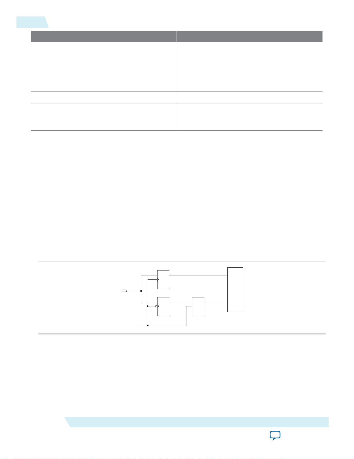
D Q
DFF
D Q
LATCH
ENA
D Q
DFF
INPUT
datain
inclock
neg_reg_out
dataout_l
dataout_h
Input Register A
Input Register B
Latch C
Latch
Logic
Array
I
I
I
6
ALTDDIO Functional Description
Parameter Description
Use ‘dqsundelayedout’ port Creates undelayed output from the DQS pins. If you
use the ALTDDIO_BIDIR IP core for your DQS
signal in an external memory interface, you route
the undelayed DQS signal to the LE, in Stratix II and
Stratix devices. This option is available in Stratix,
Stratix GX, and HardCopy Stratix devices only.
Use ‘dataout_h’ and ‘dataout_l’ ports Enables the dataout_h and dataout_l ports.
Implement input registers in LEs Implements the input path in logic elements. This
option is available only if the dataout_h and
dataout_l ports are enabled.
ALTDDIO Functional Description
DDR Device Configuration
The following sections describe how the DDR registers are configured in the Stratix series and APEX II
devices.
UG-DDRMGAFCTN
2015.01.23
Input Configuration
When the IOE is configured as an input pin, input registers AI and BI and latch CI implement the input
path for DDR I/O.
Figure 1: Input DDR I/O Path Configuration for a Stratix Series or APEX II Device
This figure shows an IOE configured for DDR inputs for a Stratix series or APEX II device.
Note:
On the falling edge of the clock, the negative-edge triggered register BI acquires the first data bit.
On the corresponding rising edge of the clock, the positive-edge triggered register AI acquires the
second data bit. For a successful data transfer to the logic array, the latch CI synchronizes the data
from register BI to the positive edge of the clock.
Altera Corporation
Double Data Rate I/O (ALTDDIO_IN, ALTDDIO_OUT, and ALTDDIO_BIDIR) IP Cores User Guide
Send Feedback
Page 7

CLRN/PRN
D Q
ENA
Chip-Wide Reset
Input Register
CLRN/PRN
D Q
ENA
Input Register
VCCIO
VCCIO
PCI Clamp
Programmable
Pull-Up
Resistor
Column, Row,
or Local
Interconnect
DQS Local
Bus
To DQS Logic
Block
ioe_clk[7..0]
Bus-Hold
Circuit
CLRN/PRN
D Q
ENA
Latch
Input Pin to
Input RegisterDelay
sclr/spreset
clkin
aclr/apreset
On-Chip
Termination
ce_in
(2)
(3)
(4)
1) All input signals to the IOE can be inverted at the IOE.
2) This signal connection is only allowed on dedicated DQ function pins.
3) This signal is for dedicated DQS function pins only.
4) The optional PCI clamp is only available on column I/O pins.
UG-DDRMGAFCTN
2015.01.23
Figure 2: Stratix II IOE in DDR Input I/O Configuration
Output Configuration
This figure shows an IOE configured for DDR inputs for a Stratix or Stratix II device.
7
Output Configuration
The dedicated output registers for Stratix series and APEX II devices are labeled AO and BO. These
positive-edge triggered registers and a multiplexer are used to implement the output path for DDR I/O.
Double Data Rate I/O (ALTDDIO_IN, ALTDDIO_OUT, and ALTDDIO_BIDIR) IP Cores User Guide
Send Feedback
Altera Corporation
Page 8

OUTPUT
Logic Array
outclock
datain_h
datain_l
D Q
DFF
D Q
DFF
0
1
Output Reg Ao
Output Reg Bo
D Q
DFF
D Q
DFF
OR2
TRI
dataout
OE Reg B
OE
OE Reg A
OE
0
1
(1)
OE
(2)
(4)
(3)
(5)
1) The OE is active low, but the Quartus II software implements this as active high and automatically adds an inverter before the input to the AOE
register during compilation. If desired, you can change the OE back to active low.
2) Register AOE generates the enable signal for general-purpose DDR I/O applications.
3) This select line corresponds to the delay switch-on by a half clock cycle option in the Parameter Editor.
4) Register BOE generates the delayed enable signal for DDR SDRAM applications.
5) The tri-state is active high by default. However, you can design it to be active low.
8
Output Configuration
Figure 3: Output DDR I/O Path Configuration for Stratix Series and APEX II Devices
This figure shows the IOE configuration for DDR outputs in Stratix series and APEX II devices.
UG-DDRMGAFCTN
2015.01.23
On the positive edge of the clock, a high data bit and a low data bit are captured in registers AO and BO.
The outputs of these two registers are fed to the input of a 2-to-1 multiplexer, which uses the output
register clock as its control signal. A high clock selects the data in register BO, and a low level of the clock
selects the data in register AO. This process doubles the data at the I/O pin.
Altera Corporation
Double Data Rate I/O (ALTDDIO_IN, ALTDDIO_OUT, and ALTDDIO_BIDIR) IP Cores User Guide
Send Feedback
Page 9

CLRN/PRN
D Q
ENA
Chip-Wide Reset
OE Register
CLRN/PRN
D Q
ENA
OE Register
CLRN/PRN
D Q
ENA
Output Register
V
CCIO
V
CCIO
Optional
PCI Clamp
Programmable
Pull-Up
Resistor
Column or Row
Interconnect
I/O Interconnect
[15..0]
IOE_CLK[7..0]
Bus-Hold
Circuit
Logic Array
to Output
Register Delay
Output
tZX Delay
OE Register
tCO Delay
CLRN/PRN
D Q
ENA
Output Register
Logic Array
to Output
Register Delay
Drive Strength Control
Open-Drain Output
Slew Control
Used for
DDR SDRAM
clk
sclr
aclr/prn
clkout
Output
Pin Delay
Output
Enable Clock
Enable Delay
Output Clock
Enable Delay
UG-DDRMGAFCTN
2015.01.23
Figure 4: Stratix IOE in DDR Output I/O Configuration
Bidirectional Configuration
This figure shows the IOE configuration for DDR outputs in Stratix series devices
9
Bidirectional Configuration
Input and output registers are independent of each other, enabling the bidirectional DDR I/O path to be
implemented entirely in the I/O element for Stratix, Stratix GX, and APEX II devices. The bidirectional
configuration includes an input path, an output path, and two output enable registers.
Double Data Rate I/O (ALTDDIO_IN, ALTDDIO_OUT, and ALTDDIO_BIDIR) IP Cores User Guide
The bidirectional path consists of two data flow paths:
• Input path active
• Output path active
When the input path is active, the output enable disables the tri-state buffer, which prevents data from
being sent out on the output path. Disabling the tri-state buffer prevents contention at the I/O pin. The
input path behaves like the input configuration as shown in Figure 3–1 on page 3–1. When the output
path is active, the output enable register AOE controls the flow of data from the output registers. During
outgoing transactions, the bidirectional configuration behaves like the output configuration as shown in
Figure 3–3 on page 3–3. The second output enable register (BOE) is used for DDR SDRAM interfaces. This
negative-edge register extends the high-impedance state of the pin by a half clock cycle. This option is
useful to provide the write preamble for the DQS strobe in the DDR SDRAM interfaces. This feature is
enabled by using the Delay switch-on by a half clock cycle option in the ALTDDIO_BIDIR IP core in the
Quartus II software. You can bypass the input registers and latch to get a combinational output (combout)
from the pin going into the APEX II or Stratix series device. Furthermore, the input data ports
Send Feedback
Altera Corporation
Page 10

DQ
DFF
DQ
ENA
DQ
DFF
Input Register B
I
Input Register A
I
Latch C
D Q
DFF
D Q
DFF
0
1
Output Register A
O
Output Register B
O
D Q
DFF
D Q
DFF
OR2
TRI
I/O Pin (7)
OE Register B
OE
OE Register A
OE
Logic Array
dataout_l
dataout_h
outclock
datain_h
datain_l
OE
inclock
neg_reg_out
I
0
(5)
(4)
(6)
(3)
combout
1
(2)
Latch
TCHLA
1) All control signals can be inverted at the IOE.
2) The OE signal is active low, but the Quartus II software implements this as active high and automatically adds an inverter before input to the AOE
register during compilation. If desired, you can change the OE back to active low.
3) The AOE register generates the enable signal for general-purpose DDR I/O applications.
4)This line selects whether the OE signal should be delayed by half a clock cycle.
5) The BOE register generates the delayed enable signal for the write strobes or write clocks for memory interfaces.
6) The tri-state enable is by default active low. You can, however, design it to be active high.
7) You can also have combinational output to the I/O pin. This path is not shown in the diagram.
10
Bidirectional Configuration
(dataout_h and dataout_l) can be disabled. These features are especially useful for generating data
strobes like DQS.
Figure 5: Bidirectional DDR I/O Path Configuration
This figure shows the bidirectional DDR I/O configuration for Stratix series and APEX II devices.
UG-DDRMGAFCTN
2015.01.23
Related Information
• Stratix II Architecture
For more information about clock signals and output enable signals for Stratix series
• APEX II Programmable Logic Device Family Data Sheet
For more information about clock signals and output enable signals for APEX II devices
• Implementing Double Data Rate I/O Signaling in Cyclone Devices
For more information about the DDR registers in Cyclone devices
Altera Corporation
Double Data Rate I/O (ALTDDIO_IN, ALTDDIO_OUT, and ALTDDIO_BIDIR) IP Cores User Guide
Send Feedback
Page 11

inclock
datain
dataout_h
dataout_l
E0 E1 E2
D0 D1 D2
XX
XX
D0 D1 D2
E0D0 E1D1 E2D2
D3
D3XX
neg_reg_out
outclock
datain_l
dataout
datain_h
OE
D1 E1 D3 E3D2 E2D0 E0
ZZ
ZZ
D0 D1 D2 D3XX XX
E0 E1 E2 E3
XX
XX
UG-DDRMGAFCTN
2015.01.23
DDR I/O Timing
Figure 6: DDR I/O Input Timing Waveform
DDR I/O Timing
11
• Implementing Double Data Rate I/O Signaling in Cyclone Devices
For more information about the DDR registers in Cyclone devices
This figure shows the functional timing waveform for the input path. The signal names are the port names
used in the ALTDDIO_IN IP core. The datain signal is the input from the pin to the DDR circuitry. The
output of register BI is neg_reg_out. The output of latch CI is dataout_1, and the output of register AI is
dataout_h. dataout_h and dataout_l feed the logic array and show the conversion of the data from a
DDR implementation to positive-edge triggered data.
This figure shows a functional timing waveform example for the output path with the output enable
registered. In this example, the delay switch-on by a half clock cycle is not turned on, so the second
output enable register (BOE) is not used. The output enable signal OE is active high and can be driven
from a pin or internal logic. The data signals datain_l and datain_h are driven from the logic array to
output registers AO and BO. The dataout signal is the output from the DDR circuitry to the pin.
Figure 7: DDR I/O Output Timing Waveform
The waveform in this figure reflects the software simulation results. The OE signal is active low in silicon;
however, the Quartus II software implements this as active high and automatically adds an inverter before
the D input of the OE register AOE. You can change the OE back to active low, if desired.
Double Data Rate I/O (ALTDDIO_IN, ALTDDIO_OUT, and ALTDDIO_BIDIR) IP Cores User Guide
Send Feedback
Altera Corporation
Page 12

12
Design Example 2: 8-Bit DDR Divider Using ALTDDIO_BIDIR
Design Example 2: 8-Bit DDR Divider Using ALTDDIO_BIDIR
This section presents a design example that uses the ALTDDIO_BIDIR IP core to generate a divider.
When you are finished with this example, you can incorporate it into your overall project.
In this example, you perform the following tasks:
• Create a divider using the ALTDDIO_BIDIR and lpm_divide megafunctions and the MegaWizard
Plug-in Manager
• Implement the design and assign the Stratix EP1S10F780C6 device to the project
• Compile and simulate the design
Generate a Divider Using ALTDDIO_BIDIR
The new megafunction created in this example is added to the top-level file in your Quartus II project.
Create the ALTDDIO_BIDIR Module
Follow these steps to create the ALTDDIO_BIDIR module:
1. Unzip the ALTDDIO_DesignExample_ex2.zip file to any working directory on your PC.
2. In the Quartus II software, open the ex2.qar project .
3. On the Tools menu, select MegaWizard Plug-In Manager.
4. In the MegaWizard Plug-In manager dialog box, select Create a new custom megafunction variation,
and click Next. The MegaWizard Plug-In Manager page displays.
5. In the MegaWizard Plug-In Manager pages, select or verify the configuration settings shown in this
table. Click Next to advance from one page to the next.
UG-DDRMGAFCTN
2015.01.23
Parameter
Editor Page
2a
Parameter Value
Which megafunction would you like to customize In the I/O folder, select
ALTDDIO_BIDIR
Which device family will you be using? Stratix
Which type of output file do you want to create? VHDL
What name do you want for the output file? alt_bid
Return to this page for another create operation Turned off
Altera Corporation
Double Data Rate I/O (ALTDDIO_IN, ALTDDIO_OUT, and ALTDDIO_BIDIR) IP Cores User Guide
Send Feedback
Page 13

UG-DDRMGAFCTN
2015.01.23
Create the ALTDDIO_BIDIR Module
13
Parameter
Editor Page
3
Parameter Value
Currently selected device family Stratix IV
Match project/default Turned on
Width: (bits) 8
Use ‘aclr’ port Turned off
Use ‘aset’ port Turned off
Not used Turned on
Registers power up high Turned off
Use ‘sclr’ port Turned off
Use ‘sset’ port Turned off
Not used Turned on
Invert ‘padio’ port Turned off
Use ‘inclocken’ and ‘outclocken’ ports Turned off
Use output enable port Turned on
Use ‘oe_out’ port to connect to tri-state output buffer(s) Turned off
Register ‘oe’ port Turned off
4
Delay switch-on by half a clock cycle Turned off
Use ‘combout’ port Turned off
Use ‘dqsundelayedout’ port Turned off
Use ‘dataout_h’ and ‘dataout_l” ports Turned on
Implement input registers in LEs Turned off
5 Generate netlist Turned off
Variation file Turned on
Quartus II IP file Turned on
Quartus II symbol file (.bsf) Turned off
Instantiation template file Turned on
6
Verilog HDL black box file (_bb.v) Turned on
AHDL Include file (.inc) Turned off
VHDL component declaration file (.cmp) Turned on
PinPlanner ports file (.PPF) Turned on
6. Click Finish.
The ALTDDIO_BIDIR module is now built.
Double Data Rate I/O (ALTDDIO_IN, ALTDDIO_OUT, and ALTDDIO_BIDIR) IP Cores User Guide
Send Feedback
Altera Corporation
Page 14

14
Create the LPM_DIVIDE Module
Related Information
Design Example 2: 8-Bit DDR Divider Using ALTDDIO_BIDIR
Create the LPM_DIVIDE Module
Follow these steps to create the lpm_divide module:
1. On the Tools menu, select MegaWizard Plug-In Manager.
2. In the MegaWizard Plug-In manager dialog box, select Create a new custom megafunction variation,
and click Next. The MegaWizard Plug-In Manager page displays.
3. In the MegaWizard Plug-In Manager pages, select or verify the configuration settings shown in this
table. Click Next to advance from one page to the next.
Parameter Editor Page Parameter Value
UG-DDRMGAFCTN
2015.01.23
2a
3
Which megafunction
would you like to
In the Arithmetic folder, select
LPM_DIVIDE
customize
Which device family will
Stratix
you be using?
Which type of output file
VHDL
do you want to create?
What name do you want
lp_div
for the output file?
Return to this page for
Turned off
another create operation
Currently selected device
Stratix IV
family
Match project/default Turned on
How wide should the
8
‘numerator’ input bus be?
How wide should the
8
‘denominator’ input bus
be?
Altera Corporation
Numerator Representa‐
Select Unsigned
tion
Denominator Represen‐
Select Unsigned
tation
Double Data Rate I/O (ALTDDIO_IN, ALTDDIO_OUT, and ALTDDIO_BIDIR) IP Cores User Guide
Send Feedback
Page 15
UG-DDRMGAFCTN
2015.01.23
Create a Divider
Parameter Editor Page Parameter Value
15
Do you want to pipeline
the function?
Create an Asynchronous
Select Yes, I want an output latency
of 1 clock cycle
Turned off
Clear input
4
Create a Clock Enable
input
Which do you wish to
Turned off
Select Default Optimization
optimize?
Always return a positive
Select Yes
remainder?
5 Generate netlist Turned off
Variation file Turned on
Quartus II IP file Turned on
Quartus II symbol file
Turned off
(.bsf)
Instantiation template
Turned on
file
6
Verilog HDL black box
Turned on
file (_bb.v)
4.
Click Finish.
The lpm_divide module is now built.
Create a Divider
Use the following steps to combine the ALTDDIO_BIDIR and lpm_divide modules to create a divider.
Follow these steps to create a top-level VHDL file:
1. In the Quartus II software, with the ex2.qar project open, open the file ex2.vhd.
2. On the Project menu, click Add/Remove File in Project. The File Settings page displays.
3. In the File Settings window, click (...) after File name and browse for ex2.vhd in the project folder.
4. Select ex2.vhd and click Add.
5. Click OK.
The top-level file is added to the project. You have now created the complete design file.
AHDL Include file (.inc) Turned off
VHDL component
Turned on
declaration file (.cmp)
PinPlanner ports file
Turned on
(.PPF)
Double Data Rate I/O (ALTDDIO_IN, ALTDDIO_OUT, and ALTDDIO_BIDIR) IP Cores User Guide
Send Feedback
Altera Corporation
Page 16

16
Implement the Divider Design
This design implements the same divider as that in Design Example 1, but the functionality of the
ALTDDIO_IN and ALTDDIO_OUT modules is implemented in a single megafunction, ALTDDIO_BIDIR.
The bidirectional pins DDR_BIDIR8[7..0] receive data at double the clock rate. The
DDRBIDIR8_OUT_H[7..0] signals are the numerator and the DDRBIDIR8_OUT_L[7..0] signals are the
denominator. These two sets of signals are passed to the lpm_divide module where the quotient and
remainder are calculated. The divider calculates the quotient and remainder with a one-stage pipeline.
The quotient and remainder are then fed via signals quotient[7..0] and remain[7..0] back to the
ALTDDIO_BIDIR megafunction. The ALTDDIO_BIDIR megafunction then drives the data out
through pins DDR_BIDIR8[7..0] at double the data rate.
Implement the Divider Design
This section describes how to assign the Stratix EP1S10F780C6 device to the project and compile the
project.
1. With the ex2.qar project open, on the Assignments menu, click Settings. The Settings dialog box
displays.
2. In the Category list, select Device.
3. To answer Which device family will you be using?, select Stratix.
4. Under Target device, select Specific device selected in ‘Available devices’ list.
5. In the Available devices list, select EP1S10F780C6.
6. Under Show in ‘Available devices’ list, select FBGA as the Package, Pin count of 780, Speed grade of
6, and turn on Show Advanced Devices.
7. Click OK.
8. On the Processing menu, click Start Compilation.
9. When the Full Compilation was successful box displays, click OK.
UG-DDRMGAFCTN
2015.01.23
Functional Results—Simulate the Divider Design in the ModelSim-Altera Software
Simulate the design in the ModelSim-Altera software to generate a waveform display of the device
behavior.
To set up the ModelSim-Altera software, follow these steps:
1. Unzip the ALTDDIO_ex2_msim.zip file to any working directory on your PC.
2. Browse to the folder in which you unzipped the files and open the ALTDDIO_ex2.do file in a text
editor.
3. In line 1 of the ALTDDIO_ex2.do file, replace <insert_directory_path_here> with the directory path
of the appropriate library files. For example, C:/altera/71/modelsim_ae/altera/verilog/stratix
4. On the File menu, click Save.
5. Start ModelSim-Altera.
6. On the File menu, click Change Directory.
7. Select the folder in which you unzipped the files. Click OK.
8. On the Tools menu, click Execute Macro.
9. Select the ALTDDIO_ex2.do file and click Open. This is a script file for ModelSim that automates all
the necessary settings for the simulation.
10.Verify the results by looking at the Waveform Viewer window.
You can rearrange signals, remove redundant signals, and change the radix by modifying the script in
the ALTDDIO_ex2.do file.
Altera Corporation
Double Data Rate I/O (ALTDDIO_IN, ALTDDIO_OUT, and ALTDDIO_BIDIR) IP Cores User Guide
Send Feedback
Page 17
datain[ ]
inclock
inclocken
aclr
aset
dataout_h[ ]
dataout_l[ ]
altddio_in
UG-DDRMGAFCTN
2015.01.23
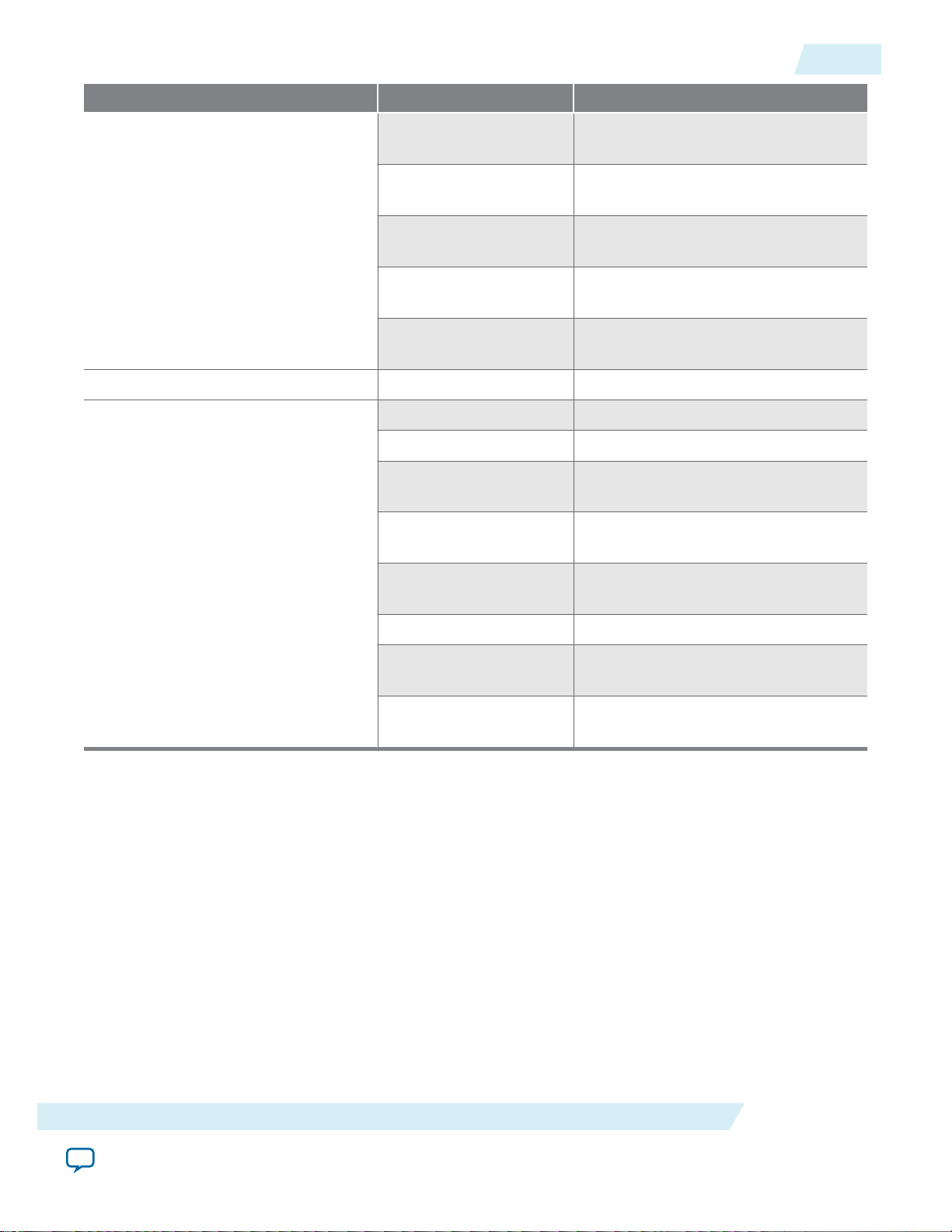
Figure 8: ModelSim Simulation Results
This figure shows the expected simulation results in ModelSim-Altera software.
Related Information
Divider Design in the ModelSim Simulation
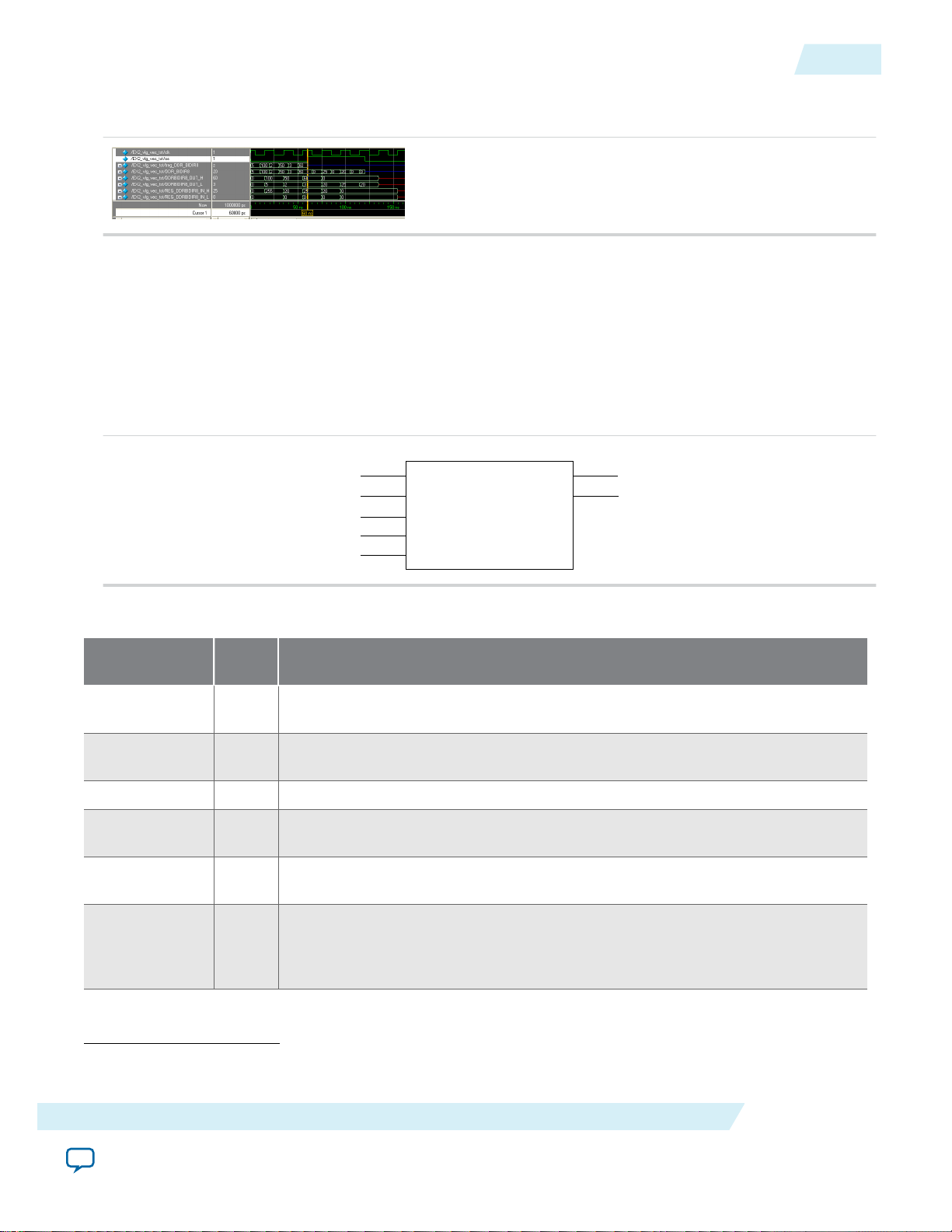
ALTDDIO_IN IP Core Signals
These tables list the input and output ports for the ALTDDIO_IN IP core.
Figure 9: ALTDDIO_IN Ports
ALTDDIO_IN IP Core Signals
17
Table 4: ALTDDIO_IN Input Ports
Name
datain[] Yes DDR input data port. Input port WIDTH wide. The datain port should be directly
Require
d
Description
fed from an input pin in the top-level design.
inclock Yes Clock signal to sample the DDR input. The datain port is sampled on each clock
edge of the inclock signal.
inclocken No Clock enable for the data clock
aclr No Asynchronous clear input. The aclr and aset ports cannot be connected at the
same time.
aset No Asynchronous set input. The aclr and aset ports cannot be connected at the
same time.
sclr No Synchronous clear input. The sclr and sset ports cannot be connected at the
same time. The sclr port is available for Arria GX, Stratix III, Stratix II,
Stratix II GX, Stratix, Stratix GX, HardCopy II, and HardCopy Stratix devices
(1)
only.
(1)
When designing with Stratix III devices, when sclr is asserted, it synchronously presets both the input
path and resynchronization register.
Double Data Rate I/O (ALTDDIO_IN, ALTDDIO_OUT, and ALTDDIO_BIDIR) IP Cores User Guide
Send Feedback
Altera Corporation
Page 18
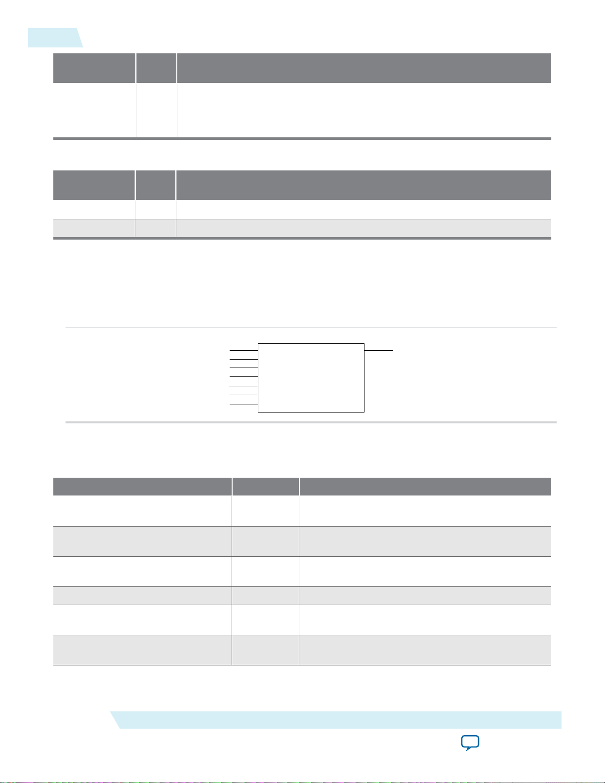
datain_h[ ]
outclock
outclocken
aclr
aset
dataout[ ]
altddio_out
datain_l[ ]
oe
18
ALTDDIO_OUT IP Core Signals
UG-DDRMGAFCTN
2015.01.23
Name
sset No Synchronous set input. The sclr and sset ports cannot be connected at the
Require
d
Description
same time. The sset port is available for Arria GX, Stratix III, Stratix II,
Stratix II GX, Stratix, Stratix GX, HardCopy II, and HardCopy Stratix devices
(1)
only.
Table 5: ALTDDIO_IN Output Ports
Name Require
d
dataout_h[] Yes Data sampled from datain[] port at the rising edge of the inclock signal.
dataout_l[] Yes Data sampled from datain[] port at the falling edge of the inclock signal.
Description
ALTDDIO_OUT IP Core Signals
This figure shows the ports for the ALTDDIO_OUT IP core.
Figure 10: ALTDDIO_OUT Signals
These tables list the input and output ports for the ALTDDIO_OUT IP core.
Table 6: ALTDDIO_OUT Input Ports
Name Required Description
datain_h[] Yes Input data for rising edge of outclock port. Input
datain_l[] Yes Input data for falling edge of outclock port. Input
outclock Yes Clock signal to register data output. dataout port
outclocken No Clock enable for outclock port.
aclr No Asynchronous clear input. The aclr and aset ports
aset No Asynchronous set input. The aclr and aset ports
Altera Corporation
port WIDTH wide.
port WIDTH wide.
outputs DDR data on each level of outclock signal.
cannot be connected at the same time.
cannot be connected at the same time.
Double Data Rate I/O (ALTDDIO_IN, ALTDDIO_OUT, and ALTDDIO_BIDIR) IP Cores User Guide
Send Feedback
Page 19

datain_h[ ]
inclock
inclocken
outclocken
oe
dataout_h[ ]
altddio_bidir
datain_l[ ]
outclock
dataout_l[ ]
padio[ ]
combout[ ]
dqsundelayedout[ ]
UG-DDRMGAFCTN
2015.01.23
Name Required Description
oe No Output enable for the dataout port. Active-high
sclr No Synchronous clear input. The sclr and sset ports
sset No Synchronous set input. The sclr and sset ports
Table 7: ALTDDIO_OUT Output Ports
Name Required Description
dataout[] Yes DDR output data port. Output port WIDTH wide.
ALTDDIO_BIDIR IP Core Signals
signal. You can add an inverter if you need an activelow oe.
cannot be connected at the same time. The sclr port
is available for Arria GX, Stratix III, Stratix II,
Stratix II GX, Stratix, Stratix GX, HardCopy II, and
HardCopy Stratix devices only.
cannot be connected at the same time. The sset port
is available for Arria GX, Stratix III, Stratix II,
Stratix II GX, Stratix, Stratix GX, HardCopy II, and
HardCopy Stratix devices only.
dataout port should directly feed an output pin in
top-level design.
19
oe_out No Output enable for the bidirectional padio port.
Output port [WIDTH–1..0] wide. This port is available
for Stratix III and Cyclone III devices only.
ALTDDIO_BIDIR IP Core Signals
This figure shows the ports for the ALTDDIO_BIDIR IP core.
Figure 11: ALTDDIO_BIDIR Ports
These tables list the output ports and the bidirectional ports for the ALTDDIO_BIDIR IP core.
Table 8: ALTDDIO_BIDIR Input Ports
Name Required Description
datain_h[] Yes Input data to be output to the padio port at the rising
edge of the outclock port. Input port [(WIDTH) - (1)
..0] wide.
Double Data Rate I/O (ALTDDIO_IN, ALTDDIO_OUT, and ALTDDIO_BIDIR) IP Cores User Guide
Send Feedback
Altera Corporation
Page 20
20
ALTDDIO_BIDIR IP Core Signals
Name Required Description
datain_l[] Yes Input data to be output to the padio port at the falling
edge of the outclock port. Input port [(WIDTH) - (1)
..0] wide.
inclock Yes Clock signal to sample the DDR input. The padio port is
sampled on each clock edge of the inclock signal.
inclocken No Clock enable for the inclock port.
outclock Yes Clock signal to register the data output. The padio port
outputs the DDR data on each edge of the outclock
signal.
outclocken No Clock enable for the outclock port.
aclr No Asynchronous clear input. The aclr and aset ports
cannot be connected at the same time.
aset No Asynchronous set input. The aclr and aset ports
cannot be connected at the same time.
oe No Output enable for the bidirectional padio port. If the oe
port is not connected, then the padio port is an output
port.
UG-DDRMGAFCTN
2015.01.23
sclr No Synchronous clear input. The sclr and sset ports
cannot be connected at the same time. The sclr port is
available for Arria GX, Stratix III, Stratix II,
Stratix II GX, Stratix, Stratix GX, HardCopy II, and
HardCopy Stratix devices only.
sset No Synchronous set input. The sclr and sset ports cannot
(2)
be connected at the same time. The sset port is
available for Arria GX, Stratix III, Stratix II,
Stratix II GX, Stratix, Stratix GX, HardCopy II, and
HardCopy Stratix devices only.
(2)
Table 9: ALTDDIO_BIDIR Output Ports
Name Required Description
dataout_h[] Yes Data sampled from the padio port at the rising edge of
the inclock signal. Output port [WIDTH–1..0] wide.
dataout_l[] Yes Data sampled from the padio port at the falling edge of
the inclock signal. Output port [WIDTH-1..0] wide.
combout[](1) No Combinational output directly fed by the padio port.
dqsundelayedout[] No Undelayed output from the DQS pins. Output port
[WIDTH-1..0] wide.
(4)
(3)
(2)
When designing with Stratix III devices, when sclr is deasserted, it synchronously presents both the
input path and resynchronization register.
(3)
This port is available for Stratix series, HardCopy Stratix, Cyclone series, and APEX II devices only.
(4)
This port is available for Stratix and HardCopy Stratix devices only.
Altera Corporation
Double Data Rate I/O (ALTDDIO_IN, ALTDDIO_OUT, and ALTDDIO_BIDIR) IP Cores User Guide
Send Feedback
Page 21
UG-DDRMGAFCTN
2015.01.23
Name Required Description
oe_out No Output enable for the bidirectional padio port. Output
Table 10: ALTDDIO_BIDIR Bidirectional Port
Name Required Description
padio[] Yes Bidirectional DDR port that should directly feed a
Verilog HDL Prototype
The Verilog HDL prototype is located in the <Quartus II installation directory>\eda\synthesis\ altera_mf.v
Verilog HDL Prototype
port [WIDTH–1..0] wide. This port is available for
Stratix III and Cyclone III devices only.
bidirectional pin in the top-level design. The DDR data
is transmitted and received on this bidirectional port.
Bidirectional port [(WIDTH) - (1)..0] wide.
21
VHDL Component Declaration
You can locate VHDL component declaration in the VHDL Design File (.vhd)
altera_mf_components.vhd in the <Quartus II installation directory>\libraries\vhdl\altera_mf
directory.
VHDL LIBRARY-USE Declaration
The VHDL LIBRARY-USE declaration is not required if you use the VHDL Component Declaration.
LIBRARY altera_mf;
USE altera_mf.altera_mf_components.all;
Document Revision History
The following table lists the revision history for this document.
Table 11: Document Revision History
Date Version Changes
January 2015 2015.01.23 Added link to design example file.
December 2014 2014.12.15 Template update.
January 2013 6.1 Updated to correct content error in “DDR I/O
Timing” on page 3–7.
February 2012 6.0 Updated to refelect new GUI changes.
Double Data Rate I/O (ALTDDIO_IN, ALTDDIO_OUT, and ALTDDIO_BIDIR) IP Cores User Guide
Send Feedback
Altera Corporation
Page 22

22
Document Revision History
Date Version Changes
September 2010 5.0 Added ports and parameters.
June 2007 4.2 Updated for Quartus II software version 7.1:
• Updated for Arria GX and Cyclone III devices.
• Updated and renamed “DDR MegaWizard PlugIns Page Descriptions” section.
• Added parameter to the ALTDDIO_IN megafunc‐
tion.
• Added “Referenced Documents” section.
Updated “Revision History” and “How to Contact
Altera” sections.
March 2007 4.1 Added Cyclone III device to list of supported devices.
July 2006 4.0 Updated to reflect Quartus II 6.0 release, added
ModelSim simulation information, updated design
examples.
March 2005 3.0 Updated to reflect new GUI changes.
UG-DDRMGAFCTN
2015.01.23
December 2004 2.0 Updated to reflect new document organization and
GUI changes.
Altera Corporation
Double Data Rate I/O (ALTDDIO_IN, ALTDDIO_OUT, and ALTDDIO_BIDIR) IP Cores User Guide
Send Feedback
 Loading...