

Page 1

13.1CPRI MegaCore Function User Guide
CPRI MegaCore Function
User Guide
101 Innovation Drive
San Jose, CA 95134
www.altera.com
UG-01062-6.3
Document last updated for Altera Complete Design Suite version:
Document publication date:
13.1
December 2013
Feedback Subscribe
Page 2

© 2013 Altera Corporation. All rights reserved. ALTERA, ARRIA, CYCLONE, HARDCOPY, MAX, MEGACORE, NIOS, QUARTUS and STRATIX words and logos
are trademarks of Altera Corporation and registered in the U.S. Patent and Trademark Office and in other countries. All other words and logos identified as
trademarks or service marks are the property of their respective holders as described at www.altera.com/common/legal.html. Altera warrants performance of its
semiconductor products to current specifications in accordance with Altera's standard warranty, but reserves the right to make changes to any products and
services at any time without notice. Altera assumes no responsibility or liability arising out of the application or use of any information, product, or service
described herein except as expressly agreed to in writing by Altera. Altera customers are advised to obtain the latest version of device specifications before relying
on any published information and before placing orders for products or services.
ISO
9001:2008
Registered
December 2013 Altera Corporation CPRI MegaCore Function
User Guide
Page 3

Contents
Chapter 1. About This MegaCore Function
General Description . . . . . . . . . . . . . . . . . . . . . . . . . . . . . . . . . . . . . . . . . . . . . . . . . . . . . . . . . . . . . . . . . . . . . 1–2
CPRI IP Core Features . . . . . . . . . . . . . . . . . . . . . . . . . . . . . . . . . . . . . . . . . . . . . . . . . . . . . . . . . . . . . . . . . . . 1–3
Device Family Support . . . . . . . . . . . . . . . . . . . . . . . . . . . . . . . . . . . . . . . . . . . . . . . . . . . . . . . . . . . . . . . . . . . 1–5
MegaCore Verification . . . . . . . . . . . . . . . . . . . . . . . . . . . . . . . . . . . . . . . . . . . . . . . . . . . . . . . . . . . . . . . . . . . 1–6
Performance and Resource Utilization . . . . . . . . . . . . . . . . . . . . . . . . . . . . . . . . . . . . . . . . . . . . . . . . . . . . . . 1–6
Release Information . . . . . . . . . . . . . . . . . . . . . . . . . . . . . . . . . . . . . . . . . . . . . . . . . . . . . . . . . . . . . . . . . . . . . 1–8
Installation and Licensing . . . . . . . . . . . . . . . . . . . . . . . . . . . . . . . . . . . . . . . . . . . . . . . . . . . . . . . . . . . . . . . . 1–9
OpenCore Plus Evaluation . . . . . . . . . . . . . . . . . . . . . . . . . . . . . . . . . . . . . . . . . . . . . . . . . . . . . . . . . . . . 1–10
OpenCore Plus Time-Out Behavior . . . . . . . . . . . . . . . . . . . . . . . . . . . . . . . . . . . . . . . . . . . . . . . . . . . . . 1–10
Chapter 2. Getting Started
MegaWizard Plug-In Manager Design Flow . . . . . . . . . . . . . . . . . . . . . . . . . . . . . . . . . . . . . . . . . . . . . . . . 2–1
Specifying Parameters . . . . . . . . . . . . . . . . . . . . . . . . . . . . . . . . . . . . . . . . . . . . . . . . . . . . . . . . . . . . . . . . . 2–2
Simulation Files . . . . . . . . . . . . . . . . . . . . . . . . . . . . . . . . . . . . . . . . . . . . . . . . . . . . . . . . . . . . . . . . . . . . . . . 2–3
Simulating the Design . . . . . . . . . . . . . . . . . . . . . . . . . . . . . . . . . . . . . . . . . . . . . . . . . . . . . . . . . . . . . . . . . 2–4
Integrating the CPRI IP Core in a Design . . . . . . . . . . . . . . . . . . . . . . . . . . . . . . . . . . . . . . . . . . . . . . . . . . . 2–5
Supporting the Transceivers . . . . . . . . . . . . . . . . . . . . . . . . . . . . . . . . . . . . . . . . . . . . . . . . . . . . . . . . . . . . 2–5
Specifying Constraints . . . . . . . . . . . . . . . . . . . . . . . . . . . . . . . . . . . . . . . . . . . . . . . . . . . . . . . . . . . . . . . . . 2–5
Compiling and Programming the Device . . . . . . . . . . . . . . . . . . . . . . . . . . . . . . . . . . . . . . . . . . . . . . . . . . . 2–6
Instantiating Multiple CPRI IP Cores . . . . . . . . . . . . . . . . . . . . . . . . . . . . . . . . . . . . . . . . . . . . . . . . . . . . . . . 2–6
Chapter 3. Parameter Settings
Physical Layer Parameters . . . . . . . . . . . . . . . . . . . . . . . . . . . . . . . . . . . . . . . . . . . . . . . . . . . . . . . . . . . . . . . . 3–1
Operation Mode Parameter . . . . . . . . . . . . . . . . . . . . . . . . . . . . . . . . . . . . . . . . . . . . . . . . . . . . . . . . . . . . 3–2
Line Rate Parameter . . . . . . . . . . . . . . . . . . . . . . . . . . . . . . . . . . . . . . . . . . . . . . . . . . . . . . . . . . . . . . . . . . . 3–2
Enable Autorate Negotiation . . . . . . . . . . . . . . . . . . . . . . . . . . . . . . . . . . . . . . . . . . . . . . . . . . . . . . . . . . . 3–3
Transceiver Starting Channel Number . . . . . . . . . . . . . . . . . . . . . . . . . . . . . . . . . . . . . . . . . . . . . . . . . . . 3–3
Rx Elastic Buffer Depth . . . . . . . . . . . . . . . . . . . . . . . . . . . . . . . . . . . . . . . . . . . . . . . . . . . . . . . . . . . . . . . . 3–3
Transceiver Reference Clock Frequency . . . . . . . . . . . . . . . . . . . . . . . . . . . . . . . . . . . . . . . . . . . . . . . . . . 3–4
Automatic Round-Trip Delay Calibration . . . . . . . . . . . . . . . . . . . . . . . . . . . . . . . . . . . . . . . . . . . . . . . . 3–4
Data Link Layer Parameters . . . . . . . . . . . . . . . . . . . . . . . . . . . . . . . . . . . . . . . . . . . . . . . . . . . . . . . . . . . . . . 3–4
Include MAC Block . . . . . . . . . . . . . . . . . . . . . . . . . . . . . . . . . . . . . . . . . . . . . . . . . . . . . . . . . . . . . . . . . . . 3–4
Include HDLC Block . . . . . . . . . . . . . . . . . . . . . . . . . . . . . . . . . . . . . . . . . . . . . . . . . . . . . . . . . . . . . . . . . . 3–5
Application Layer Parameters . . . . . . . . . . . . . . . . . . . . . . . . . . . . . . . . . . . . . . . . . . . . . . . . . . . . . . . . . . . . . 3–5
Mapping Mode . . . . . . . . . . . . . . . . . . . . . . . . . . . . . . . . . . . . . . . . . . . . . . . . . . . . . . . . . . . . . . . . . . . . . . . 3–5
Number of Antenna-Carrier Interfaces . . . . . . . . . . . . . . . . . . . . . . . . . . . . . . . . . . . . . . . . . . . . . . . . . . . 3–6
Enable Internally-Clocked Synchronization Mode . . . . . . . . . . . . . . . . . . . . . . . . . . . . . . . . . . . . . . . . . 3–7
Vendor-Specific Space (VSS) Access through CPU Interface . . . . . . . . . . . . . . . . . . . . . . . . . . . . . . . . . 3–7
Chapter 4. Functional Description
Architecture Overview . . . . . . . . . . . . . . . . . . . . . . . . . . . . . . . . . . . . . . . . . . . . . . . . . . . . . . . . . . . . . . . . . . . 4–2
Clocking Structure . . . . . . . . . . . . . . . . . . . . . . . . . . . . . . . . . . . . . . . . . . . . . . . . . . . . . . . . . . . . . . . . . . . . . . . 4–3
CPRI IP Core Clocks . . . . . . . . . . . . . . . . . . . . . . . . . . . . . . . . . . . . . . . . . . . . . . . . . . . . . . . . . . . . . . . . . . . 4–3
Clock Diagrams for the CPRI IP Core . . . . . . . . . . . . . . . . . . . . . . . . . . . . . . . . . . . . . . . . . . . . . . . . . . . . 4–5
Clock Diagrams for Most CPRI IP Core Variations . . . . . . . . . . . . . . . . . . . . . . . . . . . . . . . . . . . . . . 4–6
Clock Diagrams for CPRI IP Core Arria V GT Variations at 9830.4 Mbps . . . . . . . . . . . . . . . . . . . 4–7
Dynamically Switching Clock Mode . . . . . . . . . . . . . . . . . . . . . . . . . . . . . . . . . . . . . . . . . . . . . . . . . . . . . 4–9
December 2013 Altera Corporation CPRI MegaCore Function
User Guide
Page 4

iv ContentsContents
CPRI Communication Link Line Rates . . . . . . . . . . . . . . . . . . . . . . . . . . . . . . . . . . . . . . . . . . . . . . . . . . 4–10
Reset Requirements . . . . . . . . . . . . . . . . . . . . . . . . . . . . . . . . . . . . . . . . . . . . . . . . . . . . . . . . . . . . . . . . . . . . . 4–11
MAP Interface . . . . . . . . . . . . . . . . . . . . . . . . . . . . . . . . . . . . . . . . . . . . . . . . . . . . . . . . . . . . . . . . . . . . . . . . . 4–12
MAP Interface Mapping Modes . . . . . . . . . . . . . . . . . . . . . . . . . . . . . . . . . . . . . . . . . . . . . . . . . . . . . . . . 4–13
Basic AxC Mapping Mode . . . . . . . . . . . . . . . . . . . . . . . . . . . . . . . . . . . . . . . . . . . . . . . . . . . . . . . . . . 4–14
Advanced AxC Mapping Modes . . . . . . . . . . . . . . . . . . . . . . . . . . . . . . . . . . . . . . . . . . . . . . . . . . . . . 4–18
MAP Receiver Interface . . . . . . . . . . . . . . . . . . . . . . . . . . . . . . . . . . . . . . . . . . . . . . . . . . . . . . . . . . . . . . . 4–18
MAP Receiver Interface Signals in Different Synchronization Modes . . . . . . . . . . . . . . . . . . . . . 4–19
MAP Receiver in FIFO Mode . . . . . . . . . . . . . . . . . . . . . . . . . . . . . . . . . . . . . . . . . . . . . . . . . . . . . . . . 4–20
MAP Receiver in Synchronous Buffer Mode . . . . . . . . . . . . . . . . . . . . . . . . . . . . . . . . . . . . . . . . . . . 4–21
MAP Receiver in the Internally-Clocked Mode . . . . . . . . . . . . . . . . . . . . . . . . . . . . . . . . . . . . . . . . 4–23
MAP Transmitter Interface . . . . . . . . . . . . . . . . . . . . . . . . . . . . . . . . . . . . . . . . . . . . . . . . . . . . . . . . . . . . 4–24
MAP Transmitter Interface Signals in Different Synchronization Modes . . . . . . . . . . . . . . . . . . 4–25
MAP Transmitter in FIFO Mode . . . . . . . . . . . . . . . . . . . . . . . . . . . . . . . . . . . . . . . . . . . . . . . . . . . . . 4–26
MAP Transmitter in Synchronous Buffer Mode . . . . . . . . . . . . . . . . . . . . . . . . . . . . . . . . . . . . . . . . 4–27
MAP Transmitter in the Internally-clocked Mode . . . . . . . . . . . . . . . . . . . . . . . . . . . . . . . . . . . . . . 4–29
Auxiliary Interface . . . . . . . . . . . . . . . . . . . . . . . . . . . . . . . . . . . . . . . . . . . . . . . . . . . . . . . . . . . . . . . . . . . . . 4–30
AUX Receiver Module . . . . . . . . . . . . . . . . . . . . . . . . . . . . . . . . . . . . . . . . . . . . . . . . . . . . . . . . . . . . . . . . 4–31
AUX Transmitter Module . . . . . . . . . . . . . . . . . . . . . . . . . . . . . . . . . . . . . . . . . . . . . . . . . . . . . . . . . . . . . 4–34
Media Independent Interface to an External Ethernet Block . . . . . . . . . . . . . . . . . . . . . . . . . . . . . . . . . . 4–37
MII Transmitter . . . . . . . . . . . . . . . . . . . . . . . . . . . . . . . . . . . . . . . . . . . . . . . . . . . . . . . . . . . . . . . . . . . . . . 4–38
MII Receiver . . . . . . . . . . . . . . . . . . . . . . . . . . . . . . . . . . . . . . . . . . . . . . . . . . . . . . . . . . . . . . . . . . . . . . . . 4–39
CPU Interface . . . . . . . . . . . . . . . . . . . . . . . . . . . . . . . . . . . . . . . . . . . . . . . . . . . . . . . . . . . . . . . . . . . . . . . . . . 4–41
Accessing the Hyperframe Control Words . . . . . . . . . . . . . . . . . . . . . . . . . . . . . . . . . . . . . . . . . . . . . . . 4–42
Recording and Retrieving the Incoming Control Words . . . . . . . . . . . . . . . . . . . . . . . . . . . . . . . . . 4–43
Writing the Outgoing Control Words . . . . . . . . . . . . . . . . . . . . . . . . . . . . . . . . . . . . . . . . . . . . . . . . 4–44
Control Word Order . . . . . . . . . . . . . . . . . . . . . . . . . . . . . . . . . . . . . . . . . . . . . . . . . . . . . . . . . . . . . . . 4–46
Control Word Transmission Example . . . . . . . . . . . . . . . . . . . . . . . . . . . . . . . . . . . . . . . . . . . . . . . . 4–46
Control Word Retrieval Example . . . . . . . . . . . . . . . . . . . . . . . . . . . . . . . . . . . . . . . . . . . . . . . . . . . . 4–47
Accessing the Ethernet Channel . . . . . . . . . . . . . . . . . . . . . . . . . . . . . . . . . . . . . . . . . . . . . . . . . . . . . . . . 4–47
Transmitting Ethernet Traffic . . . . . . . . . . . . . . . . . . . . . . . . . . . . . . . . . . . . . . . . . . . . . . . . . . . . . . . 4–48
Receiving Ethernet Traffic . . . . . . . . . . . . . . . . . . . . . . . . . . . . . . . . . . . . . . . . . . . . . . . . . . . . . . . . . . 4–49
Accessing the HDLC Channel . . . . . . . . . . . . . . . . . . . . . . . . . . . . . . . . . . . . . . . . . . . . . . . . . . . . . . . . . 4–50
CPRI Protocol Interface Layer (Physical Layer) . . . . . . . . . . . . . . . . . . . . . . . . . . . . . . . . . . . . . . . . . . . . . 4–51
Features . . . . . . . . . . . . . . . . . . . . . . . . . . . . . . . . . . . . . . . . . . . . . . . . . . . . . . . . . . . . . . . . . . . . . . . . . . . . 4–52
Physical Layer Architecture . . . . . . . . . . . . . . . . . . . . . . . . . . . . . . . . . . . . . . . . . . . . . . . . . . . . . . . . . . . 4–52
Ensuring the Physical Layer Routes Your Data as Expected . . . . . . . . . . . . . . . . . . . . . . . . . . . . . . . . 4–53
Receiver . . . . . . . . . . . . . . . . . . . . . . . . . . . . . . . . . . . . . . . . . . . . . . . . . . . . . . . . . . . . . . . . . . . . . . . . . . . . 4–53
High-Speed Transceiver . . . . . . . . . . . . . . . . . . . . . . . . . . . . . . . . . . . . . . . . . . . . . . . . . . . . . . . . . . . . 4–54
Rx Elastic Buffer . . . . . . . . . . . . . . . . . . . . . . . . . . . . . . . . . . . . . . . . . . . . . . . . . . . . . . . . . . . . . . . . . . . 4–54
Descrambling . . . . . . . . . . . . . . . . . . . . . . . . . . . . . . . . . . . . . . . . . . . . . . . . . . . . . . . . . . . . . . . . . . . . . 4–55
Frame Synchronization . . . . . . . . . . . . . . . . . . . . . . . . . . . . . . . . . . . . . . . . . . . . . . . . . . . . . . . . . . . . . 4–55
Alarm Indications . . . . . . . . . . . . . . . . . . . . . . . . . . . . . . . . . . . . . . . . . . . . . . . . . . . . . . . . . . . . . . . . . 4–56
Reset Control Word . . . . . . . . . . . . . . . . . . . . . . . . . . . . . . . . . . . . . . . . . . . . . . . . . . . . . . . . . . . . . . . . 4–57
Transmitter . . . . . . . . . . . . . . . . . . . . . . . . . . . . . . . . . . . . . . . . . . . . . . . . . . . . . . . . . . . . . . . . . . . . . . . . . 4–58
Scrambling . . . . . . . . . . . . . . . . . . . . . . . . . . . . . . . . . . . . . . . . . . . . . . . . . . . . . . . . . . . . . . . . . . . . . . . 4–59
Tx Elastic Buffer . . . . . . . . . . . . . . . . . . . . . . . . . . . . . . . . . . . . . . . . . . . . . . . . . . . . . . . . . . . . . . . . . . . 4–59
High-Speed Transceiver . . . . . . . . . . . . . . . . . . . . . . . . . . . . . . . . . . . . . . . . . . . . . . . . . . . . . . . . . . . . 4–59
Chapter 5. Testing Features
Loopback Modes . . . . . . . . . . . . . . . . . . . . . . . . . . . . . . . . . . . . . . . . . . . . . . . . . . . . . . . . . . . . . . . . . . . . . . . . 5–1
External Loopback . . . . . . . . . . . . . . . . . . . . . . . . . . . . . . . . . . . . . . . . . . . . . . . . . . . . . . . . . . . . . . . . . . . . 5–1
Internal Reverse Loopback . . . . . . . . . . . . . . . . . . . . . . . . . . . . . . . . . . . . . . . . . . . . . . . . . . . . . . . . . . . . . 5–2
Physical Layer Loopback Mode . . . . . . . . . . . . . . . . . . . . . . . . . . . . . . . . . . . . . . . . . . . . . . . . . . . . . . . 5–2
CPRI MegaCore Function December 2013 Altera Corporation
User Guide
Page 5

ContentsContents v
Reverse Loopback Through CPRI Rx and Tx Buffers . . . . . . . . . . . . . . . . . . . . . . . . . . . . . . . . . . . . 5–2
PRBS Generation and Validation . . . . . . . . . . . . . . . . . . . . . . . . . . . . . . . . . . . . . . . . . . . . . . . . . . . . . . . . . . 5–2
Achieving Link Synchronization Without an REC Master . . . . . . . . . . . . . . . . . . . . . . . . . . . . . . . . . . . . . 5–4
Chapter 6. Signals
MAP Interface Signals . . . . . . . . . . . . . . . . . . . . . . . . . . . . . . . . . . . . . . . . . . . . . . . . . . . . . . . . . . . . . . . . . . . 6–1
MAP Receiver Signals . . . . . . . . . . . . . . . . . . . . . . . . . . . . . . . . . . . . . . . . . . . . . . . . . . . . . . . . . . . . . . . . . 6–1
MAP Transmitter Signals . . . . . . . . . . . . . . . . . . . . . . . . . . . . . . . . . . . . . . . . . . . . . . . . . . . . . . . . . . . . . . 6–3
Auxiliary Interface Signals . . . . . . . . . . . . . . . . . . . . . . . . . . . . . . . . . . . . . . . . . . . . . . . . . . . . . . . . . . . . . . . . 6–5
AUX Receiver Signals . . . . . . . . . . . . . . . . . . . . . . . . . . . . . . . . . . . . . . . . . . . . . . . . . . . . . . . . . . . . . . . . . 6–6
AUX Transmitter Signals . . . . . . . . . . . . . . . . . . . . . . . . . . . . . . . . . . . . . . . . . . . . . . . . . . . . . . . . . . . . . . . 6–7
Extended Rx Status Signals . . . . . . . . . . . . . . . . . . . . . . . . . . . . . . . . . . . . . . . . . . . . . . . . . . . . . . . . . . . . . 6–9
CPRI MII Signals . . . . . . . . . . . . . . . . . . . . . . . . . . . . . . . . . . . . . . . . . . . . . . . . . . . . . . . . . . . . . . . . . . . . . . . 6–10
CPRI MII Receiver Signals . . . . . . . . . . . . . . . . . . . . . . . . . . . . . . . . . . . . . . . . . . . . . . . . . . . . . . . . . . . . 6–10
CPRI MII Transmitter Signals . . . . . . . . . . . . . . . . . . . . . . . . . . . . . . . . . . . . . . . . . . . . . . . . . . . . . . . . . . 6–10
CPU Interface Signals . . . . . . . . . . . . . . . . . . . . . . . . . . . . . . . . . . . . . . . . . . . . . . . . . . . . . . . . . . . . . . . . . . . 6–11
Physical Layer Signals . . . . . . . . . . . . . . . . . . . . . . . . . . . . . . . . . . . . . . . . . . . . . . . . . . . . . . . . . . . . . . . . . . 6–12
CPRI Data Signals . . . . . . . . . . . . . . . . . . . . . . . . . . . . . . . . . . . . . . . . . . . . . . . . . . . . . . . . . . . . . . . . . . . . 6–12
Layer 1 Clock and Reset Signals . . . . . . . . . . . . . . . . . . . . . . . . . . . . . . . . . . . . . . . . . . . . . . . . . . . . . . . . 6–13
Layer 1 Error Signal . . . . . . . . . . . . . . . . . . . . . . . . . . . . . . . . . . . . . . . . . . . . . . . . . . . . . . . . . . . . . . . . . . 6–13
Autorate Negotiation Signals . . . . . . . . . . . . . . . . . . . . . . . . . . . . . . . . . . . . . . . . . . . . . . . . . . . . . . . . . . 6–13
Transceiver Signals . . . . . . . . . . . . . . . . . . . . . . . . . . . . . . . . . . . . . . . . . . . . . . . . . . . . . . . . . . . . . . . . . . . 6–15
Clock and Reset Interface Signals . . . . . . . . . . . . . . . . . . . . . . . . . . . . . . . . . . . . . . . . . . . . . . . . . . . . . . . . . 6–17
Chapter 7. Software Interface
CPRI Protocol Interface Registers . . . . . . . . . . . . . . . . . . . . . . . . . . . . . . . . . . . . . . . . . . . . . . . . . . . . . . . . . . 7–2
MAP Interface and AUX Interface Configuration Registers . . . . . . . . . . . . . . . . . . . . . . . . . . . . . . . . . . . 7–15
Ethernet Registers . . . . . . . . . . . . . . . . . . . . . . . . . . . . . . . . . . . . . . . . . . . . . . . . . . . . . . . . . . . . . . . . . . . . . . 7–22
HDLC Registers . . . . . . . . . . . . . . . . . . . . . . . . . . . . . . . . . . . . . . . . . . . . . . . . . . . . . . . . . . . . . . . . . . . . . . . . 7–27
Chapter 8. CPRI IP Core Demonstration Testbench
Test Sequence . . . . . . . . . . . . . . . . . . . . . . . . . . . . . . . . . . . . . . . . . . . . . . . . . . . . . . . . . . . . . . . . . . . . . . . . . . . 8–3
Reset, Frame Synchronization, and Initialization . . . . . . . . . . . . . . . . . . . . . . . . . . . . . . . . . . . . . . . . . . . . . 8–4
Running the Testbench . . . . . . . . . . . . . . . . . . . . . . . . . . . . . . . . . . . . . . . . . . . . . . . . . . . . . . . . . . . . . . . . . . . 8–5
Appendix A. Initialization Sequence
Appendix B. Implementing CPRI Link Autorate Negotiation
Design Implementation . . . . . . . . . . . . . . . . . . . . . . . . . . . . . . . . . . . . . . . . . . . . . . . . . . . . . . . . . . . . . . . . . B–1
Configuring the CPRI IP Core for Autorate Negotiation . . . . . . . . . . . . . . . . . . . . . . . . . . . . . . . . . . . . . B–3
Running Autorate Negotiation . . . . . . . . . . . . . . . . . . . . . . . . . . . . . . . . . . . . . . . . . . . . . . . . . . . . . . . . . . . B–3
Autorate Negotiation From 9.8304 Gbps in Arria V GT Variations . . . . . . . . . . . . . . . . . . . . . . . . . . . . B–4
Appendix C. CPRI Autorate Negotiation Testbench
Test Sequence . . . . . . . . . . . . . . . . . . . . . . . . . . . . . . . . . . . . . . . . . . . . . . . . . . . . . . . . . . . . . . . . . . . . . . . . . . C–4
Running the Autorate Negotiation Testbench . . . . . . . . . . . . . . . . . . . . . . . . . . . . . . . . . . . . . . . . . . . . . . C–5
Appendix D. Advanced AxC Mapping Modes
Backward Compability . . . . . . . . . . . . . . . . . . . . . . . . . . . . . . . . . . . . . . . . . . . . . . . . . . . . . . . . . . . . . . . . . . D–1
Advanced Mapping Mode Similarities and Differences . . . . . . . . . . . . . . . . . . . . . . . . . . . . . . . . . . . . . . D–2
Fifteen-Bit Width Mode . . . . . . . . . . . . . . . . . . . . . . . . . . . . . . . . . . . . . . . . . . . . . . . . . . . . . . . . . . . . . . . D–3
Sixteen-Bit Width Mode . . . . . . . . . . . . . . . . . . . . . . . . . . . . . . . . . . . . . . . . . . . . . . . . . . . . . . . . . . . . . . D–4
December 2013 Altera Corporation CPRI MegaCore Function
User Guide
Page 6

vi ContentsContents
Appendix E. Delay Measurement and Calibration
Delay Measurement and Calibration Features . . . . . . . . . . . . . . . . . . . . . . . . . . . . . . . . . . . . . . . . . . . . . . E–1
Delay Requirements . . . . . . . . . . . . . . . . . . . . . . . . . . . . . . . . . . . . . . . . . . . . . . . . . . . . . . . . . . . . . . . . . . . . E–1
Single-Hop Delay Measurement . . . . . . . . . . . . . . . . . . . . . . . . . . . . . . . . . . . . . . . . . . . . . . . . . . . . . . . . . . E–3
Rx Path Delay . . . . . . . . . . . . . . . . . . . . . . . . . . . . . . . . . . . . . . . . . . . . . . . . . . . . . . . . . . . . . . . . . . . . . . . E–3
Most CPRI IP Core Variations . . . . . . . . . . . . . . . . . . . . . . . . . . . . . . . . . . . . . . . . . . . . . . . . . . . . . . . E–3
Arria V GT 9.8 Gbps . . . . . . . . . . . . . . . . . . . . . . . . . . . . . . . . . . . . . . . . . . . . . . . . . . . . . . . . . . . . . . E–10
Tx Path Delay . . . . . . . . . . . . . . . . . . . . . . . . . . . . . . . . . . . . . . . . . . . . . . . . . . . . . . . . . . . . . . . . . . . . . . E–12
Most CPRI IP Core Variations . . . . . . . . . . . . . . . . . . . . . . . . . . . . . . . . . . . . . . . . . . . . . . . . . . . . . . E–12
Arria V GT 9.8 Gbps . . . . . . . . . . . . . . . . . . . . . . . . . . . . . . . . . . . . . . . . . . . . . . . . . . . . . . . . . . . . . . E–17
Toffset . . . . . . . . . . . . . . . . . . . . . . . . . . . . . . . . . . . . . . . . . . . . . . . . . . . . . . . . . . . . . . . . . . . . . . . . . . . . . E–18
Round-Trip Delay . . . . . . . . . . . . . . . . . . . . . . . . . . . . . . . . . . . . . . . . . . . . . . . . . . . . . . . . . . . . . . . . . . . E–18
Round-Trip Cable Delay . . . . . . . . . . . . . . . . . . . . . . . . . . . . . . . . . . . . . . . . . . . . . . . . . . . . . . . . . . . . . E–18
Tx Bitslip Delay in the Round-Trip Delay Calculation . . . . . . . . . . . . . . . . . . . . . . . . . . . . . . . . . . . . E–19
Dynamic Pipelining for Automatic Round-Trip Delay Calibration . . . . . . . . . . . . . . . . . . . . . . . . . E–19
Round-Trip and Cable Delay Calculation Examples . . . . . . . . . . . . . . . . . . . . . . . . . . . . . . . . . . . . . E–21
Round-Trip and Cable Delay Calculation Example 1: Two Stratix IV GX Devices . . . . . . . . . . E–21
Round-Trip and Cable Delay Calculation Example 2: Two Arria II GX Devices . . . . . . . . . . . . E–23
Round-Trip and Cable Delay Calculation Example 3: Two Different Device Families . . . . . . E–24
Round-Trip and Cable Delay Calculation Example 4: Two Different Device Families . . . . . . E–25
Multi-Hop Delay Measurement . . . . . . . . . . . . . . . . . . . . . . . . . . . . . . . . . . . . . . . . . . . . . . . . . . . . . . . . . E–27
Round-Trip Delay Calculation . . . . . . . . . . . . . . . . . . . . . . . . . . . . . . . . . . . . . . . . . . . . . . . . . . . . . . . . E–27
Round-Trip Cable Delay Calculation . . . . . . . . . . . . . . . . . . . . . . . . . . . . . . . . . . . . . . . . . . . . . . . . . . E–27
Two-Hop Round-Trip and Cable Delay Calculation Example . . . . . . . . . . . . . . . . . . . . . . . . . . . . . E–28
Appendix F. Integrating the CPRI IP Core Timing Constraints in the Full Design
Appendix G. Porting a CPRI IP Core from the Previous Version of the Software
Additional Information
Document Revision History . . . . . . . . . . . . . . . . . . . . . . . . . . . . . . . . . . . . . . . . . . . . . . . . . . . . . . . . . . . Info–1
How to Contact Altera . . . . . . . . . . . . . . . . . . . . . . . . . . . . . . . . . . . . . . . . . . . . . . . . . . . . . . . . . . . . . . . . Info–6
Typographic Conventions . . . . . . . . . . . . . . . . . . . . . . . . . . . . . . . . . . . . . . . . . . . . . . . . . . . . . . . . . . . . . Info–6
CPRI MegaCore Function December 2013 Altera Corporation
User Guide
Page 7
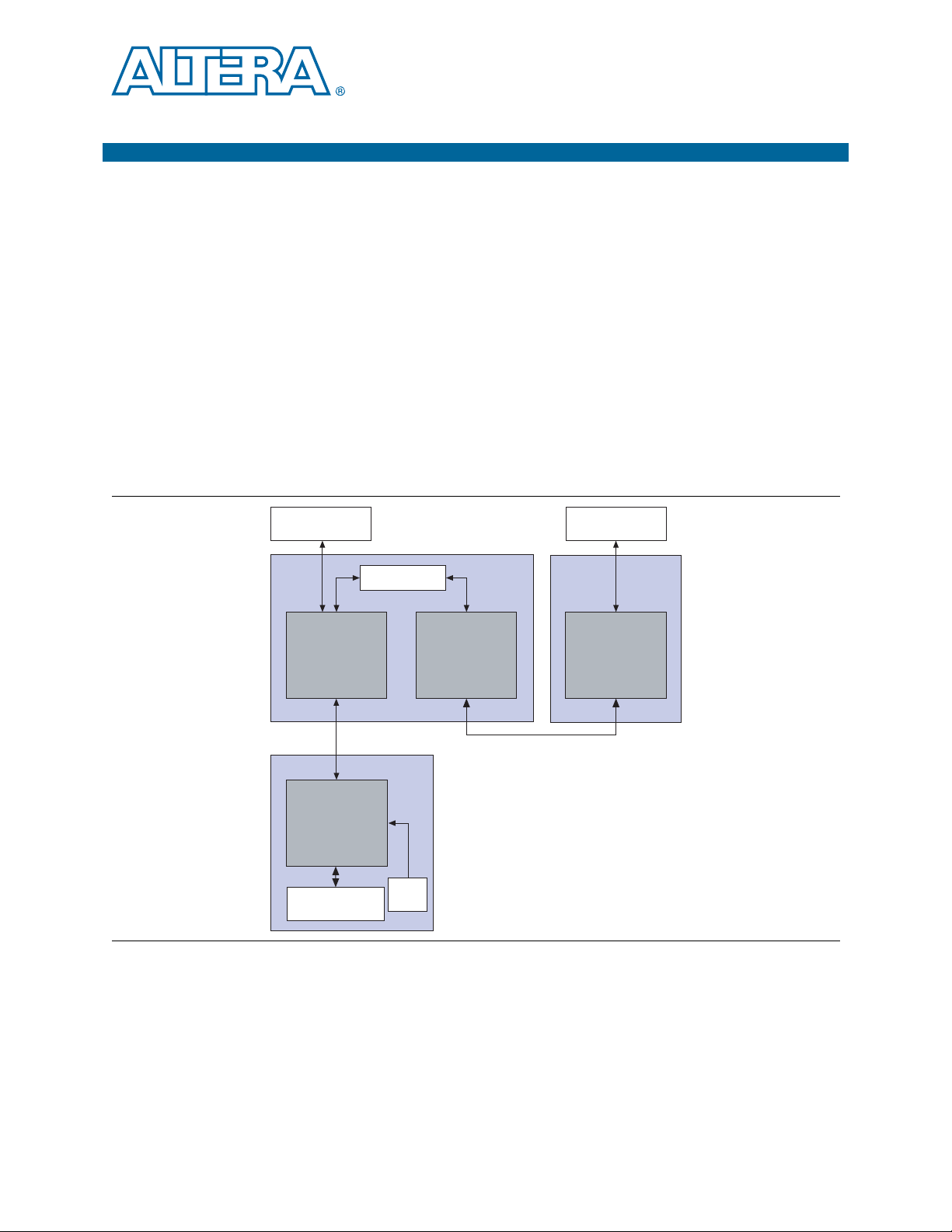
The Altera® CPRI MegaCore® function implements the Common Public Radio
CPRI
MegaCore Function
(RE Slave)
FPGA FPGA
CPRI
MegaCore Function
(RE Slave)
CPRI
MegaCore Function
(RE Master)
FPGA
CPRI
MegaCore Function
(REC)
Clock
Module
RF
Base Band Module
Optical Link
Optical Link
CPRICPRICPRI
CPRI
RF
Routing Layer
MAP MAPAUX AUX
Interface (CPRI) specification. CPRI is a high-speed serial interface designed for
network radio equipment controllers (REC) to receive data from and provide data to
remote radio equipment (RE).
1 The information in this user guide, including the latency numbers in “Delay
Measurement and Calibration Features” on page E–1, is applicable to version 13.1 of
the CPRI IP core.
The CPRI IP core targets high-performance, remote, radio network applications. You
can configure the CPRI IP core as an RE or an REC. Figure 1–1 shows an example
system implementation with a two-hop daisy chain. Optical links between devices
support high performance.
Figure 1–1. Typical CPRI Application on Altera Devices
1. About This MegaCore Function
December 2013 Altera Corporation CPRI MegaCore Function
User Guide
Page 8

1–2 Chapter 1: About This MegaCore Function
General Description
General Description
The Altera CPRI IP core implements Layer 1 and Layer 2 of the CPRI V5.0
specification. It provides access to the V5.0 Layer 1 and Layer 2 access points through
various interfaces:
■ V5.0 Layer 1 access:
■ Auxiliary (AUX) interface for full access to V5.0 control data stream for
antenna-carrier (Ctrl_AxC) bytes in control word.
■ Register support for loading and unloading full control words, including
Ctrl_AxC bytes.
■ Auxiliary (AUX) interface support for user-defined GSM mapping.
■ IQ data access:
■ Mapping block (MAP) to antenna-carrier interfaces for easy IQ user data plane
access based on pre-configured antenna-carrier channels.
■ Auxiliary (AUX) interface for full access to the user data plane.
■ Ethernet channel access:
■ Auxiliary interface for full access to the Ethernet space in the CPRI frame.
■ Register support for loading and unloading the Ethernet frame.
■ Media independent (MI) interface port for Ethernet Frame access.
■ High level data link control (HDLC) channel access:
■ Auxiliary interface for full access to the HDLC space in the CPRI frame.
■ Register support for loading and unloading the HDLC frame.
■ Vendor-specific space (VSS) data:
■ Auxiliary interface for full access to control words.
■ Register support for loading and unloading full control words, including VSS
space.
■ Synchronization and timing access:
■ Auxiliary interface for full access to synchronization and timing.
You configure the CPRI IP core to include an Ethernet media access control (MAC)
block or to communicate with an external Ethernet module through an MI interface.
You can configure the CPRI link line rate.
For information about the CPRI IP core interfaces and functionality, refer to Chapter 4,
Functional Description. For information about configuration options, refer to
Chapter 3, Parameter Settings.
CPRI MegaCore Function December 2013 Altera Corporation
User Guide
Page 9
Chapter 1: About This MegaCore Function 1–3
tx_dataout
Transmitter
Transceiver
Transmitter
rx_datain
CPRI LinkCPRI Link
Receiver
Transceiver
Receiver
Multiplexing
Time Division Multiplexing
IQ
Data
Full access
to
CPRI frame
Vendor
Specific
L1
Inband
Protocol
HDLC (2) Ethernet (3)
MAP
Interface (1)
AUX
Interface
CPU
Interface
MI
Interface
CPRI IP Core Features
Figure 1–2 shows the CPRI IP core interfaces. The IP core assembles the outbound
CPRI frame control words and data from all of these interfaces, and unloads and
routes control words and data from the inbound CPRI frame to the appropriate
interfaces, based on configuration and register settings.
Figure 1–2. CPRI IP Core Interfaces
Notes to Figure 1–2:
(1) You can configure your CPRI IP core with zero, one, or multiple antenna-carrier interfaces. If you configure zero antenna-carrier interfaces, the
MAP interface is not configured in your CPRI IP core. In that case you can communicate IQ data through the AUX interface to your user-defined
routing layer.
(2) You can configure your CPRI IP core with or without an HDLC block.
(3) You can configure your CPRI IP core with an Ethernet MAC block or a media-independent (MI) interface (MII) block. The two options are mutually
exclusive.
CPRI IP Core Features
The CPRI IP core has the following features:
■ Complies with the Common Public Radio Interface (CPRI) Specification V5.0
(2011-09-21) Interface Specification for wireless base station submodule
interconnections, without the full range of IQ data sample widths, using auxiliary
interface for user-defined GSM mapping.
■ Supports radio equipment controller (REC) and radio equipment (RE) module
configurations, including RE master, RE slave, and REC master ports.
■ Supports Universal Mobile Telecommunication System (UMTS) Terrestrial Radio
Access (UTRA) – frequency division duplexing (UTRA-FDD) (UMTS/Wideband
Code Division Multiple Access (W-CDMA)), Evolved UTRA (E-UTRA) (3rd
Generation Partnership Project (3GPP) Long Term Evolution (LTE) specification),
3GPP Global System for Mobile Communications (GSM)/Enhanced Data Rates for
GSM Evolution (EDGE) Radio Access Network, and Worldwide interoperability
■ Provides full access to CPRI frame.
for Microwave Access (WiMAX) (IEEE 802.16 standard).
December 2013 Altera Corporation CPRI MegaCore Function
User Guide
Page 10

1–4 Chapter 1: About This MegaCore Function
CPRI IP Core Features
■ Supports the following additional CPRI link features:
■ Programmable CPRI communication line rate (to 614.4, 1228.8, 2457.6, 3072.0,
4915.2, 6144.0, or 9830.4 Mbps) using Altera on-chip high-speed transceivers.
■ Programmable operation mode: CPRI link master or CPRI link slave.
■ Auto-rate negotiation support.
■ Scrambling and descrambling at 4915.2 Mbps, 6144.0 Mbps, and 9830.4 Mbps.
■ Receiver (Rx) delay measurement.
■ Transmitter (Tx) delay calibration.
■ Programmable hardware processing of the reset request bit in the CPRI frame.
■ Vendor-specific subchannel (VSS) communication on the CPRI link.
■ Diagnostic parallel reverse loopback paths.
■ Diagnostic stand-alone RE slave testing mode.
■ Includes the following additional interfaces:
■ Interface to external or on-chip processor, using the Altera Avalon
®
Memory-Mapped (Avalon-MM) interconnect specification.
■ Ethernet communication interfaces that support simultaneous Ethernet and
HDLC communication to and from the CPRI link.
■ Optional configuration of Ethernet MAC.
■ Optional Media-Independent Interface for Ethernet frame access.
■ Optional configuration of HDLC block.
■ Auxiliary interface provides full access to CPRI frame.
■ Supports data transfer to and from custom mapping functions, including
user-defined GSM mapping.
■ Supports data transfer from slave to master ports to implement daisy-chain
topologies.
■ Supports custom IQ sample widths.
■ Optional built-in IQ data interface with the following features:
■ Implements mapping methods in Sections 4.2.7.2.5 and 4.2.7.2.7 of the CPRI
V4.2 Specification, and mapping Options 1 and 2 in Sections 4.2.7.2.3 and
4.2.7.2.4 of the CPRI V4.2 Specification.
■ Implements WiMAX mapping methods described in Sections 4.2.7.2.2,
4.2.7.2.5, and 4.2.7.2.7 of the CPRI V4.2 Specification.
■ Implements UMTS/LTE mapping methods described in Section 4.2.7.2 of
the CPRI V4.2 Specification.
■ Implements WiMAX timing control methodology described in Section
4.2.8.2 of the CPRI V4.2 Specification.
■ Supports as many as 24 antenna-carrier interfaces.
■ Supports clocking antenna-carrier interfaces with external data channel
clocks or internal IP core clock.
CPRI MegaCore Function December 2013 Altera Corporation
User Guide
Page 11
Chapter 1: About This MegaCore Function 1–5
Device Family Support
■ Supports synchronous buffer or simple FIFO synchronization modes for
externally clocked antenna-carrier interfaces.
■ Supports independent sample rates for each antenna-carrier interface.
■ Supports 15- and 16-bit data sample widths on uplink and downlink using
the Altera Avalon Streaming (Avalon-ST) interconnect specification.
Device Family Support
Tab le 1– 1 defines the device support levels for Altera IP cores.
Table 1–1. Altera IP Core Device Support Levels
FPGA Device Families
Preliminary support—The IP core is verified with preliminary timing models for this device family.
The IP core meets all functional requirements, but might still be undergoing timing analysis for the
device family. It can be used in production designs with caution.
Final support—The IP core is verified with final timing models for this device family. The IP core
meets all functional and timing requirements for the device family and can be used in production
designs.
Tab le 1– 2 lists the level of support offered by the CPRI IP core for each Altera device
family.
Table 1–2. Device Family Support
Device Family Support
Stratix
®
V
Refer to the What’s New in Altera IP page of
the Altera website.
Stratix IV GX Final
®
V (GX, GT, and GZ variants) Preliminary
Arria
Arria II (GX and GZ variants) Final
®
Cyclone
V GX Preliminary
Cyclone IV GX Final
Other device families No support
Tab le 1– 3 shows the slowest device family speed grade that supports each CPRI line
rate in each device family. Lower speed grade numbers correspond to faster devices.
Table 1–3. Slowest Recommended Device Family Speed Grades
Device Family
or Variant
614.4 1228.8 2457.6 3072.0 4915.2 6144 9830.4
(1)
(Part 1 of 2)
CPRI Line Rate (Mbps)
Stratix V GX –4 –4 –4 –4 –4 –4 -2
StratixIVGX–4–4–4–4–4–3
Arria V GT C6 C6 C6 I5 I5 I5 I5
Arria V GX C6 C6 C6 I5 I5 I5
Arria V GZ –4 –4 –4 –4 –4 –4 –3
ArriaIIGX –6–6–6–6I3
(2)
(2) (3)
I3
(3)
(4)
(3)
December 2013 Altera Corporation CPRI MegaCore Function
User Guide
Page 12

1–6 Chapter 1: About This MegaCore Function
MegaCore Verification
Table 1–3. Slowest Recommended Device Family Speed Grades
Device Family
or Variant
614.4 1228.8 2457.6 3072.0 4915.2 6144 9830.4
ArriaIIGZ –4–4–4–4–3–3
CycloneVGXC8–7–7–7
Cyclone IV GX C8, I7 C8, I7 C8, I7 –7
Notes to Table 1–3:
(1) The entry –x indicates that both the industrial speed grade Ix and the commercial speed grade Cx are supported for this device family and CPRI
line rate.
(2) Only the I3 speed grade is available for a CPRI IP core that runs at this line rate and targets the Arria II GX device family.
(3) This CPRI line rate is not supported for this device family.
(4) Altera recommends that for designs that include a 9.8304 Gbps CPRI IP core variation that targets an Arria V GT device, you use multiple seeds
in the Quartus II Design Space Explorer to find the optimal Fitter settings to meet the timing constraints. Following the Timing Advisor's
recommendations, including optimizing for speed and using LogicLock regions may be necessary to meet timing, especially for more complex
variations implemented in the largest devices.
(1)
(Part 2 of 2)
CPRI Line Rate (Mbps)
(3)
(3) (3) (3)
(3) (3) (3)
MegaCore Verification
Before releasing a version of the CPRI IP core, Altera runs comprehensive regression
tests in the current version of the Quartus
MegaWizard
™
Plug-In Manager to create the instance files. Altera tests these files in
simulation and hardware to confirm functionality.
®
II software. These tests use the
Altera tests and verifies the CPRI IP core in hardware, especially the deterministic
latency feature, for different platforms and environments.
Performance and Resource Utilization
This section contains tables showing IP core variation size and performance examples.
For resource utilization information for additional CPRI IP core variations, refer to the
reports the Quartus II software generates during compilation.
Tab le 1– 4 lists the resources and expected performance for CPRI IP core variations
configured with the following features:
■ Operate in REC master mode
■ Include autorate negotiation support
■ Provide Ethernet access through the MI interface
■ Do not provide an HDLC block
■ Use Basic mapping mode
■ Clock the AxC channels with independent clocks (the Enable MAP interface
synchronization with core clock parameter is turned off)
■ Do not include automatic round-trip delay calibration logic
■ Do not include VSS access through the CPU interface
The numbers of ALMs and logic registers are rounded up to the nearest 100.
CPRI MegaCore Function December 2013 Altera Corporation
User Guide
Page 13

Chapter 1: About This MegaCore Function 1–7
Performance and Resource Utilization
Tab le 1– 4 lists results obtained with the Quartus II software v12.1 SP1 for the
following devices:
■ Stratix V GX (5SGXMA5N3F40I4
■ Arria V GT (5AGTMD3G3F31I3)
■ Arria V GX (5AGXFB3H6F35C6 for 614.4, 1228.8, 2457.6, and 3072 Mbps variations
and 5AGXFB3H4F35I5 for other variations)
■ Arria V GZ (5AGZME7K3F40I4)
■ Cyclone V GX (5CGXFC9E7F35C8 for 6144 Mbps variations and 5CGXFC9E6F35I7
for 122.8, 2457.6, and 3072 Mbps variations)
Table 1–4. CPRI IP Core FPGA Resource Utilization (Part 1 of 2)
Device
Stratix V GX
Arria GZ
Line Rate
(Mbps)
614.4
1228.8,
2457.6,
3072.0,
4915.2
6144.0,
9830.4
614.4
1228.8,
2457.6,
3072.0,
4915.2
6144.0,
9830.4
Number of
Antenna-Carrier
Interfaces
ALMs
Primary
Register
Secondary
Register
0 2089 2346 230 3
1 2695 3218 323 9
2 2867 3499 330 11
3 3032 3703 343 13
4 3185 3943 394 15
0 2062 2331 217 3
1 2662 3128 317 9
4 3126 3770 333 15
8 3810 4582 410 23
0 2450 3408 350 3
1 3241 4990 546 9
4 3734 5687 606 15
8 4443 6581 697 23
0 2068 2356 230 3
1 2786 3368 299 9
2 2984 3589 352 11
3 3189 3818 403 13
4 3378 4073 285 15
0 2029 2319 221 3
1 2796 3309 210 9
4 3321 3891 371 15
8 3998 4737 428 23
0 2438 3451 219 3
1 3488 5145 515 9
4 3988 5844 649 15
8 4651 6806 707 23
M10K or M20K
Blocks
(1)
December 2013 Altera Corporation CPRI MegaCore Function
User Guide
Page 14

1–8 Chapter 1: About This MegaCore Function
Release Information
Table 1–4. CPRI IP Core FPGA Resource Utilization (Part 2 of 2)
Number of
Antenna-Carrier
Interfaces
ALMs
Primary
Register
Secondary
Register
Device
Line Rate
(Mbps)
0 6649 9239 738 5
Arria V GT
(Soft PCS
Variant)
9830.4
1 7523 10979 911 15
4 7990 11718 922 21
8 8696 12707 1057 29
0 2299 2321 202 3
1 2983 3131 428 15
614.4
2 3117 3332 291 17
3 3324 3553 287 19
4 3560 3795 414 21
0 2266 2345 175 3
Arria V GX
1228.8,
2457.6,
3072.0
1 2924 3157 186 15
4 3484 3811 237 21
8 4126 4635 285 29
0 3254 5156 169 3
4915.2,
6144.0
1 4065 6702 421 13
4 4568 7473 411 19
8 5689 8402 425 27
0 2398 2416 410 3
1 3200 3526 580 14
614.4
2 3401 3667 648 16
3 3580 3931 609 18
Cyclone V
4 3667 4016 594 20
0 2238 2417 133 3
1228.8,
2457.6,
3072.0
1 3139 3494 170 14
4 3704 4006 247 20
8 4501 4842 302 28
Note to Table 1–4:
(1) M10K blocks in Arria V GX, Arria V GT, and Cyclone V GX devices and M20K blocks in Arria V GZ and Stratix V devices.
M10K or M20K
Blocks
(1)
Release Information
Tab le 1– 5 provides information about this release of the CPRI IP core.
Table 1–5. CPRI Release Information (Part 1 of 2)
Item Description
Version 13.1
Release Date November 2013
Ordering Code IP-CPRI
CPRI MegaCore Function December 2013 Altera Corporation
User Guide
Page 15
Chapter 1: About This MegaCore Function 1–9
Installation and Licensing
Table 1–5. CPRI Release Information (Part 2 of 2)
Item Description
Product ID 00CB
Vendor ID 6AF7
Altera verifies that the current version of the Quartus II software compiles the
previous version of each Altera IP core. Any exceptions to this verification are
reported in the MegaCore IP Library Release Notes and Errata. Altera does not verify
compilation with IP core versions older than the previous release.
Installation and Licensing
The CPRI IP core is part of the MegaCore IP Library, which is distributed with the
Quartus II software. The combined software is downloadable from the Altera website,
www.altera.com.
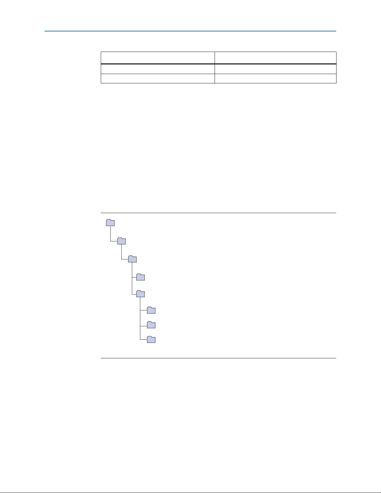
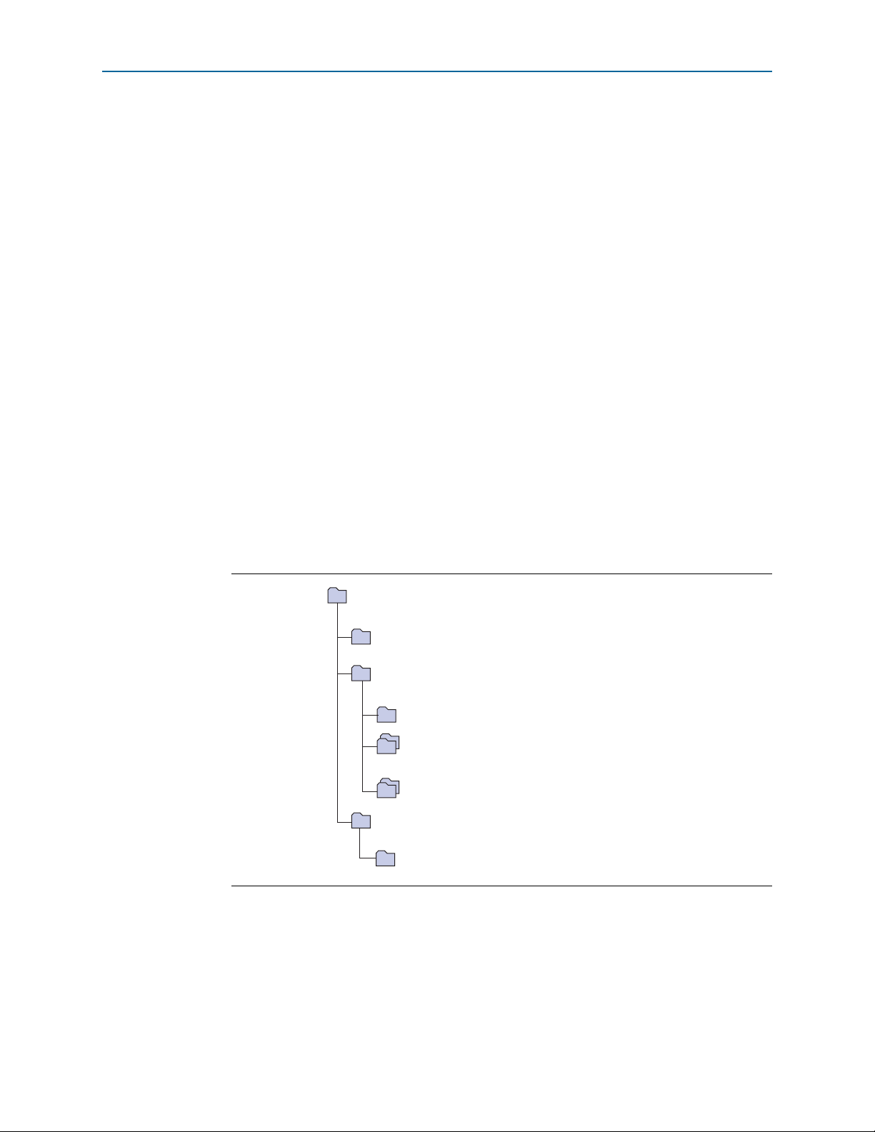
Figure 1–3 shows the directory structure after you install the CPRI IP core, where
<
path> is the installation directory. The default installation directory on Windows is
C:\altera\<version number>; on Linux it is /opt/altera<version number>.
Figure 1–3. Directory Structure
<path>
Installation directory
ip
Contains the Altera MegaCore IP Library and third-party IP cores
altera
Contains the Altera MegaCore IP Library
common
Contains shared components
cpri
Contains the CPRI IP core files
src
Contains the CPRI IP core encrypted lower-level design files
constraints
Contains the Synopsys Design Constraints and Tcl constraints scripts for the CPRI IP core
cus_demo_tb
Contains the demonstration testbenches for the CPRI IP core
You can use Altera’s free OpenCore Plus evaluation feature to evaluate the CPRI IP
core in simulation and in hardware before you purchase a license. You must purchase
a license for the CPRI IP core only when you are satisfied with its functionality and
performance, and you want to take your design to production.
After you purchase a license for the CPRI IP core, you can request a license file from
the Altera website at www.altera.com/licensing and install it on your computer.
When you request a license file, Altera emails you a license.dat file. If you do not have
internet access, contact your local Altera representative.
December 2013 Altera Corporation CPRI MegaCore Function
User Guide
Page 16

1–10 Chapter 1: About This MegaCore Function
Installation and Licensing
OpenCore Plus Evaluation
With the Altera free OpenCore Plus evaluation feature, you can perform the following
actions:
■ Simulate the behavior of a megafunction (Altera IP core or AMPP
SM
megafunction) in your system using the Quartus II software and Altera-supported
VHDL and Verilog HDL simulators
■ Verify the functionality of your design and evaluate its size and speed quickly and
easily
■ Generate time-limited device programming files for designs that include Altera IP
cores
■ Program a device and verify your design in hardware
OpenCore Plus Time-Out Behavior
OpenCore Plus hardware evaluation supports the following two operation modes:
■ Untethered—the design runs for a limited time.
■ Tethered—requires a connection between your board and the host computer. If
tethered mode is supported by all megafunctions in a design, the device can
operate for a longer time or indefinitely.
All megafunctions in a device time out simultaneously when the most restrictive
evaluation time is reached. If there is more than one megafunction in a design, a
specific megafunction's time-out behavior might be masked by the time-out behavior
of the other megafunctions.
1 For Altera IP cores, the untethered time-out is 1 hour; the tethered time-out value is
indefinite.
Your design stops working after the hardware evaluation time expires.
The CPRI IP core then behaves as if the
reset
and
cpu_reset
signals are asserted: the
CPRI link and the CPU interface reset. The transceivers do not reset, because the
transceiver quad might be shared with other designs, IP cores, and megafunctions.
The CPRI IP core cannot achieve frame synchronization, and cannot participate in
further CPRI communication.
f For information about installation and licensing, refer to Altera Software Installation and
Licensing. For information about the OpenCore Plus evaluation feature, refer to
AN 320: OpenCore Plus Evaluation of Megafunctions.
CPRI MegaCore Function December 2013 Altera Corporation
User Guide
Page 17
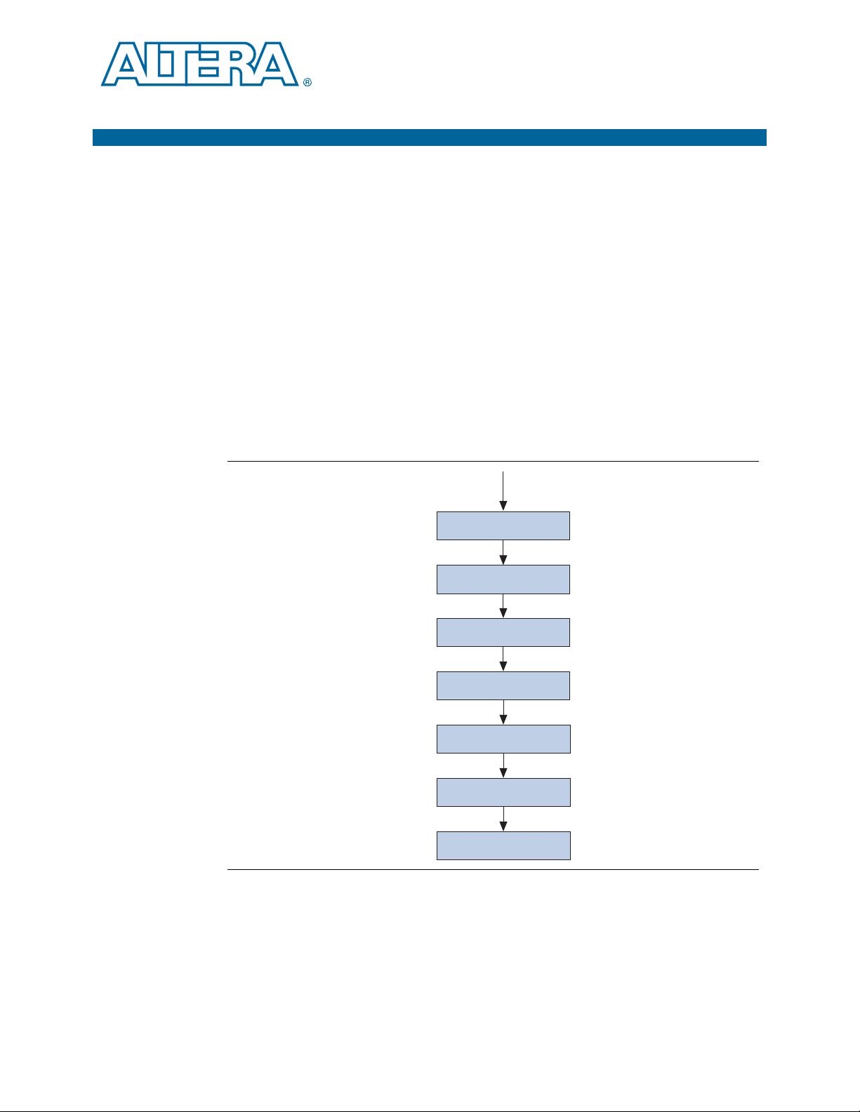
You can customize the CPRI IP core to support a wide variety of applications. You use
MegaWizard Plug-In
Manager Flow
Instantiate MegaCore
In Design
Specify Constraints
Specify Parameters
Generate
MegaCore Function
Compile Design
Program Device
Simulate with
T estbench
Generate
MegaCore Function
the MegaWizard Plug-In Manager in the Quartus II software to parameterize a
custom IP core variation in a CPRI parameter editor. The CPRI parameter editor lets
you interactively set parameter values and select optional ports.
The CPRI IP core supports the Altera MegaWizard Plug-In Manager design flow. The
CPRI IP core is not available in the Qsys design flow. To include a CPRI IP core in your
Qsys-based design, you must generate the IP core in the MegaWizard Plug-In
Manager design flow and connect it manually in the design.
MegaWizard Plug-In Manager Design Flow
Figure 2–1 shows the stages for creating a system with the CPRI IP core and the
Quartus II software. Each stage is described in detail in subsequent sections.
Figure 2–1. CPRI Design Flow
2. Getting Started
The MegaWizard Plug-In Manager flow allows you to customize the CPRI IP core,
and manually integrate the function in your design.
December 2013 Altera Corporation CPRI MegaCore Function
User Guide
Page 18

2–2 Chapter 2: Getting Started
MegaWizard Plug-In Manager Design Flow
Specifying Parameters
To specify CPRI IP core parameters using the MegaWizard Plug-In Manager, perform
the following steps:
1. Create a Quartus II project using the New Project Wizard available from the File
menu.
2. Launch the MegaWizard Plug-In Manager from the Tools menu, and follow the
prompts in the MegaWizard Plug-In Manager interface to create a custom CPRI IP
core variation.
To select the CPRI IP core, click
Installed Plug-Ins > Interfaces > CPRI > CPRI v13.1.
3. Specify the parameters. For details about these parameters, refer to Chapter 3,
Parameter Settings.
As you specify parameters, the CPRI parameter editor displays messages about
the variation that your current settings define.
If your settings define a variation for which an autorate negotiation testbench can
be automatically generated when the CPRI IP core is generated, an information
message tells you the name of the relevant autorate negotiation testbench. For
more information about the autorate negotiation testbench and the variations that
provide it, refer to Appendix C, CPRI Autorate Negotiation Testbench.
For information about the other testbenches that can be automatically generated
with the CPRI IP core, but for which no information messages appear, refer to
Chapter 8, CPRI IP Core Demonstration Testbench.
4. Click Finish to generate the CPRI IP core and supporting files.
You might have to wait several minutes for file generation to complete.
5. When you are prompted to generate an example design, turn on Generate
Example Design. You must turn on this option to generate the testbenches
described in Chapter 8, CPRI IP Core Demonstration Testbench and in
Appendix C, CPRI Autorate Negotiation Testbench.
The prompt appears even for those few CPRI IP core variations for which no
testbench is generated. If you are generating a variation for which no testbench is
available, and you turn on Generate Example Design, a directory with
compile.tcl files is generated. You can use these compile.tcl files as initial
templates to build your own testbench.
6. Click Generate. Despite the moving progress bar, generation does not progress
until you click this button.
7. If you generate the CPRI IP core instance in a Quartus II project, you are prompted
to add the Quartus II IP File (.qip) to the current Quartus II project. You can also
turn on Automatically add Quartus II IP Files to all projects.
The .qip file is generated by the parameter editor, and contains information about
the generated IP core. In most cases, the .qip file contains all of the necessary
information required to process the IP core in the Quartus II compiler. The
parameter editor generates a single .qip file for each instance of the IP core.
CPRI MegaCore Function December 2013 Altera Corporation
User Guide
Page 19
Chapter 2: Getting Started 2–3
MegaWizard Plug-In Manager Design Flow
Generating your custom CPRI IP core variation creates a set of HDL files and
simulation models. You can now integrate your custom CPRI IP core variation in your
design, simulate, and compile.
Simulation Files
Generating a CPRI IP core creates an <instance_name>_sim directory with a
subdirectory for each of four different Altera-supported simulators for the current
software release. Each of the vendor-specific directories contains files and scripts to
simulate your CPRI IP core with that vendor’s simulation tools.
The <instance_name>_sim/altera_cpri directory contains the top-level simulation file
for your CPRI IP core.
Generating a CPRI IP core creates a more complex directory structure for Arria V,
Cyclone V, and Stratix V variations than for variations that target other device
families, because the Arria V, Cyclone V, and Stratix V variations instantiate an Altera
Deterministic Latency PHY IP core or an Altera Native PHY IP core. In an Arria V,
Cyclone V, or Stratix V variation, your <instance_name>_sim directory contains
multiple subdirectories, one for each of the various components in the CPRI IP core, in
addition to the individual directories for vendors for four different simulators.
Figure 2–2 shows the directory structure of your CPRI IP core that contains a
Deterministic Latency PHY IP core and generates a testbench. Not all CPRI IP core
variations provide matching demonstration testbenches. For information about the
CPRI IP core variations that provide a testbench, refer to “Simulating the Design”.
Figure 2–2. Generated CPRI IP Core Directory Structure for Most 28-nm Variations
<working directory>
Quartus II project working directory
<instance name>
CPRI IP core instance HDL files
<instance name>_sim
CPRI IP core instance simulation files and scripts
altera_cpri
Contains the CPRI IP core instance top-level simulation file
altera_cpri_instance, altera_merlin_master_translator,
altera_merlin_slave_translator, altera_xcvr_det_latency
Contain the CPRI IP core instance lower-level simulation files
Vendor-specific directories contain simulation scripts
<instance name>_testbench
Contains the VHDL and System Verilog testbench simulation files
altera_cpri
Contains the lower-level testbench simulation files
The altera_xcvr_det_latency directory contains the files to simulate the Altera
Deterministic Latency PHY IP core that is generated as part of your CPRI IP core. It
also contains a mentor subdirectory with IEEE encrypted files to simulate the PHY IP
core efficiently.
December 2013 Altera Corporation CPRI MegaCore Function
User Guide
Page 20

2–4 Chapter 2: Getting Started
MegaWizard Plug-In Manager Design Flow
Simulating the Design
During the design process, to check your design quickly, you can simulate your CPRI
IP core with any of several Altera-supported EDA simulation tools.
f For more information about these tools and how to simulate designs created using the
Quartus II software, refer to the “Simulation” section in volume 3 of the Quartus II
Handbook.
Most CPRI IP core variations support a demonstration testbench. You can simulate
your CPRI IP core variation using its IP functional simulation model and
demonstration testbench. The IP functional simulation model, and testbench files for
the CPRI IP core variations that support demonstration testbenches, are generated in
your project directory when you generate your CPRI IP core. The testbench files
include scripts to compile and run the demonstration testbench. The testbench
demonstrates how to instantiate a model in a design and includes simple stimuli to
control the user interfaces of the CPRI IP core.
1 The autorate negotiation testbench is generated in VHDL, and the non-autorate
negotiation testbench is generated in System Verilog. If you specify Verilog HDL in
the MegaWizard Plug-In Manager, it generates a Verilog HDL IP functional
simulation model for the CPRI IP core. If you specify VHDL, the MegaWizard Plug-In
Manager generates a VHDL IP functional simulation model for the CPRI IP core.
Testbenches are generated as supported by the CPRI IP core variation you specify if
you turn on Generate Example Design. You can use the Verilog HDL functional
simulation model with the VHDL demonstration testbench for simulation, or vice
versa, using a mixed-language simulator.
For a complete list of models or libraries required to simulate the CPRI IP core, refer to
the compile.tcl scripts provided with the demonstration testbenches described in
Chapter 8, CPRI IP Core Demonstration Testbench and in Appendix C, CPRI Autorate
Negotiation Testbench. If you turn on Generate Example Design for a variation
without a demonstration testbench, you can view the example scripts in the generated
testbench directory, and use them as a basis to assist you in building your own
testbench.
Not all variations provide demonstration testbenches. To run a demonstration
testbench, you must generate a variation that provides a working testbench. To ensure
your CPRI variation has a non-autorate negotiation testbench you can simulate, set
the following values in the CPRI parameter editor:
■ Operation mode must have the value of Master.
■ If the CPRI variation has a MAP interface, Mapping mode must have the value of
All or Basic.
■ If the CPRI variation has a MAP interface, Enable MAP interface synchronization
with core clock must be turned off.
To ensure your CPRI variation has an autorate negotiation testbench, set the following
values in the CPRI parameter editor:
■ Operation mode must have the value of Master.
■ Enable auto-rate negotiation must be turned on.
CPRI MegaCore Function December 2013 Altera Corporation
User Guide
Page 21

Chapter 2: Getting Started 2–5
Integrating the CPRI IP Core in a Design
■ Include MAC block must be turned on.
■ Number of antenna-carrier interfaces must have the value of zero.
■ Include HDLC block must be turned off.
Refer to Chapter 3, Parameter Settings for information about these parameter values.
Refer to Chapter 8, CPRI IP Core Demonstration Testbench for more information
about the non-autorate negotiation testbench and to Appendix C, CPRI Autorate
Negotiation Testbench for more information about the autorate negotiation testbench.
f For information about IP functional simulation models, refer to the Simulating Altera
Designs chapter in volume 3 of the Quartus II Handbook.
Integrating the CPRI IP Core in a Design
To compile the CPRI IP core and configure it on a device, you must integrate it in a
Quartus II project that provides additional functionality and constraints.
Supporting the Transceivers
When you integrate your CPRI IP core variation in your design, observe the following
connection requirements:
■ In Arria II, Cyclone IV GX, and Stratix IV GX designs:
■ Ensure that you connect the calibration clock (
signal with the appropriate frequency range of 10–125 MHz. The
gxb_cal_blk_clk
) to a clock
cal_blk_clk
ports on other components that use transceivers must be connected to the same
clock signal.
■ Add a dynamic reconfiguration block (
altgx_reconfig
) and connect it as
specified in the Arria II Device Handbook, Cyclone IV Device Handbook, or
Stratix IV Device Handbook. This block supports offset cancellation to
compensate for analog voltages offset from required ranges due to process
variations. This block is not required for CPRI IP core autorate negotiation to
function correctly. The design compiles without the
altgx_reconfig
block, but
it cannot function correctly in hardware.
■ In Arria V, Cyclone V, and Stratix V designs, add an Altera Transceiver
Reconfiguration Controller and connect it as specified in the Altera Transceiver PHY
IP Core User Guide. This block supports offset cancellation to compensate for
analog voltages offset from required ranges due to process variations. The design
does compile without the Altera Transceiver Reconfiguration Controller, with a
critical warning, but it cannot function correctly in hardware.
Specifying Constraints
Altera provides a Synopsys Design Constraints (.sdc) file that you must apply to
ensure that the CPRI IP core meets design timing requirements. In most cases the
script requires modification for your design. For modification guidelines, refer to
Appendix F, Integrating the CPRI IP Core Timing Constraints in the Full Design.
December 2013 Altera Corporation CPRI MegaCore Function
User Guide
Page 22

2–6 Chapter 2: Getting Started
In addition, before you compile your system to generate an SRAM Object File (.sof)
with which to configure your device, Altera recommends that you create assignments
for the high-speed transceiver VCCH settings.
To create assignments for the high-speed transceiver VCCH settings, perform the
following steps:
1. In the Quartus II window, on the Assignments menu, click Assignment Editor.
2. In the <<new>> cell in the To column, type the top-level signal name for your
CPRI IP core instance
3. Double-click in the Assignment Name column and click I/O Standard.
4. Double-click in the Val u e column and click your standard (for example, 1.5-V
PCML).
5. In the new <<new>> row, repeat steps 2 to 4 for your CPRI IP core instance
gxb_rxdatain
f For information about timing analyzers, refer to the Quartus II Help and the “Timing
Analysis” section in volume 3 of the Quartus II Handbook.
signal.
gxb_txdataout
signal.
Compiling and Programming the Device
Compiling and Programming the Device
You can use the Start Compilation command on the Processing menu in the
Quartus II software to compile your design. After successfully compiling your design,
program the targeted Altera device with the Programmer and verify the design in
hardware.
1 Before compiling your CPRI IP core or other incomplete CPRI design in the Quartus II
software, you must assign unconnected CPRI IP core signals to virtual pins.
f For information about compiling your design in the Quartus II software, refer to the
Quartus II Incremental Compilation for Hierarchical and Team-Based Design chapter in
volume 1 of the Quartus II Handbook. For information about programming an Altera
device, refer to the “Device Programming” section in volume 3 of the Quartus II
Handbook.
Instantiating Multiple CPRI IP Cores
If you want to instantiate multiple CPRI IP cores in an Arria II, Cyclone IV GX, or
Stratix IV GX device, to ensure your design optimizes its use of device pins, you must
observe the following additional requirements:
CPRI MegaCore Function December 2013 Altera Corporation
User Guide
Page 23

Chapter 2: Getting Started 2–7
Instantiating Multiple CPRI IP Cores
■ You m u st en su re t ha t th e
gxb_cal_blk_clk
input and
gxb_powerdown
signals are
connected according to the requirements for your target device family.
■ You must ensure that a single calibration clock source drives the
gxb_cal_blk_clk
input to each CPRI IP core (or any other megafunction or
user logic that uses the ALTGX megafunction).
■ When you merge multiple CPRI IP cores in a single transceiver block, the same
signal must drive
gxb_powerdown
to each of the CPRI IP core variations and
other megafunctions, Altera IP cores, and user logic that use the ALTGX
megafunction.
■ You must ensure that the instances each have different starting channel numbers.
Multiple CPRI IP cores in a single device must use distinct transceiver channels.
You enforce this restriction by specifying different starting channel numbers for
the distinct CPRI IP cores. Refer to Chapter 3, Parameter Settings.
■ To configure multiple CPRI IP cores in a single transceiver block, you must specify
in your Quartus Settings File (.qsf) that these CPRI link data lines are configured
in the same
outgoing CPRI link
set_instance_assignment -name GXB_TX_PLL_RECONFIG_GROUP 1 -to cN_gxb_txdataout
GXB_TX_PLL_RECONFIG_GROUP
cN_gxb_txdataout
:
, using the following syntax for each
December 2013 Altera Corporation CPRI MegaCore Function
User Guide
Page 24

2–8 Chapter 2: Getting Started
Instantiating Multiple CPRI IP Cores
CPRI MegaCore Function December 2013 Altera Corporation
User Guide
Page 25

3. Parameter Settings
You customize the CPRI IP core by specifying parameters in the CPRI parameter
editor, which you access from the MegaWizard Plug-In Manager in the Quartus II
software.
This chapter describes the parameters and how they affect the behavior of the CPRI IP
core. You can modify parameter values to specify the following CPRI IP core
properties:
■ Default clocking mode—whether this CPRI IP core instance is configured initially
with slave clocking mode (RE slave) or with master clocking mode (REC or RE
master).
■ Line rate.
■ Autorate negotiation—whether this CPRI IP core instance supports the connection
of external logic to implement autorate negotiation.
■ Starting channel number. This option is available only in the following devices:
■ Arria II GX and Arria II GZ
■ Cyclone IV
■ Stratix IV
■ Depth of the low-level receiver elastic buffer.
■ Transceiver reference clock frequency. This option is available only in Arria V,
Cyclone V, and Stratix V devices.
■ Ethernet MAC—whether to include an internal Ethernet MAC block or provide an
MII to connect to an external Ethernet module. These two options are mutually
exclusive.
■ HDLC block—whether to include an internal HDLC block or not.
■ Number of antenna-carrier interfaces.
■ Whether the antenna-carrier interfaces are clocked by the CPRI IP core clock
cpri_clkout
■ Mapping modes—select the mode: All, Basic, Advanced1, Advanced2, and
or by external clocks.
Advanced3.
■ Whether to include an automatic round-trip delay calibration block or not.
■ Whether to allow vendor-specific space (VSS) access through the CPU interface or
not.
Physical Layer Parameters
This section lists the parameters that affect the configuration of the physical layer of
the CPRI IP core.
December 2013 Altera Corporation CPRI MegaCore Function
User Guide
Page 26

3–2 Chapter 3: Parameter Settings
Physical Layer Parameters
Operation Mode Parameter
The Operation mode parameter specifies whether the CPRI IP core is configured with
slave clocking mode or with master clocking mode. An REC is configured with master
clocking mode.
The value of this parameter determines the initial operation mode of the CPRI IP core.
In IP core variations that target an Arria V, Cyclone V, or Stratix V device, you can
modify the IP core operation mode dynamically by modifying the value of the
operation_mode
bit of the
CPRI_CONFIG
register (Table 7–6 on page 7–4).
In your design, you must connect the clocks appropriately for the operation mode.
Refer to “Clock Diagrams for the CPRI IP Core” on page 4–5.
For information about how to dynamically switch the clock mode of your CPRI IP
core in variations that target an Arria V, Cyclone V, or Stratix V device, refer to
“Dynamically Switching Clock Mode” on page 4–9.
Line Rate Parameter
The Line rate parameter specifies the line rate on the CPRI link in gigabits per second
(Gbps). Ta bl e 3 –1 lists the CPRI line rates that each device family supports. A
checkmark indicates a supported variation.
Table 3–1. Device Family Support for CPRI Line Rates
Device Family
or Variant
Arria II GX vvvvvv—
Arria II GZ vvvvvv—
Arria V GX vvvvvv—
Arria V GT vvvvvvv
Arria V GZ vvvvvvv
Cyclone IV GX vvvv———
Cyclone V GX vvvv———
Stratix IV GX vvvvvv—
Stratix V GX vvvvvvv
Stratix V GT vvvvvvv
Note to Tab le 3– 1:
(1) Refer to Table 1–3 on page 1–5 for information about the device speed grades that support each CPRI line rate.
The parameter editor does not enforce these restrictions. However, if you target a device whose speed grade does
not support the CPRI line rate you configure, compilation fails because the design cannot meet timing in hardware.
0.6144 1.2288 2.4576 3.072 4.9152 6.144 9.8304
CPRI Line Rate (Gbps)
(1)
CPRI MegaCore Function December 2013 Altera Corporation
User Guide
Page 27

Chapter 3: Parameter Settings 3–3
Physical Layer Parameters
Enable Autorate Negotiation
Autorate negotiation is the process of stepping down from a higher target CPRI line
rate to a lower target CPRI line rate if you are unable to establish a link at the higher
line rate. If your CPRI IP core has autorate negotiation enabled, and you program it to
step down from its highest target CPRI line rate to its lower target CPRI line rates
when it does not achieve frame synchronization, your CPRI IP core achieves frame
synchronization at the highest possible CPRI line rate in its range of potential line
rates, depending on the capability of its CPRI partner.
For information about the autorate negotiation feature, refer to Appendix B,
Implementing CPRI Link Autorate Negotiation.
Turn o n t he Enable auto-rate negotiation parameter to specify that your CPRI IP core
supports autorate negotiation. By default, this parameter is turned off.
Transceiver Starting Channel Number
You can specify the starting number for the CPRI IP core transceiver. For a CPRI IP
core master, the Master transceiver starting channel number specifies the starting
channel number for the transceiver.
For a CPRI IP core configured with slave clocking mode, the Slave transmitter
starting channel number and Slave receiver starting channel number are two
separate parameters. Both must have values that are starting channel numbers
available in your design. The two numbers must be different but the Quartus II
software creates an FPGA configuration with a single slave transceiver.
If you instantiate multiple CPRI IP cores on the same device, you must ensure each
uses distinct transceiver channels.
These parameters are not available in Arria V, Cyclone V, and Stratix V devices.
Rx Elastic Buffer Depth
You can specify the depth of the Rx elastic buffer in the CPRI Receiver block. The
Receiver buffer depth value is the log
are 4 to 8, inclusive.
The default depth of the Rx elastic buffer is 64, specified by the Receiver buffer depth
parameter default value of 6. For most systems, the default Rx elastic buffer depth is
adequate to handle dispersion, jitter, and drift that can occur on the link while the
system is running. However, the parameter is available for cases in which additional
depth is required.
1 Altera recommends that you set Receiver buffer depth to 4 in CPRI RE slave
variations.
of the Rx elastic buffer depth. Allowed values
2
CPRI IP core variations configured at a CPRI line rate of 9830.4 Mbps that target an
Arria V GT device do not include an Rx elastic buffer. However, this parameter affects
the depth of the RX buffer between the soft PCS and the Altera Transceiver Native
PHY IP core, instead. Refer to Figure 4–4 on page 4–8 and Figure 4–5 on page 4–9.
f For information about the Altera Transceiver Native PHY IP core, refer to the Altera
Transceiver PHY IP Core User Guide.
December 2013 Altera Corporation CPRI MegaCore Function
User Guide
Page 28

3–4 Chapter 3: Parameter Settings
The value you specify for Receiver buffer depth is referred to as WIDTH_RX_BUF in
this user guide.
For more information about the Rx elastic buffer, refer to “Rx Elastic Buffer” on
page 4–54.
Data Link Layer Parameters
Transceiver Reference Clock Frequency
If your CPRI variation targets an Arria V, Cyclone V, or Stratix V device, the
Transceiver reference clock frequency parameter is available. Use this parameter to
modify the expected frequency of the CPRI transceiver input reference clock to the
frequency of an available clock for your design.
The frequency you specify is an input parameter to the Altera Deterministic Latency
PHY IP core that is included in your Arria V, Cyclone V, or Stratix V CPRI variation.
Values available at each CPRI line rate are the reference clock frequencies for which
the Deterministic Latency PHY IP core supports the target CPRI line rate. The default
value is 122.88 MHz.
In the case of an Arria V GT variation configured with CPRI line rate 9830.4 Mbps, the
frequency is an input parameter to the Altera Native PHY IP core.
f For more information about the Altera Deterministic Latency PHY IP core and the
Altera Native PHY IP core, refer to the Altera Transceiver PHY IP Core User Guide.
Automatic Round-Trip Delay Calibration
Turn o n t he Automatic round-trip delay calibration parameter to specify that your
CPRI IP core includes the calibration logic. By default, the parameter is turned off.
f For more information on automatic round-trip calibration delay feature, refer to
“Dynamic Pipelining for Automatic Round-Trip Delay Calibration” on page E–19
Data Link Layer Parameters
This section lists the parameter that affects the configuration of the data link layer of
the CPRI IP core.
Include MAC Block
Turn o n t he Include MAC block parameter to specify that your CPRI IP core includes
an internal Ethernet MAC block. By default, this parameter is turned off. If this
parameter is turned off, the CPRI IP core implements the media-independent
interface (MII) to your own external Ethernet MAC, instead.
If this parameter is turned off in your CPRI IP core, your application cannot access the
Ethernet registers. Attempts to access these registers read zeroes and do not write
successfully, as for a reserved register address.
For information about the internal Ethernet MAC block, refer to “Accessing the
Ethernet Channel” on page 4–47.
For information about the MII, refer to “Media Independent Interface to an External
Ethernet Block” on page 4–37.
CPRI MegaCore Function December 2013 Altera Corporation
User Guide
Page 29

Chapter 3: Parameter Settings 3–5
Application Layer Parameters
Include HDLC Block
Turn o n t he Include HDLC block parameter to specify that your CPRI IP core
includes an internal HDLC block. By default, this parameter is turned off.
If this parameter is turned off in your CPRI IP core, your application cannot access the
HDLC registers. Attempts to access these registers read zeroes and do not write
successfully, as for a reserved register address.
For information about the HDLC block, refer to “Accessing the HDLC Channel” on
page 4–50.
Application Layer Parameters
This section lists the parameters that affect the configuration of the application layer
of the CPRI IP core.
Mapping Mode
The Mapping mode(s) parameter specifies whether your CPRI IP core MAP interface
supports a programmable AxC mapping mode or is configured with a specific
mapping mode. Tab le 3– 2 lists the supported values.
Table 3–2. MAP Interface AxC Mapping Mode Support (Part 1 of 2)
Value Description
If you select this value, you configure a CPRI IP core which you can program
dynamically to be in any mapping mode. In this case, you determine the current
mapping mode for your CPRI IP core by programming the
All
Basic
Advanced 1
CPRI_MAP_CONFIG
For backward compatibility with previous releases of the CPRI IP core, the value of
All is the default value for this parameter.
For information about the
page 7–15.
Your CPRI IP core MAP interface is configured to function in basic mapping mode
only. This mapping mode has the following features:
■ Conforms to the description in Sections 4.2.7.2.2 and 4.2.7.2.3 of the CPRI
Specification V4.2 Interface Specification.
■ Supports communication that complies with the LTE/E-UTRA or UMTS/WCDMA
standard.
For information about the basic mapping mode in the CPRI IP core, refer to “MAP
Interface Mapping Modes” on page 4–13.
Your CPRI IP core MAP interface is configured in a single AxC mapping mode only,
a mode that has the following features:
■ Conforms to Method 1: IQ Sample Based described in Section 4.2.7.2.5 of the
CPRI Specification V4.2 Interface Specification.
■ Supports communication that complies with the WiMAX standard.
For information about this AxC mapping mode, refer to Appendix D, Advanced AxC
Mapping Modes.
register (0x100).
map_mode
register field, refer to Table 7–31 on
map_mode
field of the
December 2013 Altera Corporation CPRI MegaCore Function
User Guide
Page 30

3–6 Chapter 3: Parameter Settings
Application Layer Parameters
Table 3–2. MAP Interface AxC Mapping Mode Support (Part 2 of 2)
Value Description
Your CPRI IP core MAP interface is configured in a single AxC mapping mode only,
a mode that has the following features:
■ Conforms to Method 3: Backward Compatible described in Section 4.2.7.2.4 of
Advanced 2
the CPRI Specification V4.2 Interface Specification.
■ Supports communication that complies with the WiMAX or LTE/E-UTRA
standard.
For information about this AxC mapping mode, refer to Appendix D, Advanced AxC
Mapping Modes.
Your CPRI IP core MAP interface is configured in a single AxC mapping mode only,
a legacy mode that has the following features:
■ Conforms to Method 1: IQ Sample Based described in Section 4.2.7.2.5 of the
CPRI Specification V4.2 Interface Specification.
Advanced 3
■ Supports communication that complies with the LTE/E-UTRA standard.
This mode does not support 16-bit wide IQ data samples. Refer to Table 7–31 on
page 7–15.
For information about this AxC mapping mode, refer to Appendix D, Advanced AxC
Mapping Modes.
Number of Antenna-Carrier Interfaces
The Number of antenna/carrier interfaces parameter specifies the number of
antenna-carrier interfaces, or data channels, in your CPRI IP core. The supported
values are 0 to 24. Set this parameter to the maximum number of data channels you
expect your CPRI IP core to use at the same time.
If this parameter has the value of zero, your CPRI IP core does not implement the
CPRI MAP interface. For example, you might use this option if your CPRI IP core
passes IQ data samples through the AUX interface to an external custom mapping
function that you provide. The default value of this parameter is zero.
The combination of CPRI IP core line rate, sampling width, and sampling rate restricts
the number of active antenna-carrier interfaces your CPRI IP core can support. For
example, if your CPRI IP core operates at line rate 3.072 Gbps, it can support as many
as 20 active antenna-carrier interfaces, but if your CPRI IP core operates at line rate
1.2288 Gbps, it can support a maximum of eight active antenna-carrier interfaces. For
details, refer to Tab le 4– 5 and Table 4–6 on page 4–17.
You can specify in software that some of the antenna-carrier interfaces that you
configure in your CPRI IP core are not active. This feature allows you to change the
number of active and enabled data channels dynamically.
1 The software configuration feature allows you to modify the number of active
antenna-carrier interfaces. If you modify this number, you must keep in mind the
restrictions for your current CPRI line rate. Otherwise, data is dropped in the
mapping to and from the individual antenna-carrier interfaces.
CPRI MegaCore Function December 2013 Altera Corporation
User Guide
Page 31

Chapter 3: Parameter Settings 3–7
Application Layer Parameters
If you set the
map_ac
field of the
CPRI_MAP_CNT_CONFIG
lower than the value you specify for Number of antenna/carrier interfaces, then the
first N data channels are active and the others are not. In addition, for each
antenna-carrier interface you can use the relevant
CPRI_IQ_RX_BUF_CONTROL
CPRI_IQ_TX_BUF_CONTROL
register and the relevant
register to enable or disable the specific data channel and
direction. A data channel must be configured, active, and enabled to function. If it is
configured and active but not enabled, or if it is configured but not active, data to and
from it is ignored.
The value you specify for Number of antenna/carrier interfaces is referred to as
N_MAP in this user guide.
For more information about the antenna-carrier interfaces in a CPRI IP core, refer to
“MAP Interface” on page 4–12.
Enable Internally-Clocked Synchronization Mode
If you configure one or more antenna-carrier interfaces, the option to Enable MAP
interface synchronization with core clock is available. If you turn on this option, both
the MAP receiver interface and the MAP transmitter interface are clocked with the
CPRI IP core internal clock,
are clocked with individual Rx and Tx clocks for each antenna-carrier interface. By
default, this option is turned off.
cpri_clkout
. If you turn off this option, these interfaces
register to a number N that is
map_rx_enable bit
map_tx_enable
of the
bit of the
If you turn on this option, the CPRI IP core coordinates communication on these
interfaces in the internally-clocked synchronization mode. Turning on this option
simplifies synchronization of data transfers to and from the antenna-carrier interfaces.
The Boolean value you specify for Enable MAP interface synchronization with core
clock is referred to as SYNC_MAP in this user guide. Tab le 3 –3 shows the
correspondence between the parameter, the MAP interface synchronization mode,
and the clocks that clock the antenna-carrier interfaces.
Table 3–3. Meaning of Enable Map Interface synchronization with core clock Parameter
Enable MAP interface
synchronization with core clock
On 1 Internally-clocked mode
Off 0
SYNC_MAP
MAP Interface
Synchronization Mode
Synchronous buffer or
FIFO mode
Clocks for Antenna-Carrier Interfaces
cpri_clkout
mapN_rx_clk, mapN_tx_clk
antenna-carrier interfaces
For more information about these clocks, refer to “Clocking Structure” on page 4–3.
For more information about the synchronization modes for the Rx and Tx MAP
interfaces, and how they vary depending on your selection of this option, refer to
“MAP Interface” on page 4–12.
Vendor-Specific Space (VSS) Access through CPU Interface
When you turn on this option, you can access the VSS control words through the CPU
interface using the
Additionally, you can access other control words within a hyperframe. If this option is
turned off, you access all the control words directly through the AUX interface
instead.
CPRI_CTRL_INDEX, CPRI_TX_CTRL
, and
N
= 1 ... (N_MAP – 1)
CPRI_RX_CTRL
, for
registers.
December 2013 Altera Corporation CPRI MegaCore Function
User Guide
Page 32

3–8 Chapter 3: Parameter Settings
Application Layer Parameters
1 Use this option with caution. During transmission, this feature has higher priority
than all other interfaces (such as CPU, Ethernet, HDLC, Ethernet, and MII) except the
AUX interface, and will overwrite standard control words in the hyperframe.
f For more information about the registers, refer to “Accessing the Hyperframe Control
Words” on page 4–42
CPRI MegaCore Function December 2013 Altera Corporation
User Guide
Page 33

4. Functional Description
The CPRI protocol interface complies with the CPRI Specification V5.0. The
specification divides the protocol into a two-layer hierarchy: a physical layer (layer 1)
and a data link layer (layer 2). The specification describes the following three
communication planes:
■ User data
■ Control and management (C&M)
■ Timing synchronization information
f More detailed information about the CPRI specification is available from the CPRI
website at www.cpri.info.
The Altera CPRI IP core implements layer 1 and layer 2 of the specification in the
CPRI protocol interface module. This chapter describes the individual data and
control interfaces available to you and how the data on these interfaces is loaded and
unloaded from the CPRI frame.
This chapter contains the following sections:
■ Architecture Overview
■ Clocking Structure
■ Reset Requirements
■ MAP Interface
■ Auxiliary Interface
■ Media Independent Interface to an External Ethernet Block
■ CPU Interface
■ Accessing the Hyperframe Control Words
■ Accessing the Ethernet Channel
■ Accessing the HDLC Channel
■ CPRI Protocol Interface Layer (Physical Layer)
December 2013 Altera Corporation CPRI MegaCore Function
User Guide
Page 34
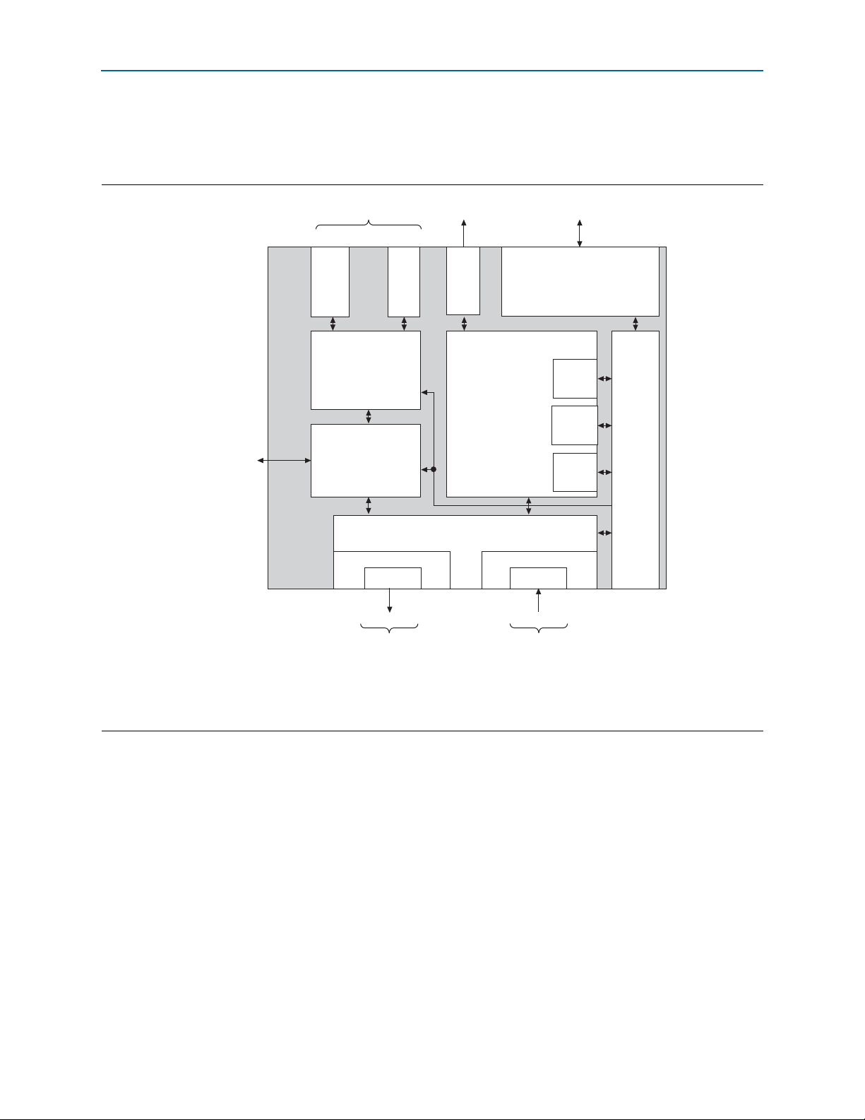
4–2 Chapter 4: Functional Description
AxC
IF
1
(1)
AxC
IF
24
(1)
...
CPU Interface Module
Registers
tx_dataout
IQ Data Channels
(Optional) CPU InterfaceMI Interface
Transmitter
Transceiver
Transmitter
rx_datain
CPRI LinkCPRI Link
Receiver
Transceiver
Receiver
Physical Layer
AUX Interface
Ethernet
(2)
MII
(2)
VSS/
Inband/
Alarms
HDLC
(3)
Control and Management
Module
CPRI MAP
Interface Module
RX Delay Measurement
and TX Calibration
Block
Architecture Overview
Architecture Overview
Figure 4–1 shows the main blocks of the CPRI IP core.
Figure 4–1. CPRI IP Core Block Diagram
Notes to Figure 4–1:
(1) You can configure your CPRI IP core with zero, one, or multiple IQ data channels.
(2) You can configure your CPRI IP core with an Ethernet MAC block or an MII block. The two options are mutually exclusive.
(3) You can configure your CPRI IP core with or without an HDLC block.
CPRI MegaCore Function December 2013 Altera Corporation
The Altera CPRI IP core supports the following interfaces:
■ MAP Interface
■ Auxiliary Interface
■ Media Independent Interface to an External Ethernet Block
■ CPU Interface
■ CPRI link interface described in CPRI Protocol Interface Layer (Physical Layer)
Information about the signals on the individual interfaces is available in the following
sections and in Chapter 6, Signals.
The following sections describe the individual interfaces and clocks.
User Guide
Page 35

Chapter 4: Functional Description 4–3
Clocking Structure
Clocking Structure
The CPRI IP core has a variable number of clock domains. The clock domains in your
CPRI IP core variation depend on the following factors:
■ Number of antenna-carrier interfaces.
■ Whether the MII is configured.
■ Whether the antenna-carrier interfaces are clocked internally. Refer to “Enable
Internally-Clocked Synchronization Mode” on page 3–7.
■ Targe t de vi ce fa mi ly.
■ In one case, different CPRI line rates.
The input clock frequency requirements depend on the target device family and CPRI
line rate. Refer to Table 4–2 on page 4–10 for these requirements.
You can configure a CPRI IP core in master or slave clocking mode, as described in
“Operation Mode Parameter” on page 3–2. REC configurations and RE master
configurations use master clocking mode, and RE slave configurations use slave
clocking mode. Your design must handle some of the transceiver input clocks
differently in the two different clocking modes. The clocking diagrams in “Clock
Diagrams for the CPRI IP Core” on page 4–5 describe the requirements.
The CPRI IP core supports dynamic switching between master and slave clocking
modes in Arria V, Cyclone V, and Stratix V devices. This section describes how to
connect the CPRI IP core input clock signals to support dynamic clock mode
switching and how to dynamically switch the clock mode in your CPRI IP core.
Tab le 4– 1 describes the individual clocks. The clocking diagrams in Figure 4–2 on
page 4–6 to Figure 4–4 on page 4–8 show the clocks and clock domain boundaries.
Table 4–2 on page 4–10 lists the clock frequencies for the different CPRI IP core
variations.
CPRI IP Core Clocks
Tab le 4– 1 describes the clock domains in the CPRI IP core.
For more information about these clocks, including driver requirements, refer to
Chapter 6, Signals. For expected input clock frequencies refer to Chapter 6, Signals
and to Table 4–2 on page 4–10.
Table 4–1. CPRI IP Core Clocks (Part 1 of 3)
Clock Name Direction
cpri_clkout
Output
Configuration
Requirements
Present in all
CPRI IP cores
Description
Main clock for the CPRI IP core. The CPRI IP core derives this clock
from the transceiver transmit PLL, and the frequency of this clock
depends on the CPRI line rate. For more information refer to “CPRI
Communication Link Line Rates” on page 4–10.
December 2013 Altera Corporation CPRI MegaCore Function
User Guide
Page 36

4–4 Chapter 4: Functional Description
Clocking Structure
Table 4–1. CPRI IP Core Clocks (Part 2 of 3)
Clock Name Direction
mapN_tx_clk
for N in
0..(N_MAP–1)
mapN_rx_clk
for N in
0..(N_MAP–1)
clk_ex_delay
cpri_mii_txclk
cpri_mii_rxclk
cpu_clk
gxb_refclk
gxb_cal_blk_clk
reconfig_clk
gxb_pll_inclk
pll_clkout
Input
Input
Input
Output
Output
Input
Input
Input
Input
Input
Output
Configuration
Requirements
Present in
variations
configured with
N_MAP > 0
antenna-carrier
interfaces and
with Enable MAP
interface
synchronization
with core clock
turned off
Present in all
CPRI IP cores
Present in
variations
configured with
an MI interface
Present in all
CPRI IP cores
Present in all
CPRI IP cores
Not present in
variations that
target an Arria V,
Cyclone V, or
Stratix V device
Present in all
CPRI IP cores
Present in all
CPRI IP cores
Present in all
CPRI IP cores
Description
Expected rate of received data on antenna-carrier interface N. The
frequency of this clock is the sample rate on the incoming
antenna-carrier interface. For more information about data channel
sample rates, refer to Table 4–5 and Table 4–6 on page 4–17.
Clocks the transmissions of antenna-carrier interface N. The
frequency of this clock is the sample rate on the outgoing
antenna-carrier interface. For more information about data channel
sample rates, refer to Table 4–5 and Table 4–6 on page 4–17.
Clock for extended delay measurement. For more information refer to
“Extended Rx Delay Measurement” on page E–6.
Clocks the MII transmitter module. This clock has the same
frequency as the
cpri_clkout
clock. The frequency depends on the
CPRI line data rate. Refer to “CPRI Communication Link Line Rates”
on page 4–10.
Clocks the MII receiver module. This clock has the same frequency as
the
cpri_clkout
clock. The frequency depends on the CPRI line
data rate. Refer to “CPRI Communication Link Line Rates” on
page 4–10.
Controls the input to the CPU interface of the CPRI IP core and drives
the CPU interface. Assumed to be asynchronous with the
cpri_clkout
clock. The maximum frequency is constrained by f
MAX
and can vary based on the device family and speed grade.
Reference clock for the transceiver PLLs. In master clocking mode,
this clock drives both the receiver PLL and the transmitter PLL in the
transceiver. In slave clocking mode, this clock drives the receiver
PLL.
In master clocking mode, you must tie this input to the same source
as
gxb_pll_inclk
.
Transceiver calibration-block clock.
Transceiver dynamic reconfiguration block clock.
Input clock to the transmitter PLL in a CPRI IP core configured in
slave clocking mode. In master clocking mode, you must tie this
input to the same source as
gxb_refclk
.
Generated from transceiver clock data recovery circuit. Intended to
connect to an external PLL for jitter clean-up in slave clocking mode.
CPRI MegaCore Function December 2013 Altera Corporation
User Guide
Page 37

Chapter 4: Functional Description 4–5
Clocking Structure
Table 4–1. CPRI IP Core Clocks (Part 3 of 3)
Clock Name Direction
usr_pma_clk
usr_clk
Clock Diagrams for the CPRI IP Core
Input
Input
Configuration
Requirements
Present in
variations
configured at
9830.4 Gbps that
target an
Arria V GT device
Extra clock signal required to drive the PMA in these CPRI IP core
variations. Refer to Table 6–15 on page 6–17 for driver frequency and
synchronization requirements.
Extra clock signal required to drive the PCS in these CPRI IP core
variations. Refer to Table 6–15 on page 6–17 for driver frequency and
synchronization requirements.
Description
Figure 4–2 and Figure 4–3 show the clocking schemes for CPRI IP cores configured as
RE slaves, RE masters, and REC masters that do not target an Arria V GT device or
that are not configured with a CPRI line rate of 9830.4 Mbps.
Figure 4–4 on page 4–8 and Figure 4–5 on page 4–9 show the clocking schemes for
CPRI IP cores configured as RE slaves, RE masters, and REC masters with a CPRI line
rate of 9830.4 Mbps that target an Arria V GT device. These variations have no clock
divider and no Tx elastic buffer or Rx elastic buffer. However, they require two
additional synchronized input clocks,
usr_pma_clk and usr_clk.
You must drive the usr_pma_clk and usr_clk clocks at the , which you must drive at
the frequency of 122.88 MHz, and
usr_clk,
which you must drive at the frequency of
245.76 MHz.
December 2013 Altera Corporation CPRI MegaCore Function
User Guide
Page 38

4–6 Chapter 4: Functional Description
Transceiver
CPRI TX
MII Interface
CPU
Interface
Rx Elastic
Sync Buffer
Tx Elastic
Sync Buffer
CPRI RX
CDR
FIFO
Buffer
CPRI MegaCore Function
Clock
Divider
(1)
Clean-Up PLL
cpu_clk
gxb_pll_inclkpll_clkout
tx_clkout
cpri_clkout
cpri_clkout
Clock
Domain
rx_clkout
gxb_refclk
mapN_tx_clk
clk_ex_delay
FIFO
Buffer
mapN_rx_clk
CPRI Rx
MAP
Interface
CPRI Tx
MAP
Interface
cpri_mii_txclk
cpri_mii_rxclk
Clocking Structure
Clock Diagrams for Most CPRI IP Core Variations
Figure 4–2 shows the clock diagram for a CPRI IP core configured as an RE slave,
unless the IP core is configured with CPRI line rate 9.830.4 Mbps and targets an
Arria V GT device.
Figure 4–2. CPRI IP Core Slave Clocking Except for Arria V GT 9.8 Gbps Variations
Note to Figure 4–2:
(1) The clock divider factor depends on the device family. In device families with a factor of 1, the divider is not configured. Table 4–17 on page 4–59
lists the datapath width and clock divider by device family.
CPRI MegaCore Function December 2013 Altera Corporation
User Guide
Page 39
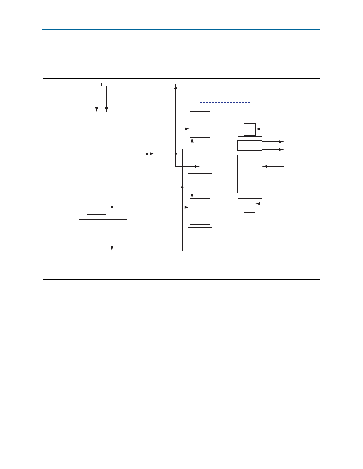
Chapter 4: Functional Description 4–7
Transceiver
CPRI TX
MII Interface
CPU
Interface
Rx Elastic
Sync Buffer
Tx Elastic
Sync Buffer
CPRI RX
CDR
FIFO
Buffer
CPRI MegaCore Function
Clock
Divider
(1)
cpu_clk
gxb_pll_inclk
pll_clkout
tx_clkout
cpri_clkout
cpri_clkout
Clock
Domain
rx_clkout
gxb_refclk
mapN_tx_clk
clk_ex_delay
FIFO
Buffer
mapN_rx_clk
CPRI Rx
MAP
Interface
CPRI Tx
MAP
Interface
cpri_mii_txclk
cpri_mii_rxclk
Clocking Structure
Figure 4–3 shows the clock diagram for a CPRI IP core configured as an REC master
or as an RE master, unless the IP core is configured with CPRI line rate 9830.4 Mbps
and targets an Arria V GT device.
Figure 4–3. CPRI IP Core Master Clocking Except for Arria V GT 9.8 Gbps Variations
Note to Figure 4–3:
(1) The clock divider factor depends on the device family. In device families with a factor of 1, the divider is not configured. Table 4–17 on page 4–59
lists the datapath width and clock divider by device family.
Clock Diagrams for CPRI IP Core Arria V GT Variations at 9830.4 Mbps
CPRI IP core variations configured with a CPRI line rate of 9830.4 Mbps that target an
December 2013 Altera Corporation CPRI MegaCore Function
Arria V GT device have a different clocking scheme. These variations have no clock
divider, and have neither an RX elastic buffer nor a TX elastic buffer.
These variations use two additional input clock signals,
Table 6–15 on page 6–17 describes the requirements for these two input clock signals.
When a variation configured with a CPRI line rate of 9830.4 Mbps that targets an
Arria V GT device participates in autorate negotiation, you must modify the
frequency of the
different CPRI line rates. Refer to Appendix B, Implementing CPRI Link Autorate
Negotiation.
usr_clk
and
usr_pma_clk
usr_clk
input clocks to specific values for the
and
usr_pma_clk
User Guide
.
Page 40

4–8 Chapter 4: Functional Description
CPRI MegaCore Function
clk_ex_delaypll_clkout
cpri_clkoutusr_clk
(245.76 MHz)
usr_pma_clk
(122.88 MHz)
gxb_refclk
gxb_pll_inclk
tx_clkout
TX
Buffer
RX
Buffer
data
32
32
80
80
80
80
32
data
32
122.88 MHz
122.88 MHz
Soft
PCS
Soft
PCS
tx_clkout
rx_clkout
Transceiver
Native PHY
IP Core
CPRI TX
MII Interface
CPU
Interface
CPRI RX
FIFO
Buffer
cpu_clk
cpri_clkout
Clock
Domain
mapN_tx_clk
FIFO
Buffer
mapN_rx_clk
CPRI Rx
MAP
Interface
CPRI Tx
MAP
Interface
cpri_mii_txclk
cpri_mii_rxclk
Clean-Up PLL
Clocking Structure
Figure 4–4 shows the clocking scheme for a CPRI IP core that targets an Arria V GT
device and is configured with a CPRI line rate of 9830.4 Mbps, configured or
programmed as an RE slave.
Figure 4–4. CPRI IP Core Slave Clocking in Arria V GT 9.8 Gbps Variations
(1)
Notes to Figure 4–4:
(1) In slave clocking mode, the
usr_clk
and
usr_pma_clk
input clocks must be driven by a common source from the cleanup PLL. For additional
constraints these clocks require, refer to Table 6–15 on page 6–17.
CPRI MegaCore Function December 2013 Altera Corporation
User Guide
Page 41
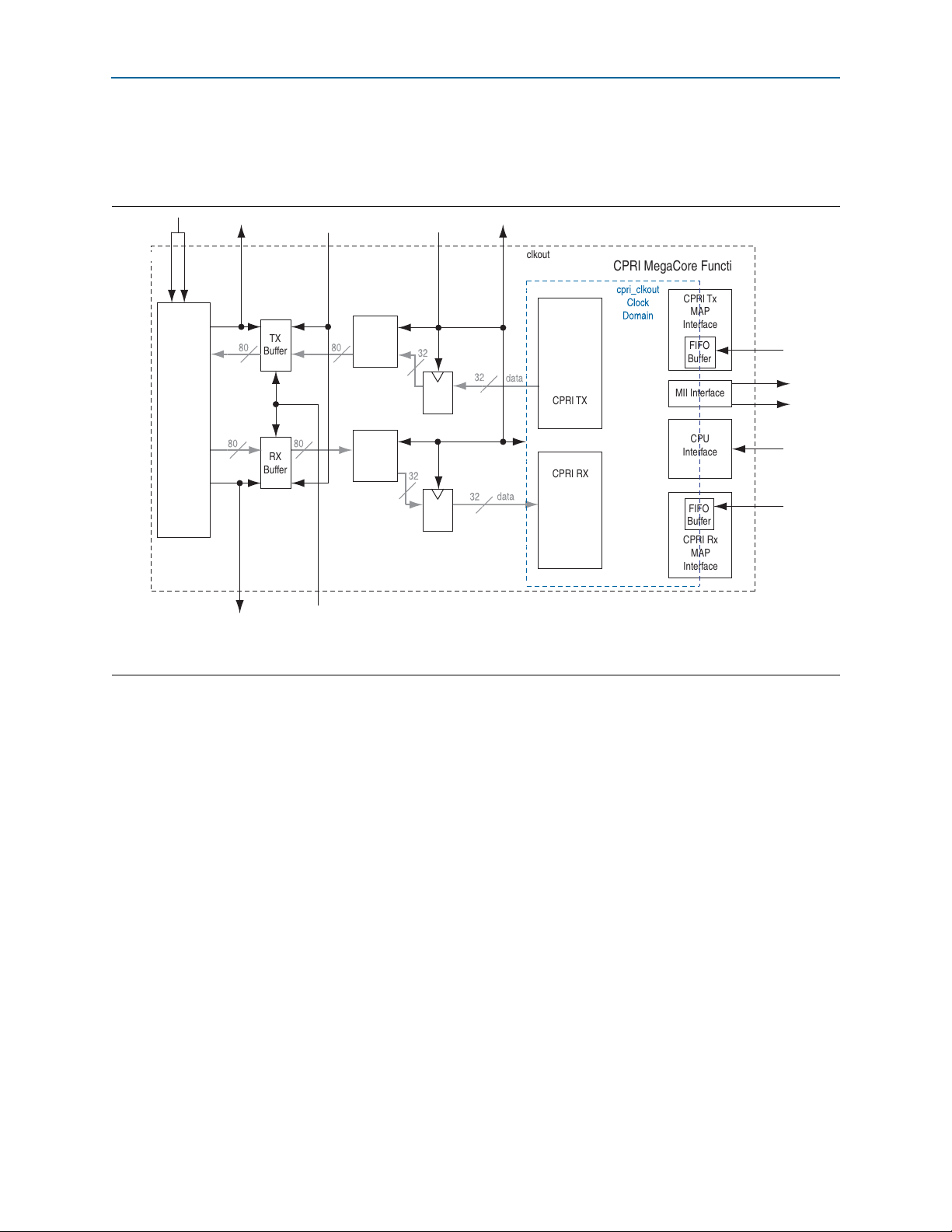
Chapter 4: Functional Description 4–9
CPRI MegaCore Function
clk_ex_delaypll_clkout
cpri_clkoutusr_clk
(245.76 MHz)
usr_pma_clk
(122.88 MHz)
gxb_refclk gxb_pll_inclk tx_clkout
TX
Buffer
RX
Buffer
data
32
32
80
80
80 80
32
data
32
122.88 MHz
122.88 MHz
Soft
PCS
Soft
PCS
tx_clkout
rx_clkout
Transceiver
Native PHY
IP Core
CPRI TX
MII Interface
CPU
Interface
CPRI RX
FIFO
Buffer
cpu_clk
cpri_clkout
Clock
Domain
mapN_tx_clk
FIFO
Buffer
mapN_rx_clk
CPRI Rx
MAP
Interface
CPRI Tx
MAP
Interface
cpri_mii_txclk
cpri_mii_rxclk
Clocking Structure
Figure 4–5 shows the clocking scheme for a CPRI IP core that targets an Arria V GT
device and is configured with a CPRI line rate of 9830.4 Mbps, configured or
programmed as an REC or RE master.
Figure 4–5. CPRI IP Core Master Clocking in Arria V GT 9.8 Gbps Variations
Notes to Figure 4–5:
(1) In master clocking mode, you must drive the
gxb_pll_inclk
and
gxb_refclk
input signals from a common source.
(1)
December 2013 Altera Corporation CPRI MegaCore Function
Dynamically Switching Clock Mode
The CPRI IP core supports dynamic clock mode switching in variations that target an
Arria V, Cyclone V, or Stratix V device, from master clock mode to slave clock mode
and from slave clock mode to master clock mode. The value you select for Operation
mode in the CPRI parameter editor determines the clock mode in which the IP core is
configured initially. However, you can modify this value dynamically.
To switch the clock mode of your Arria V, Cyclone V, or Stratix V CPRI IP core,
perform the following steps:
1. Ensure your design supports the input clock connection requirements for the clock
mode to which you intend to switch the IP core.
2. Implement the clock connection requirements for the intended new clock mode by
switching the source that drives the
Diagrams for the CPRI IP Core” on page 4–5.
3. Write the new value to the
Table 7–6 on page 7–4 for the appropriate value.
4. Wait until you observe successful CPRI link resynchronization. Refer to
Appendix A, Initialization Sequence.
operation_mode
gxb_pll_inclk
bit of the
signal. Refer to “Clock
CPRI_CONFIG
register. Refer to
User Guide
Page 42

4–10 Chapter 4: Functional Description
Clocking Structure
CPRI Communication Link Line Rates
The CPRI specification specifies line rates of n × 614.4 Mbps for various values of n.
The CPRI IP core supports different ranges of line rates in different device families.
Table 3–1 on page 3–2 lists the CPRI line rate support available in the different device
families.
Tab le 4– 2 shows the relationship between line rates, default transceiver reference
clock (
clock (
gxb_refclk
cpri_clkout
) rates, parallel recovered clock (
) rates.
pll_clkout
) rates, and internal
Table 4–2. CPRI Link Line Rates and Clock Rates for CPRI MegaCore Function
(1)
Clock Frequency (MHz)
Default gxb_refclk Frequency
(If line rate is supported)
Line Rate
(Mbps)
Arria II GX
Arria II GZ
and
Cyclone IV GX
Devices
Stratix IV GX
Devices
614.4 61.44 61.44
and
Arria V
Cyclone V
and
Stratix V
Devices
cpri_clkout
Frequency
(If line rate
is
supported)
Arria II GX
and
Cyclone IV GX
Devices
15.36 61.44 61.44 61.44 —
pll_clkout Frequency
(If line rate is supported)
Arria II GZ
and
Stratix IV GX
Devices
Arria V
Cyclone V
and
Stratix V
Devices
(2)
Configured
Arria V GT
Devices
at 9830.4
Mbps
1228.8 61.44 61.44 30.72 61.44 30.72 30.72 61.44
2457.6 122.88 61.44 61.44 122.88 61.44 61.44 122.88
3072 153.60 76.80 76.80 153.60 76.80 76.80 153.6
(4)
4915.2
(4)
6144
(5)
9830.4
Notes to Table 4–2:
(1) In this table, device families can be grouped with other device families that do not support all of the same CPRI line rates. The values apply only for
supported CPRI line rates for each device family.
(2) This column lists the
a CPRI line rate less than 9803.4 Mbps.
(3) The value of
frequency parameter value that you set in the CPRI parameter editor.
(4) The CPRI IP core does not support CPRI line rates 4915.2 Mbps and 6144 Mbps in variations that target Cyclone IV GX or Cyclone V GX devices.
(5) The CPRI IP core supports CPRI line rate 9830.4 Mbps in variations that target Stratix V (GX or GT), Arria V GT, or Arria V GZ devices. The CPRI IP
core does not support CPRI line rate 9830.4 Mbps for any other devices, including Arria V GX devices.
245.76 122.88 122.88 245.76 122.88 122.88 61.44
307.20 153.60 153.60 307.20 153.60 153.60 76.8
— — 245.76 — — 245.76 122.88
pll_clkout
gxb_refclk
frequencies for Arria V GX and Arria V GZ devices, as well as Arria V GT devices that are originally configured at
in CPRI IP cores that target a 28-nm device (Arria V, Cyclone V, or Stratix V device) is the Transceiver reference clock
(3)
cpri_clkout
The
frequency depends only on the CPRI line rate. The
pll_clkout
frequency depends on the CPRI line rate and on the datapath width through the
transceiver, except in Arria V, Cyclone V, and Stratix V devices. The
pll_clkout
frequency in an Arria V GT device depends on whether the IP core was originally
configured with the CPRI line rate of 9.8304 Gbps, and whether or not the IP core
CPRI line rate is modified dynamically through auto-rate negotiation. The datapath
width is determined by device family, as shown in Table 4–17 on page 4–59.
The
gxb_refclk
Altera allows you to program the transceiver to work with any of a set of
clock is the incoming reference clock for the device transceiver’s PLL.
gxb_refclk
frequencies that the PLL in the transceiver can convert to the required internal clock
speed for the CPRI IP core line rate. The parameter editor in which you configure the
gxb_refclk
frequency depends on the target device family for your CPRI IP core
variation.
CPRI MegaCore Function December 2013 Altera Corporation
User Guide
Page 43

Chapter 4: Functional Description 4–11
Reset Requirements
When you generate a CPRI IP core variation that targets an Arria II, Cyclone IV GX, or
Stratix IV GX device, you generate an ALTGX megafunction with specific default
settings. These default transceiver settings configure a transceiver that works
correctly with the CPRI IP core when the input
gxb_refclk
clock has the frequency
shown in Tab le 4– 2. However, you can edit the ALTGX megafunction instance to
specify a different
example, to enable you to use an existing clock in your system as the
gxb_refclk
frequency that is more convenient for your design, for
gxb_refclk
reference clock.
When you generate a CPRI IP core variation that targets an Arria V, Cyclone V, or
Stratix V device, you generate an Altera Deterministic Latency PHY IP core or Altera
Native PHY IP core with specific default settings. However, you set the
gxb_refclk
frequency in the CPRI parameter editor. As described in Chapter 3, Parameter
Settings, for these target devices the CPRI parameter editor provides a list of potential
transceiver reference clock frequencies from which you select the frequency that is
most convenient for your design.
Reset Requirements
The CPRI IP core has multiple independent reset signals.To reset the CPRI IP core
completely, you must assert all the reset signals.
You can assert all reset signals asynchronously to any clock. However, each reset
signal must be asserted for at least one full clock period of a specific clock, and be
deasserted synchronously to the rising edge of that clock. For example, the CPU
interface reset signal,
cpu_reset
, must be deasserted on the rising edge of
cpu_clk
Tab le 4– 3 lists the reset signals and their corresponding clock domains.
Table 4–3. Reset Signals and Corresponding Clock Domains
Reset Signal Clock Domain Description
reset reconfig_clk
gxb_powerdown
reset_ex_delay clk_ex_delay
config_reset cpri_clkout
cpu_reset cpu_clk
mapN_rx_reset mapN_rx_clk
mapN_tx_reset mapN_tx_clk
—
Resets the CPRI protocol interface. Drives the
reset controller.
Powers down and resets the high-speed
transceiver block. For setup and hold times,
refer to the relevant device handbook. This
signal is not present in CPRI IP core variations
that target an Arria V, Cyclone V, or Stratix V
device.
Resets the extended delay measurement block.
Resets the registers to their default values.
Resets the CPU interface.
Resets the MAP Channel N receiver block in
FIFO or synchronous buffer MAP
synchronization mode.
Resets the MAP Channel N transmitter block in
FIFO or synchronous buffer MAP
synchronization mode.
.
December 2013 Altera Corporation CPRI MegaCore Function
User Guide
Page 44

4–12 Chapter 4: Functional Description
DDQ
Q
rstrst
clk
rst
reset
CPRI
MegaCore
Function
MAP Interface
You must implement logic to ensure the minimal hold time and synchronous
deassertion of each reset input signal to the CPRI IP core. Figure 4–6 shows a circuit
that ensures these conditions for one reset signal.
Figure 4–6. Circuit to Ensure Synchronous Deassertion of Reset Signal
For more information about the requirements for reset signals, refer to Chapter 6,
Signals.
The CPRI IP core has a dedicated reset control module to enforce the specific reset
requirements of the high-speed transceiver module. This reset controller generates the
recommended reset sequence for the transceiver. The
reset
signal controls the reset
control module.
MAP Interface
f For information about the Avalon-ST interface, refer to Avalon Interface Specifications.
In Arria V, Cyclone V, and Stratix V devices, the Altera Deterministic Latency PHY IP
core or Altera Native PHY IP core that is generated with the CPRI IP core implements
the reset controller. In earlier device families, the reset control module is internal to
the CPRI IP core, but external to the ALTGX megafunction instance generated with
the CPRI IP core.
After reset, your software must perform link synchronization and other initialization
tasks. For information about the required initialization sequence following CPRI IP
core reset, refer to Appendix A, Initialization Sequence.
The CPRI IP core MAP interface comprises the individual antenna-carrier interfaces,
or data channels, through which the CPRI IP core transfers IQ sample data to and
from the RF implementation. The MAP interface is implemented as an incoming and
an outgoing Avalon-ST interface. The Avalon-ST interface provides a standard,
flexible, and modular protocol for data transfers from a source interface to a sink
interface.
CPRI MegaCore Function December 2013 Altera Corporation
User Guide
Page 45

Chapter 4: Functional Description 4–13
MAP Interface
The CPRI IP core communicates with the RF implementations (antenna-carriers)
through multiple AxC interfaces, or data channels. A CPRI IP core configured with a
MAP interface module can have as many as 24 data channels, and as few as one data
channel. If a CPRI IP core is configured with zero data channels, it does not have a
MAP interface module. The Number of antenna/carrier interfaces value you set in
the parameter editor determines the number of channels in your CPRI IP core
configuration. Each data channel communicates with the corresponding RF
implementation using two 32-bit Avalon-ST interfaces, one interface for incoming
communication and one interface for outgoing communication.
The MAP interface module controls transmission and reception of data on the AxC
interfaces.
1 The MAP interface does not support GSM mapping. You must implement this CPRI
V5.0 Specification feature using the CPRI IP core AUX interface.
This section contains the following topics:
■ MAP Interface Mapping Modes
■ MAP Receiver Interface
■ MAP Transmitter Interface
MAP Interface Mapping Modes
The CPRI IP core supports basic and advanced MAP interface mapping modes.
In the basic mapping mode, all of the AxC interfaces use the same sample rate and
sample width, and the uplink and downlink sample rates are identical.
In the advanced mapping modes, different data channels can use different sample
rates, and the sample rates need not be integer multiples of 3.84 MHz. However, all
data channels use the same sample width.
If you select All as the value for Mapping mode(s) in the CPRI parameter editor, the
map_mode
CPRI IP core implements currently. Otherwise, the value you specify for this
parameter determines the single mapping mode your CPRI IP core implements.
Tab le 4– 4 lists the MAP interface mapping modes the CPRI IP core supports and how
to configure or program your IP core in each mapping mode.
Table 4–4. Determining the MAP Interface Mapping Mode (Part 1 of 2)
Basic Don’t Care
All 2’b00
field of the
Mapping mode(s)
Parameter Value
CPRI_MAP_CONFIG
register determines the mapping mode your
Value Programmed in
map_mode field of
CPRI_MAP_CONFIG
Register
Mapping
Mode
Basic In current section
Mode Description
December 2013 Altera Corporation CPRI MegaCore Function
User Guide
Page 46

4–14 Chapter 4: Functional Description
Table 4–4. Determining the MAP Interface Mapping Mode (Part 2 of 2)
Value Programmed in
Mapping mode(s)
Parameter Value
Advanced 1 Don’t Care
All 2’b01
Advanced 2 Don’t Care
All 2’b10
Advanced 3 Don’t Care
All 2’b11
map_mode field of
CPRI_MAP_CONFIG
Register
Mapping
Mode
Advanced 1
Advanced 2
Advanced 3
Mode Description
Appendix D, Advanced
AxC Mapping Modes
MAP Interface
Configuring your IP core with the All mapping mode provides you the flexibility to
modify the mapping mode dynamically, but configuring your IP core with the specific
mapping mode you expect to use generates a smaller IP core.
Basic AxC Mapping Mode
The basic mapping mode supports the LTE/E-UTRA and UMTS/WCDMA
standards. This mapping mode is implemented when you configure and program
your CPRI IP core in either of the following ways:
■ If you select Basic as the value for Mapping mode(s) in the CPRI parameter editor.
■ If you select All as the value for Mapping mode(s) in the CPRI parameter editor
and you program the
map_mode
field of the
CPRI_MAP_CONFIG
register with the
value of 2’b00.
In this basic mapping mode, all of the AxC interfaces use the same sample rate and
sample width. The CPRI IP core supports sample rates of 3.84 × 10
30.72 × 10
6
(3.84 × 106× 8) samples per second, in increments of 3.84 × 10⁶, and sample
6
through
widths of 15 bits and 16 bits. The uplink and downlink sample rates are identical.
In this mode, the
map_ac
field of the
CPRI_MAP_CNT_CONFIG
register specifies the
number of active data channels, that is, those that have a corresponding AxC
container in the IQ data block of each basic frame. This number must be less than or
equal to the N_MAP value you selected for Number of antenna/carrier interfaces in
the parameter editor, which is the number of channels configured in the CPRI IP core
instance. The
map_n_ac
field of the
CPRI_MAP_CNT_CONFIG
register holds the
oversampling factor for the data channels. This value is an integer from 1 to 8. The
sample rate—number of samples per second—is the product of 3.84 × 10
6
and the
oversampling factor.
CPRI MegaCore Function December 2013 Altera Corporation
User Guide
Page 47
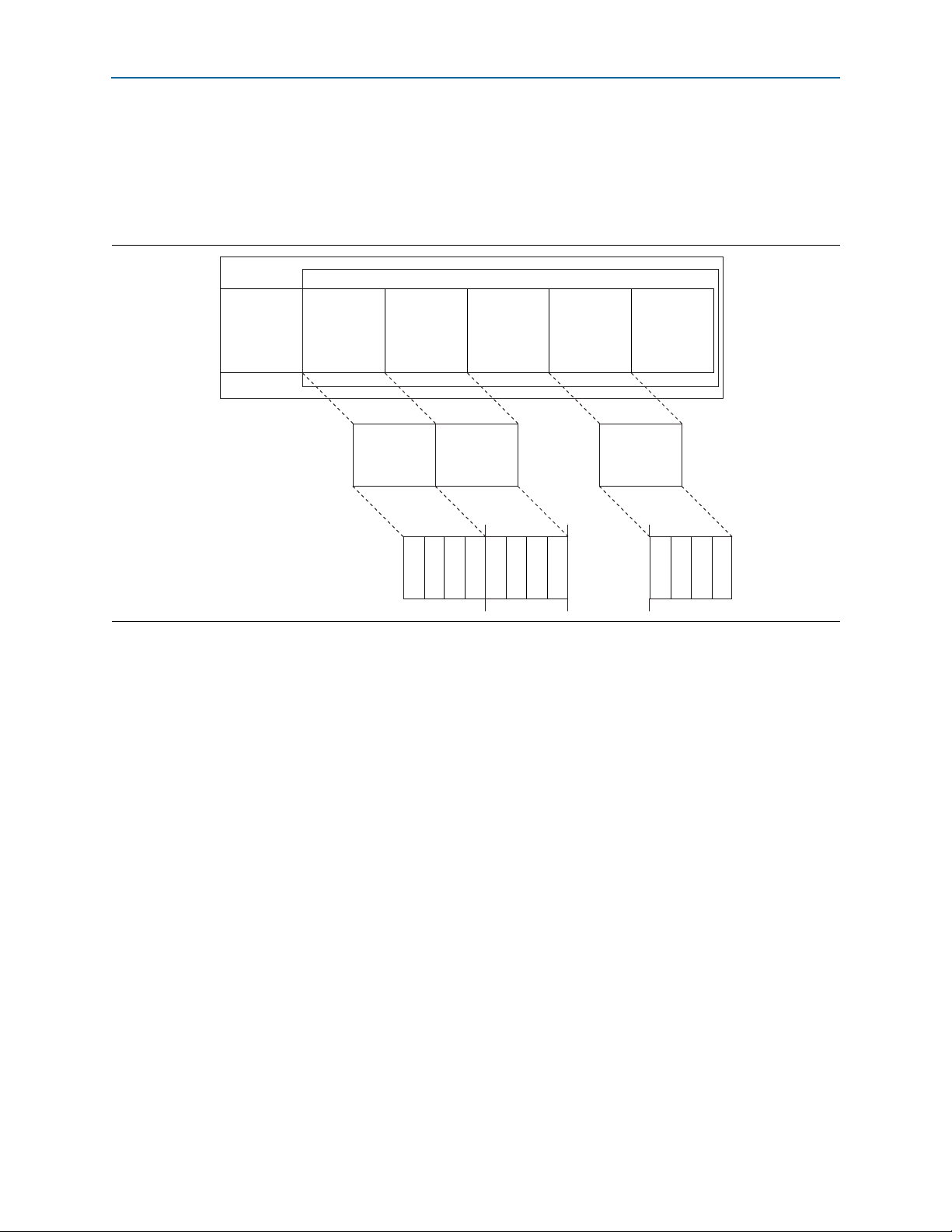
Chapter 4: Functional Description 4–15
Control
Words
AxC
Container
1
AxC
Container
2
...
...
AxC
Container
map_ac
Reserved
Bits
IQ Data Block
Basic Frame
AxC
Interface
0
Data
AxC
Interface
1
Data
AxC
Interface
map_ac
Data
...
Data Word 1
Data Word 2
Data Word
map_n_ac
...
Data Word 1
Data Word 2
Data Word
map_n_ac
...
Data Word 1
Data Word 2
Data Word
map_n_ac
...
MAP Interface
In the basic mapping mode, AxC containers are packed in the IQ data block in the
packed position (Option 1) illustrated in Section 4.2.7.2.3 of the CPRI V4.2
Specification. Figure 4–7 shows how the AxC containers map to the individual active
data channels. The oversampling factor is the number of 32-bit data words in each
AxC container.
Figure 4–7. CPRI Basic Mapping Mode
1 The CPRI IP core does not support AxC interface reordering. When the value of
map_ac
is less than N_MAP, the first
map_ac
AxC interfaces, of the existing N_MAP
interfaces, are active. Note that an active AxC interface transmits and receives data on
its data channel based on the values of the relevant
CPRI_IQ_RX_BUF_CONTROL
CPRI_IQ_TX_BUF_CONTROL
register and the relevant
register. Any data in an AxC container for an active but
map_rx_enable
map_tx_enable
bit of the
bit of the
disabled channel is ignored, and an incoming AxC container designated from a
disabled channel is ignored.
The
map_15bit_mode
field of the
CPRI_MAP_CONFIG
register specifies the sample width.
The sample width is the number of significant bits —15 or 16—in each 16-bit half
(originally, I- or Q-sample) of the 32-bit data word on the Avalon-ST data channel. In
15-bit mode, the least significant bit in each half of the 32-bit word is ignored when
received from the data channel on input signal
when transmitted on the data channel in output signal
Therefore, bit 15 and bit 31 of the data word correspond to bit 14 of the I and Q
samples, respectively; bit 1 and bit 17 of the data word correspond to bit 0 of the I and
Q samples, respectively; and bits 0 and 16 of the data word are ignored. In 16-bit
mapN_tx_data[31:0]
mapN_rx_data[31:0]
, and is set to 0
mode, bit 15 and bit 31 of the data word correspond to bit 15 of the I and Q samples,
respectively, and bit 0 and bit 16 of the data word correspond to bit 0 of the I and Q
samples, respectively. Figure 4–8 shows the bit correspondence for both sample
widths.
.
December 2013 Altera Corporation CPRI MegaCore Function
User Guide
Page 48

4–16 Chapter 4: Functional Description
MAP Interface
Figure 4–8. Bit Correspondence Between IQ Sample and 32-Bit Avalon-ST Data
16-Bit Width IQ Sample:
Q: I:
15 1 0 15 2 1 0
Avalon-ST Data Word in AxC Container:
31 17 16 15 2 1 0
15-Bit Width IQ Sample:
Q: I:
14 0 14 210
You set the oversampling factor to match the frequency of your active data channels.
The CPRI line rate determines the number of bits in the IQ data block of each basic
frame. If your CPRI IP core has a high line rate and a low oversampling factor, it can
accommodate a larger number of active data channels than if the line rate were lower
or the oversampling factor higher.
In 15-bit mode, inside the CPRI IP core, bits 0 and 16 of the Avalon-ST data are absent
from the compact IQ data word representation. Therefore, despite the fact that in
15-bit mode the IQ data goes out on the data channel in 32-bit words, formatted as
CPRI MegaCore Function December 2013 Altera Corporation
User Guide
Page 49

Chapter 4: Functional Description 4–17
MAP Interface
shown in Figure 4–8, the maximum number of active data channels is higher in 15-bit
mode. Table 4–5 shows the correspondence between these frequency factors in 16-bit
mode, and Table 4–6 shows the correspondence between these factors in 15-bit mode.
Table 4–5. Maximum Number of Active Data Channels in 16-Bit Mode
Maximum Number of Active Data Channels in 16-Bit Mode
CPRI
Line Rate
(Mbps)
Number of Bits
in
IQ Data Block
Data Channel
Bandwidth LTE
(MHz)
Sample Rate
6
Sample/Sec)
(10
2.5 5 10 15 20
3.84 7.68 15.36 23.04 30.72
614.4 120 3 1 — — —
1228.8 240 7321—
2456.7 480 15 7321
3072 600 189432
4915.2 960 30
6144 1200 37
9830.4 1920 60
Note to Table 4–5:
(1) The maximum number of data channels supported by the CPRI IP core is 24. The numbers in the table that are larger than 24 are hypothetical;
the CPRI IP core cannot implement them.
(1)
(1)
(1)
15753
18964
(1)
30
15 10 7
Table 4–6. Maximum Number of Active Data Channels in 15-Bit Mode
Maximum Number of Active Data Channels in 15-Bit Mode
CPRI
Line Rate
(Mbps)
Number of Bits
in
IQ Data Block
Data Channel
Bandwidth LTE
2.5 5 10 15 20
(MHz)
Sample Rate
6
Sample/Sec)
(10
3.84 7.68 15.36 23.04 30.72
614.4 120 4 2 1 — —
1228.8 240 84211
2456.7 480 16 8422
3072 600 20 10 5 3 2
4915.2 960 32
6144 1200 40
9830.4 1920 64
Note to Table 4–6:
(1) The maximum number of data channels supported by the CPRI IP core is 24. The numbers in the table that are larger than 24 are hypothetical;
the CPRI IP core cannot implement them.
(1)
(1)
(1)
16854
20 10 6 5
(1)
32
16 10 8
In 16-bit mode, the total number of bits in all the AxC containers in a basic frame is
2 × 16 ×
map_n_ac
×
map_ac
In 15-bit mode, the total number of bits in all the AxC containers in a basic frame is
2 × 15 ×
December 2013 Altera Corporation CPRI MegaCore Function
map_n_ac
×
map_ac
User Guide
Page 50

4–18 Chapter 4: Functional Description
MAP Interface
This value must be no larger than the number of bits in the IQ data block. The number
of bits in an IQ data block depends on the CPRI line rate, as shown in Tab le 4– 5 and
Tab le 4– 6.
1 If the combination of CPRI line rate,
data bits than the number of data bits that fit in the IQ data block, the data for the first
active data channels is transferred correctly, but the data for data channels beyond the
number indicated in Tab le 4 –5 or Tab le 4– 6 is not transferred correctly.
The following CPRI IP core registers are ignored in basic mapping mode:
■
CPRI_MAP_TBL_CONFIG
■
CPRI_MAP_TBL_INDEX
■
CPRI_MAP_TBL_RX
■
CPRI_MAP_TBL_TX
register (Table 7–33 on page 7–17)
register (Table 7–34 on page 7–17)
register (Table 7–35 on page 7–17)
register (Table 7–36 on page 7–18)
Advanced AxC Mapping Modes
The CPRI IP core provides advanced AxC mapping modes to support the following
mapping methods from the CPRI V4.2 Specification:
■ Method 1: IQ Sample Based, described in Section 4.2.7.2.5 of the CPRI V4.2
Specification.
■ Method 3: Backward Compatible, described in Section 4.2.7.2.7 of the CPRI V4.2
Specification.
In the advanced mapping modes, different data channels can use different sample
rates, and the sample rates need not be integer multiples of 3.84 MHz. However, all
data channels use the same sample width.
map_n_ac
value, and
map_ac
value requires more
Your CPRI IP core implements one of the advanced AxC mapping modes when you
configure and program your CPRI IP core in any of the following ways:
■ If you select Advanced 1, Advanced 2, or Advanced 3 as the value for Mapping
mode(s) in the CPRI parameter editor.
■ If you select All as the value for Mapping mode(s) in the CPRI parameter editor
and you program the
value of 2’b01, 2’b10, or 2’b11.
For more information about the advanced AxC mapping modes in the Altera CPRI IP
core, refer to Appendix D, Advanced AxC Mapping Modes. For information about
how to program the individual advanced mapping modes, refer to Table 4– 4 o n
page 4–13.
MAP Receiver Interface
The CPRI IP core MAP receiver interface presents the IQ data that the CPRI IP core
unloads from the CPRI frame received on the CPRI link. The MAP receiver
implements an Avalon-ST interface protocol. Refer to “MAP Receiver Signals” on
page 6–1 for details of the interface communication signals.
map_mode
field of the
CPRI_MAP_CONFIG
register with the
CPRI MegaCore Function December 2013 Altera Corporation
User Guide
Page 51

Chapter 4: Functional Description 4–19
MAP Interface
The MAP receiver interface presents the IQ data on each antenna-carrier interface
according to one of three different synchronization modes. The synchronization mode
is determined by your selection in the CPRI parameter editor and by the value you
program in the
map_rx_sync_mode
field of the
CPRI_MAP_CONFIG
register (Table 7–31 on
page 7–15), as shown in Tab le 4 –7 .
Table 4–7. MAP Rx Synchronization Mode Determined by CPRI_MAP_CONFIG Register Bits
SYNC_MAP
(1)
map_rx_sync_mode
(register bit [2])
Rx Synchronization Mode
0 0 FIFO mode (page 4–20)
0 1 Synchronous buffer mode (page 4–21)
1—
Notes to Table 4–7:
(1) You determine the value of SYNC_MAP when you generate your CPRI IP core. Refer to Chapter 3, Parameter
Settings.
(2) When SYNC_MAP has the value of 1, the value in the
is ignored.
(2)
Internally-clocked mode (page 4–23)
map_rx_sync_mode
bit of the
CPRI_MAP_CONFIG
register
Tab le 4– 8 lists the clocks for the AxC interfaces in the different Rx synchronization
modes.
Table 4–8. MAP Rx Interface Clocks Determined by Rx Synchronization Mode
Rx Synchronization Mode AxC Channel Clocks
FIFO mode
Synchronous buffer mode
Internally-clocked mode
Each AxC Rx interface is clocked by its own
mapN_rx_clk
driven by the application.
Every AxC interface is clocked by the CPRI IP core clock,
cpri_clkout
.
clock
You determine the AxC interface clocks when you turn the Enable MAP interface
synchronization with core clock parameter on (SYNC_MAP = 1) or off (SYNC_MAP
= 0) in the CPRI parameter editor before you generate your CPRI IP core.
MAP Receiver Interface Signals in Different Synchronization Modes
The different CPRI IP core MAP synchronization modes use different interface
signals. Tab le 4 –9 lists the MAP receiver interface signals used in each of these modes.
Table notes indicate the correct interpretation of the different symbols.
(1)
Table 4–9. MAP Receiver Interface Signals by Synchronization Mode
Available in Synchronization Mode
Signal Name Direction
FIFO
map{23…0}_rx_clk
map{23…0}_rx_reset
map{23…0}_rx_ready
map{23…0}_rx_data[31:0]
map{23…0}_rx_valid
map{23…0}_rx_resync
December 2013 Altera Corporation CPRI MegaCore Function
Input vv—
Input vv—
Input v 1
Output vvv
Output v —
Input —
(2)
(Part 1 of 2)
Synchronous
Buffer
(3)
(2)
v —
Internally
Clocked
(2)
(2)
(2), (4)
—
v
(2)
User Guide
Page 52

4–20 Chapter 4: Functional Description
MAP Interface
Table 4–9. MAP Receiver Interface Signals by Synchronization Mode
(1)
(Part 2 of 2)
Available in Synchronization Mode
Signal Name Direction
FIFO
map{23…0}_rx_start
map{23…0}_rx_status_data
[2:0]
Notes to Table 4–9:
(1) A checkmark indicates the signal is used in a synchronization mode, and a dash indicates the signal is not used in
that synchronization mode.
(2) An entry with a dash indicates a signal that does not participate in the MAP receiver interface communication in
this synchronization mode. The signal is either not present in the configuration or is ignored. An input signal that
is ignored is ignored by the CPRI IP core. An output signal that is ignored should be ignored by the application.
Refer to Table 6–1 on page 6–1 for information about the case that is relevant for each signal.
(3) A zero or one indicates the application must hold this input signal low or high, respectively.
(4) Altera recommends that you tie the
than leave them floating.
Output —
Output vvv
mapN_rx_ready
signals high or low in your internally-clocked variation, rather
(2)
Synchronous
Buffer
(2)
—
Internally
Clocked
v
For descriptions of the signals in Ta ble 4 –9 , refer to Table 6–1 on page 6–1 and to the
following sections.
MAP Receiver in FIFO Mode
In FIFO mode, each data channel, or AxC interface, is clocked by an
application-driven clock
mapN_rx_valid
. Each AxC interface N asserts its
data available to send on this data channel—when the buffer level is above the
threshold indicated in the
mapN_rx_clk
, and has an output data-available signal,
CPRI_MAP_RX_READY_THR
mapN_rx_valid
register.
signal when it has
For details about the behavior of the individual signals in FIFO mode, refer to “MAP
Receiver Signals” on page 6–1. Figure 4–9 shows the typical behavior of the MAP Rx
signals in this synchronization mode.
Figure 4–9. MAP Receiver Interface in FIFO Mode
mapN_rx_clk
mapN_rx_ready
mapN_rx_valid
mapN_rx_data[31:0]
When the application is ready to receive data on the data channel, it asserts the
mapN_rx_ready
the
mapN_rx_ready
mapN_rx_data[31:0]
signal. While the CPRI IP core asserts the
signal is not asserted, the CPRI IP core holds the data value on
. The application must assert the
mapN Rx buffer overflows, to avoid data corruption. While the
mapN_rx_valid
mapN_rx_ready
mapN_rx_ready
signal and
signal before the
signal
CPRI MegaCore Function December 2013 Altera Corporation
User Guide
Page 53

Chapter 4: Functional Description 4–21
cpri_clkout
cpri_rx_start
mapN_rx_clk
mapN_rx_ready
mapN_rx_resync
mapN_rx_data[31:0]
MAP Interface
is not yet asserted, the mapN Rx buffer continues to fill. When it overflows, the new
data overwrites current data in the mapN Rx buffer. Each mapN Rx buffer is
implemented as a circular buffer, so the data is overwritten starting at the current
head of the mapN Rx buffer, that is, starting from the initial data not yet sent out on
the data channel.
FIFO-based communication is simple but does not allow easy control of buffer delay.
The delay through each mapN Rx buffer depends on your programmed threshold
value and the application. Data is not sent to a data channel before the buffer
threshold is reached, so the delay through the buffer depends on the fill level. Each
AxC interface has the same buffer threshold, but each Rx buffer reaches that threshold
independently.
MAP Receiver in Synchronous Buffer Mode
In synchronous buffer mode, each AxC interface has a resynchronization signal,
mapN_rx_resync
resynchronization signal synchronously with the
application asserts the resynchronization signal, it begins reading data on the
mapN_rx_data[31:0]
. The application that controls the data channel asserts its
mapN_rx_clk
clock. After the
data bus for the individual AxC interface.
In synchronous buffer mode, the application should ignore the
signals and hold the
the
mapN_rx_valid
application does not hold the
mapN_rx_ready
input signals high. The CPRI IP core does assert
output signals in response to the
mapN_rx_ready
MAP Rx interface does not function correctly.
For details about the behavior of the individual signals in synchronous buffer mode,
refer to “MAP Receiver Signals” on page 6–1.
Figure 4–10 shows the behavior of the MAP Rx signals in synchronous buffer mode.
In this example, the CPRI line rate is 2457.6 Mbps. The
asserted for the duration of a single frame, and the CPRI line rate determines the
duration of a basic frame in
cpri_clkout
cpri_clkout
cycles. At this line rate, as shown in Table 4–2 on page 4–10, the
frequency is 61.44 MHz. The
cpri_clkout
(oversampling rate 2), approximately 0.125 times the
Figure 4–10. MAP Receiver Interface in Synchronous Buffer Mode
mapN_rx_valid
mapN_rx_ready
signals. If the
output
input signals high, the CPRI IP core
cpri_rx_start
signal is
cycles. At 2457.6 Mbps, a basic frame is 16
mapN_rx_clk
frequency is 7.68 MHz
cpri_clkout
frequency.
December 2013 Altera Corporation CPRI MegaCore Function
User Guide
Page 54

4–22 Chapter 4: Functional Description
MAP Interface
1 To ensure IP core control over the resynchronization signal timing, Altera
recommends that your application trigger the
IP core output signal
cpri_rx_start
user-programmable
cpri_rx_start
. The CPRI AUX interface asserts the
signal according to the offset value specified in the
CPRI_START_OFFSET_RX
mapN_rx_resync
register.
signal with the CPRI
Asserting the resynchronization signal ensures correct alignment between the RF
implementation and the CPRI basic frame at the appropriate offset from the start of
the 10 ms radio frame. You control the
mapN_rx_resync
signals to ensure that the IP
core accommodates your application-specific constraints.
Figure 4–11 shows the roles of the
CPRI_START_OFFSET_RX
and
registers in ensuring correct alignment.
Figure 4–11. User-Controlled Delays to the AxC Data Channels in Rx Synchronous Buffer Mode
cpri_rx_rfp / _hfp
Write to mapN Rx buffer according to CPRI_MAP_OFFSET_RX value:
CPRI_MAP_OFFSET_RX
cpri_rx_start
mapN_rx_resync
Read from mapN Rx buffer in the first read cycle after the resync signal:
CPRI_START_OFFSET_RX
The values programmed in the
the
cpri_rx_start
and
start_rx_offset_seq
signal. The values in the
sample 0 sample 1 sample 2 sample 3 sample 4 sample 5 sample 6
sample 0 sample 1 sample 2 sample 3 sample 4 sample 5 sample 6
CPRI_START_OFFSET_RX
register control the assertion of
start_rx_offset_z, start_rx_offset_x
fields specify a hyperframe number, basic frame number,
and word number in the basic frame, respectively, within the 10 ms frame.
The CPRI master transmitter loads the AxC container block on the CPRI link at a
specific location in the 10 ms frame; the system programs the information for this
location in the
location of the AxC container block from the
CPRI_START_OFFSET_RX
register. The CPRI slave receiver learns the
CPRI_START_OFFSET_RX
CPRI_MAP_OFFSET_RX
register.
,
For example, if the
0x00020001, the CPRI receiver asserts the
CPRI_START_OFFSET_RX
register is programmed with the value
cpri_rx_start
signal at word index 2 of
basic frame 1 of hyperframe 0 in the 10ms frame. The data channel application
samples the
received IQ sample to the RX MAP AxC interface by asserting the
signal. Assertion of the
antenna-carrier interface (mapN) Rx buffer to zero. The
sampled by the data channel one cycle after the
The offset programmed in the
cpri_rx_start
mapN_rx_resync
signal, detects it is asserted, and then synchronizes the
mapN_rx_resync
signal resets the read pointer of current
mapN_rx_resync
CPRI_MAP_OFFSET_RX
mapN_rx_data
register tells the MAP receiver
can safely be
signal is asserted.
interface when to reset the write pointer of the Rx buffer: when the internal counters
match the value in the
CPRI_MAP_OFFSET_RX
register, the write pointer resets. If the
offset in this register has the value of zero, the write pointer resets at the start of every
10 ms radio frame. After the MAP receiver block resets the write pointer, it begins
transferring IQ data from the CPRI frame to the Rx buffer.
CPRI MegaCore Function December 2013 Altera Corporation
User Guide
Page 55

Chapter 4: Functional Description 4–23
MAP Interface
1 In advanced mapping modes, the K counter is reset to zero at the same time, so that it
advances from zero with the transfer of the data to the MAP Rx buffer, tracking the
packing of the CPRI data contents into the AxC container block.
Because the mapN Rx buffer should not be read before it is written, the offset
specified in the
CPRI_START_OFFSET_RX
underflow (in the
page 7–22, as reported in the
CPRI_MAP_OFFSET_RX
register. The CPRI IP core informs you of buffer overflow and
CPRI_IQ_RX_BUF_STATUS
mapN_rx_status_data
register must precede the offset specified in the
register described in Table 7–48 on
output signals described in
Table 6–1 on page 6–1), but it does not prevent them from occurring. Altera
recommends that you implement a separate tracking protocol to ensure you do not
overflow or underflow the mapN Rx buffer.
You set the values in the
CPRI_START_OFFSET_RX
and
CPRI_MAP_OFFSET_RX
registers to
specify the timeslot in the 10 ms radio frame in which your application expects to
sample the data on the antenna-carrier interface.
In synchronous buffer mode, because programmed offsets control the mapN Rx
buffer pointers, the delay through each mapN Rx buffer can be quantified.
1 In synchronous buffer mode, Altera recommends that you use sample rates that are
integer multiples of 3.84 MHz, or for implementing the WiMAX protocol, that you use
sample rates that provide the exact frequency required.
MAP Receiver in the Internally-Clocked Mode
In the internally-clocked mode,
contrast to the other two synchronization modes in which the antenna-carrier
interfaces are clocked by the input
two-stage buffer, and data passes quickly from the MAP block out to the individual
data channels. Each AxC interface has a ready output signal,
AxC interface asserts its ready signal when it first has data ready to transmit on this
data channel.
The CPRI IP core asserts the
simultaneously, synchronously with the
available on the
may also assert
assert
mapN_rx_start
mapN_rx_data[31:0]
mapN_rx_valid
. In each 10 ms radio frame, for each antenna-carrier channel N,
the application should ignore the
CPRI IP core asserts the
mapN_rx_start
cpri_clkout
mapN_rx_clk
mapN_rx_start
drives the antenna-carrier interfaces, in
clocks. Each AxC interface has only a
mapN_rx_start
and
mapN_rx_valid
cpri_clkout
clock, when it makes data
signals
. Each
data bus for the individual AxC interface. It
before valid data is available. In that case, it does not
mapN_rx_valid
and
mapN_rx_data
signals until the
signal. Refer to Figure 4–12 for an example.
For details about the behavior of the individual signals in the internally-clocked
mode, refer to “MAP Receiver Signals” on page 6–1.
Figure 4–12 shows an example of the behavior of the MAP Rx signals in this
synchronization mode in the basic mapping mode (
map_mode
= 2’b00). The example
CPRI IP core is configured and programmed with the following features:
■ CPRI line rate is 1228.8 Mbps. Therefore the duration of a basic frame is 8
cpri_clkout
■ Three active antenna-carrier interfaces.
December 2013 Altera Corporation CPRI MegaCore Function
cycles.
User Guide
Page 56

4–24 Chapter 4: Functional Description
cpri_clkout
cpri_rx_hfn
cpri_rx_x
map0_rx_start
map0_rx_valid
map0_rx_data[31:0]
map1_rx_start
map1_rx_valid
map1_rx_data[31:0]
map2_rx_start
map2_rx_valid
map2_rx_data[31:0]
3
3 4 5 6
MAP Interface
■ In the
CPRI_MAP_OFFSET_RX
and the
cpri_rx_offset_x
register, the
field has the value of 4.
Figure 4–12. MAP Receiver Interface in the internally-Clocked Mode
cpri_rx_offset_z
field has the value of 3
In Figure 4–12, the
edge of
map0_rx_valid
map0_rx_start
CPRI_MAP_OFFSET_RX
following the CPRI frame offset specified in the
register. The
signal pulses synchronously with the first rising
mapN_rx_valid
order, following the basic mapping mode.
The internally-clocked mode is useful only with the basic mapping mode. The
advantage of the advanced mapping modes is their support for different clocks on
different antenna-carrier interfaces, a feature not available with the internally-clocked
synchronization mode.
MAP Transmitter Interface
The MAP transmitter interface receives data from the data channels and passes it to
the CPRI protocol interface to transmit on the CPRI link. The MAP transmitter
implements an Avalon-ST interface protocol. Refer to “MAP Transmitter Signals” on
page 6–3 for details of the interface communication signals.
signals are asserted in round-robin
CPRI MegaCore Function December 2013 Altera Corporation
User Guide
Page 57

Chapter 4: Functional Description 4–25
MAP Interface
MAP transmitter communication on the individual data map interfaces coordinates
the transfer of data according to one of three different synchronization modes. The
synchronization mode is determined by your selection in the CPRI parameter editor
and by the value you program in the
map_tx_sync_mode
field of the
CPRI_MAP_CONFIG
register (Table 7–31 on page 7–15), as shown in Table 4–10.
Table 4–10. MAP Tx Synchronization Mode Determined by CPRI_MAP_CONFIG Register Bits
SYNC_MAP
(1)
map_tx_sync_mode
(register bit [3])
Tx Synchronization Mode
0 0 FIFO mode (page 4–26)
0 1 Synchronous buffer mode (page 4–27)
1—
Notes to Table 4–10:
(1) You determine the value of SYNC_MAP when you generate your CPRI IP core. Refer to Chapter 3, Parameter
Settings.
(2) When SYNC_MAP has the value of 1, the value in the
is ignored.
(2)
Internally-clocked mode (page 4–29)
map_tx_sync_mode
bit of the
CPRI_MAP_CONFIG
register
Tab le 4– 11 lists the clocks for the AxC interfaces in the different Tx synchronization
modes.
Table 4–11. MAP Tx Interface Clocks Determined by Tx Synchronization Mode
Tx Synchronization Mode AxC Channel Clocks
FIFO mode
Synchronous buffer mode
Internally-clocked mode
Each AxC Tx interface is clocked by its own
mapN_tx_clk
driven by the application.
Every AxC interface is clocked by the CPRI IP core clock,
cpri_clkout
.
clock
You determine the AxC interface clocks when you turn the Enable MAP interface
synchronization with core clock parameter on (SYNC_MAP = 1) or off (SYNC_MAP
= 0) in the CPRI parameter editor before you generate your CPRI IP core.
MAP Transmitter Interface Signals in Different Synchronization Modes
The different CPRI IP core MAP synchronization modes use different interface
signals. Table 4–12 lists the MAP transmitter interface signals used in each of these
modes. Table notes indicate the correct interpretation of the different symbols.
(1)
Table 4–12. MAP Transmitter Interface Signals by Synchronization Mode
Available in Synchronization Mode
Signal Name Direction
FIFO
map{23…0}_tx_clk
map{23…0}_tx_reset
map{23…0}_tx_valid
map{23…0}_tx_data[31:0]
map{23…0}_tx_ready
map{23…0}_tx_resync
December 2013 Altera Corporation CPRI MegaCore Function
Input vv—
Input vv—
Input vvv
Input vvv
Output v —
Input —
(2)
Synchronous
(Part 1 of 2)
Buffer
(2)
v —
Internally
Clocked
(2)
(2)
v
(2)
User Guide
Page 58

4–26 Chapter 4: Functional Description
mapN_tx_clk
mapN_tx_ready
mapN_tx_valid
mapN_tx_data[31:0]
MAP Interface
Table 4–12. MAP Transmitter Interface Signals by Synchronization Mode
(1)
(Part 2 of 2)
Available in Synchronization Mode
Signal Name Direction
FIFO
map{23…0}_tx_status_data
[2:0]
Notes to Table 4–12:
(1) A checkmark indicates the signal is used in a synchronization mode, and a dash indicates the signal is not used in
that synchronization mode.
(2) An entry with a dash indicates a signal that does not participate in the MAP receiver interface communication in
this synchronization mode. The signal is either not present in the configuration or is ignored. An input signal that
is ignored is ignored by the CPRI IP core. An output signal that is ignored should be ignored by the application.
Refer to Table 6–2 on page 6–4 for information about the case that is relevant for each signal.
Output vvv
Synchronous
Buffer
Internally
Clocked
For descriptions of the signals in Ta ble 4 –1 2, refer to Table 6–2 on page 6–4 and to the
following sections.
MAP Transmitter in FIFO Mode
In FIFO mode, each data channel, or AxC interface, has an output ready signal,
mapN_tx_ready
data on this data channel for transmission to the CPRI protocol interface—when the
buffer level is at or below the threshold indicated in the
register.
. Each AxC interface asserts its ready signal when it is ready to receive
CPRI_MAP_TX_READY_THR
After the CPRI IP core asserts the
respond by asserting the
In every
mapN_tx_ready
data on
READY_LATENCY
mapN_tx_clk
is (becomes or remains) asserted, the application can present valid
mapN_tx_data
value 1.
mapN_tx_valid
cycle immediately following a
, as prescribed by the Avalon-ST specification with
For details about the behavior of the individual signals in FIFO mode, refer to “MAP
Transmitter Signals” on page 6–3. Figure 4–13 shows the expected typical behavior of
the MAP Tx signals in this synchronization mode.
Figure 4–13. MAP Transmitter Interface in FIFO Mode
FIFO-based communication is simple but does not allow easy control of buffer delay.
The delay through each mapN Tx buffer depends on your programmed threshold
value and the application. Data is not read from the mapN Tx buffer until the buffer
threshold is reached, so the delay through the buffer depends on the fill level. Each
AxC interface has the same buffer threshold, but each Tx buffer reaches that threshold
independently.
mapN_tx_ready
signal, the application is expected to
signal and presenting data on
mapN_tx_clk
mapN_tx_data
cycle in which
.
CPRI MegaCore Function December 2013 Altera Corporation
User Guide
Page 59
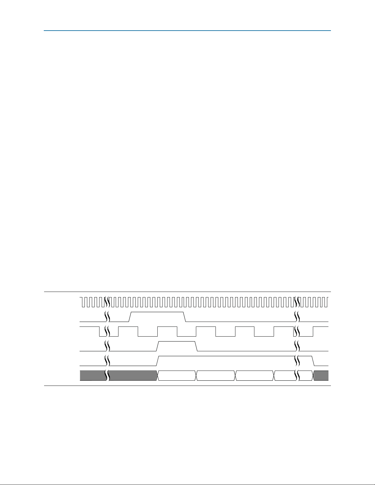
Chapter 4: Functional Description 4–27
MAP Interface
MAP Transmitter in Synchronous Buffer Mode
In the synchronized communication, called synchronous buffer mode, each AxC
interface has an incoming resynchronization signal,
software asserts this resynchronization signal synchronously with the
clock. When the application software asserts the resynchronization signal, it also
asserts the
mapN_tx_data[31:0]
mapN_tx_valid
data bus for the individual AxC interface.
signal and begins sending valid data on the
mapN_tx_resync
. Application
mapN_tx_clk
In synchronous buffer mode, the application should ignore the
signals. However, it should assert the
valid data. The CPRI IP core holds the
application must assert the
asserts the
mapN_tx_valid
mapN_tx_resync
input signals in the same cycle as the
subsequently reasserts
mapN_tx_valid
signals. However, if the application does not assert the
mapN_tx_resync
mapN_tx_valid
mapN_tx_ready
input signals when or immediately after it
while
mapN_tx_valid
transition through the MAP Tx interface buffer is lost.
1 Altera recommends that your application assert the
when it asserts the
mapN_tx_resync
signals.
For details about the behavior of the individual signals in synchronous buffer mode,
refer to “MAP Transmitter Signals” on page 6–3.
Figure 4–14 shows the expected typical behavior of the MAP Tx signals in this
synchronization mode. In this example, the CPRI line rate is 2457.6 Mbps. The
cpri_tx_start
rate determines the duration of a basic frame in
basic frame is 16
page 4–10, the
signal is asserted for the duration of a single frame, and the CPRI line
cpri_clkout
cpri_clkout
cpri_clkout
cycles. At this line rate, as shown in Table 4–2 on
frequency is 61.44 MHz. The
7.68 MHz (oversampling rate 2), approximately 0.125 times the
frequency.
mapN_tx_ready
output
input signals when sending
output signals high. The
mapN_tx_resync
signals, and
is still high, data in
mapN_tx_valid
input signals
cycles. At 2457.6 Mbps, a
mapN_tx_clk
frequency is
cpri_clkout
Figure 4–14. MAP Transmitter Interface in Synchronous Buffer Mode
cpri_clkout
cpri_tx_start
mapN_tx_clk
mapN_tx_resync
mapN_tx_valid
mapN_tx_data[31:0]
1 To ensure IP core control over the resynchronization signal timing, Altera
recommends that your application trigger the
IP core output signal
cpri_tx_start
user-programmable
December 2013 Altera Corporation CPRI MegaCore Function
cpri_tx_start
. The CPRI AUX interface asserts the
signal according to the offset value specified in the
CPRI_START_OFFSET_TX
mapN_tx_resync
register.
signal with the CPRI
User Guide
Page 60

4–28 Chapter 4: Functional Description
cpri_tx_start
cpri_tx_rfp
cpri_tx_sync_rfp
mapN_tx_resync
CPRI_START_OFFSET_TX
CPRI_MAP_OFFSET_TX
sample 0 sample 1 sample 2 sample 3 sample 4 sample 5 sample 6
sample 0 sample 1 sample 2 sample 3 sample 4 sample 5 sample 6
Write to mapN Tx buffer in the first write cycle after the resync signal:
Read from mapN Tx buffer according to CPRI_MAP_OFFSET_TX value:
MAP Interface
Asserting the resynchronization signal ensures correct alignment between the RF
implementation and the CPRI basic frame at the appropriate offset from the start of
the 10 ms radio frame. In addition to ensuring that application-specific constraints are
accommodated, the system can set the
CPRI_START_OFFSET_TX
register to an offset that
precedes the desired frame position in the CPRI transmission, in anticipation of the
delays through the antenna-carrier interface Tx buffer and out to the CPRI Tx frame
buffer. For information about these delays, refer to “Tx Path Delay” on page E–12.
Figure 4–15 shows the roles of the
CPRI_START_OFFSET_TX
and
CPRI_MAP_OFFSET_TX
registers in ensuring correct alignment.
Figure 4–15. User-Controlled Delays in Accepting Data From the AxC Data Channels in Synchronous Buffer Mode
The values programmed in the
the
cpri_tx_start
signal by the CPRI transmitter. The values in the
start_tx_offset_z, start_tx_offset_x
CPRI_START_OFFSET_TX
, and
start_tx_offset_seq
register control the assertion of
fields specify a
hyperframe number, basic frame number, and word (sequence) number in the basic
frame, respectively, within the 10 ms frame.
The system source of the AxC payload transmits the AxC container block on the data
channel to target a specific location in the 10 ms frame; the system programs the
information for this location in the
CPRI_START_OFFSET_TX
and
CPRI_MAP_OFFSET_TX
registers. The CPRI transmitter learns the location of the AxC container block on the
AxC interface from the
CPRI_START_OFFSET_TX
transmitter must assert the
CPRI_START_OFFSET_TX
register. For example, if the
register is programmed with the value 0x000595FE, the CPRI
cpri_tx_start
signal at word index 5 of basic frame 254 of
hyperframe 149 in the 10ms frame. Altera recommends that the data channel
application sample the
signal is asserted, assert the
mapN_tx_data
can begin to fill the data words at the specified position in the CPRI
frame. Assertion of the
cpri_tx_start
mapN_tx_resync
mapN_tx_resync
signal, and when it detects the
cpri_tx_start
signal to indicate that the samples on
signal resets the write pointer of the current
antenna-carrier interface (mapN) Tx buffer to zero, so that the entire buffer is
available to receive the data from the data channel. The data on
can safely be loaded in the mapN Tx buffer in the same cycle that the
mapN_tx_data[31:0]
mapN_tx_resync
signal is asserted.
CPRI MegaCore Function December 2013 Altera Corporation
User Guide
Page 61

Chapter 4: Functional Description 4–29
MAP Interface
On the CPRI side of the mapN Tx buffer, the MAP transmitter interface reads data
from the mapN Tx buffer and sends it to the CPRI transmitter interface. The offset
programmed in the
CPRI_MAP_OFFSET_TX
register tells the MAP transmitter interface
when to reset the read pointer of the mapN Tx buffer and start transferring data from
the buffer to the CPRI transmitter interface. The K counter is reset to zero at the same
time, so that it advances from zero with the transfer of the data to the CPRI
transmitter interface, tracking the packing of the AxC container block contents into
the CPRI frame.
Because the mapN Tx buffer should not be read before it is written, the offset specified
in the
CPRI_START_OFFSET_TX
CPRI_MAP_OFFSET_TX
underflow (in the
register. The CPRI IP core informs you of buffer overflow and
CPRI_IQ_TX_BUF_STATUS
page 7–22 and as reported in the
register must precede the offset specified in the
register described in Table 7–49 on
mapN_tx_status_data
output vector described in
Table 6–2 on page 6–4), but it does not prevent them from occurring. Altera
recommends that you implement a separate tracking protocol to ensure you do not
overflow or underflow the mapN Tx buffer.
In synchronous buffer mode, because programmed offsets control the mapN Tx buffer
pointers, the delay through each mapN Tx buffer can be quantified.
MAP Transmitter in the Internally-clocked Mode
In the internally-clocked mode, each data channel, or AxC interface, has an output
ready signal,
ready to receive data on this data channel for transmission to the CPRI protocol
interface—when the buffer level is at or below the threshold indicated in the
CPRI_MAP_TX_READY_THR
After the CPRI IP core asserts the
respond by asserting the
In every
present valid data on
READY_LATENCY
For details about the behavior of the individual signals in the internally-clocked
mode, refer to “MAP Transmitter Signals” on page 6–3.
mapN_tx_ready
cpri_clkout
value 1.
. Each AxC interface asserts its ready signal when it is
register.
mapN_tx_ready
mapN_tx_valid
cycle in which
mapN_tx_data
signal, the application is expected to
signal and presenting data on
mapN_tx_ready
is asserted, the application can
mapN_tx_data
, as prescribed by the Avalon-ST specification with
.
December 2013 Altera Corporation CPRI MegaCore Function
User Guide
Page 62

4–30 Chapter 4: Functional Description
Auxiliary Interface
Figure 4–16 shows an example of the behavior of the MAP Tx signals in this
synchronization mode in the basic mapping mode (
map_mode
= 2’b00).
Figure 4–16. MAP Transmitter Interface in the Internally-Clocked Mode
cpri_clkout
cpri_tx_hfn
cpri_tx_x
map0_tx_ready
map0_tx_valid
map0_tx_data[31:0]
map1_tx_ready
map1_tx_valid
map1_tx_data[31:0]
map2_tx_ready
map2_tx_valid
map2_tx_data[31:0]
3
33
4 5 67
A
B
CD EF GH
A
BC D E F
AB C D E F GH
GH
In the internally-clocked mode the delay in the AxC interface block from each data
channel can be quantified, because this delay is determined solely by the value in the
CPRI_MAP_OFFSET_TX
register.
Auxiliary Interface
The CPRI auxiliary interface enables multi-hop routing applications and provides
timing reference information for transmitted and received frames.
The auxiliary (AUX) interface allows you to connect CPRI IP core instances and other
system components together by supporting a direct connection to a user-defined
routing layer or custom mapping block. You implement this routing layer, which is
not defined in the CPRI V5.0 Specification, outside the CPRI IP core. The AUX
interface supports the transmission and reception of IQ data and timing information
between an RE slave and an RE master, allowing you to define a custom routing layer
that enables daisy-chain configurations of RE master and slave ports. Your custom
routing layer determines the IQ sample data to pass to other REs to support multi-hop
network configurations or to bypass the CPRI IP core MAP interface to implement
custom mapping algorithms outside the IP core.
CPRI MegaCore Function December 2013 Altera Corporation
User Guide
Page 63

Chapter 4: Functional Description 4–31
Auxiliary Interface
The CPRI IP core implements the AUX receiver and AUX transmitter interfaces as
separate Avalon-ST interfaces. The AUX transmitter receives data to be transmitted on
the outgoing CPRI link, and the AUX receiver transmits data received from the
incoming CPRI link.
f For information about the Avalon-ST interface, refer to Avalon Interface Specifications.
AUX Receiver Module
The AUX receiver module transmits data that the CPRI IP core received on the CPRI
link to the outgoing AUX Avalon-ST interface. In addition, it provides detailed
information about the current state in the Rx CPRI frame synchronization state
machine. This information is useful for custom user logic, including frame
synchronization across hops in multihop configurations.
The AUX interface receiver module provides the following data and synchronization
lines:
■
cpri_rx_sync_state
synchronization have been achieved in CPRI receiver frame synchronization
■
cpri_rx_start
offset defined in the
—when set, indicates that Rx, HFN, and BFN
—asserted for the duration of the first basic frame following the
CPRI_START_OFFSET_RX
register
■
cpri_rx_rfp
and
cpri_rx_hfp
—synchronization pulses for start of 10 ms radio
frame and start of hyperframe
■
cpri_rx_bfn
■
cpri_rx_x
■
cpri_rx_seq
■
cpri_rx_aux_data
and
cpri_rx_hfn
—current radio frame and hyperframe numbers
—index number of the current basic frame in the current hyperframe
—index number of the current 32-bit word in the current basic frame
—outgoing data port for sending data and control words
received on the CPRI link out on the AUX interface
The output synchronization signals are derived from the CPRI frame synchronization
state machine. These signals are all fields in the
aux_rx_status_data
bus. For
additional information about the AUX receiver signals, refer to Table 6–3 on page 6–6.
December 2013 Altera Corporation CPRI MegaCore Function
User Guide
Page 64
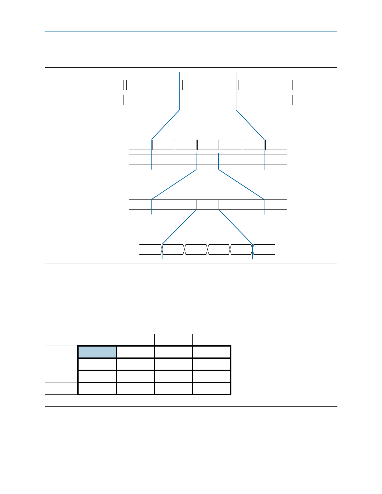
4–32 Chapter 4: Functional Description
cpri_{rx,tx}_rfp
cpri_{rx,tx}_bfn
cpri_{rx,tx}_hfp
cpri_{rx,tx}_hfn
cpri_{rx,tx}_x
cpri_{rx,tx}_seq
0 1 ... NUM_SEQ - 1
2 ...
...210
255
149
10
n n + 1 n + 2
Hyperframe
Radio Frame (10 ms)
Basic Frame
Auxiliary Interface
Figure 4–17 shows the relationship between the synchronization pulses and numbers.
Figure 4–17. Synchronization Pulses and Numbers on the AUX Interfaces
The AUX receiver presents data on the AUX interface in fixed 32-bit words. The
mapping to 32-bit words depends on the CPRI IP core line rate. Figure 4–18 shows
how the data received from the CPRI protocol interface module is mapped to the AUX
Avalon-ST 32-bit interface.
Figure 4–18. AUX Interface Data at Different CPRI Line Rates (Part 1 of 3)
614.4 Mbps
Line Rate:
0123
[31:24]:
#Z.X.0.0
[23:16]: #Z.X.1.0 #Z.X.5.0 #Z.X.9.0 #Z.X.13.0
(1)
#Z.X.4.0 #Z.X.8.0 #Z.X.12.0
Sequence number on AUX interface
[15:8]: #Z.X.2.0 #Z.X.6.0 #Z.X.10.0 #Z.X.14.0
[7:0]: #Z.X.3.0 #Z.X.7.0 #Z.X.11.0 #Z.X.15.0
CPRI MegaCore Function December 2013 Altera Corporation
User Guide
Page 65

Chapter 4: Functional Description 4–33
Auxiliary Interface
Figure 4–18. AUX Interface Data at Different CPRI Line Rates (Part 2 of 3)
1228.8 Mbps
Line Rate:
[31:24]:
[23:16]:
012 ... 7
#Z.X.0.0
#Z.X.0.1
(1)
(1)
#Z.X.2.0 #Z.X.4.0 ... #Z.X.14.0
#Z.X.2.1 #Z.X.4.1 ... #Z.X.14.1
Sequence number on AUX interface
[15:8]: #Z.X.1.0 #Z.X.3.0 #Z.X.5.0 ... #Z.X.15.0
[7:0]: #Z.X.1.1 #Z.X.3.1 #Z.X.5.1 ... #Z.X.15.1
2457.6 Mbps
Line Rate:
[31:24]:
[23:16]:
[15:8]:
[7:0]:
3072.0 Mbps
Line Rate:
[31:24]:
[23:16]:
[15:8]:
[7:0]:
012 ... 15
#Z.X.0.0
#Z.X.0.1
#Z.X.0.2
#Z.X.0.3
(1)
(1)
(1)
(1)
#Z.X.1.0 #Z.X.2.0 ... #Z.X.15.0
#Z.X.1.1 #Z.X.2.1 ... #Z.X.15.1
#Z.X.1.2 #Z.X.2.2 ... #Z.X.15.2
#Z.X.1.3 #Z.X.2.3 ... #Z.X.15.3
012 ... 1819
#Z.X.0.0
#Z.X.0.1
#Z.X.0.2
#Z.X.0.3
(1)
#Z.X.0.4
(1)
(1)
(1)
#Z.X.1.0 #Z.X.1.4 ... #Z.X.14.3 #Z.X.15.2
#Z.X.1.1 #Z.X.2.0 ... #Z.X.14.4 #Z.X.15.3
#Z.X.1.2 #Z.X.2.1 ... #Z.X.15.0 #Z.X.15.4
Sequence number on AUX interface
Sequence number on AUX interface
(1)
#Z.X.1.3 ... #Z.X.14.2 #Z.X.15.1
4915.0 Mbps
Line Rate:
[31:24]:
[23:16]:
[15:8]:
[7:0]:
December 2013 Altera Corporation CPRI MegaCore Function
012 ... 3031
#Z.X.0.0
#Z.X.0.1
#Z.X.0.2
#Z.X.0.3
(1)
#Z.X.0.4
(1)
#Z.X.0.5
(1)
#Z.X.0.6
(1)
#Z.X.0.7
(1)
(1)
(1)
(1)
Sequence number on AUX interface
#Z.X.1.0 ... #Z.X.14.0 #Z.X.15.4
#Z.X.1.1 ... #Z.X.14.1 #Z.X.15.5
#Z.X.2.2 ... #Z.X.14.2 #Z.X.15.6
#Z.X.2.3 ... #Z.X.15.3 #Z.X.15.7
User Guide
Page 66

4–34 Chapter 4: Functional Description
Auxiliary Interface
Figure 4–18. AUX Interface Data at Different CPRI Line Rates (Part 3 of 3)
6144.0 Mbps
Line Rate:
[31:24]:
[23:16]:
[15:8]:
[7:0]:
012 ... 3839
#Z.X.0.0
#Z.X.0.1
#Z.X.0.2
#Z.X.0.3
(1)
#Z.X.0.4
(1)
#Z.X.0.5
(1)
#Z.X.0.6
(1)
#Z.X.0.7
(1)
(1)
(1)
(1)
9830.4 Mbps
Line Rate:
[31:24]:
[23:16]:
[15:8]:
[7:0]:
Note to Figure 4–18:
(1) Light blue table cells indicate control word bytes. White table cells indicate data word bytes.
0 1 2 3 ... 62 63
#Z.X.0.0
#Z.X.0.1
#Z.X.0.2
#Z.X.0.3
(1)
#Z.X.0.4
(1)
#Z.X.0.5
(1)
#Z.X.0.6
(1)
#Z.X.0.7
(1)
(1)
(1)
(1)
Sequence number on AUX interface
#Z.X.0.8
#Z.X.0.9
(1)
(1)
... #Z.X.15.2 #Z.X.15.6
... #Z.X.15.3 #Z.X.15.7
#Z.X.1.0 ... #Z.X.15.4 #Z.X.15.8
#Z.X.1.1 ... #Z.X.15.5 #Z.X.15.9
Sequence number on AUX interface
#Z.X.0.8
#Z.X.0.9
#Z.X.0.10
#Z.X.0.11
(1)
(1)
(1)
(1)
#Z.X.0.12
#Z.X.0.13
#Z.X.0.14
#Z.X.0.15
(1)
(1)
(1)
(1)
... #Z.X.15.8 #Z.X.15.12
... #Z.X.15.9 #Z.X.15.13
... #Z.X.15.10 #Z.X.15.14
... #Z.X.15.11 #Z.X.15.15
AUX Transmitter Module
The AUX transmitter module receives data on the incoming AUX Avalon-ST interface
and sends it to the CPRI IP core physical layer to transmit on the CPRI link. In
addition, it outputs CPRI link frame synchronization information, to enable
synchronization of the AUX data.
CPRI MegaCore Function December 2013 Altera Corporation
User Guide
Page 67

Chapter 4: Functional Description 4–35
cpri_tx_seq[5:0]
internal tx_seq value[5:0]
CPRI Frame
210 3 4
3938
3638
Ctrl Ctrl {Ctrl,feed}
0 1 2
37 3839
cpri_tx_aux_mask[31:0]
cpri_tx_aux_data[31:0]
(1)
(1)
00000000 00000000 00000000 ffffffff ffffffff0000ffff
00000000 00000000
00000000
00000000 00000000 0000feed
2 cpri_clkout cycles
Auxiliary Interface
The incoming data on the AUX interface must match the CPRI frame with a delay of
exactly two
the AUX Tx interface is two
cpri_clkout
clock cycles. The
cpri_clkout
cpri_tx_seq[5:0]
value that you read at
cycles ahead of the internal sequence
number that tracks the CPRI frame. If you want your IQ sample to land at sequence
number N of the CPRI frame, then you must present your sample at the AUX Tx
interface when
cpri_tx_seq[5:0]
has the value of N+2. Figure 4–19 shows the
expected timing on the incoming AUX connection in a variation with a CPRI line rate
of 6144.4 Mbps.
Figure 4–19. Incoming AUX Link Synchronization
Note to Figure 4–19:
(1) The
cpri_tx_aux_data
and
cpri_tx_aux_mask
In Figure 4–19, the application presents data when
4, and sets the value of
signals are fields in the
cpri_tx_aux_mask
aux_tx_mask_data
input bus. Refer to Table 6–4 on page 6–7.
cpri_tx_seq[5:0]
has the value of
, to ensure the data is loaded in the CPRI
frame immediately following the control word. Because the CPRI line rate in this
example is 6144.4 Mbps, the length of the control word is ten bytes. Therefore, the
application presents the data when
cpri_tx_seq[5:0]
has the value of 4 to ensure the
data is loaded in the CPRI frame at position 2.
In addition, to ensure the CPRI IP core transmits the incoming AUX data correctly on
the CPRI link, you must format the incoming AUX data in the correct order to match
the CPRI IP core internal data representation. If you connect two Altera CPRI IP cores
through a routing layer, and your routing layer does not modify the data transmission
order, then the correct order is guaranteed. However, if a different application
transmits data to the CPRI IP core AUX interface, it must enforce the data order that
the CPRI IP core expects.
Incoming AUX data to the CPRI IP core appears on
called
aux_tx_mask_data[64:32]
[7:0] (39:32]) is transmitted last:
. Byte [31:24] (64:56]) is transmitted first, and byte
cpri_tx_aux_data[31:24]
cpri_tx_aux_data[31:0]
is byte 0 in the
, also
transmission order, and contains the least significant I- and Q-nibbles of the data
sample. Figure 4–20 illustrates the required data order on this data bus.
Figure 4–20. Required Data Sample Order in aux_tx_mask_data[63:32] (cpri_tx_aux_data[31:0])
63 56 55 48 47 40 39 32
I[10]
Q[10]
I[9]
Q[9]
I[8]
Q[8]
I[15]
Q[15]
I[14]
Q[14]
I[13]
Q[13]
I[12]
User Guide
I[3]
Q[3]
I[2]
Q[2]
I[1]
December 2013 Altera Corporation CPRI MegaCore Function
Q[1]
I[0]
Q[0]
I[7]
Q[7]
I[6]
Q[6]
I[5]
Q[5]
I[4]
Q[4]
I[11]
Q[11]
Q[12]
Page 68

4–36 Chapter 4: Functional Description
Auxiliary Interface
The CPRI IP core passes the incoming AUX data through to the CPRI link
unmodified. You must ensure that the incoming AUX data bits already include any
CRC values expected by the application at the other end of the CPRI link.
The CPRI transmitter frame synchronization state machine provides the following
data and synchronization signals on the AUX interface to enable the required precise
frame timing:
■
cpri_tx_start
offset defined in the
■
cpri_tx_rfp
—asserted for the duration of the first basic frame following the
and
cpri_tx_hfp
CPRI_START_OFFSET_TX
—synchronization pulses for start of 10 ms radio
register
frame and start of hyperframe
■
cpri_tx_bfn
■
cpri_tx_x
■
cpri_tx_seq
■
cpri_tx_aux_data
■
cpri_tx_aux_mask
and
cpri_tx_hfn
—current radio frame and hyperframe numbers
—index number of the current basic frame in the current hyperframe
—index number of the current 32-bit word in the current basic frame
—incoming data port for data on the AUX link
—incoming bit mask for AUX link data that indicates bits that
must be transmitted without changes to the CPRI link
The CPRI IP core layer 1 uses the
cpri_tx_aux_mask
to select the enabled bit
values in the control transmit table. When mask bits are set, the corresponding
data bits from the AUX interface fill the CPRI frame, overriding any
internally-generated information. You must deassert all the mask bits during
K28.5 character insertion in the outgoing CPRI frame (which occurs when Z=X=0).
Otherwise, the CPRI IP core asserts an error signal
following
cpri_clkout
clock cycle to indicate that the K28.5 character expected by
cpri_tx_error
on the
the CPRI link protocol has been overwritten. You must also ensure you do not
override synchronization counter values in the control word.
The AUX transmitter module also receives a synchronization pulse in an REC master.
Application software can pulse the
cpri_tx_sync_rfp
input signal to resynchronize
the 10 ms radio frame. Asserting this signal resets the frame synchronization machine
in an REC master.
In response to the rising edge of its
(
aux_tx_mask_data[64]
The rising edge of the
cpri_clkout
pulse, the
cpri_tx_hfn
clock. On the seventh
cpri_tx_hfp
signals have the value 0, and the
), a CPRI REC master IP core restarts the 10 ms radio frame.
cpri_tx_sync_rfp
and
cpri_tx_rfp
cpri_tx_sync_rfp
input signal
signal must be synchronous with the
cpri_clkout
signals pulse, the
cycle following a
cpri_tx_x
cpri_tx_bfn
signal increments from its
cpri_tx_sync_rfp
and
CPRI MegaCore Function December 2013 Altera Corporation
User Guide
Page 69

Chapter 4: Functional Description 4–37
cpri_clkout
cpri_tx_sync_rfp
cpri_tx_seq
cpri_tx_x
cpri_tx_hfn
cpri_tx_bfn
cpri_tx_hfp
cpri_tx_start
cpri_tx_rfp
5 6 7 0 1 2 3 4 5 6 7 8 9 10 0 1 2 3 4 5 6
3 4 0
3
0
2
3
Media Independent Interface to an External Ethernet Block
previous value. Figure 4–21 illustrates the behavior of the CPRI IP core signals in
response to the
cpri_tx_sync_rfp
pulse.
Figure 4–21. CPRI REC Master Response to cpri_tx_sync_rfp Resynchronization Pulse
For more information about the relationships between the synchronization pulses and
numbers, refer to Figure 4–17 on page 4–32. For the mapping of data between the
AUX interface and the CPRI link, refer to Figure 4–18 on page 4–32.
The
cpri_tx_aux_data
aux_tx_mask_data
the
aux_tx_status_data
and
cpri_tx_aux_mask
signals are fields of the
bus. The other signals described in the preceding list are fields of
bus. For additional information about the AUX transmitter
signals, refer to Table 6–4 on page 6–7.
Media Independent Interface to an External Ethernet Block
The media independent (MI) interface, or MII, allows the CPRI IP core to
communicate directly with an external Ethernet MAC block, replacing the internal
Ethernet MAC. You specify in the CPRI parameter editor whether to implement this
interface or to use the Ethernet MAC block available with the CPRI IP core. The two
options are mutually exclusive.
If you configure the CPRI IP core with the MII, you must implement the Ethernet
MAC block outside the CPRI IP core.
The MI interface is not a true media-independent interface, because it is clocked by
the
cpri_clkout
signals directly), whose frequencies do not match the usual 2.5 MHz and 25 MHz
frequencies of the media-independent protocol specification. If you use this interface,
your external Ethernet block must communicate with the CPRI IP core synchronously
with the
cpri_mii_txclk
The MII supports the bandwidth described in the CPRI V5.0 Specification in Table 12,
Achievable Ethernet bit rates.
clock (which drives the
and
cpri_mii_rxclk
cpri_mii_txclk
clocks.
and
cpri_mii_rxclk
clock
December 2013 Altera Corporation CPRI MegaCore Function
User Guide
Page 70

4–38 Chapter 4: Functional Description
Media Independent Interface to an External Ethernet Block
MII Transmitter
The MII transmitter module receives data from the external Ethernet MAC block and
writes it to the CPRI transmitter module, which transmits it on the CPRI link. It
performs 4B/5B encoding on the incoming data nibbles before sending them to the
CPRI transmitter module.
After the CPRI IP core achieves frame synchronization, the MII transmitter module
can accept incoming data on the MII. The MII transmitter module asserts the
cpri_mii_txrd
MAC block. After the
asserts the
transmitter module deasserts the
cycle in which it receives data. It may remain deasserted for multiple cycles, to
prevent buffer overflow. While the
Ethernet block must maintain the data value on
signal to indicate it is ready to accept data from the external Ethernet
cpri_mii_txrd
cpri_mii_txen
signal to indicate it is ready to provide data. The MII
signal is asserted, the external Ethernet block
cpri_mii_txrd
cpri_mii_txrd
signal in the cycle following each
signal remains low, the external
cpri_mii_txd
.
During the first
cpri_mii_txclk
cycle in which
cpri_mii_txen
is asserted, the MII
module inserts an Ethernet J symbol (5’b11000) in the buffer of data to be transmitted
to the CPRI link; during the second cycle in which
cpri_mii_txen
is asserted, the MII
module inserts an Ethernet K symbol (5’b10001) in this buffer. These two symbols
indicate Ethernet start-of-packet. While the CPRI MII transmitter is inserting the J and
K symbols, it ignores incoming data on
Typically, the external Ethernet block asserts
cpri_mii_txrd
is asserted. While the
transmitter module reads data on the
data sequence, in the first two
cpri_mii_txclk
cpri_mii_txd
cpri_mii_txen
cpri_mii_txen
cpri_mii_txd
cycles in which the
. Refer to Figure 4–22.
one clock cycle after
signal remains asserted, the MII
input data bus. Following this
cpri_mii_txen
signal is not asserted, the MII module inserts an Ethernet end-of-packet symbol—T
followed by R. While the CPRI MII transmitter is inserting the T and R symbols, it
ignores incoming data on
While
cpri_mii_txen
current nibble on
observes that both
cpri_mii_txclk
cpri_mii_txd
cpri_mii_txen
cycle, the MII module inserts an Ethernet HALT symbol (5’b00100).
Figure 4–24 on page 4–41 provides an example in which the
cpri_mii_txd
is asserted, the
is suspect. Therefore, if the MII transmitter module
and
. Refer to Figure 4–22.
cpri_mii_txer
cpri_mii_txer
input signal indicates that the
are asserted in the same
cpri_mii_txer
signal is
asserted, and shows how the error indication propagates to the MII receiver module
on the CPRI link slave.
CPRI MegaCore Function December 2013 Altera Corporation
User Guide
Page 71

Chapter 4: Functional Description 4–39
Media Independent Interface to an External Ethernet Block
Figure 4–22 illustrates the MII transmitter protocol with no input errors. The
cpri_mii_txen
Although
an Ethernet packet on
transmitter can deassert
signal remains asserted for the duration of the packet transfer.
cpri_mii_txrd
can be reasserted every other cycle during transmission of
cpri_mii_txd
cpri_mii_txrd
, this need not always occur. The CPRI MII
for more than one cycle to backpressure the
external Ethernet block. In that case, the external Ethernet block must maintain the
data value on
cpri_mii_txd
until the cycle following reassertion of
cpri_mii_txrd
.
Figure 4–22. CPRI MII Transmitter Example
cpri_mii_txclk
cpri_mii_txrd
cpri_mii_txen
cpri_mii_txd[3:0]
cpri_mii_txer
decoded result
(conceptual)
txen is asserted
>1 cycle
after
txrd assertion
cpri_mii_txen
If
>1 cycle
without
txen response
> IDLEs
txen asserted
2 cycles in which
txrd is asserted
Idle J K D0D0D1D1D2D2D3
to backpressure the Ethernet block
is deasserted while
txrd is deasserted
an additional cycle
Ethernet packet
cpri_mii_txrd
reasserted in the cycle following the reassertion of
D3
D4
D4
is deasserted, and is not
cpri_mii_txrd
No txen response
to 2 cycles
in which
txrd asserted
D5
D5 T R Idle
, then the CPRI MII
txrd asserted
transmitter inserts a T symbol in the packet; therefore, the external Ethernet block
must reassert
during transmission of an Ethernet packet on
cpri_mii_txen
in the cycle following reassertion of
cpri_mii_txd
.
cpri_mii_txrd
For more information about the MII transmitter module, refer to “CPRI MII
Transmitter Signals” on page 6–10.
,
MII Receiver
The MII receiver module receives data from the CPRI link by reading it from the CPRI
receiver module. It performs 4B/5B decoding on the 5-bit data values before
transmitting them as 4-bit data values on the MII.
After the CPRI IP core achieves frame synchronization, the MII receiver module can
send data to the external Ethernet block. The MII receiver module transmits the K
nibble to indicate start-of-frame on the MII. The J nibble of the start-of-frame is
consumed by the CPRI IP core, and is not transmitted on the MII.
December 2013 Altera Corporation CPRI MegaCore Function
User Guide
Page 72

4–40 Chapter 4: Functional Description
Media Independent Interface to an External Ethernet Block
The MII receiver module transmits the K nibble and then the data to the
output data bus and asserts the
currently on
cpri_mii_rxd
cpri_mii_rxd
the first
cpri_mii_rxclk
receiver module asserts the
completes sending data to the external Ethernet block, it deasserts the
signal.
While frame synchronization is not achieved, the
asserted and
cpri_mii_rxdv
Figure 4–23 illustrates the MII receiver protocol.
Figure 4–23. CPRI MII Receiver Example
cpri_mii_rxclk
cpri_mii_rxwr
cpri_mii_rxdv
cpri_mii_rxd[3:0]
reset
cpri_mii_rxdv
signal to indicate that the data
is valid. It sends the K nibble and the data to the
output data bus on the rising edge of the
cycle of every new data value on
cpri_mii_rxwr
signal. After the MII receiver module
cpri_mii_rxer
remains deasserted.
D0 D1K D2 D3 D4 D5 D6 D7
cpri_mii_rxclk
cpri_mii_rxd
cpri_mii_rxdv
signal remains
cpri_mii_rxd
clock. During
, the MII
cpri_mii_rxer
Frame Synchronization
Achieved
CPRI MegaCore Function December 2013 Altera Corporation
User Guide
Page 73

Chapter 4: Functional Description 4–41
cpri_mii_txclk
cpri_mii_txrd
cpri_mii_txen
cpri_mii_txd[3:0]
cpri_mii_txer
cpri_mii_rxclk
cpri_mii_rxwr
cpri_mii_rxdv
cpri_mii_rxd[3:0]
D0 D1 D2 D3 D4 D5 D6 D7
D0
K
D1 D2 D3 F D5 D6 D7
cpri_mii_rxer
CPU Interface
Figure 4–24 shows an example timing diagram in which an input error is noted on the
MII of a transmitting RE or REC master, and the data from the MII is transmitted on
the CPRI link to a receiving RE slave. The timing diagram shows the MII signals on
the transmitting master and the receiving slave. The data value captured on the MII
transmitter module of the RE or REC master when
cpri_mii_txer
is asserted, is
passed to the CPRI link as a 5-bit Ethernet HALT symbol (5’b00100). The RE slave MII
receiver module decodes this symbol as an F (4’b1111) while the
cpri_mii_rxer
signal
is asserted.
Figure 4–24. CPRI MII Signals on Transmitting RE or REC Master and on Receiving RE Slave
For more information about the MII receiver module, refer to “CPRI MII Receiver
Signals” on page 6–10.
CPU Interface
Use the CPU interface to communicate the contents of the control word of a CPRI
hyperframe — VSS, Ethernet, High-Level Data Link Controller (HDLC), and
synchronization and timing information — and to access status and configuration
information in the CPRI IP core registers. An on-chip processor such as the Nios II
processor, or an external processor, can access the CPRI configuration address space
using this interface.
The CPU interface provides an Avalon-MM slave interface that accesses all registers in
f For information about the Avalon-MM interface, refer to Avalon Interface Specifications.
December 2013 Altera Corporation CPRI MegaCore Function
the CPRI IP core. The Avalon-MM slave executes transfers between the CPRI IP core
and the user-defined logic in your design.
User Guide
Page 74

4–42 Chapter 4: Functional Description
CPU Interface
Each of the three sources of input to the CPU interface communicates with the CPRI
IP core by reading and writing registers through a single Avalon-MM port on the CPU
interface. Arbitration among the different sources must occur outside the CPRI IP
core.
If the CPRI IP core is configured with an MII, the application cannot access the IP
core’s Ethernet registers through the CPU interface. However, if the HDLC block is
configured, you can access the IP core’s HDLC registers whether or not the MII is
configured.
For more information about the CPRI IP core registers, refer to Chapter 7, Software
Interface.
Accessing the Hyperframe Control Words
When you turn on the Include Vendor Specific Space (VSS) access through CPU
interface option, you can access the 256 control words in a hyperframe through the
CPRI IP core CPU interface. The
and the
CPRI_RX_CTRL
register (Table 7–8 on page 7–6) support your application in
reading the incoming control words, and the
page 7–4),
CPRI_CTRL_INDEX
page 7–6) support the application in writing to outgoing control words.
CPRI_CTRL_INDEX
register, and
register (Table 7–7 on page 7–5)
CPRI_CONFIG
CPRI_TX_CTRL
register (Ta bl e 7 –6 on
register (Table 7–9 on
Register support provides you access to the full control word. Alternatively, in
timing-critical applications, you can access the full control words through the CPRI IP
core AUX interface.
1 Altera recommends that you use the CPU interface to access the hyperframe control
words only in applications that are not timing-critical.
CPRI MegaCore Function December 2013 Altera Corporation
User Guide
Page 75

Chapter 4: Functional Description 4–43
CPU Interface
Tab le 4– 13 summarizes the relevant register fields. For complete information, refer to
the register tables in Chapter 7, Software Interface.
Table 4–13. Register Support for Control Word Access
Register
CPRI_CTRL_INDEX
(Table 7–7)
CPRI_RX_CTRL
(Table 7–8
CPRI_TX_CTRL
(Table 7–9
CPRI_CONFIG
(Table 7–6
)
)
)
Register
Bits
[16]
[9:8]
[7:0]
[31:0]
[31:0]
[0]
Field Name Description
Control word 32-bit section transmit enable. This value is stored
in the control transmit table with its associated entry. When you
tx_control_insert
cpri_ctrl_position
cpri_ctrl_index
rx_control_data
tx_control_data
tx_ctrl_insert_en
change the value of the
tx_control_insert
appears in the
At the time the CPRI IP core can insert a control transmit table
entry in the associated position in the outgoing hyperframe on
the CPRI link, if the
that entry has the value of 1, and the
of the
CPRI_CONFIG
table entry in the hyperframe.
Sequence number for CPRI control word 32-bit section
monitoring and insertion. The value in this field determines the
32-bit section of the control receive and control transmit table
entries that appear in the
registers.
Index for CPRI control word monitoring and insertion. The value
in this field determines the control receive and control transmit
table entries that appear in the
CPRI_TX_CTRL
Most recent received CPRI control word 32-bit section from
CPRI hyperframe position Z.x, where x is the index in the
cpri_ctrl_index
cpri_ctrl_position
indicates whether this is the first, second, third, or fourth such
32-bit section.
32-bit section of CPRI control word to be transmitted in CPRI
hyperframe position Z.x, where x is the index in the
cpri_ctrl_index
cpri_ctrl_position
indicates whether this is the first, second, third, or fourth such
32-bit section.
Master enable for insertion of control transmit table entries in
CPRI hyperframe. This signal enables control words for which
the
tx_control_insert
frame.
tx_control_insert
registers.
cpri_ctrl_index
value associated with the indexed entry
tx_control_insert
register is asserted, the IP core inserts the
field of the
field of the
field of the
field of the
field, the stored
field.
bit associated with
tx_ctrl_insert_en
CPRI_RX_CTRL
CPRI_RX_CTRL
CPRI_CTRL_INDEX
CPRI_CTRL_INDEX
bit is high to be written to the CPRI
and
CPRI_TX_CTRL
and
register. The
CPRI_CTRL_INDEX
register. The
CPRI_CTRL_INDEX
bit
register
register
Recording and Retrieving the Incoming Control Words
A control receive table contains one entry for each of the 256 control words in the
current hyperframe. To read a control word, your application must write the control
word number X to the
then read the last received #Z.X control word from the
the register can hold only 32 bits at a time, depending on the CPRI line rate, reading
the full control word may require multiple register accesses. Increment the value in
the
cpri_ctrl_position
December 2013 Altera Corporation CPRI MegaCore Function
cpri_ctrl_index
field of the
CPRI_CTRL_INDEX
field of the
CPRI_CTRL_INDEX
CPRI_RX_CTRL
register and
register. Because
register from zero to three to
User Guide
Page 76

4–44 Chapter 4: Functional Description
CPU Interface
access the full control word when the CPRI line rate is 9.8304 Gbps, or from zero to
two when the CPRI line rate is 6.144 Gbps, for example. Refer to “Control Word
Retrieval Example” on page 4–47 for an example.
Tab le 4– 14 shows the positions of the control word bytes in
control word nibble appears in the table as 0xF. For example, at the CPRI line rate of
614.4 Mbps, when you access control receive table entry X by reading from the
CPRI_RX_CTRL
register, the 8-bit control word from hyperframe position #Z.X.0 is in
bits [31:24] of the register. At the CPRI line rate of 1228.8 Mbps, the byte from position
#Z.X.0.0 is in bits [31:24] of the register, and the byte from position #Z.X.0.1 is in bits
[23:16] of the register. At the CPRI line rate of 3072.0 Mbps, when you access a control
receive table entry by reading from the
the first read, you access the 32 bits of the control word from positions #Z.X.0.0 (in
register bits [31:24]), #Z.X.0.1 (in register bits [23:16], #Z.X.0.2 (in register bits [15:8]),
and #Z.X.0.3 (in register bits [7:0]). In the second read, you access the eight bits of the
control word from position #Z.X.0.4 in bits [31:24] of the register.
Table 4–14. Control Word Byte Positions in CPRI_RX_CTRL Register
cpri_ctrl_position
614.4 1228.8 2457.6 3072.0 4915.2 6144.0 9830.4
0 FF000000 FFFF0000 FFFFFFFF FFFFFFFF FFFFFFFF FFFFFFFF FFFFFFFF
1 0 0 0 FF000000 FFFFFFFF FFFFFFFF FFFFFFFF
2 00000FFFF0000 FFFFFFFF
3 000000FFFFFFFF
CPRI Line Rate (Mbps)
Writing the Outgoing Control Words
A control transmit table contains an entry for each of the 256 control words in the
current hyperframe. Each control transmit table entry contains a control word and an
enable bit. As the frame is created, if a control word entry is enabled, and the global
tx_ctrl_insert_en
writes the appropriate control transmit table entry to the CPRI frame’s control word.
bit in the
CPRI_CONFIG
CPRI_RX_CTRL[31:0]
CPRI_RX_CTRL
register, you must read twice. In
register is set, the low-level transmitter
. Each
You write to a control transmit table entry through the
CPRI_TX_CTRL
register. This
register access method requires that you write the control word in 32-bit sections. Use
the
cpri_ctrl_position
section you are currently writing to the
the
CPRI_TX_CTRL
register as well as the
control word byte location in the
cpri_ctrl_position
field of the
field.
CPRI_CTRL_INDEX
CPRI_TX_CTRL
CPRI_RX_CTRL
CPRI_TX_CTRL
register to specify the 32-bit
register. Table 4–14 applies to
register. Refer to Table 4–14 for
register and how to use the
To write a control word in the control transmit table, perform the following steps:
1. Write the control word number X to the
CPRI_CTRL_INDEX
2. Reset the
cpri_ctrl_position
register.
field of the
cpri_ctrl_index
CPRI_CTRL_INDEX
field of the
register to the value of
zero.
3. Write the first 32-bit section of the next intended #Z.X control word to the
CPRI_TX_CTRL
CPRI MegaCore Function December 2013 Altera Corporation
User Guide
register, as shown in Table 4–14.
Page 77

Chapter 4: Functional Description 4–45
CPU Interface
4. If the CPRI line rate is greater than 2.4576 Gbps, increment the
cpri_ctrl_position
field of the
CPRI_CTRL_INDEX
register to the value of 1 and
write the second 32-bit section of the next intended #Z.X control word to the
CPRI_TX_CTRL
register.
5. If the CPRI line rate is greater than 4.9152 Gbps, increment the
cpri_ctrl_position
field of the
CPRI_CTRL_INDEX
register to the value of 2 and
write the third 32-bit section of the next intended #Z.X control word to the
CPRI_TX_CTRL
register.
6. If the CPRI line rate is 9.8304 Gbps, increment the
CPRI_CTRL_INDEX
next intended #Z.X control word to the
7. Set the
tx_control_insert
register to the value of 3 and write the fourth 32-bit section of the
CPRI_TX_CTRL
bit in the
CPRI_CTRL_INDEX
8. After you update the control transmit table, set the
CPRI_CONFIG
register to enable the CPRI IP core to write the values from the
cpri_ctrl_position
field of the
register.
register to the value of one.
tx_ctrl_insert_en
bit of the
control transmit table to the control words in the outgoing CPRI frame.
The
tx_control_insert
bit of the
CPRI_CTRL_INDEX
register enables or disables the
transmission of the corresponding control transmit table entry in the CPRI frame. The
tx_ctrl_insert_en
the CPRI IP core writes all table entries with the
bit of the
CPRI_CONFIG
register is the master enable: when it is set,
tx_control_insert
bit set into the
CPRI frame.
December 2013 Altera Corporation CPRI MegaCore Function
User Guide
Page 78

4–46 Chapter 4: Functional Description
CPU Interface
Control Word Order
The entries in the control receive and control transmit tables match the organization of
control words in subchannels from the CPRI specification. Figure 4–25 shows this
word order. The figure is Figure 15 of the CPRI V5.0 Specification.
Figure 4–25. Illustration of Subchannels in a Hyperframe
Xs == 0 1 2 3
Ns == 0
1
2
3
4 4: Ctrl_AxC ... ... ...
7 7: Ctrl_AxC 71: Ctrl_AxC 135: Ctrl_AxC 199: Ctrl_AxC
14
15 15: Reserved 79: Reserved 143: Reserved 207: Reserved
16
19
20
Pointer P --->
62
0: K28.5 Synchronization and Timing
1: HDLC link 65: HDLC 129: HDLC 193: HDLC
2: L1 In-band 66: L1 in-band 130: L1 in-band 194: P (20 = 0x14)
3: Reserved 67: Reserved
...
...
14: Reserved
Vendor-specific
...
20: Ethernet
...
62 126 190 254
63
63 127 191 255
Figure 4–25 illustrates how the 256 control words in the hyperframe are organized as
64 subchannels of four control words each. The figure illustrates why the index X of a
control word is Ns + 64 × Xs, where Ns is the subchannel index and Xs is the index of
the control word within the subchannel.
Control Word Transmission Example
To write to the vendor-specific portion of the control word in a transmitted
hyperframe, perform the following steps:
1. Identify the indices for the vendor-specific portion of the transmit control table,
using the formula X = Ns + 64 × Xs.
In the example, Ns = 16 and Xs = 0,1,2, and 3. Therefore, the indices to be written
are 16, 80, 144, and 208.
2. For each value X in 16, 80, 144, and 208, perform the sequence of steps listed in
“Writing the Outgoing Control Words” on page 4–44.
CPRI MegaCore Function December 2013 Altera Corporation
User Guide
Page 79

Chapter 4: Functional Description 4–47
CPU Interface
After you update the control transmit table with the control bytes, to insert the data in
the next outgoing CPRI frame, make sure you set the
CPRI_CONFIG
register to the value of 1 as specified in the instructions.
tx_ctrl_insert_en
field of the
Control Word Retrieval Example
To retrieve the vendor-specific portion of a control word in the most recent received
hyperframe, perform the following steps:
1. Identify the indices for the vendor-specific portion of the transmit control table,
using the formula X = Ns + 64 × Xs.
In the example, Ns = 16 and Xs = 0,1,2, and 3. Therefore, the indices to be read are
16, 80, 144, and 208.
2. For each value X in 16, 80, 144, and 208, perform the following steps:
a. Write the value X to the
b. Reset the
cpri_ctrl_position
value of zero.
c. In the following
in the
CPRI_RX_CTRL
cpu_clk
register, as shown in Table 4–14.
d. If the CPRI line rate is greater than 2.4576 Gbps, increment the
cpri_ctrl_position
in the following
word in the
CPRI_RX_CTRL
field of the
cpu_clk
e. If the CPRI line rate is greater than 4.9152 Gbps, increment the
cpri_ctrl_position
in the following
in the
CPRI_RX_CTRL
field of the
cpu_clk
register.
f. If the CPRI line rate is 9.8304 Gbps, increment the
the
CPRI_CTRL_INDEX
register to the value of 3 and in the following
cycle, read the fourth 32-bit section of the control word in the
register.
Accessing the Ethernet Channel
If you turn on the Include MAC block parameter, your CPRI IP core includes an
internal Ethernet Media Access Controller (MAC). If you turn off this parameter, an
MII is available for you to connect to your own external Ethernet MAC. In that case,
the internal Ethernet MAC is not available and your application cannot access the
Ethernet registers. If the internal Ethernet MAC is turned off, attempts to access these
registers read zeroes and do not write successfully, as for a reserved register address.
cpri_ctrl_index
field of the
field of the
CPRI_CTRL_INDEX
CPRI_CTRL_INDEX
register.
register to the
cycle, read the first 32-bit section of the control word
CPRI_CTRL_INDEX
register to the value of 1 and
cycle, read the second 32-bit section of the control
register.
CPRI_CTRL_INDEX
register to the value of 2 and
cycle, read the third 32-bit section of the control word
cpri_ctrl_position
CPRI_RX_CTRL
field of
cpu_clk
The Ethernet MAC is responsible for processing the Ethernet frame. The Ethernet
MAC unloads the Ethernet frame from the CPRI frame and stages it in the Ethernet
registers, where it is accessible through the CPU interface. The Ethernet MAC also
handles the flow of Ethernet data to the CPRI frame, by loading it from the Ethernet
registers into the Ethernet space in the CPRI hyperframe.
December 2013 Altera Corporation CPRI MegaCore Function
User Guide
Page 80

4–48 Chapter 4: Functional Description
CPU Interface
The CPRI specification dictates that a CPRI hyperframe that contains Ethernet data
also contain a pointer to the start of that data in control byte Z.194.0. The pointer value
0x0 indicates that no Ethernet channel is supported in the current hyperframe. A valid
pointer holds a subchannel index value between 0x14 and 0x3F, inclusive. The length
of the Ethernet data can extend beyond the end of the hyperframe; if a received
Ethernet frame exceeds 1536 bytes, the Ethernet module resets, unless the
rx_long_frame_en
bit of the
ETH_CONFIG_1
register is set.
The CPRI transmitter reads the pointer value from the
CPRI_CM_CONFIG
CPRI hyperframe. The
register and writes it in CPRI control byte Z.194.0 in the outgoing
rx_fast_cm_ptr
field of the
tx_fast_cm_ptr
CPRI_CM_STATUS
field of the
register holds the
current pointer value, determined during the software set-up sequence or by dynamic
modification, in which the same new pointer value is received in CPRI control byte
Z.194.0 four hyperframes in a row.
Software can configure the Ethernet channel by writing to the
ETH_CONFIG_1
register
through the CPRI IP core Avalon-MM CPU interface. For additional information
about this register, refer to Chapter 7, Software Interface.
Transmitting Ethernet Traffic
To transmit an Ethernet frame, the CPRI IP core must load the frame in a Tx Ethernet
buffer. Application software can direct the CPRI IP core to load the Ethernet frame in
the Tx Ethernet buffer by reading and writing the following registers:
■
ETH_CONFIG_2
CPRI IP core to automatically calculate the Frame check sequence and insert it at
the end of the frame data, by setting the
■
ETH_TX_STATUS
tx_ready_block
value of 1, you can load a 4-byte word to the Tx Ethernet buffer. If the
tx_ready_block
to the Tx Ethernet buffer without polling the
between CPU write operations.
register at offset 0x20C (Table 7–54 on page 7–25)—Configure the
crc_enable
field in bit 0 of this register.
register at offset 0x204 (Table 7–52 on page 7–24)—Poll the
and
tx_ready
fields of this register. If the
tx_ready
field has a
field has a value of 1, you can load a block of eight 4-byte entries
tx_block_ready
or
tx_ready
bits
■
ETH_TX_DATA
register at offset 0x220 (Table 7–59 on page 7–26)—Load data in this
register. To load a block of eight 4-byte entries to the Tx Ethernet buffer, you must
execute eight CPU write operations to this register.
■
ETH_TX_CONTROL
load the final word of an Ethernet frame in the
ETH_TX_DATA_WAIT
write the
register at offset 0x21C (Table 7–58 on page 7–25)—Before you
register (Table 7–60 on page 7–26)), set the
tx_length
ETH_TX_DATA
field of this register to indicate how many bytes in the final
register (or
tx_eop
field and
word are padding.
The Ethernet Tx buffer holds 64 4-byte entries, for a total of 256 bytes. When
transmitting Ethernet frames larger than the capacity of the Tx Ethernet buffer, you
must ensure you do not overflow or underflow the buffer. If the Ethernet transmitter
module writes data to the
ready, the
tx_abort
ETH_TX_DATA
bit is set in the
register when the Ethernet Tx buffer is not
ETH_TX_STATUS
register and the current Ethernet
packet is aborted. To prevent the Ethernet transmitter module from aborting a frame,
you can write the data to the
ETH_TX_DATA_WAIT
register. The
ETH_TX_DATA_WAIT
register can accept data when the Ethernet Tx buffer is not ready for new data.
CPRI MegaCore Function December 2013 Altera Corporation
User Guide
Page 81

Chapter 4: Functional Description 4–49
CPU Interface
You must write each frame’s data to the
Ethernet transmitter module ensures the correct bit order for transmission on the
CPRI link. If the
must insert the CRC in the frame data, because the Ethernet receiver module checks
CRC. In this case, you must reverse the bit order of the CRC bytes so that the most
significant byte of the CRC is transmitted first.
1 If you set the
Ethernet automatically calculates the Frame check sequence and inserts it at the end of
the Ethernet frame data in the Tx Ethernet buffer.
Software can set the
causes the
tx_abort
transmitter module can also set the
The Tx Ethernet controller reads the Tx Ethernet buffer after you set the
the
ETH_TX_CONTROL
you disable the store-and-forward feature by resetting the
ETH_FWD_CONFIG
controller also reads the Tx Ethernet buffer whenever the number of words in the Tx
Ethernet buffer is above a programmable threshold.
Interrupts
Software can enable interrupts by setting bits in the
0x208 (Table 7–53 on page 7–24). The
enable and
intr_tx_en
set, software can use the status in the
For example, using the
CPU is interrupted only when a full 32-bit packet of data is ready to transfer to the
Ethernet Tx buffer.
crc_enable
crc_enable
tx_discard
bit in the
field of the
field of the
bit in the
ETH_TX_STATUS
ETH_TX_DATA
ETH_CONFIG_2
ETH_CONFIG_2
ETH_TX_CONTROL
register to be set. The Ethernet
tx_abort
bit directly.
register continuously. The
register has the value of 0, you
register to the value of 1, the Tx
register, which in turn
tx_eop
register and write the final word in the
ETH_TX_DATA
tx_st_fwd
field of the
register. If
register at offset 0x244 (Table 7–64 on page 7–27), the Tx Ethernet
intr_en
ETH_CONFIG_1
bit is the Ethernet global interrupt
register at offset
is the Ethernet Tx interrupt enable. If both of these two bits are
ETH_TX_STATUS
tx_ready_block
bit to generate an interrupt ensures that the
register to generate interrupts.
bit of
Receiving Ethernet Traffic
The Ethernet receiver module receives Ethernet data from the CPRI link by reading it
from the Ethernet Rx buffer through an Ethernet register.
This section describes how the Ethernet receiver module performs MAC address
filtering according to the
provides status information to the CPU interface in the
allows the CPU interface to insert wait states in the Ethernet channel.
For additional information about the Ethernet receiver registers, refer to Chapter 7,
Software Interface.
MAC Address Filtering
To enable MAC address checking, set the
If the
mac_check
bit is reset to the value of zero, the Ethernet receiver accepts all
received packets.
You can enable the following three MAC address filters:
■ Unicast filtering: check that the destination MAC address is the address specified
in the
ETH_ADDR_LSB
filter is disabled.
December 2013 Altera Corporation CPRI MegaCore Function
ETH_CONFIG_1, ETH_ADDR_LSB
mac_check
and
ETH_ADDR_MSB
registers. If the
, and
ETH_ADDR_MSB
ETH_RX_STATUS
bit of the
ETH_CONFIG_1
mac_check
registers,
register, and
register.
bit is not set, this
User Guide
Page 82

4–50 Chapter 4: Functional Description
■ Multicast filtering: if the least significant bit of the first destination MAC address
byte, the group address bit, is set to 1, use the
ETH_HASH_TABLE
register to
CPU Interface
determine whether to accept this destination MAC address. Because the hash
algorithm might not filter the destination address as intended, you must
implement full address validation in software if you enable multicast filtering. To
enable multicast filtering, set the
multicast_flt_en
bit of the
ETH_CONFIG_1
register.
■ Broadcast filtering: accept all packets with destination MAC address
0xFFFFFFFFFFFF, the Ethernet broadcast address. To enable broadcast filtering, set
the
broadcast_en
bit of the
ETH_CONFIG_1
register.
Ethernet Rx Buffer Status
The CPRI IP core reports relevant Ethernet Rx buffer status to the CPU interface by
updating the following fields of the
ETH_RX_STATUS
register:
■ The
ETH_RX_STATUS rx_ready
bit indicates that at least one word of data is
available in the Ethernet Rx buffer and ready to be read.
■ The
ETH_RX_STATUS rx_eop
bit indicates that the next ready data word contains
the end-of-packet byte.
■ The
ETH_RX_STATUS rx_length
field indicates the number of valid bytes in the
end-of-packet word.
■ The
ETH_RX_STATUS rx_abort
bit indicates that the current received packet is
aborted.
■ The
ETH_RX_STATUS rx_ready_block
bit indicates that the next block of packet
data is ready to be read and does not contain the end-of-packet byte.
■ The
ETH_RX_STATUS rx_ready_end
bit indicates that the end-of-packet byte is
ready in the Ethernet Rx buffer.
Software can set the
ETH_RX_CONTROL rx_discard
bit to abort the current received
packet. The Ethernet receiver ensures that following read from the Ethernet Rx buffer
is a start-of-packet word.
Ethernet Data Transfer
The next ready data word is available in the
registers. If no Ethernet data word is ready, reading from the
ETH_RX_DATA
and
ETH_RX_DATA_WAIT
ETH_RX_DATA_WAIT
register inserts wait states in the Ethernet channel. If no Ethernet data word is ready,
reading from the
ETH_RX_DATA
register causes the
rx_abort
bit to be set. The CPU
interface receiver module reads the Ethernet packet data one word at a time from one
of these registers.
Accessing the HDLC Channel
If you turn on the Include HDLC block parameter, your CPRI IP core includes an
internal High-Level Data Link Controller (HDLC) block. If you turn off this
parameter, the internal HDLC block is not available and your application cannot
access the HDLC registers. If the internal HDLC block is turned off, attempts to access
these registers read zeroes and do not write successfully, as for a reserved register
address.
CPRI MegaCore Function December 2013 Altera Corporation
User Guide
Page 83

Chapter 4: Functional Description 4–51
CPRI Protocol Interface Layer (Physical Layer)
In the CPRI IP core, the HDLC block, or slow data link layer, passes HDLC data
between the CPU interface and the CPRI receiver and transmitter interfaces to the
CPRI link. The CPRI specification dictates that the HDLC channel rate is specified in
the three lowest bits of control byte Z.66.0. The value 3’b000 indicates that no HDLC
channel is supported in the current hyperframe. Table 4–15 shows the possible rate
configurations.
Table 4–15. HDLC Channel Bit Rates
Value in Z.66.0.0[2:0]
000 — 614.4
001 240 614.4
010 480 614.4
011 960 1228.8
100 1920 2457.6
101 2400 3072.0
110
111
Note to Tab le 4– 15:
(1) When Z.66.0.0[2:0] holds value 3’b111, the HDLC bit rate is the highest HDLC bit rate possible for the current CPRI
line rate. You can derive that bit rate from the other entries in this table.
HDLC Bit Rate
(Kbps)
3840 4915.2
4800 6144.0
7680 9830.4
Minimum CPRI Line Rate
(Mbps)
(1)
The HDLC channel rate is determined during the software set-up sequence or by
dynamic modification, in which the same new pointer value is received in CPRI
control byte Z.66.0 four hyperframes in a row. The accepted receive rate is specified in
rx_slow_cm_rate
the
specified in the
field of the
tx_slow_cm_rate
CPRI_CM_STATUS
field of the
CPRI_CM_CONFIG
register, and the transmit rate is
register.
The CPU interface control for the HDLC channel is identical to the CPU interface
control for the Ethernet channel, with the following exceptions:
■ HDLC register names replace
■ HDLC channel control has fewer configurations than the Ethernet channel control
■ HDLC channel control does not support address filtering
ETH
with
HDLC
1 The CPRI IP core implements the CRCDT CRC-16 allowed by the HDLC specification,
rather than the CRC-32.
CPRI Protocol Interface Layer (Physical Layer)
The physical layer of the CPRI protocol is also called layer 1. This layer controls the
electrical characteristics of the CPRI link, the time-division multiplexing of the
separate information flows in the protocol, and low-level signaling. The CPRI
protocol interface module of the CPRI IP core incorporates Altera’s high-speed
transceivers to implement layer 1. The transceivers are configured in deterministic
latency mode, supporting the extended delay measurement requirements of the CPRI
specification.
December 2013 Altera Corporation CPRI MegaCore Function
User Guide
Page 84

4–52 Chapter 4: Functional Description
tx_dataout
CPRI Link
rx_datain
CPRI Link
Receiver Transceiver
Rx State Machine
and
Frame Alignment
DEMUX
Payload
Timing
I/Q
Payload
RFN + HFN
Recovery
Ethernet
Decode
HDLC
Bit-Destuff
VSS/L1/
Alarms
Low-Level
Receiver
CPU IF
Module
HDLC_RXETH_RXTiming
CPRI_RX_MAPAUX I F
Module
Transmitter Transceiver
Tx State Machine
MUX
Payload Ethernet
Encode
HDLC
Bit-Destuff
VSS/L1
Low-Level
Transmitter
CPU IF
Module
HDLC_TXETH_TX
Loop
Data
CPRI_TX_MAPAUX IF
Module
I/Q
Payload
Rx
Elastic Buffer
Tx
Elastic Buffer
CPRI Protocol Interface Layer (Physical Layer)
This section describes features and blocks of the CPRI protocol interface module.
Figure 4–26 shows a high-level block diagram of this module.
Features
The physical layer has the following features:
■ Frame synchronization
■ Transmitter and receiver with the following features:
■ High-speed data serialization and deserialization
■ Clock and data recovery (receiver)
■ 8B/10B encoding and decoding
■ Frame and control word assembly and delineation
■ Error detection
■ Deterministic latency
■ Software interface (status and control registers)
Physical Layer Architecture
Figure 4–26. Physical Layer High Level Block Diagram
■ Error reporting
■ Clock decoupling
Figure 4–26 shows the architecture of the physical layer.
CPRI MegaCore Function December 2013 Altera Corporation
User Guide
Page 85

Chapter 4: Functional Description 4–53
CPRI Protocol Interface Layer (Physical Layer)
Ensuring the Physical Layer Routes Your Data as Expected
Layer 1 routes data from the MAP, Auxiliary, and CPU interfaces to the outgoing
CPRI frame, and routes data from the CPRI frame to the MAP, Auxiliary, and CPU
interfaces. To ensure the data is routed as you intend, observe the following
guidelines:
■ To configure a CPRI IP core variation that supports only the AUX interface, in the
CPRI parameter editor, set the number of antenna-carrier interfaces to the value of
0.
■ To program a subset of the configured antenna-carrier channels as active
antenna-carrier channels, set the
to the appropriate number of channels. Refer to “Number of Antenna-Carrier
Interfaces” on page 3–6. The combination of CPRI line rate, MAP interface sample
width (programmed in the
and sampling rate (programmed in the
register) restricts the number of active antenna-carrier interfaces your CPRI IP core
can support without data corruption. Refer to Table 4–5 and Table 4–6 on
page 4–17. Programming these register fields affects how your AxC samples are
packed in the data channels. You can program these register fields, and they have
the same effect on the MAP interface, whether or not your CPRI IP core variation
uses the AUX interface.
map_ac
field of the
map_15bit_mode
map_n_ac
CPRI_MAP_CNT_CONFIG
field of the
field of the
CPRI_MAP_CONFIG
CPRI_MAP_CNT_CONFIG
register
register),
Receiver
■ If your CPRI IP core variation and application support both an AUX interface and
a MAP interface, use the
aux_tx_mask_data[64:0]
cpri_tx_aux_mask
mask signal (bits [31:0] of the
bus described in Table 6–4 on page 6–7) to override the
MAP interface (data) and CPU interface (control words) write access to the CPRI
frame data per data bit. The mask signal is a MUX select. Setting a bit in the mask
ensures the corresponding data bit inserted in the outgoing CPRI frame is data
from the AUX interface. Resetting a bit in the mask ensures the corresponding bit
inserted in the outgoing CPRI frame is data from the MAP interface or control
words from the CPU interface.
■ The AUX interface routes raw data. It passes control words unexamined as if they
were data. Your application can separate the control and data words in the AUX
stream if your application requires that they be separated.
■ When the source of the data for the CPRI frame is not the AUX interface, you must
ensure you deassert the bits in
cpri_tx_aux_mask
to prevent AUX data from being
inserted in the outgoing CPRI frame.
The receiver in the low-level interface receives the input from the CPRI link, and
performs the following tasks:
■ Converts the data to the main clock domain
■ Performs CPRI frame detection
■ Separates data and control words
■ Descrambles data at 4915.2 Mbps, 6144.0, and 9830.4 Mbps CPRI line rates
(optional)
December 2013 Altera Corporation CPRI MegaCore Function
User Guide
Page 86

4–54 Chapter 4: Functional Description
■ Separates data for the MAP interface block, the AUX module, the Ethernet MAC
CPRI Protocol Interface Layer (Physical Layer)
block or the MII module, and the HDLC module.
■ Detects loss of signal (LOS), loss of frame (LOF), remote alarm indication (RAI),
and service access point (SAP) defect indication (SDI) errors
High-Speed Transceiver
The high-speed transceiver on the CPRI IP core CPRI protocol interface is configured
with the Altera ALTGX megafunction in Arria II, Cyclone IV GX, and Stratix IV GX
devices, with the Altera Deterministic Latency PHY IP core in Arria V, Cyclone V, and
Stratix V GX devices and in some variations in Stratix V GT devices, and with the
Altera Native PHY IP core in variations with a CPRI line rate of 9830.4 Mbps in
Stratix V GT devices.
The transceiver receiver implements 8B/10B decoding and the deterministic latency
protocol. The deterministic latency protocol is designed to meet the 16.276 ns
round-trip delay measurement accuracy requirements R21 and R21A of the CPRI
specification.
f For information about the high-speed transceiver blocks, refer to volume 2 of the
Arria II Device Handbook, to volume 2 of the Cyclone IV Device Handbook, or to volume 2
and volume 3 of the Stratix IV Device Handbook.
f For information about the Altera Deterministic Latency PHY IP core and the Altera
Native PHY IP core, refer to the Altera Transceiver PHY IP Core User Guide.
Rx Elastic Buffer
The low-level interface receiver converts data from the transceiver clock domain and
data width to the main CPRI IP core clock domain and data width using a
synchronization FIFO called the Rx elastic buffer. The Rx elastic buffer data output is
clocked with the
with the
rx_clkout
is 32 bits, and the
wide. For details, refer to “Clock Diagrams for the CPRI IP Core” on page 4–5.
The default depth of the Rx elastic buffer is 64 32-bit entries. For most systems, the
default Rx elastic buffer depth is adequate to handle dispersion, jitter, and wander
that can occur on the link while the system is running. However, the Receiver buffer
depth parameter is available for cases in which additional depth is required.
1 Altera recommends that you set Receiver buffer depth to 4 in CPRI RE slave
variations, specifying a depth of 16 32-bit entries.
You must realign and resynchronize the Rx elastic buffer after a dynamic CPRI line
rate change. Resynchronizing the Rx elastic buffer resets its pointers. Program the
CPRI_RX_DELAY_CTRL
cpri_clkout
clock. The Rx elastic buffer data input is synchronous
clock from the transceiver. The width of an Rx elastic buffer entry
rx_clkout
clock clocks the transceiver data, which is 8, 16, or 32 bits
register to realign and resynchronize the Rx elastic buffer.
The Rx elastic buffer adds variable delay to the Rx path through the CPRI IP core.
Refer to “Extended Rx Delay Measurement” on page E–6.
CPRI MegaCore Function December 2013 Altera Corporation
User Guide
Page 87

Chapter 4: Functional Description 4–55
CPRI Protocol Interface Layer (Physical Layer)
Descrambling
If the
tx_prot_version
page 7–12) holds the value 2, and the CPRI data rate is 4915.2 Mbps, 6144.0 Mbps, or
9830.4 Mbps, the low-level CPRI receiver may need to descramble the incoming data,
depending on the values in the
field of the
CPRI_RX_SCR_SEED
CPRI_TX_PROT_VER
register.
register (Table 7–25 on
When the
rx_scr_act_indication
field of the
CPRI_RX_SCR_SEED
register (Table 7–27
on page 7–13) is set, the low-level CPRI receiver descrambles the data words
according to the CPRI V5.0 Specification, using the seed in the
the
CPRI_RX_SCR_SEED
register. The seed value may be zero, indicating the incoming
rx_scr_seed
field of
data is not scrambled.
Frame Synchronization
During frame synchronization, LOF is set to zero. LOS—the assertion of the
signal—resets the frame synchronization state machine.
Figure 4–27 shows the frame synchronization state machine. If scrambling is
configured in the CPRI link partner (based on the value at Z.2.0 in the incoming CPRI
communication), additional actions and conditions apply on the state machine
transitions, according to the CPRI V5.0 Specification. The CPRI IP core sets the values
in the
CPRI_RX_SCR_SEED
register according to these conditions.
gxb_los
December 2013 Altera Corporation CPRI MegaCore Function
User Guide
Page 88

4–56 Chapter 4: Functional Description
XACQ1
XACQ2
XSYNC1
XSYNC2
HFNSYNC
W=X=0 and LOS=0 and
(Received K28.5 Byte when Y=0
and
Received Scrambled 0x50 Byte when Y=2..5)
W=X=0 and LOS=0 and
(Received K28.5 Byte when Y=0
and
Received Scrambled 0x50 Byte when Y=2..5)
W=X=0 and LOS=0 and
(Received K28.5 Byte when Y=0
and
Received Scrambled 0x50 Byte when Y=2..5)
Received K28.5 Byte/
Set Y:=W:=X:=0
W=X=0 and LOS=0 and
(Received K28.5 Byte when Y=0
and
Received Scrambled 0x50 Byte when Y=2..5)
LOS=1
B
B
B or
LOS=1
LOF=1
LOF=0
Power Up or Reset
B or
LOS=1
(2)
(2)
(3)
(3)
(3)
(3)
(2)
CPRI Protocol Interface Layer (Physical Layer)
Figure 4–27. CPRI Frame Synchronization Machine
(1)
Notes to Figure 4–27:
(1) If the tx_prot_version field of the CPRI_TX_PROT_VER register (Table 7–25 on page 7–12) holds the value 1, scrambling is not turned on. In this
case, the conditions when Y is in 2..5 are ignored.
(2) LOS=1 returns the state machine to the XACQ1 state. This transition has highest priority.
(3) Condition B is: Received byte not K28.5 when Y=W=X=0 or for some k in 2..5, received byte(unscrambled) not 0x50 when W=X=0 and Y=k.
CPRI MegaCore Function December 2013 Altera Corporation
User Guide
Alarm Indications
The CPRI IP core can detect and report the following alarms:
■ Loss of signal (LOS)—the CPRI IP core reports this alarm in the
CPRI_STATUS
■ Loss of frame (LOF)—the CPRI IP core reports this alarm by resetting the
field of the
CPRI_STATUS
Your application detects the following alarms by reading the last received #Z.130.0
control byte in the
■ Remote alarm indication (RAI)
■ Service access point (SAP) defect indication (SDI) errors
■ Reset requests received over the CPRI link
register at offset 0x4 (Table 7–5 on page 7–3).
register at offset 0x4 (Table 7–5 on page 7–3).
CPRI_RX_CTRL
register:
rx_los
field of the
rx_state
Page 89

Chapter 4: Functional Description 4–57
CPRI Protocol Interface Layer (Physical Layer)
The frame synchronization machine detects LOS and LOF directly. You can program
your application to detect and respond to RAI and SDI errors as appropriate. Refer to
“Accessing the Hyperframe Control Words” on page 4–42 for information about
retrieving these alarms from the hyperframe control word.
The CPRI IP core handles incoming reset requests on the CPRI link by signalling the
application to assert the reset signal to reset the IP core. The application reads the
requests using the CPU interface. The following section describes the additional
support the CPRI IP core provides to process this special command.
Reset Control Word
A CPRI IP core in master clocking mode can send a reset request through the CPRI
link and a CPRI IP core in slave clocking mode can receive a reset request through the
CPRI link. As required by the CPRI specification, the reset control information is sent
in bit 0 of the CPRI hyperframe control word Z.130.0. This reset bit communicates
both reset request and reset acknowledge.
Tab le 4– 16 lists the signals and register fields that determine the CPRI IP core’s
response to a reset request received on the CPRI link and that determine whether it
sends a reset request on the CPRI link.
Table 4–16. Conditions That Trigger a Reset Request or Enable a Reset Acknowledge on the CPRI Link
Register or Signal
Name
CPRI_HW_RESET
(Table 7–12)
hw_reset_assert
(Table 6–15)
Register Bits Field Name
[0]
[1]
[3]
—— — 1
reset_gen_en
reset_gen_force
reset_hw_en
Trigger Conditions for Sending Reset
Request (Master) or ACK (Slave)
1—
1—
01
A CPRI IP core in master mode transmits a reset request to the RE slave nodes to
which it is connected under either of the trigger conditions shown in Table 4–16. The
behavior of a CPRI IP core in slave mode that receives a reset request on the CPRI link
depends on the same enable fields in its own
CPRI_HW_RESET
register. For reset
acknowledgements, as for the original reset request conditions, if the
is asserted, the
reset_gen_en
bit is ignored.
The CPRI specification requires that the Z.130.0 reset bit must be detected by the CPRI
partner in ten consecutive hyperframes before the CPRI partner confirms the reset
request. The reset generation request is in effect while the condition that triggered the
reset request remains in effect, until the reset acknowledge control bit is detected on
the incoming CPRI link.
To abort a reset request, set or reset a register field to negate the condition. Specifically,
to abort a reset request made by asserting the
CPRI_HW_RESET
register, set the
reset_gen_en
abort a reset request made by asserting the
reset_hw_en
bit of the
CPRI_HW_RESET
register to 0.
reset_gen_force
bit of the
CPRI_HW_RESET
hw_reset_assert
bit in the
input signal, set the
reset_hw_en
bit
register to 0. To
December 2013 Altera Corporation CPRI MegaCore Function
User Guide
Page 90

4–58 Chapter 4: Functional Description
CPRI Protocol Interface Layer (Physical Layer)
To acknowledge the reset request, the CPRI transmitter must send a reset
acknowledge on the CPRI link, by setting the Z.130.0 reset bit in five consecutive
outgoing hyperframes. If one of the acknowledgement conditions in Table 4–16 holds,
the CPRI transmitter sends the reset acknowledge on the CPRI link. If the
reset_out_en
external
bit of the
hw_reset_req
CPRI_HW_RESET
register is set, the CPRI IP core asserts the
signal until the reset occurs. This signal informs the
application layer of the low-level reset request.
After it transmits the five consecutive reset acknowledge bits, the CPRI transmitter
sets the
register. If the
set the
reset_gen_done
reset_hw_en
hw_reset_assert
and
reset_gen_done_hold
bit is set and the
hw_reset_req
bits of its own
CPRI_HW_RESET
signal is asserted, you must
signal, to tell the CPRI transmitter to send a reset
acknowledge on the CPRI link.
For more information about the
page 7–6. For more information about the
Table 6–15 on page 6–17.
After reset, your software must perform link synchronization and other initialization
tasks. For information about the required initialization sequence following CPRI IP
core reset, refer to Appendix A, Initialization Sequence.
Trans mitter
The transmitter in the low-level interface transmits output to the CPRI link. This
module performs the following tasks:
■ Assembles data and control words in proper output format
■ Transmits standard frame sequence
■ Optionally scrambles the outgoing data transmission at 4915.2 Mbps,
■ Inserts the following control words in their appropriate locations in the outgoing
CPRI_HW_RESET
register, refer to Table 7–12 on
hw_reset_assert
input signal, refer to
6144.0 Mbps, and 9830.4 Mbps CPRI line rates
hyperframe:
■ Synchronization control byte (K28.5) and filler bytes (D16.2) in the
synchronization control word
■ Hyperframe number (HFN)
■ Basic frame number (BFN)
■ HDLC bit rate
■ Pointer to start of Ethernet data in current frame
■ 4B/5B-encoded fast C&M Ethernet frames
■ Bit-stuffed slow C&M HDLC frames
■ Enabled control transmit table entries
■ Converts the data to the transceiver clock domain.
When no data is available to transmit on the CPRI link, the transmitter transmits the
standard frame sequence with zeroed control words and all-zero data.
CPRI MegaCore Function December 2013 Altera Corporation
User Guide
Page 91

Chapter 4: Functional Description 4–59
CPRI Protocol Interface Layer (Physical Layer)
Scrambling
When the
page 7–12) holds the value 2, the low-level CPRI transmitter scrambles the data words
according to the CPRI V5.0 Specification, using the seed in the
the
tx_prot_version
CPRI_TX_SCR_SEED
field of the
CPRI_TX_PROT_VER
register (Table 7–26 on page 7–13).
register (Table 7–25 on
tx_scr_seed
field of
Tx Elastic Buffer
The low-level interface transmitter converts data from the main CPRI IP core clock
domain and data width to the transceiver clock domain and data width using a
synchronization FIFO called the Tx elastic buffer. The Tx elastic buffer data input is
clocked with the
tx_clkout
the data bus to the transceiver is 8, 16, or 32 bits wide, depending on the target device
family and the CPRI line rate. The CPRI IP core derives the
the Tx output clock of the transceiver, divided as necessary to support the data width
conversion to and from the 32-bit wide elastic buffers. Table 4–17 shows the data bus
widths and clock divisors for the different device families and CPRI line rates.
Table 4–17. Transceiver Datapath Width and tx_clkout Divider
cpri_clkout
clock, and the buffer data output is clocked with the
clock from the transceiver. Data in the Tx elastic buffer is 32 bits wide, and
cpri_clkout
clock from
CPRI Line Rate
(Mbps)
Device Family
(1)
Transceiver Datapath Width
(Bits)
tx_clkout Divider
614.4 All 8 4
Arria II GX, Cyclone IV GX 16 2
Greater than 614.4
Arria II GZ, Arria V,
Cyclone V, Stratix IV GX, and
32 1
Stratix V
Note to Table 4–17:
(1) Arria V GT devices that target 9.830 Gbps do not have a
the input clock
cpri_clkout
usr_clk
).
. The TX elastic buffer synchronizes between the transceiver PMA clock out and the user-derived clock
tx_clkout
divider after auto-rate negotiations.
cpri_clkout
is derived directly from
High-Speed Transceiver
The high-speed transceiver on the CPRI IP core CPRI protocol interface is configured
with the Altera ALTGX megafunction in Arria II, Cyclone IV GX, and Stratix IV GX
devices, with the Altera Deterministic Latency PHY IP core in ArriaV, Cyclone V, and
Stratix V GX devices and in some variations in Stratix V GT devices, and with the
Altera Native PHY IP core in variations with a CPRI line rate of 9830.4 Mbps in
Stratix V GT devices.
The transceiver transmitter implements 8B/10B encoding and the deterministic
latency protocol. It transforms the 16-bit parallel input data to the Arria II GX or
Cyclone IV GX transmitter, or 32-bit parallel input data to the Arria II GZ, Arria V,
Stratix IV GX, or Stratix V transmitter, to 8-bit data before 8B/10B encoding. The 10bit encoded data is then serialized and sent to the CPRI link differential output pins.
usr_clk
(or
The deterministic latency protocol is designed to meet the 16.276-ns round-trip delay
measurement accuracy requirements R21 and R21A of the CPRI specification.
December 2013 Altera Corporation CPRI MegaCore Function
User Guide
Page 92

4–60 Chapter 4: Functional Description
CPRI Protocol Interface Layer (Physical Layer)
f For information about the high-speed transceiver blocks, refer to volume 2 of the
Arria II Device Handbook, to volume 2 of the Cyclone IV Device Handbook, or to volume 2
and volume 3 of the Stratix IV Device Handbook.
f For information about the Altera Deterministic Latency PHY IP core and the Altera
Native PHY IP core, refer to the Altera Transceiver PHY IP Core User Guide.
CPRI MegaCore Function December 2013 Altera Corporation
User Guide
Page 93

This chapter describes the following testing features of the CPRI IP core:
CPRI IP Core
CPRI Link
MAP
Module
PHY
Module
(1)
(2) (3)
Rx
Tx
CPRI Tx
CPRI Rx
■ Loopback features
■ PRBS testing features
■ RE slave link synchronization without connecting to an REC master
Loopback Modes
The CPRI IP core supports multiple loopback modes to help you test your CPRI
design. Figure 5–1 illustrates the supported loopback paths.
Figure 5–1. CPRI IP Core Supported Loopback Paths
5. Testing Features
Notes to Figure 5–1:
(1) External loopback mode to test a single CPRI REC master.
(2) Internal reverse loopback mode configured in an RE slave’s
(3) Internal reverse loopback mode configured in an RE slave’s
The following sections describe these loopback modes.
External Loopback
The CPRI IP core supports an external loopback configuration on the CPRI link. You
can use this configuration to test the full Tx and Rx paths from an application, through
the CPRI link, and back to the application.
The CPRI testbenches provided in your CPRI IP installation configure the DUT in this
loopback mode. Refer to Chapter 8, CPRI IP Core Demonstration Testbench.
To configure this loopback mode, you connect a CPRI REC master’s CPRI Tx interface
to its CPRI Rx interface by physically connecting the CPRI IP core’s high-speed
transceiver output pins to its high-speed transceiver input pins. As for any CPRI link,
the connection medium must support the data rate requirements of the CPRI IP core.
Altera recommends that you implement this type of loopback connection through an
SFP cable.
CPRI_PHY_LOOP
CPRI_CONFIG
register.
register.
December 2013 Altera Corporation CPRI MegaCore Function
User Guide
Page 94

5–2 Chapter 5: Testing Features
By default, only an REC master can function correctly in a CPRI link external
loopback configuration. However, Altera provides an L1 layer testing feature that
supports RE slave testing in a CPRI link external loopback configuration. Refer to
“Achieving Link Synchronization Without an REC Master” on page 5–4.
PRBS Generation and Validation
Internal Reverse Loopback
The CPRI IP core supports two different internal reverse loopback paths that you can
configure in software in a CPRI RE slave, and multiple loopback modes along those
paths. The following sections describe these modes.
Physical Layer Loopback Mode
In the physical layer reverse loopback mode, a CPRI RE slave sends CPRI frames of
incoming CPRI data and control words from the PHY module back through the PHY
module in outgoing CPRI communication. The PHY reverse loopback path is labeled
(2)
in Figure 5–1.
In this mode, the PHY reverse loopback path is active whether or not frame
synchronization has been achieved. The path includes 8B10B encoding and decoding,
but only enough core CPRI functionality to handle the transition from the receiver
clock domain to the transmitter clock domain.
You configure a CPRI RE slave in physical layer loopback mode by setting the
loop_mode
this bit is set, the reverse loopback path through the CPRI Rx and Tx buffers is not
active, irrespective of any setting that should activate that path.
bit in the
CPRI_PHY_LOOP
register described in Table 7–13 on page 7–7. If
Reverse Loopback Through CPRI Rx and Tx Buffers
The CPRI IP core provides support for an additional, more comprehensive testing
loopback path in several different modes. The testing loopback modes activate a
reverse loopback path that sends incoming CPRI communication from the CPRI Rx
buffer back through the CPRI Tx buffer and the PHY module to the CPRI link in
outgoing CPRI communication. This testing loopback path is labeled
Several loopback modes are available on this reverse loopback path. You can specify
that full CPRI frames, including all incoming CPRI data and control words, are sent
back in outgoing CPRI communication. You can also specify that only data be looped
back, or that only certain categories of control words be looped back. In these modes,
the CPRI RE slave generates the remainder of the outgoing CPRI frame content
locally.
You configure a CPRI RE slave in testing loopback mode by setting the appropriate
value in the
page 7–4. The register description includes the full encodings to specify the different
loopback mode values.
loop_mode
field of the
CPRI_CONFIG
register described in Table 7–6 on
(3)
in Figure 5–1.
PRBS Generation and Validation
The CPRI IP core supports generation and validation of several predetermined
pseudo-random binary sequences (PRBS) for antenna-carrier interface and Rx and Tx
path testing.
CPRI MegaCore Function December 2013 Altera Corporation
User Guide
Page 95

Chapter 5: Testing Features 5–3
PRBS Generation and Validation
1 The MAP interface module generates and checks the PRBS. If you configure no
antenna-carrier interfaces in your CPRI IP core, your IP core does not include a MAP
block and therefore does not support PRBS testing.
The value in the
prbs_mode
field of the
CPRI_PRBS_CONFIG
register (Table 7–44 on
page 7–21) specifies whether the MAP interface module is in data mode or in PRBS
mode, and the generated pattern for loopback mode. The value applies to all AxC
interfaces. The following
■ 00: Indicates that data samples, and not a PRBS test pattern, are expected on the
prbs_mode
values are available:
AxC interfaces. This value indicates the MAP interface module is not in PRBS
mode.
■ 01: Indicates an incremental counter sequence, starting at zero at the start of a
10 ms radio frame, and counting to 255 before rolling over. The counter value
appears in both halves of the 32-bit data word.
■ 10: Indicates an inverted 2
23
– 1 PRBS sequence. Each pattern appears in both
halves of the 32-bit data word.
The value 11 is reserved.
The
CPRI_PRBS_STATUS
register (Table 7–45 on page 7–21) records the PRBS error
detection status for each AxC interface.
You can perform PRBS testing with a single REC master across a CPRI link in
loopback configuration, or across a CPRI link between two CPRI IP cores. To perform
PRBS testing across a CPRI link between two CPRI IP cores, you must program the RE
slave in reverse loopback mode and then program the REC master in PRBS mode.
To perform PRBS testing across a CPRI link, perform the following steps:
1. In the CPRI slave, program one of these registers to set up an internal reverse
loopback path:
■ Set the
loop_mode
field of the
CPRI_PHY_LOOP
register to the value of 1. This
loopback mode and the register are described in “Loopback Modes” on
page 5–1 and in Table 7–13 on page 7–7.
■ Set the
loop_mode
field of the
CPRI_CONFIG
register to the value of 2’b001 or
2’b010. The value of 2’b001 specifies that all data and control words are looped
back. The value of 2’b010 specifies that all data is looped back, and that the
CPRI RE slave generates the outgoing control words locally. The PRBS pattern
is restricted to the data words in the incoming CPRI frame, so either of these
two loopback modes is adequate to send the full PRBS pattern back to the
generating CPRI REC master.
These loopback modes and the register are described in “Loopback Modes” on
page 5–1 and in Table 7–6 on page 7–4.
2. In the CPRI master, program the
prbs_mode
field of the
CPRI_PRBS_CONFIG
register
for your preferred PRBS pattern according to the information in this section and in
Table 7–44 on page 7–21.
The internal loopback mode you select determines the extent of the Rx and Tx path
testing in the RE slave IP core. For information about the two internal reverse
loopback modes and the differences between them, refer to “Loopback Modes” on
page 5–1.
December 2013 Altera Corporation CPRI MegaCore Function
User Guide
Page 96

5–4 Chapter 5: Testing Features
Achieving Link Synchronization Without an REC Master
To perform PRBS testing across a CPRI link in external loopback configuration,
connect the CPRI IP core’s high-speed transceiver output to its high-speed transceiver
input, and after the CPU interface is available for programming, perform step 2.
Figure 5–2 shows the three different loopback modes that support PRBS testing.
Figure 5–2. CPRI IP Core Loopback Modes That Support PRBS Testing
RE SlaveREC Master
CPRI Link
MAP
Module
Notes to Figure 5–2:
(1) External loopback mode to test a single CPRI REC master.
(2) Internal reverse loopback mode (physical layer loopback mode) configured in the RE slave’s
(3) Internal reverse loopback mode (testing loopback mode) configured in the RE slave’s
(1) (2) (3)
PHY
Module
CPRI_PHY_LOOP
CPRI_CONFIG
register.
Achieving Link Synchronization Without an REC Master
Altera provides a self-synchronization testing feature that supports an RE slave in a
CPRI link external loopback configuration. This feature is intended to work correctly
only for Layer 1 testing.
By default, only an REC master can function correctly in a CPRI link external
loopback configuration. An RE slave in external loopback configuration cannot
achieve frame synchronization, because the CPRI Rx interface must lock on to the
K28.5 character before the CPRI Tx interface can begin sending K28.5 characters.
Therefore, no K28.5 character is ever transmitted on the RE slave loopback CPRI link.
However, in an Altera RE slave CPRI IP core, you can specify that the CPRI Tx
interface begin sending K28.5 characters before the CPRI Rx interface locks on to the
K28.5 character from the CPRI link. This feature supports a CPRI RE slave in
achieving frame synchronization without being connected to a CPRI master, and
allows you to test your CPRI RE slave without the need for an additional CPRI IP core
instance.
MAP
Module
register.
To use this testing feature in your CPRI RE slave, perform the following steps:
1. Connect your CPRI RE slave in a CPRI link external loopback configuration. (Refer
to “External Loopback” on page 5–1).
2. Ensure that the cleanup PLL drives the
gxb_pll_inclk
input clock to your CPRI
RE slave with a stable signal at the correct frequency, despite the absence of REC
master input to drive the RE slave transceiver CDR and, consequently, the
pll_clkout
output signal of the RE slave. (Refer to Figure 4–2 on page 4–6 and
Figure 4–4 on page 4–8).
3. Set the
tx_enable_force
bit of the
CPRI_CONFIG
register (Table 7–6 on page 7–4) to
the value of 1. This step activates the self-synchronization testing feature.
CPRI MegaCore Function December 2013 Altera Corporation
User Guide
Page 97

Chapter 5: Testing Features 5–5
Achieving Link Synchronization Without an REC Master
4. Set the
tx_enable
bit of the
CPRI_CONFIG
register (Table 7–6 on page 7–4) to the
value of 1. This step enables the CPRI IP core to start sending K28.5 symbols on the
CPRI link.
December 2013 Altera Corporation CPRI MegaCore Function
User Guide
Page 98

5–6 Chapter 5: Testing Features
Achieving Link Synchronization Without an REC Master
CPRI MegaCore Function December 2013 Altera Corporation
User Guide
Page 99

This chapter describes all the top-level signals of the Altera CPRI IP core.
MAP Interface Signals
Tab le 6– 1 and Ta bl e 6– 2 list the signals used by the MAP interface modules of the
CPRI IP core. The MAP interfaces are implemented as Avalon-ST interfaces.
f Refer to the Avalon Interface Specifications for details about the Avalon-ST interface.
MAP Receiver Signals
The behavior of many of the MAP receiver interface signals depends on the CPRI IP
core’s current MAP Rx synchronization mode. The mode is determined by your
selection in the CPRI parameter editor and by the
(Table 7–31 on page 7–15), as shown in Table 4–7 on page 4–19.
CPRI_MAP_CONFIG
6. Signals
register
“MAP Receiver Interface” on page 4–18 includes a description of signal handshaking
in all three synchronization modes, and timing diagrams that illustrate the expected
behavior of these signals.For a summary of signal availability in the different
synchronization modes, refer to Table 4–9 on page 4–19.
Tab le 6– 1 lists the MAP receiver interface signals.
Table 6–1. MAP Receiver Interface Signals (Part 1 of 3)
Signal Direction Description
Clock signal for each antenna-carrier interface.
map{23…0}_rx_clk
map{23…0}_rx_reset
Input
Input
These clocks are not supported in the internally-clocked mode. In the
interally-clocked mode,
interfaces.
Reset signal for each antenna-carrier interface in synchronous buffer
mode and in FIFO mode. This reset is associated with the
mapN_rx_clk
These signals are not supported in the internally-clocked mode.
mapN_rx_reset
asserted at least one cycle of the associated clock and must be
deasserted synchronously with that clock. Refer to Figure 4–6 on
page 4–12 for a circuit that shows how to enforce synchronous
deassertion of a reset signal.
cpri_clkout
clock.
can be asserted asynchronously, but must stay
clocks the antenna-carrier
December 2013 Altera Corporation CPRI MegaCore Function
User Guide
Page 100

6–2 Chapter 6: Signals
MAP Interface Signals
Table 6–1. MAP Receiver Interface Signals (Part 2 of 3)
Signal Direction Description
Read-ready signal for each antenna-carrier interface, in FIFO mode.
Indicates to the CPRI IP core that the application is ready to receive
data on the corresponding data channel in the next clock cycle.
Asserted by the sink to mark ready cycles, which are cycles in which
transfers can occur. If ready is asserted on cycle N, the cycle
map{23…0}_rx_ready
Input
(N+
READY_LATENCY
) is a ready cycle. The MAP receiver interface in
FIFO mode is designed for
READY_LATENCY
equal to 1.
In synchronous buffer mode, the application must hold the
mapN_rx_ready
signals high continuously.
In the internally-clocked mode, the CPRI IP core ignores this signal.
32-bit read data being transmitted on each antenna-carrier interface.
Bits [15:0] are the I component of the IQ sample. Bits [31:16] are the Q
component of the IQ sample.
In FIFO mode, data is valid as early as one
mapN_rx_clk
clock cycle
after the application asserts the read-ready input signal
map{23…0}_rx_data[31:0]
Output
mapN_rx_ready
mapN_rx_valid signal
In synchronous buffer mode, data is valid one
cycle after the application asserts the
, but is only valid while the CPRI IP core asserts the
.
mapN_rx_clk
mapN_rx_resync
clock
signal. To
ensure valid data in synchronous buffer mode, the application should
only assert the
cpri_rx_start
the
mapN_rx_resync
signal after the CPRI IP core asserts
signal. However, the CPRI IP core does not
enforce this requirement.
In the internally-clocked mode, data is valid one
cycle after the CPRI IP core asserts the
mapN_rx_start
but is only valid while the CPRI IP core asserts the
.
signal
cpri_clkout
output signal,
mapN_rx_valid
clock
Valid signal for FIFO mode and for the internally-clocked
synchronization mode.
In FIFO mode, this signal is asserted when the mapN Rx buffer
map{23…0}_rx_valid
Output
exceeds the threshold level in the
CPRI_MAP_RX_READY_THR
its own
map_rx_ready_thr
mapN_rx_valid
threshold value. This signal qualifies all the other
signal, all data channels use the same
output signals of the MAP receiver interface. On every rising edge of
the clock at which
mapN_rx_valid
map_rx_ready_thr
field of the
register. Although each data channel has
is high,
mapN_rx_data
can be
sampled.
In the internally-clocked mode, the CPRI IP core asserts each
mapN_rx_valid
the corresponding
In synchronous buffer mode,the
signal one
cpri_clkout
mapN_rx_start
clock cycle after it asserts
signal.
map{23...0}_rx_valid
signals do
not participate in data transfer synchronization, and the application
should ignore these signals.
CPRI MegaCore Function December 2013 Altera Corporation
User Guide
 Loading...