

Page 1

Arria V Avalon-ST Interface for PCIe Solutions
User Guide
Last updated for Altera Complete Design Suite: 14.1
Subscribe
Send Feedback
Subscribe UG-01105_avst
2014.12.15
101 Innovation Drive
San Jose, CA 95134
www.altera.com
Page 2
2014.12.15
Application
Layer
(User Logic)
Avalon-ST
Interface
PCIe Hard IP
Block
PIPE
Interface
PHY IP Core
for PCIe
(PCS/PMA)
Serial Data
Transmission
www.altera.com
101 Innovation Drive, San Jose, CA 95134
Datasheet
1
Subscribe
Send Feedback
Arria V Avalon-ST Interface for PCIe Datasheet
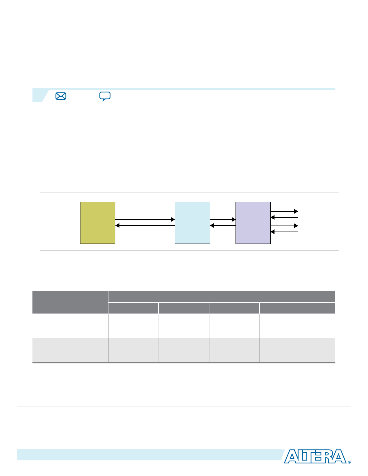
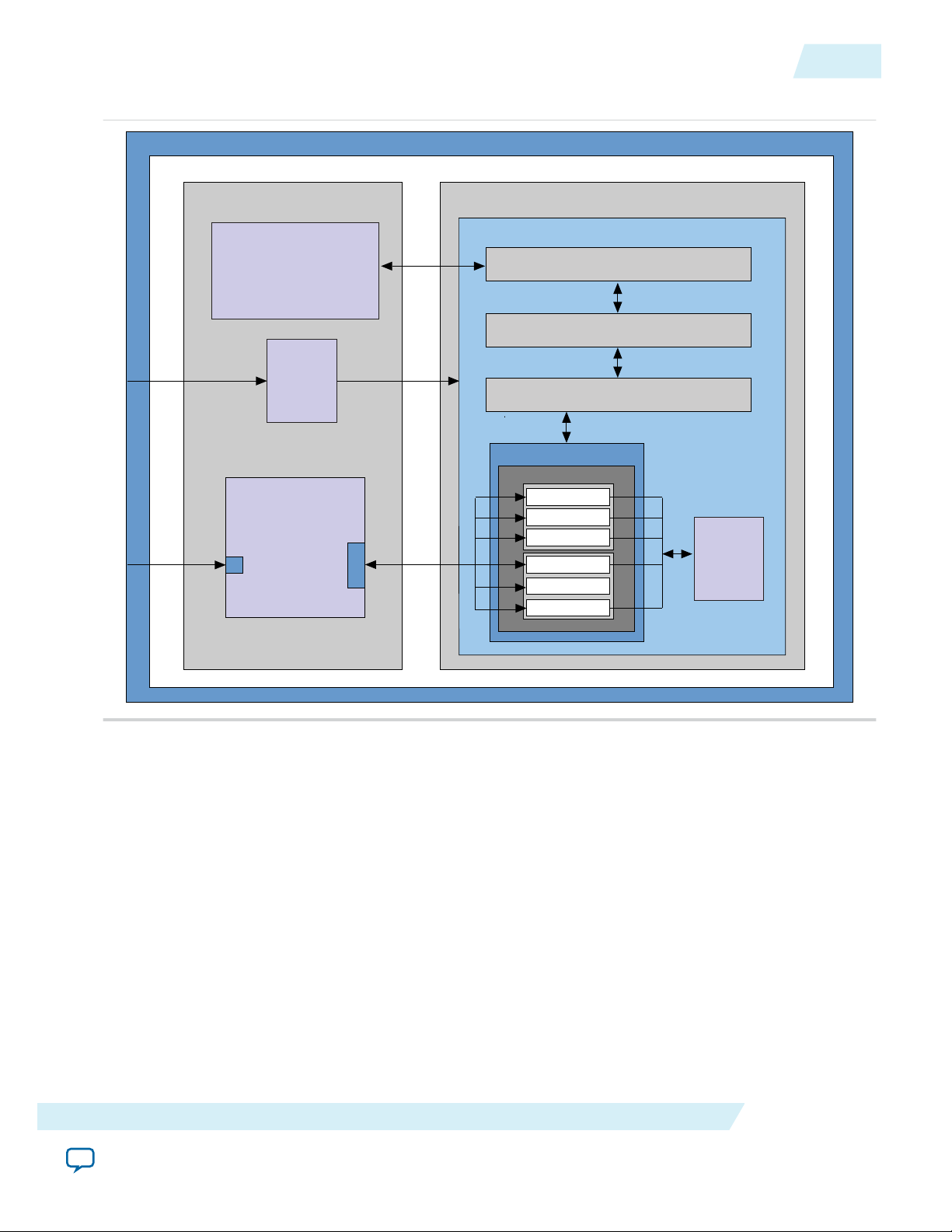
Altera® Arria® V FPGAs include a configurable, hardened protocol stack for PCI Express
compliant with PCI Express Base Specification 2.1 or 3.0. The Hard IP for PCI Express using the Avalon
Streaming (Avalon-ST) interface is the most flexible variant. However, this variant requires a thorough
understanding of the PCIe
interfaces for this variant.
Figure 1-1: Arria V PCIe Variant with Avalon-ST Interface
Table 1-1: PCI Express Data Throughput
®
Protocol. The following figure shows the high-level modules and connecting
®
that is
The following table provides bandwidths for a single transmit (TX) or receive (RX) channel. The numbers double
for duplex operation. Gen1 and Gen2 use 8B/10B encoding which introduces a 20% overhead.
PCI Express Gen1
(2.5 Gbps)
PCI Express Gen2
(5.0 Gbps)
Refer to the PCI Express High Performance Reference Design for more information about calculating
bandwidth for the hard IP implementation of PCI Express in many Altera FPGAs.
©
2014 Altera Corporation. All rights reserved. ALTERA, ARRIA, CYCLONE, ENPIRION, MAX, MEGACORE, NIOS, QUARTUS and STRATIX words and logos are
trademarks of Altera Corporation and registered in the U.S. Patent and Trademark Office and in other countries. All other words and logos identified as
trademarks or service marks are the property of their respective holders as described at www.altera.com/common/legal.html. Altera warrants performance
of its semiconductor products to current specifications in accordance with Altera's standard warranty, but reserves the right to make changes to any
products and services at any time without notice. Altera assumes no responsibility or liability arising out of the application or use of any information,
product, or service described herein except as expressly agreed to in writing by Altera. Altera customers are advised to obtain the latest version of device
specifications before relying on any published information and before placing orders for products or services.
Link Width
×1 ×2 ×4 ×8
2 4 8 16
4 8 16
N/A
ISO
9001:2008
Registered
Page 3

1-2
Features
Related Information
• PCI Express Base Specification 2.1 or 3.0
• PCI Express High Performance Reference Design
• Creating a System with Qsys
Features
New features in the Quartus® II 14.1 software release:
• Reduced Quartus II compilation warnings by 50%.
The Arria V Hard IP for PCI Express supports the following features:
• Complete protocol stack including the Transaction, Data Link, and Physical Layers implemented as
• Support for ×1, ×2, ×4, and ×8 configurations with Gen1 and Gen2 lane rates for Root Ports and
• Dedicated 16 KByte receive buffer.
• Optional hard reset controller for Gen2.
• Optional support for Configuration via Protocol (CvP) using the PCIe link allowing the I/O and core
• Qsys example designs demonstrating parameterization, design modules, and connectivity.
• Extended credit allocation settings to better optimize the RX buffer space based on application type.
• Multi-function support for up to eight Endpoint functions.
• Optional end-to-end cyclic redundancy code (ECRC) generation and checking and advanced error
2014.12.15
hard IP.
Endpoints.
bitstreams to be stored separately.
reporting (AER) for high reliability applications.
Easy to use:
• Flexible configuration.
• Substantial on-chip resource savings and guaranteed timing closure.
• No license requirement.
• Example designs to get started.
Table 1-2: Feature Comparison for all Hard IP for PCI Express IP Cores
The table compares the features of the four Hard IP for PCI Express IP Cores.
Feature Avalon‑ST Interface Avalon‑MM Interface Avalon‑MM DMA
IP Core License Free Free Free
Native Endpoint Supported Supported Supported
Legacy Endpoint
(1)
Supported Not Supported Not Supported
Root port Supported Supported Not Supported
(1)
Not recommended for new designs.
Altera Corporation
Datasheet
Send Feedback
Page 4

2014.12.15
Feature Avalon‑ST Interface Avalon‑MM Interface Avalon‑MM DMA
Gen1 ×1, ×2, ×4, ×8 ×1, ×2, ×4, ×8 x8
Gen2 ×1, ×2, ×4 ×1, ×2, ×4 ×4
Features
1-3
64-bit Application
Layer interface
128-bit Application
Layer interface
Transaction Layer
Packet type (TLP)
Supported Supported Not supported
Supported Supported Supported
• Memory Read Request
• Memory Read RequestLocked
• Memory Write Request
• I/O Read Request
• I/O Write Request
• Configuration Read
Request (Root Port)
• Configuration Write
Request (Root Port)
• Message Request
• Message Request with
Data Payload
• Completion Message
• Completion with Data
• Completion for Locked
• Memory Read Request
• Memory Write Request
• I/O Read Request—
Root Port only
• I/O Write Request—
Root Port only
• Configuration Read
Request (Root Port)
• Configuration Write
Request (Root Port)
• Completion Message
• Completion with Data
• Memory Read Request
(single dword)
• Memory Write Request
(single dword)
• Memory Read
Request
• Memory Write
Request
• Completion
Message
• Completion with
Data
Read without Data
Datasheet
Payload size 128–512 bytes 128 or 256 bytes 128 or 256 bytes
Number of tags
32 or 64 16 16
supported for nonposted requests
62.5 MHz clock Supported Supported Not Supported
Multi-function
Out-of-order
Supports up to 8 functions Supports single function
only
Supports single
function only
Not supported Supported Supported
completions
(transparent to the
Application Layer)
Send Feedback
Altera Corporation
Page 5

1-4
Release Information
Feature Avalon‑ST Interface Avalon‑MM Interface Avalon‑MM DMA
2014.12.15
Requests that cross 4
Not supported Supported Supported
KByte address
boundary (transparent
to the Application
Layer)
Polarity Inversion of
Supported Supported Supported
PIPE interface signals
ECRC forwarding on
Supported Not supported Not supported
RX and TX
Number of MSI
1, 2, 4, 8, or 16 1, 2, 4, 8, or 16 1, 2, 4, 8, or 16
requests
MSI-X Supported Supported Supported
Legacy interrupts Supported Supported Supported
Expansion ROM Supported Not supported Not supported
The purpose of the Arria V Avalon-ST Interface for PCI e Solutions User Guide is to explain how to use
this and not to explain the PCI Express protocol. Although there is inevitable overlap between these two
purposes, this document should be used in conjunction with an understanding of the PCI Express Base
Specification.
Note:
This release provides separate user guides for the different variants. The Related Information
provides links to all versions.
Related Information
• V-Series Avalon-MM DMA Interface for PCIe Solutions User Guide
• Arria V Avalon-MM Interface for PCIe Solutions User Guide
• Arria V Avalon-ST Interface for PCIe Solutions User Guide
Release Information
Table 1-3: Hard IP for PCI Express Release Information
Item Description
Version 14.1
Release Date December 2014
Altera Corporation
Datasheet
Send Feedback
Page 6

2014.12.15
Ordering Codes No ordering code is required
Product IDs There are no encrypted files for the Arria V Hard IP
Vendor ID
Device Family Support
Table 1-4: Device Family Support
Device Family Support
Arria V Final. The IP core is verified with final timing
Device Family Support
Item Description
for PCI Express. The Product ID and Vendor ID are
not required because this IP core does not require a
license.
models. The IP core meets all functional and timing
requirements for the device family and can be used
in production designs.
1-5
Other device families Refer to the Related Information below for other
device families:
Related Information
• Arria V GZ Avalon-MM Interface for PCIe Solutions User Guide
• Arria V GZ Avalon-ST Interface for PCIe Solutions User Guide
• Arria 10 Avalon-MM Interface for PCIe Solutions User Guide
• Arria 10 Avalon-MM DMA Interface for PCIe Solutions User Guide
• Arria 10 Avalon-ST Interface for PCIe Solutions User Guide
• Cyclone V Avalon-MM Interface for PCIe Solutions User Guide
• Cyclone V Avalon-ST Interface for PCIe Solutions User Guide
• IP Compiler for PCI Express User Guide
• Stratix V Avalon-MM Interface for PCIe Solutions User Guide
• Stratix V Avalon-ST Interface for PCIe Solutions User Guide
• Stratix V Avalon-ST Interface with SR-IOV for PCIe Solutions User Guide
Datasheet
Altera Corporation
Send Feedback
Page 7
Altera FPGA
User Application
Logic
PCIe
Hard IP
RP
PCIe
Hard IP
EP
User Application
Logic
PCI Express Link
Altera FPGA
1-6
Configurations
Configurations
The Arria V Hard IP for PCI Express includes a full hard IP implementation of the PCI Express stack
comprising the following layers:
• Physical (PHY), including:
• Physical Media Attachment (PMA)
• Physical Coding Sublayer (PCS)
• Media Access Control (MAC)
• Data Link Layer (DL)
• Transaction Layer (TL)
The Hard IP supports all memory, I/O, configuration, and message transactions. It is optimized for Altera
devices. The Application Layer interface is also optimized to achieve maximum effective throughput. You
can customize the Hard IP to meet your design requirements.
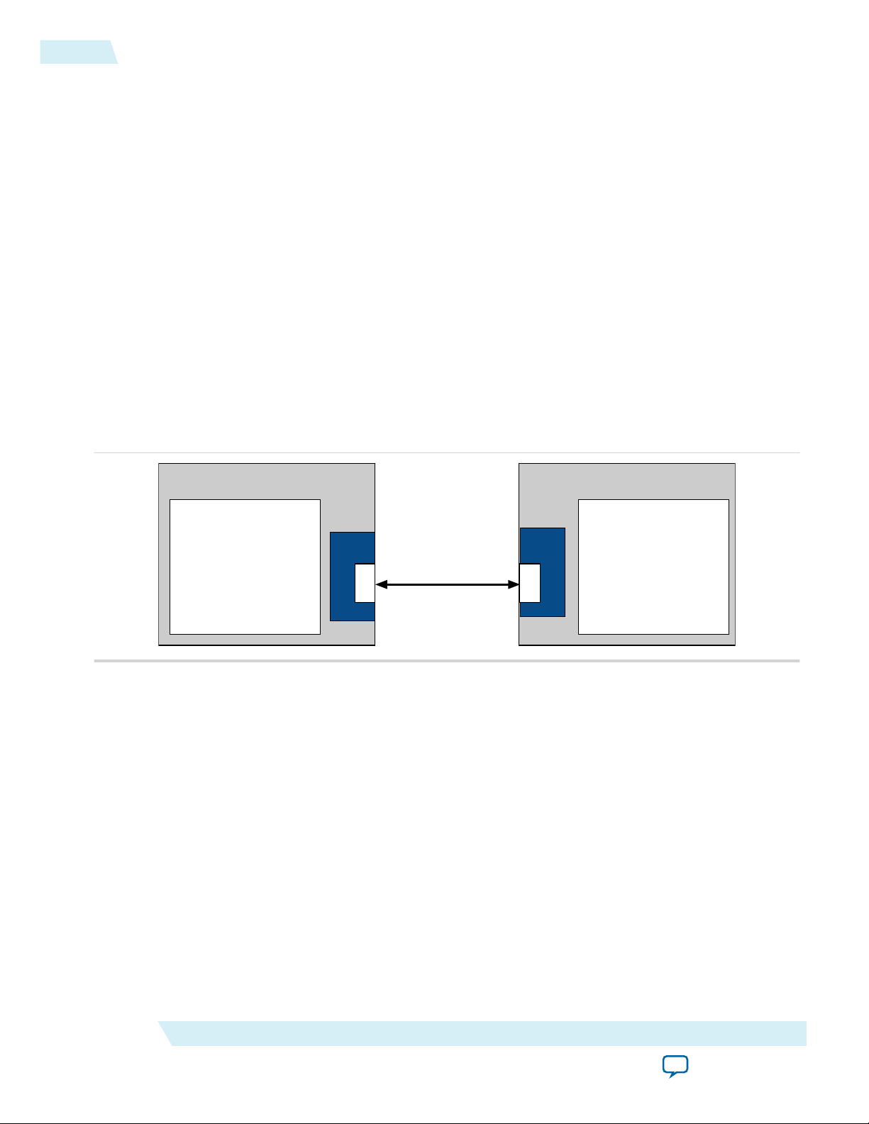
Figure 1-2: PCI Express Application with a Single Root Port and Endpoint
The following figure shows a PCI Express link between two Arria V FPGAs. One is configured as a Root
Port and the other as an Endpoint.
2014.12.15
Altera Corporation
Datasheet
Send Feedback
Page 8
Arria V or Cyclone V FPGA
PCIe Hard
IP Multi-
Function
EP
CAN GbE ATA PCI
Altera FPGA
PCIe
Hard IP
RP
Host
CPU
Memory
Controller
Peripheral
Controller
Peripheral
Controller
USB
SPI GPIO
I2C
PCI Express Link
2014.12.15
Configurations
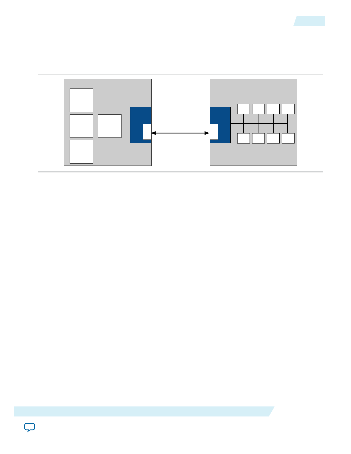
Figure 1-3: PCI Express Application with an Endpoint Using the Multi-Function Capability
The following figure shows a PCI Express link between two Altera FPGAs. One is configured as a Root
Port and the other as a multi-function Endpoint. The FPGA serves as a custom I/O hub for the host CPU.
In the Arria V FPGA, each peripheral is treated as a function with its own set of Configuration Space
registers. Eight multiplexed functions operate using a single PCI Express link.
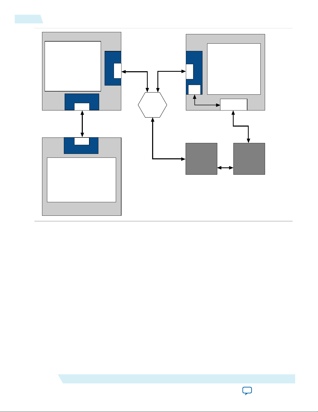
Figure 1-4: PCI Express Application Using Configuration via Protocol
1-7
The Arria V design below includes the following components:
• A Root Port that connects directly to a second FPGA that includes an Endpoint.
• Two Endpoints that connect to a PCIe switch.
• A host CPU that implements CvP using the PCI Express link connects through the switch. For more
information about configuration over a PCI Express link below.
Datasheet
Send Feedback
Altera Corporation
Page 9
PCIe Link
PCIe Hard IP
RP
Switch
PCIe
Hard IP
RP
User Application
Logic
PCIe Hard IP
EP
PCIe Link
PCIe Link
User Application
Logic
Altera FPGA with Hard IP for PCI Express
Altera FPGA with Hard IP for PCI Express
Active Serial or
Active Quad
Device Configuration
Configuration via Protocol (CvP)
using the PCI Express Link
Serial or
Quad Flash
USB
Download
cable
PCIe
Hard IP
EP
User
Application
Logic
Altera FPGA with Hard IP for PCI Express
Config
Control
CvP
USB
Host CPU
PCIe
1-8
Example Designs
2014.12.15
Related Information
• Configuration via Protocol (CvP) on page 13-1
• Configuration via Protocol (CvP)Implementation in Altera FPGAs User Guide
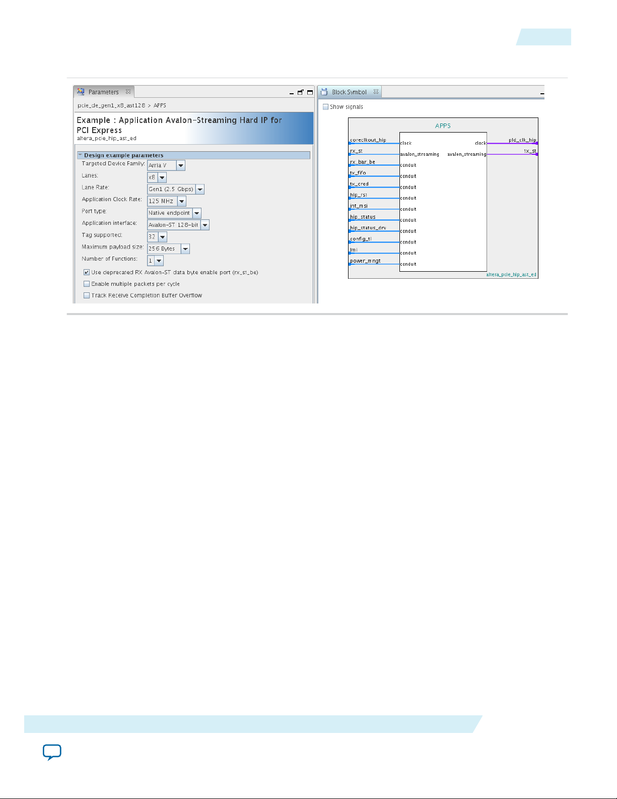
Example Designs
Altera provides example designs to familiarize you with the available functionality. Each design connects
the device under test (DUT) to an application (APPS) as the figure below illustrates. Certain critical
parameters of the APPs component are set to match the values of DUT. If you change these parameters,
you must change the APPs component to match. You can change the values for all other parameters of
the DUT without editing the APPs component.
Altera Corporation
Datasheet
Send Feedback
Page 10
2014.12.15
Figure 1-5: Example Design Preset Parameters
Debug Features
1-9
• Targeted Device Family
• Lanes
• Lane Rate
• Application Clock Rate
• Port type
• Application Interface
• Tags supported
• Maximum payload size
• Number of functions
The following example designs are available for the Arria V Hard IP for PCI Express. You can download
them from the <install_dir>/ ip/altera/altera_pcie/altera_pcie_hip_ast_ec/example_design/<dev> directory:
• pcie_de_gen1_x2_ast64.qsys
• pcie_de_gen1_x4_ast64.qsys
• pcie_de_gen1_x8_ast128.qsys
• pcie_de_rp_gen1_x4_ast64.qsys
• pcie_de_rp_gen1_x8_ast128.qsys
Click on the link below to get started with the example design provided in this user guide.
Related Information
Getting Started with the Arria V Hard IP for PCI Express on page 2-1
Debug Features
Debug features allow observation and control of the Hard IP for faster debugging of system-level
problems.
Datasheet
Send Feedback
Altera Corporation
Page 11

1-10
IP Core Verification
Related Information
Debugging on page 17-1
IP Core Verification
To ensure compliance with the PCI Express specification, Altera performs extensive verification. The
simulation environment uses multiple testbenches that consist of industry-standard bus functional
models (BFMs) driving the PCI Express link interface. Altera performs the following tests in the
simulation environment:
• Directed and pseudorandom stimuli are applied to test the Application Layer interface, Configuration
Space, and all types and sizes of TLPs
• Error injection tests that inject errors in the link, TLPs, and Data Link Layer Packets (DLLPs), and
check for the proper responses
• PCI-SIG® Compliance Checklist tests that specifically test the items in the checklist
• Random tests that test a wide range of traffic patterns
Altera provides the following two example designs that you can leverage to test your PCBs and complete
compliance base board testing (CBB testing) at PCI-SIG.
2014.12.15
Related Information
• PCI SIG Gen3 x8 Merged Design - Stratix V
• PCI SIG Gen2 x8 Merged Design - Stratix V
Compatibility Testing Environment
Altera has performed significant hardware testing to ensure a reliable solution. In addition, Altera
internally tests every release with motherboards and PCI Express switches from a variety of manufac‐
turers. All PCI-SIG compliance tests are run with each IP core release.
Performance and Resource Utilization
Because the PCIe protocol stack is implemented in hardened logic, it uses less than 1% of device
resources.
Note:
Related Information
Fitter Resources Reports
Soft calibration of the transceiver module requires additional logic. The amount of logic required
depends on the configuration.
Recommended Speed Grades
Altera Corporation
Datasheet
Send Feedback
Page 12

2014.12.15
Steps in Creating a Design for PCI Express
Table 1-5: Arria V Recommended Speed Grades for Link Widths and Application Layer Clock Frequencies
Altera recommends setting the Quartus II Analysis & Synthesis Settings Optimization Technique to Speed when
the Application Layer clock frequency is 250 MHz. For information about optimizing synthesis, refer to Setting Up
and Running Analysis and Synthesis in Quartus II Help. For more information about how to effect the
Optimization Technique settings, refer to Area and Timing Optimization in volume 2 of the Quartus II
Handbook. .
1-11
Link Rate Link Width Interface
Width
Application Clock
Frequency (MHz)
×1 64 bits 62.5
×2 64 bits 125 –4,–5,–6
Gen1
×4 64 bits 125 –4,–5,–6
×8 128 bits 125 –4,–5,–6
×1 64 bits
Gen2
×2 64 bits 125 –4,–5
×4 128 bits 125 –4,–5
Related Information
• Area and Timing Optimization
• Altera Software Installation and Licensing Manual
• Setting up and Running Analysis and Synthesis
Recommended Speed Grades
(2)
,125 –4,–5,–6
125
–4,–5
Steps in Creating a Design for PCI Express
Before you begin
Select the PCIe variant that best meets your design requirements.
• Is your design an Endpoint or Root Port?
• What Generation do you intend to implement?
• What link width do you intend to implement?
• What bandwidth does your application require?
• Does your design require CvP?
1. Select parameters for that variant.
2. Simulate using an Altera-provided example design. All of Altera's PCI Express example designs are
available under <install_dir>/ip/altera/altera_pcie/. Alternatively, create a simulation model and use your
own custom or third-party BFM. The Qsys Generate menu generates simulation models. Altera
(2)
This is a power-saving mode of operation
Datasheet
Send Feedback
Altera Corporation
Page 13

1-12
Steps in Creating a Design for PCI Express
2014.12.15
supports ModelSim®-Altera for all IP. The PCIe cores support the Aldec RivieraPro, Cadence NCsim,
Mentor Graphics ModelSim, and Synopsys VCS and VCS-MX simulators.
3. Compile your design using the Quartus II software. If the versions of your design and the Quartus II
software you are running do not match, regenerate your PCIe design.
4. Download your design to an Altera development board or your own PCB. Click on the All Develop‐
ment Kits link below for a list of Altera's development boards.
5. Test the hardware. You can use Altera's SignalTap® II Logic Analyzer or a third-party protocol
analyzer to observe behavior.
6. Substitute your Application Layer logic for the Application Layer logic in Altera's testbench. Then
repeat Steps 3–6. In Altera's testbenches, the PCIe core is typically called the DUT (device under test).
The Application Layer logic is typically called APPS.
Related Information
• Parameter Settings on page 3-1
• Getting Started with the Arria V Hard IP for PCI Express on page 2-1
• All Development Kits
Altera Corporation
Datasheet
Send Feedback
Page 14
Getting Started with the Arria V Hard IP for PCI
APPS
altpcied_<dev>_hwtcl.v
Hard IP for PCI Express Testbench for Endpoints
Avalon-ST TX
Avalon-ST RX
reset
status
Avalon-ST TX
Avalon-ST RX
reset
status
DUT
altpcie_<dev>_hip_ast_hwtcl.v
Root Port Model
altpcie_tbed_<dev>_hwtcl.v
PIPE or
Serial
Interface
Root Port BFM
altpcietb_bfm_rpvar_64b_x8_pipen1b
Root Port Driver and Monitor
altpcietb_bfm_vc_intf
www.altera.com
101 Innovation Drive, San Jose, CA 95134
Express
2014.12.15
Subscribe
This section provides instructions to help you quickly customize, simulate, and compile the Arria V Hard
IP for PCI Express IP Core. When you install the Quartus II software you also install the IP Library. This
installation includes design examples for Hard IP for PCI Express under the <install_dir>/ip/altera/altera_
pcie/ directory.
After you install the Quartus II software for 14.0, you can copy the design examples from the <install_dir>/
ip/altera/altera_pcie/altera_pcie/altera_pcie_hip_ast_ed/example_designs/<dev> directory. This walkthrough
uses the Gen1 ×4 Endpoint, pcie_de_gen1_x4_ast64.qsys. The following figure illustrates the top-level
modules of the testbench in which the DUT, a Gen1 Endpoint, connects to a chaining DMA engine,
labeled APPS in the following figure, and a Root Port model. The simulation can use the parallel PHY
Interface for PCI Express (PIPE) or serial interface.
Figure 2-1: Testbench for an Endpoint
Send Feedback
2
Altera provides example designs to help you get started with the Arria V Hard IP for PCI Express IP Core.
You can use example designs as a starting point for your own design. The example designs include scripts
to compile and simulate the Arria V Hard IP for PCI Express IP Core. This example design provides a
simple method to perform basic testing of the Application Layer logic that interfaces to the Hard IP for
PCI Express.
©
2014 Altera Corporation. All rights reserved. ALTERA, ARRIA, CYCLONE, ENPIRION, MAX, MEGACORE, NIOS, QUARTUS and STRATIX words and logos are
trademarks of Altera Corporation and registered in the U.S. Patent and Trademark Office and in other countries. All other words and logos identified as
trademarks or service marks are the property of their respective holders as described at www.altera.com/common/legal.html. Altera warrants performance
of its semiconductor products to current specifications in accordance with Altera's standard warranty, but reserves the right to make changes to any
products and services at any time without notice. Altera assumes no responsibility or liability arising out of the application or use of any information,
product, or service described herein except as expressly agreed to in writing by Altera. Altera customers are advised to obtain the latest version of device
specifications before relying on any published information and before placing orders for products or services.
ISO
9001:2008
Registered
Page 15

2-2
Qsys Design Flow
For a detailed explanation of this example design, refer to the Testbench and Design Example chapter. If
you choose the parameters specified in this chapter, you can run all of the tests included in Testbench and
Design Example chapter.
For more information about Qsys, refer to System Design with Qsys in the Quartus II Handbook. For more
information about the Qsys GUI, refer to About Qsys in Quartus II Help.
Related Information
• System Design with Qsys
• About Qsys
Qsys Design Flow
Copy the pcie_de_gen1_x4_ast64.qsys design example from the <install_dir>/ip/altera/altera_pcie/altera_
pcie/altera_pcie_hip_ast_ed/example_designs/<dev> to your working directory. The following figure
illustrates this Qsys system.
2014.12.15
Altera Corporation
Getting Started with the Arria V Hard IP for PCI Express
Send Feedback
Page 16
2014.12.15
Qsys Design Flow
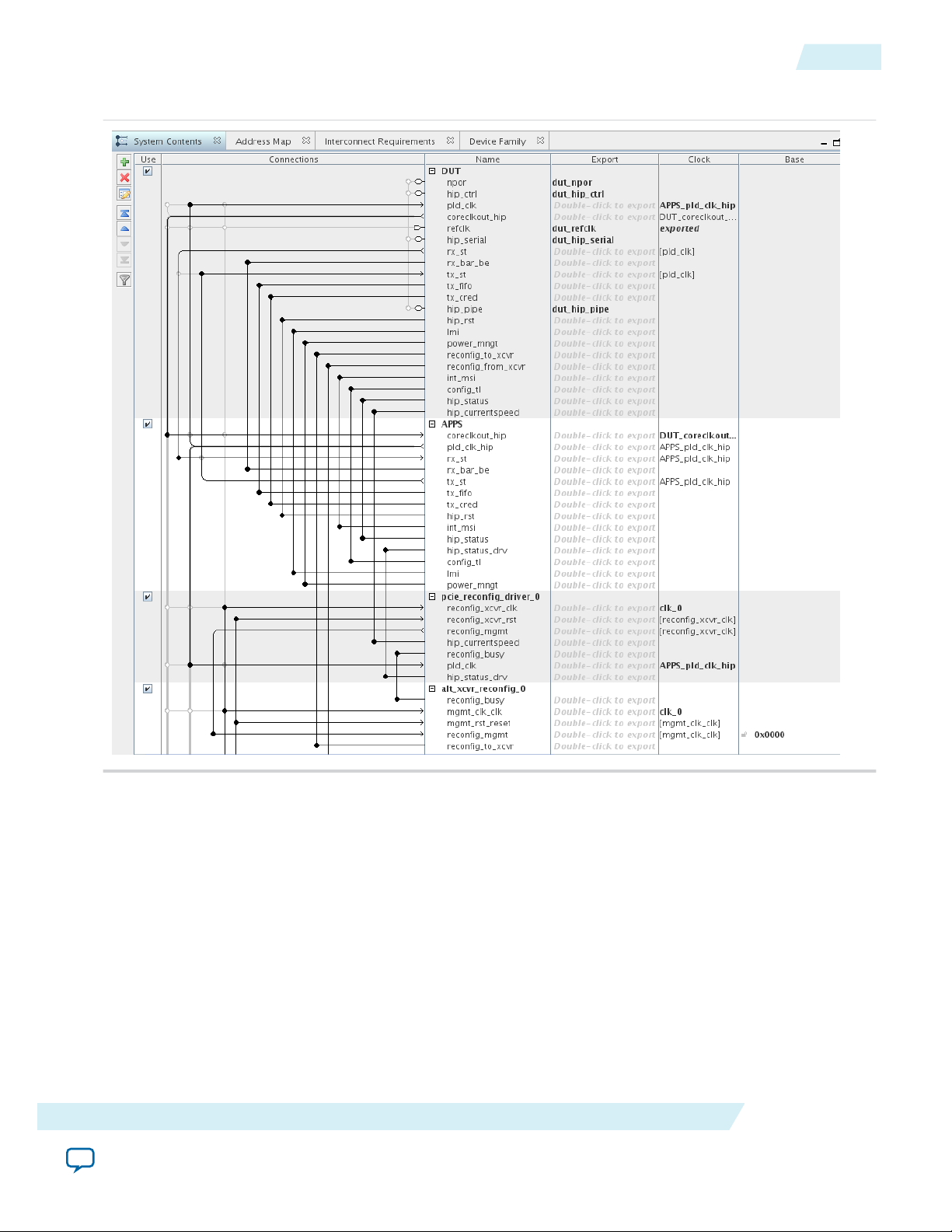
Figure 2-2: Complete Gen1 ×4 Endpoint (DUT) Connected to Example Design (APPS)
2-3
The example design includes the following components:
• DUT—This is Gen1 ×4 Endpoint. For your own design, you can select the data rate, number of lanes,
and either Endpoint or Root Port mode.
• APPS—This DMA driver configures the DUT and drives read and write TLPs to test DUT function‐
ality.
• pcie_reconfig_driver_0—This Avalon-MM master drives the Transceiver Reconfiguration Controller.
The pcie_reconfig_driver_0 is implemented in clear text that you can modify if your design requires
different reconfiguration functions. After you generate your Qsys system, the Verilog HDL for this
component is available as: <working_dir>/<variant_name>/testbench/<variant_name>_tb/simulation/
submodules/altpcie_reconfig_driver.sv.
• Transceiver Reconfiguration Controller—The Transceiver Reconfiguration Controller dynamically
reconfigures analog settings to improve signal quality. For Gen1 and Gen2 data rates, the Transceiver
Reconfiguration Controller must perform offset cancellation and PLL calibration.
Getting Started with the Arria V Hard IP for PCI Express
Send Feedback
Altera Corporation
Page 17

2-4
Generating the Testbench
Generating the Testbench
Follow these steps to generate the chaining DMA testbench:
1. On the Generate menu, select Generate Testbench System. Specify the parameters listed in the
following table.
Table 2-1: Parameters to Specify on the Generation Tab in Qsys
Parameter Value
Create testbench Qsys system Standard, BFMs for standard Qsys interfaces
Create testbench simulation model Verilog
Allow mixed-language simulation Turn this option off
Output Directory
Path <working_dir>/pcie_de_gen1_x4_ast64
2014.12.15
Testbench <working_dir>/pcie_de_gen1_x4_ast64/testbench
2. Click the Generate button at the bottom of the Generation tab to create the testbench.
Simulating the Example Design
1. Start your simulation tool. This example uses the ModelSim® software.
2. From the ModelSim transcript window, in the testbench directory type the following commands:
a. do msim_setup.tcl
b. ld_debug (This command compiles all design files and elaborates the top-level design without any
optimization.)
c. run -all
The simulation includes the following stages:
• Link training
• Configuration
• DMA reads and writes
• Root Port to Endpoint memory reads and writes
Disabling Scrambling to Interpret TLPs at the PIPE Interface
1. Go to <project_directory/<variant>/testbench/<variant>_tb/simulation/submodules/.
2. Open altpcietb_bfm_top_rp.v.
3. Locate the declaration of test_in[2:1]. Set test_in[2] = 1 and test_in[1] = 0. Changing
test_in[2] = 1 disables data scrambling on the PIPE interface.
4. Save altpcietb_bfm_top_rp.v.
Altera Corporation
Getting Started with the Arria V Hard IP for PCI Express
Send Feedback
Page 18

2014.12.15
Generating Quartus II Synthesis Files
1. On the Generate menu, select Generate HDL.
2. For Create HDL design files for synthesis, select Verilog.
You can leave the default settings for all other items.
3. Click Generate to generate files for Quartus II synthesis.
4. Click Finish when the generation completes.
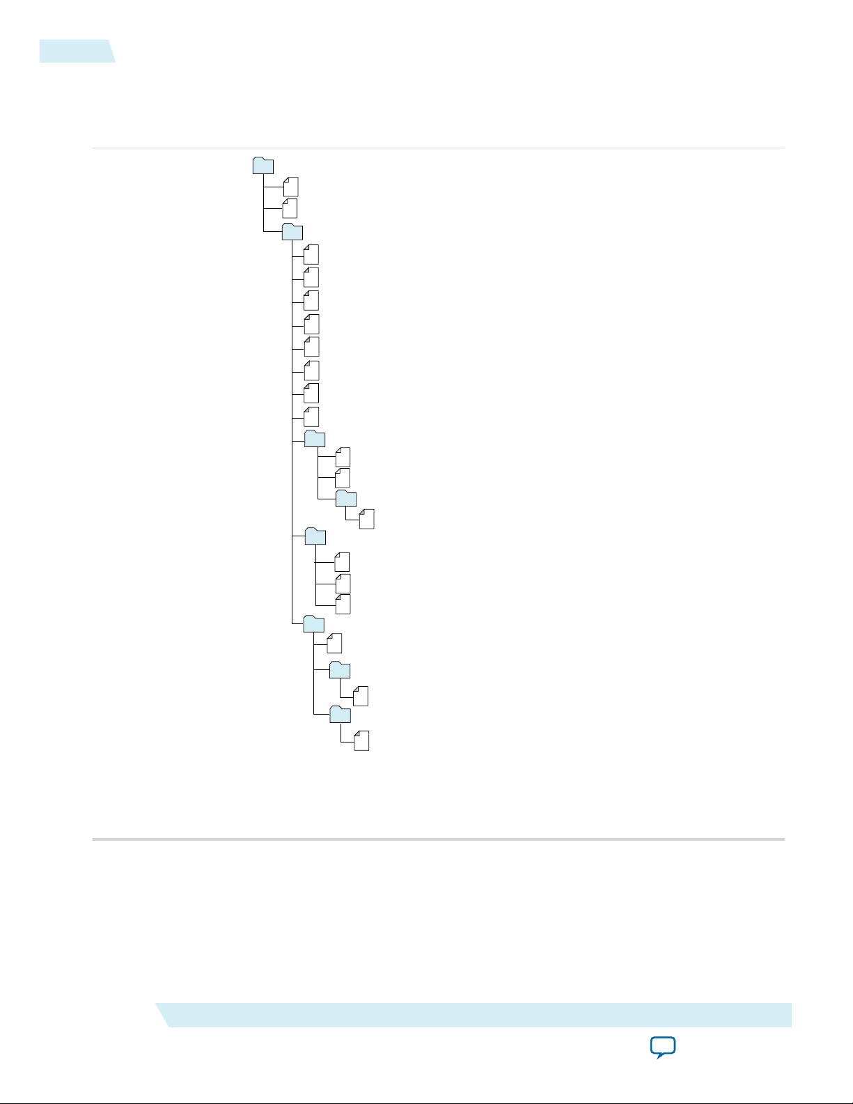
Understanding the Files Generated
Table 2-2: Overview of Qsys Generation Output Files
Directory Description
<testbench_dir>/<variant_name>/synthesis Includes the top-level HDL file for the Hard IP for
Generating Quartus II Synthesis Files
PCI Express and the .qip file that lists all of the
necessary assignments and information required to
process the IP core in the Quartus II compiler.
Generally, a single .qip file is generated for each IP
core.
2-5
<testbench_dir>/<variant_name>/synthesis/submodules
Includes the HDL files necessary for Quartus II
synthesis.
<testbench_dir>/<variant_name>/testbench
Includes testbench subdirectories for the Aldec,
Cadence, Synopsys, and Mentor simulation tools
with the required libraries and simulation scripts.
<testbench_dir>/<variant_name>/testbench<cad_
vendor>
Includes the HDL source files and scripts for the
simulation testbench.
For a more detailed listing of the directories and files the Quartus II software generates, refer to Files
Generated for Altera IP Cores in Compiling the Design in the Qsys Design Flow.
Understanding Physical Placement of the PCIe IP Core
For more information about physical placement of the PCIe blocks, refer to the links below. Contact your
Altera sales representative for detailed information about channel and PLL usage.
Related Information
• Physical Layout of Hard IP in Arria V Devices on page 4-49
• Channel Placement in Arria V Devices on page 4-52
Compiling the Design in the Quartus II Software
To compile the Qsys design example in the Quartus II software, you must create a Quartus II project and
add your Qsys files to that project.
Getting Started with the Arria V Hard IP for PCI Express
Send Feedback
Altera Corporation
Page 19

2-6
Compiling the Design in the Quartus II Software
Complete the following steps to create your Quartus II project:
1. Click the New Project Wizard icon.
2. Click Next in the New Project Wizard: Introduction (The introduction does not appear if you
previously turned it off)
3. On the Directory, Name, Top-Level Entity page, enter the following information:
a. The working directory shown is correct. You do not have to change it.
b. For the project name, browse to the synthesis directory that includes your Qsys project,
<working_dir>/pcie_de_gen1_x4_ast64/synthesis. Select your variant name, pcie_de_gen1_x4_ast64.v .
Then, click Open.
c. If the top-level design entity and Qsys system names are identical, the Quartus II software treats the
Qsys system as the top-level design entity.
4. Click Next to display the Add Files page.
5. Complete the following steps to add the Quartus II IP File (.qip)to the project:
a. Click the browse button. The Select File dialog box appears.
b. In the Files of type list, select IP Variation Files (*.qip).
c. Browse to the <working_dir>/pcie_de_gen1_x4_ast64/synthesis directory.
d. Click pcie_de_gen1_x4_ast64.qip and then click Open.
e. On the Add Files page, click Add, then click OK.
6. Click Next to display the Device page.
7. On the Family & Device Settings page, choose the following target device family and options:
2014.12.15
a. In the Family list, select Arria V (GT/GX/ST/SX).
b. In the Devices list, select Arria V GX Extended Features..
c. In the Available Devices list, select 5AGXFB3H6F35C6.
8. Click Next to close this page and display the EDA Tool Settings page.
9. From the Simulation list, select ModelSim®. From the Format list, select the HDL language you
intend to use for simulation.
10.Click Next to display the Summary page.
11.Check the Summary page to ensure that you have entered all the information correctly.
12.Click Finish to create the Quartus II project.
13.Add the Synopsys Design Constraint (SDC) commands shown in the following example to the
top-level design file for your Quartus II project.
14.To compile your design using the Quartus II software, on the Processing menu, click Start Compila‐
tion. The Quartus II software then performs all the steps necessary to compile your design.
15.After compilation, expand the TimeQuest Timing Analyzer folder in the Compilation Report. Note
whether the timing constraints are achieved in the Compilation Report.
16.If your design does not initially meet the timing constraints, you can find the optimal Fitter settings for
your design by using the Design Space Explorer. To use the Design Space Explorer, click Launch
Design Space Explorer on the tools menu.
Example 2-1: Synopsys Design Constraints
Altera Corporation
create_clock -period “100 MHz” -name {refclk_pci_express}{*refclk_*}
derive_pll_clocks
derive_clock_uncertainty
Getting Started with the Arria V Hard IP for PCI Express
Send Feedback
Page 20

2014.12.15
Compiling the Design in the Quartus II Software
# PHY IP reconfig controller constraints
# Set reconfig_xcvr clock
# Modify to match the actual clock pin name
# used for this clock, and also changed to have the correct period set
create_clock -period "125 MHz" -name {reconfig_xcvr_clk}{*reconfig_xcvr_clk*}
# HIP Soft reset controller SDC constraints
set_false_path -to [get_registers* altpcie_rs_serdes|fifo_err_sync_r[0]]
set_false_path -from [get_registers *sv_xcvr_pipe_native*] -to[get_registers
*altpcie_rs_serdes|*]
# Hard IP testin pins SDC constraints
set_false_path -from [get_pins -compatibilitly_mode *hip_ctrl*]
2-7
Getting Started with the Arria V Hard IP for PCI Express
Send Feedback
Altera Corporation
Page 21
Notes:
1. If supported and enabled for your IP variation
2. If functional simulation models are generated
<Project Directory>
<your_ip>_bb.v - Verilog HDL black box EDA synthesis file
<your_ip>_inst.v or .vhd - Sample instantiation template
synthesis - IP synthesis files
<your_ip>.qip - Lists files for synthesis
testbench - Simulation testbench files
1
<testbench_hdl_files>
<simulator_vendor> - Testbench for supported simulators
<simulation_testbench_files>
<your_ip>.v or .vhd - Top-level IP variation synthesis file
simulation - IP simulation files
<your_ip>.sip - NativeLink simulation integration file
<simulator vendor> - Simulator setup scripts
<simulator_setup_scripts>
<your_ip> - IP core variation files
<your_ip>.qip or .qsys - System or IP integration file
<your_ip>_generation.rpt - IP generation report
<your_ip>.bsf - Block symbol schematic file
<your_ip>.ppf - XML I/O pin information file
<your_ip>.spd - Combines individual simulation startup scripts
1
<your_ip>.html - Contains memory map
<your_ip>.sopcinfo - Software tool-chain integration file
<your_ip>_syn.v or .vhd - Timing & resource estimation netlist
1
<your_ip>.debuginfo - Lists files for synthesis
<your_ip>.v, .vhd, .vo, .vho - HDL or IPFS models
2
<your_ip>_tb - Testbench for supported simulators
<your_ip>_tb.v or .vhd - Top-level HDL testbench file
2-8
Modifying the Example Design
Files Generated for Altera IP Cores
Figure 2-3: IP Core Generated Files
The Quartus II software generates the following output for your IP core.
2014.12.15
Modifying the Example Design
To use this example design as the basis of your own design, replace the Chaining DMA Example shown in
the following figure with your own Application Layer design. Then modify the Root Port BFM driver to
generate the transactions needed to test your Application Layer.
Altera Corporation
Getting Started with the Arria V Hard IP for PCI Express
Send Feedback
Page 22
PCB
Avalon-MM slave
Reset
Hard IP for PCI Express
Altera FPGA
PCB
Transaction Layer
Data Link Layer
PHY MAC Layer
x4 PCIe Link
(Physical Layer)
PHY IP Core for PCI Express
Lane 2
Lane 3
Lane 4
Lane 1
Lane 0
TX PLL
Transceiver Bank
S
Reconfig
to and from
Transceiver
to and from
Embedded
Controller
(Avalon-MM
slave interface)
Transceiver
Reconfiguration
Controller
Root
Port
BFM
npor
Reset
APPS DUT
Chaining DMA
(User Application)
2014.12.15
Using the IP Catalog To Generate Your Arria V Hard IP for PCI Express as a Separate
Figure 2-4: Testbench for PCI Express
2-9
Component
Using the IP Catalog To Generate Your Arria V Hard IP for PCI Express as a Separate Component
You can also instantiate the Arria V Hard IP for PCI Express IP Core as a separate component for
integration into your project.
Getting Started with the Arria V Hard IP for PCI Express
You can use the Quartus II IP Catalog and IP Parameter Editor to select, customize, and generate files
representing your custom IP variation. The IP Catalog (Tools > IP Catalog) automatically displays IP
cores available for your target device. Double-click any IP core name to launch the parameter editor and
generate files representing your IP variation.
For more information about the customizing and generating IP Cores refer to Specifying IP Core
Parameters and Options in Introduction to Altera IP Cores. For more information about upgrading older
IP cores to the current release, refer to Upgrading Outdated IP Cores in Introduction to Altera IP Cores.
Send Feedback
Altera Corporation
Page 23

2-10
Using the IP Catalog To Generate Your Arria V Hard IP for PCI Express as a Separate
Component
2014.12.15
Note: Your design must include the Transceiver Reconfiguration Controller IP Core and the Altera PCIe
Reconfig Driver. Refer to the figure in the Qsys Design Flow section to learn how to connect this
components.
Related Information
• Introduction to Altera IP Cores
• Managing Quartus II Projects
Altera Corporation
Getting Started with the Arria V Hard IP for PCI Express
Send Feedback
Page 24

2014.12.15
www.altera.com
101 Innovation Drive, San Jose, CA 95134
Parameter Settings
3
Subscribe
Send Feedback
Avalon-ST System Settings
Table 3-1: System Settings for PCI Express
Parameter Value Description
Number of Lanes ×1, ×2, ×4, ×8 Specifies the maximum number of lanes supported.
Lane Rate Gen1 (2.5 Gbps)
Gen2 (2.5/5.0 Gbps)
Port type Root Port
Native Endpoint
Legacy Endpoint
Specifies the maximum data rate at which the link can operate.
Specifies the port type. Altera recommends Native Endpoint
for all new Endpoint designs. Select Legacy Endpoint only
when you require I/O transaction support for compatibility.
The Legacy Endpoint is not available for the Avalon-MM
Arria V Hard IP for PCI Express.
The Endpoint stores parameters in the Type 0 Configuration
Space. The Root Port stores parameters in the Type 1 Configu‐
ration Space.
©
2014 Altera Corporation. All rights reserved. ALTERA, ARRIA, CYCLONE, ENPIRION, MAX, MEGACORE, NIOS, QUARTUS and STRATIX words and logos are
trademarks of Altera Corporation and registered in the U.S. Patent and Trademark Office and in other countries. All other words and logos identified as
trademarks or service marks are the property of their respective holders as described at www.altera.com/common/legal.html. Altera warrants performance
of its semiconductor products to current specifications in accordance with Altera's standard warranty, but reserves the right to make changes to any
products and services at any time without notice. Altera assumes no responsibility or liability arising out of the application or use of any information,
product, or service described herein except as expressly agreed to in writing by Altera. Altera customers are advised to obtain the latest version of device
specifications before relying on any published information and before placing orders for products or services.
ISO
9001:2008
Registered
Page 25
3-2
Avalon-ST System Settings
Parameter Value Description
2014.12.15
Application
Interface
RX Buffer credit
allocation performance for
received requests
Avalon-ST 64-bit
Avalon-ST 128-bit
Minimum
Low
Balanced
High
Maximum
Specifies the width of the Avalon-ST interface between the
Application and Transaction Layers. The following widths are
required:
Data Rate Link Width Interface Width
×1 64 bits
×2 64 bits
Gen1
×4 64 bits
×8 128 bits
×1 64 bits
Gen2
×2 64 bits
×4 128 bits
Determines the allocation of posted header credits, posted
data credits, non-posted header credits, completion header
credits, and completion data credits in the 16 KByte RX buffer.
The 5 settings allow you to adjust the credit allocation to
optimize your system. The credit allocation for the selected
setting displays in the message pane.
Refer to the Throughput Optimization chapter for more
information about optimizing performance. The Flow Control
chapter explains how the RX credit allocation and the
Maximum payload RX Buffer credit allocation and the
Maximum payload size that you choose affect the allocation
of flow control credits. You can set the Maximum payload
size parameter on the Device tab.
Altera Corporation
The Message window of the GUI dynamically updates the
number of credits for Posted, Non-Posted Headers and Data,
and Completion Headers and Data as you change this
selection.
Parameter Settings
Send Feedback
Page 26

2014.12.15
Avalon-ST System Settings
Parameter Value Description
• Minimum RX Buffer credit allocation -performance for
received requests–This setting configures the minimum
PCIe specification allowed for non-posted and posted
request credits, leaving most of the RX Buffer space for
received completion header and data. Select this option for
variations where application logic generates many read
requests and only infrequently receives single requests
from the PCIe link.
• Low–This setting configures a slightly larger amount of RX
Buffer space for non-posted and posted request credits, but
still dedicates most of the space for received completion
header and data. Select this option for variations where
application logic generates many read requests and
infrequently receives small bursts of requests from the
PCIe link. This option is recommended for typical
endpoint applications where most of the PCIe traffic is
generated by a DMA engine that is located in the endpoint
application layer logic.
• Balanced–This setting allocates approximately half the RX
Buffer space to received requests and the other half of the
RX Buffer space to received completions. Select this option
for variations where the received requests and received
completions are roughly equal.
• High–This setting configures most of the RX Buffer space
for received requests and allocates a slightly larger than
minimum amount of space for received completions. Select
this option where most of the PCIe requests are generated
by the other end of the PCIe link and the local application
layer logic only infrequently generates a small burst of read
requests. This option is recommended for typical root port
applications where most of the PCIe traffic is generated by
DMA engines located in the endpoints.
• Maximum–This setting configures the minimum PCIe
specification allowed amount of completion space, leaving
most of the RX Buffer space for received requests. Select
this option when most of the PCIe requests are generated
by the other end of the PCIe link and the local application
layer logic never or only infrequently generates single read
requests. This option is recommended for control and
status endpoint applications that don't generate any PCIe
requests of their own and only are the target of write and
read requests from the root complex.
3-3
Parameter Settings
Send Feedback
Altera Corporation
Page 27

3-4
Link Capabilities
Parameter Value Description
2014.12.15
Reference clock
frequency
Use 62.5 MHz
application clock
Use deprecated
RX Avalon-ST
data byte enable
port (rx_st_be)
Enable configu‐
ration via PCIe
link
Enable Hard IP
Reconfiguration
100 MHz
125 MHz
The PCI Express Base Specification requires a
100 MHz ±300 ppm reference clock. The 125 MHz reference
clock is provided as a convenience for systems that include a
125 MHz clock source.
On/Off This mode is only available only for Gen1 ×1.
On/Off This parameter is only available for the Avalon-ST Arria V
Hard IP for PCI Express.
On/Off When On, the Quartus II software places the Endpoint in the
location required for configuration via protocol (CvP). For
more information about CvP, click the Configuration via
Protocol (CvP) link below.
On/Off When On, you can use the Hard IP reconfiguration bus to
dynamically reconfigure Hard IP read-only registers. For more
information refer to Hard IP Reconfiguration Interface. This
parameter is not available for the Avalon-MM IP Cores.
Number of
1–8 Specifies the number of functions that share the same link.
Functions
Related Information
• Configuration via Protocol (CvP) on page 13-1
• Throughput Optimization on page 11-1
• PCI Express Base Specification 2.1 or 3.0
Link Capabilities
Table 3-2: Link Capabilities
Parameter Value Description
Link port
number
0x01 Sets the read-only value of the port number field in the Link
Capabilities Register.
Altera Corporation
Parameter Settings
Send Feedback
Page 28

2014.12.15
Port Function Parameters Shared Across All Port Functions
Parameter Value Description
3-5
Slot clock
configuration
On/Off When On, indicates that the Endpoint or Root Port uses the
same physical reference clock that the system provides on the
connector. When Off, the IP core uses an independent clock
regardless of the presence of a reference clock on the
connector.
Port Function Parameters Shared Across All Port Functions
Device Capabilities
Table 3-3: Capabilities Registers
Parameter Possible Values Default Value Description
Maximum
payload size
Number of
tags
supported
per
function
128 bytes
256 bytes
512 bytes
32
64
128 bytes Specifies the maximum payload size supported. This
parameter sets the read-only value of the max payload
size supported field of the Device Capabilities register
(0x084[2:0]). Address: 0x084.
32 - Avalon-ST Indicates the number of tags supported for non-posted
requests transmitted by the Application Layer. This
parameter sets the values in the Device Control register
(0x088) of the PCI Express capability structure
described in Table 9–9 on page 9–5.
Completion
timeout
range
Parameter Settings
ABCD
BCD
ABC
The Transaction Layer tracks all outstanding
completions for non-posted requests made by the
Application Layer. This parameter configureTags
supportedes the Transaction Layer for the maximum
number to track. The Application Layer must set the tag
values in all non-posted PCI Express headers to be less
than this value. Values greater than 32 also set the
extended tag field supported bit in the Configuration
Space Device Capabilities register. The Application
Layer can only use tag numbers greater than 31 if
configuration software sets the Extended Tag Field
Enable bit of the Device Control register. This bit is
available to the Application Layer on the tl_cfg_ctl
output signal as cfg_devcsr[8].
ABCD Indicates device function support for the optional
completion timeout programmability mechanism. This
mechanism allows system software to modify the
completion timeout value. This field is applicable only to
Altera Corporation
Send Feedback
Page 29

3-6
Device Capabilities
Parameter Possible Values Default Value Description
2014.12.15
AB
B
A
None
Root Ports and Endpoints that issue requests on their
own behalf. Completion timeouts are specified and
enabled in the Device Control 2 register (0x0A8) of the
PCI Express Capability Structure Version. For all other
functions this field is reserved and must be hardwired to
0x0000b. Four time value ranges are defined:
• Range A: 50 us to 10 ms
• Range B: 10 ms to 250 ms
• Range C: 250 ms to 4 s
• Range D: 4 s to 64 s
Bits are set to show timeout value ranges supported. The
function must implement a timeout value in the range
50 s to 50 ms. The following values specify the range:
• None – Completion timeout programming is not
supported
• 0001 Range A
• 0010 Range B
• 0011 Ranges A and B
• 0110 Ranges B and C
• 0111 Ranges A, B, and C
• 1110 Ranges B, C and D
• 1111 Ranges A, B, C, and D
Implement
completion
timeout
disable
All other values are reserved. Altera recommends that
the completion timeout mechanism expire in no less
than 10 ms.
On/Off On For Endpoints using PCI Express version 2.1 or 3.0, this
option must be On. The timeout range is selectable.
When On, the core supports the completion timeout
disable mechanism via the PCI Express Device
Control Register 2. The Application Layer logic must
implement the actual completion timeout mechanism
for the required ranges.
Altera Corporation
Parameter Settings
Send Feedback
Page 30

2014.12.15
Error Reporting
Table 3-4: Error Reporting
Parameter Value Default Value Description
Error Reporting
3-7
Advanced
error
reporting
(AER)
ECRC
checking
ECRC
generation
ECRC
forwarding
On/Off Off When On, enables the Advanced Error Reporting (AER)
capability.
On/Off Off When On, enables ECRC checking. Sets the read-only
value of the ECRC check capable bit in the Advanced
Error Capabilities and Control Register. This
parameter requires you to enable the AER capability.
On/Off Off When On, enables ECRC generation capability. Sets the
read-only value of the ECRC generation capable bit in
the Advanced Error Capabilities and Control
Register. This parameter requires you to enable the
AER capability.
Not applicable for Avalon-MM DMA.
On/Off Off When On, enables ECRC forwarding to the Application
Layer. On the Avalon-ST RX path, the incoming TLP
contains the ECRC dword
(3)
and the TD bit is set if an
ECRC exists. On the transmit the TLP from the Applica‐
tion Layer must contain the ECRC dword and have the
TD bit set.
Link Capabilities
Table 3-5: Link Capabilities
Parameter Value Description
Link port
number
(3)
Throughout this user guide, the terms word, dword and qword have the same meaning that they have in
the PCI Express Base Specification. A word is 16 bits, a dword is 32 bits, and a qword is 64 bits.
Parameter Settings
Send Feedback
Not applicable for Avalon-MM DMA.
0x01 Sets the read-only value of the port number field in the Link
Capabilities Register.
Altera Corporation
Page 31

31 19 1 8 17 16 1 5 14
7
6 5
Physical Slot Number
No Command Completed Support
Electromechanical Interlock Present
Slot Power Limit Scale
Slot Power Limit Value
Hot-Plug Capable
Hot-Plug Surprise
Power Indicator Present
Attention Indicator Present
MRL Sensor Present
Power Controller Present
Attention Button Present
04 3 2 1
3-8
Slot Capabilities
Parameter Value Description
2014.12.15
Slot clock
configuration
On/Off When On, indicates that the Endpoint or Root Port uses the
same physical reference clock that the system provides on the
connector. When Off, the IP core uses an independent clock
regardless of the presence of a reference clock on the
connector.
Slot Capabilities
Table 3-6: Slot Capabilities
Parameter Value Description
Use Slot register On/Off The slot capability is required for Root Ports if a slot is implemented
on the port. Slot status is recorded in the PCI Express Capabili-
ties register. This parameter is only supported in Root Port mode.
Defines the characteristics of the slot. You turn on this option by
selecting Enable slot capability. The various bits are defined as
follows:
Slot power scale
Slot power limit
Altera Corporation
0–3
0–255
Specifies the scale used for the Slot power limit. The following
coefficients are defined:
• 0 = 1.0x
• 1 = 0.1x
• 2 = 0.01x
• 3 = 0.001x
The default value prior to hardware and firmware initialization is
b’00. Writes to this register also cause the port to send the Set_
Slot_Power_Limit Message.
Refer to Section 6.9 of the PCI Express Base Specification Revision for
more information.
In combination with the Slot power scale value, specifies the upper
limit in watts on power supplied by the slot. Refer to Section 7.8.9 of
the PCI Express Base Specification for more information.
Parameter Settings
Send Feedback
Page 32

2014.12.15
Parameter Value Description
Power Management
3-9
Slot number
Related Information
0-8191
Specifies the slot number.
PCI Express Base Specification Revision 2.1 or 3.0
Power Management
Table 3-7: Power Management Parameters
Parameter Value Description
Endpoint L0s
acceptable
latency
Maximum of 64 ns
Maximum of 128 ns
Maximum of 256 ns
Maximum of 512 ns
Maximum of 1 us
Maximum of 2 us
Maximum of 4 us
No limit
This design parameter specifies the maximum acceptable
latency that the device can tolerate to exit the L0s state for any
links between the device and the root complex. It sets the
read-only value of the Endpoint L0s acceptable latency field of
the Device Capabilities Register (0x084).
This Endpoint does not support the L0s or L1 states. However,
in a switched system there may be links connected to switches
that have L0s and L1 enabled. This parameter is set to allow
system configuration software to read the acceptable latencies
for all devices in the system and the exit latencies for each link
to determine which links can enable Active State Power
Management (ASPM). This setting is disabled for Root Ports.
Endpoint L1
acceptable
latency
Maximum of 1 us
Maximum of 2 us
Maximum of 4 us
Maximum of 8 us
Maximum of 16 us
Maximum of 32 us
No limit
The default value of this parameter is 64 ns. This is the safest
setting for most designs.
This value indicates the acceptable latency that an Endpoint
can withstand in the transition from the L1 to L0 state. It is an
indirect measure of the Endpoint’s internal buffering. It sets
the read-only value of the Endpoint L1 acceptable latency field
of the Device Capabilities Register.
This Endpoint does not support the L0s or L1 states. However,
a switched system may include links connected to switches
that have L0s and L1 enabled. This parameter is set to allow
system configuration software to read the acceptable latencies
for all devices in the system and the exit latencies for each link
to determine which links can enable Active State Power
Management (ASPM). This setting is disabled for Root Ports.
The default value of this parameter is 1 µs. This is the safest
setting for most designs.
Parameter Settings
Send Feedback
Altera Corporation
Page 33

3-10
Port Function Parameters Defined Separately for All Port Functions
Port Function Parameters Defined Separately for All Port Functions
Base Address Register (BAR) and Expansion ROM Settings
The type and size of BARs available depend on port type.
Table 3-8: BAR Registers
Parameter Value Description
2014.12.15
Type Disabled
64-bit prefetchable memory
32-bit non-prefetchable memory
32-bit prefetchable memory
I/O address space
If you select 64-bit prefetchable memory, 2
contiguous BARs are combined to form a 64-bit
prefetchable BAR; you must set the higher numbered
BAR to Disabled. A non-prefetchable 64-bit BAR is
not supported because in a typical system, the Root
Port Type 1 Configuration Space sets the maximum
non-prefetchable memory window to 32 bits. The
BARs can also be configured as separate 32-bit
memories.
Defining memory as prefetchable allows contiguous
data to be fetched ahead. Prefetching memory is
advantageous when the requestor may require more
data from the same region than was originally
requested. If you specify that a memory is prefetch‐
able, it must have the following 2 attributes:
• Reads do not have side effects such as changing
the value of the data read
• Write merging is allowed
The 32-bit prefetchable memory and I/O address
space BARs are only available for the Legacy
Endpoint.
Size
Expansion
ROM
Altera Corporation
16 Bytes–8 EBytes Supports the following memory sizes:
• 128 bytes–2 GBytes or 8 EBytes: Endpoint and
Root Port variants
• 6 bytes–4 KBytes: Legacy Endpoint variants
Disabled–16 MBytes Specifies the size of the optional ROM.
The expansion ROM is only available for the
Avalon-ST interface.
Parameter Settings
Send Feedback
Page 34

2014.12.15
Base and Limit Registers for Root Ports
Base and Limit Registers for Root Ports
Table 3-9: Base and Limit Registers for Function 0
The following table describes the Base and Limit registers which are available in the Type 1 Configuration Space
for Root Ports. These registers are used for TLP routing and specify the address ranges assigned to components
that are downstream of the Root Port or bridge.
Parameter Value Description
3-11
Input/
Output
Disabled
16-bit I/O addressing
Specifies the address widths for the IO base and IO
limit registers.
32-bit I/O addressing
Prefetchable
memory
16-bit memory addressing
Disabled
Specifies the address widths for the Prefetchable
Memory Base register and Prefetchable Memory
Limit register.
32-bit memory addressing
Related Information
PCI to PCI Bridge Architecture Specification
Device Identification Registers for Function
<n>
Table 3-10: Device ID Registers
The following table lists the default values of the read-only Device ID registers. You can use the parameter editor
to change the values of these registers. Refer to Type 0 Configuration Space Registers for the layout of the Device
Identification registers.
Register Name Range Default Value Description
Vendor ID 16 bits 0x00000000 Sets the read-only value of the Vendor ID register. This
Device ID 16 bits 0x00000001 Sets the read-only value of the Device ID register. This
Revision ID 8 bits 0x00000001 Sets the read-only value of the Revision ID register.
Parameter Settings
Send Feedback
parameter cannot be set to 0xFFFF, per the PCI Express
Specification.
Address offset: 0x000.
register is only valid in the Type 0 (Endpoint) Configu‐
ration Space.
Address offset: 0x000.
Address offset: 0x008.
Altera Corporation
Page 35

3-12
Func
<n>
Device
Register Name Range Default Value Description
Class code 24 bits 0x00000000 Sets the read-only value of the Class Code register.
Address offset: 0x008.
2014.12.15
Subsystem
Vendor ID
Subsystem
Device ID
At run time, you can change the values of these registers using the optional reconfiguration block signals.
Related Information
PCI Express Base Specification 2.1 or 3.0
Func
Table 3-11: Func
<n>
Device
16 bits 0x00000000 Sets the read-only value of the Subsystem Vendor ID
register in the PCI Type 0 Configuration Space. This
parameter cannot be set to 0xFFFF per the PCI Express
Base Specification. This value is assigned by PCI-SIG to
the device manufacturer. This register is only valid in
the Type 0 (Endpoint) Configuration Space.
Address offset: 0x02C.
16 bits 0x00000000 Sets the read-only value of the Subsystem Device ID
register in the PCI Type 0 Configuration Space.
Address offset: 0x02C
<n>
Device
Parameter Value Description
Function Level
Reset (FLR)
Func
Table 3-12: Func
<n>
MSI and MSI-X Capabilities
<n>
MSI and MSI-X Capabilities
Parameter Value Description
MSI messages
requested
Implement MSIX
On/Off Turn On this option to set the Function Level Reset Capability
bit in the Device Capabilities register. This parameter applies
to Endpoints only.
1, 2, 4, 8, 16, 32 Specifies the number of messages the Application Layer can
request. Sets the value of the Multiple Message Capable
field of the Message Control register, 0x050[31:16].
MSI-X Capabilities
On/Off When On, enables the MSI-X functionality.
Altera Corporation
Parameter Settings
Send Feedback
Page 36

2014.12.15
Func
<n>
MSI and MSI-X Capabilities
Parameter Value Description
Bit Range
Table size [10:0] System software reads this field to determine the MSI-X Table
size <n>, which is encoded as <n–1>. For example, a returned
value of 2047 indicates a table size of 2048. This field is readonly. Legal range is 0–2047 (211).
Address offset: 0x068[26:16]
Table Offset [31:0] Points to the base of the MSI-X Table. The lower 3 bits of the
table BAR indicator (BIR) are set to zero by software to form a
32-bit qword-aligned offset
(4)
. This field is read-only.
3-13
Table BAR
Indicator
[2:0] Specifies which one of a function’s BARs, located beginning at
0x10 in Configuration Space, is used to map the MSI-X table
into memory space. This field is read-only. Legal range is 0–5.
Pending Bit
Array (PBA)
Offset
[31:0] Used as an offset from the address contained in one of the
function’s Base Address registers to point to the base of the
MSI-X PBA. The lower 3 bits of the PBA BIR are set to zero by
software to form a 32-bit qword-aligned offset. This field is
read-only.
PBA BAR
Indicator
[2:0] Specifies the function Base Address registers, located
beginning at 0x10 in Configuration Space, that maps the MSIX PBA into memory space. This field is read-only. Legal range
is 0–5.
Related Information
PCI Express Base Specification Revision 2.1 or 3.0
(4)
Throughout this user guide, the terms word, dword and qword have the same meaning that they have in
the PCI Express Base Specification. A word is 16 bits, a dword is 32 bits, and a qword is 64 bits.
Parameter Settings
Send Feedback
Altera Corporation
Page 37

3-14
Func
<n>
Legacy Interrupt
2014.12.15
Func
Table 3-13: Func
<n>
Legacy Interrupt
<n>
Legacy Interrupt
Parameter Value Description
Legacy Interrupt
(INTx)
INTA
INTB
When selected, allows you to drive legacy interrupts to the
Application Layer.
INTC
INTD
None
Altera Corporation
Parameter Settings
Send Feedback
Page 38
2014.12.15
rx_st_data[63:0], [127:0]
rx_st_sop
rx_st_eop
rx_st_empty[1:0]
rx_st_ready
rx_st_valid
rx_st_err
rx_st_mask
rx_st_bar[7:0]
rx_st_be[7:0]
rx_bar_dec_func_num[2:0]
Hard IP for PCI Express, Avalon-ST Interface
Test
RX Port
tx_st_data[63:0], [127:0]
tx_st_sop
tx_st_eop
tx_st_ready
tx_st_valid
tx_st_empty[1:0]
tx_st_err
tx_cred_datafccp[11:0]
tx_cred_datafcnp[11:0]
tx_cred_datafcp[11:0]
tx_cred_fchipons[5:0]
tx_cred_fcinfinite[5:0]
tx_cred_hdrfccp[7:0]
tx_cred_hdrfcnp[7:0]
tx_cred_hdrfcp[7:0]
ko_cpl_spc_header[7:0]
ko_cpl_spc_data[11:0]
Clocks
Reset
Power
Managementt
TX Port
Transaction Layer
Configuration
ECC Error
Completion
Interface
LMI
txdata0[7:0]
txdatak0
txdetectrx0
txelecidle0
txcompl0
rxpolarity0
powerdown0[1:0]
tx_deemph
rxdata0[7:0]
rxdatak0
rxvalid0
phystatus0
eidleinferset0[[2:0]
rxelecidle0
rxstatus0[2:0]
sim_ltssmstate[4:0]
sim_pipe_rate[1:0]
sim_pipe_pclk_in
txmargin0[2:0]
txswing0
8-bit
PIPE
test_in[31:0]
simu_mode_pipe
lane_act[3:0]
testin_zero
tl_cfg_add[6:0]
tl_cfg_ctl[31:0]
tl_cfg_ctl_wr
tl_cfg_sts[122:0]
tl_cfg_sts_wr
tl_hpg_ctrler[4:0]
lmi_dout[31:0]
lmi_rden
lmi_wren
lmi_ack
lmi_addr[14:0]
lmi_din[31:0]
reconfig_fromxcvr[(<n>70-1):0]
reconfig_toxcvr[(<n>46-1):0]
Transceiver
Reconfiguration
for internal PHY
x number of lanes
tx_out0
rx_in0
Serial IF to PIPE
Avalon-ST
Avalon-ST
Component
Specific
Component
Specific
TX
Credit
derr_cor_ext_rcv0
derr_rpl
derr_cor_ext_rpl0
Interrupts
(Root Port)
int_status[3:0]
aer_msi_num[4:0]
pex_msi_num[4:0]
serr_out
cpl_err[6:0]
cpl_pending
cpl_err_func[2:0]
Interrupt
(Endpoint)
app_msi_req
app_msi_ack
app_msi_tc[2:0]
app_msi_num[4:0]
app_msi_func[2:0]
app_int_sts_vec[7:0]
pme_to_cr
pme_to_sr
pm_event
pm_event_func[2:0]
pm_data[9:0]
pm_auxpwr
refclk
pld_clk
coreclkout
npor
reset_status
pin_perstn
sedes_pll_locked
pld_core_ready
pld_clk_inuse
dlup
dlup_exit
ev128ns
ev1us
hotrst_exit
l2_exit
current_speed[1:0]
ltssm[4:0]
Lock Status
PIPE
Interface
for Simulation
and Hardware
Debug Using
dl_ltssm[4:0]
in SignalTap
Hard IP
Reconfiguration
(Optional)
hip_reconfig_clk
hip_reconfig_rst_n
hip_reconfig_address[9:0]
hip_reconfig_read
hip_reconfig_readdata[15:0]
hip_reconfig_write
hip_reconfig_writedata[15:0]
hip_reconfig_byte_en[1:0]
ser_shift_load
interface_sel
www.altera.com
101 Innovation Drive, San Jose, CA 95134
Interfaces and Signal Descriptions
4
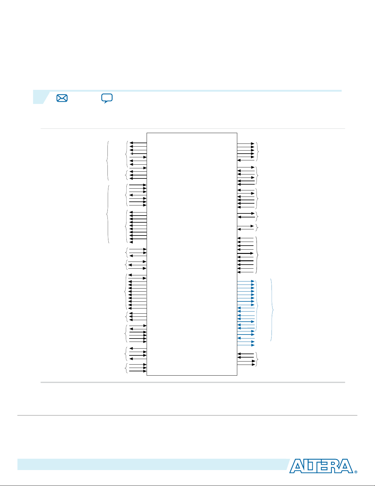
Figure 4-1: Avalon-ST Hard IP for PCI Express Top-Level Signals
©
trademarks of Altera Corporation and registered in the U.S. Patent and Trademark Office and in other countries. All other words and logos identified as
trademarks or service marks are the property of their respective holders as described at www.altera.com/common/legal.html. Altera warrants performance
of its semiconductor products to current specifications in accordance with Altera's standard warranty, but reserves the right to make changes to any
products and services at any time without notice. Altera assumes no responsibility or liability arising out of the application or use of any information,
product, or service described herein except as expressly agreed to in writing by Altera. Altera customers are advised to obtain the latest version of device
specifications before relying on any published information and before placing orders for products or services.
2014 Altera Corporation. All rights reserved. ALTERA, ARRIA, CYCLONE, ENPIRION, MAX, MEGACORE, NIOS, QUARTUS and STRATIX words and logos are
Subscribe
Send Feedback
ISO
9001:2008
Registered
Page 39

4-2
Arria V Hard IP for PCI Express with Avalon-ST Interface to the Application Layer
Related Information
• Features on page 1-2
• Qsys Design Flow on page 2-2
Arria V Hard IP for PCI Express with Avalon-ST Interface to the
Application Layer
Avalon‑ST RX Interface
Table 4-1: 64- or 128‑Bit Avalon-ST RX Datapath
The RX data signal can be 64 or 128 bits.
Signal Direction Description
2014.12.15
rx_st_data[<n>-1:0]
Output Receive data bus. Refer to figures following this table for the
mapping of the Transaction Layer’s TLP information to rx_st_
data and examples of the timing of this interface. Note that the
position of the first payload dword depends on whether the TLP
address is qword aligned. The mapping of message TLPs is the
same as the mapping of TLPs with 4-dword headers. When using
a 64-bit Avalon-ST bus, the width of rx_st_data is 64. When
using a 128-bit Avalon-ST bus, the width of rx_st_data is 128.
rx_st_sop
Output Indicates that this is the first cycle of the TLP when rx_st_valid
is asserted.
rx_st_eop Output Indicates that this is the last cycle of the TLP when rx_st_valid
is asserted.
rx_st_empty
Output Indicates the number of empty qwords in rx_st_data. Not used
when rx_st_data is 64 bits. Valid only when rx_st_eop is
asserted in 128-bit mode.
For 128-bit data, only bit 0 applies; this bit indicates whether the
upper qword contains data.
• 128-Bit interface:
Altera Corporation
• rx_st_empty = 0, rx_st_data[127:0]contains valid data
• rx_st_empty = 1, rx_st_data[63:0] contains valid data
Interfaces and Signal Descriptions
Send Feedback
Page 40

2014.12.15
Avalon‑ST RX Component Specific Signals
Signal Direction Description
rx_st_ready Input Indicates that the Application Layer is ready to accept data. The
Application Layer deasserts this signal to throttle the data stream.
If rx_st_ready is asserted by the Application Layer on cycle
<n> , then <n + > readyLatency > is a ready cycle, during which
the Transaction Layer may assert valid and transfer data.
The RX interface supports a readyLatency of 2 cycles.
rx_st_valid Output Clocks rx_st_data into the Application Layer. Deasserts within
2 clocks of rx_st_ready deassertion and reasserts within 2 clocks
of rx_st_ready assertion if more data is available to send.
4-3
rx_st_err
Output Indicates that there is an uncorrectable error correction coding
(ECC) error in the internal RX buffer. Active when ECC is
enabled. ECC is automatically enabled by the Quartus II
assembler. ECC corrects single-bit errors and detects double-bit
errors on a per byte basis.
When an uncorrectable ECC error is detected, rx_st_err is
asserted for at least 1 cycle while rx_st_valid is asserted.
Altera recommends resetting the Arria V Hard IP for PCI
Express when an uncorrectable double-bit ECC error is detected.
Related Information
Avalon Interface Specifications.
Avalon‑ST RX Component Specific Signals
Table 4-2: Avalon-ST RX Component Specific Signals
Signal Direction Description
rx_st_mask Input
The Application Layer asserts this signal to tell the Hard IP to
stop sending non-posted requests. This signal can be asserted at
any time. The total number of non-posted requests that can be
transferred to the Application Layer after rx_st_mask is asserted
is not more than 10.
Interfaces and Signal Descriptions
Send Feedback
Altera Corporation
Page 41

4-4
Avalon‑ST RX Component Specific Signals
Signal Direction Description
rx_st_bar[7:0] Output The decoded BAR bits for the TLP. Valid for MRd, MWr, IOWR, and
IORD TLPs. Ignored for the completion or message TLPs. Valid
during the cycle in which rx_st_sop is asserted.
Refer to 64-Bit Avalon-ST rx_st_data<n> Cycle Definitions for 4-
Dword Header TLPs with Non-Qword Addresses and 128-Bit
Avalon-ST rx_st_data<n> Cycle Definition for 3-Dword Header
TLPs with Qword Aligned Addresses for the timing of this signal
for 64- and 128-bit data, respectively.
The following encodings are defined for Endpoints:
• Bit 0: BAR 0
• Bit 1: BAR 1
• Bit 2: Bar 2
• Bit 3: Bar 3
• Bit 4: Bar 4
• Bit 5: Bar 5
• Bit 6: Expansion ROM
• Bit 7: Reserved
2014.12.15
The following encodings are defined for Root Ports:
• Bit 0: BAR 0
• Bit 1: BAR 1
• Bit 2: Primary Bus number
• Bit 3: Secondary Bus number
• Bit 4: Secondary Bus number to Subordinate Bus number
window
• Bit 5: I/O window
• Bit 6: Non-Prefetchable window
• Bit 7: Prefetchable window
Altera Corporation
Interfaces and Signal Descriptions
Send Feedback
Page 42

2014.12.15
Avalon‑ST RX Component Specific Signals
Signal Direction Description
rx_st_be[<n>-1:0] Output Byte enables corresponding to the rx_st_data. The byte enable
signals only apply to PCI Express Memory Write and I/O Write
TLP payload fields. When using 64-bit Avalon-ST bus, the width
of rx_st_be is 8 bits. When using 128-bit Avalon-ST bus, the
width of rx_st_be is 16 bits. This signal is optional. You can
derive the same information by decoding the FBE and LBE fields
in the TLP header. The byte enable bits correspond to data bytes
as follows:
• rx_st_data[127:120] = rx_st_be[15]
• rx_st_data[119:112] = rx_st_be[14]
• rx_st_data[111:104] = rx_st_be[13]
• rx_st_data[95:88] = rx_st_be[12]
• rx_st_data[87:80] = rx_st_be[11]
• rx_st_data[79:72] = rx_st_be[10]
• rx_st_data[71:64] = rx_st_be[9]
• rx_st_data[7:0] = rx_st_be[8]
• rx_st_data[63:56] = rx_st_be[7]
• rx_st_data[55:48] = rx_st_be[6]
• rx_st_data[47:40] = rx_st_be[5]
• rx_st_data[39:32] = rx_st_be[4]
• rx_st_data[31:24] = rx_st_be[3]
• rx_st_data[23:16] = rx_st_be[2]
• rx_st_data[15:8] = rx_st_be[1]
• rx_st_data[7:0] = rx_st_be[0]
4-5
rx_st_parity[<n>-1:0]
rx_bar_dec_func_
num[2:0]
For more information about the Avalon-ST protocol, refer to the Avalon Interface Specifications.
Related Information
Avalon Interface Specifications.
Interfaces and Signal Descriptions
This signal is deprecated.
Output
The IP core generates byte parity when you turn on Enable byte
parity ports on Avalon-ST interface on the System Settings tab
of the parameter editor. Each bit represents odd parity of the
associated byte of the rx_st_datarx_st_data bus. For example,
bit[0] corresponds to rx_st_data[7:0] rx_st_data[7:0], bit[1]
corresponds to rx_st_data[15:8].
Output Specifies which function the rx_st_bar signal applies to.
Altera Corporation
Send Feedback
Page 43

.
.
.
0x0
0x8
0x10
0x18
Header Addr = 0x4
64 bits
PCB Memory
Valid Data
Valid Data
4-6
Data Alignment and Timing for the 64‑Bit Avalon‑ST RX Interface
Data Alignment and Timing for the 64‑Bit Avalon‑ST RX Interface
To facilitate the interface to 64-bit memories, the Arria V Hard IP for PCI Express aligns data to the
qword or 64 bits by default. Consequently, if the header presents an address that is not qword aligned, the
Hard IP block shifts the data within the qword to achieve the correct alignment.
Qword alignment applies to all types of request TLPs with data, including the following TLPs:
• Memory writes
• Configuration writes
• I/O writes
The alignment of the request TLP depends on bit 2 of the request address. For completion TLPs with data,
alignment depends on bit 2 of the lower address field. This bit is always 0 (aligned to qword boundary)
for completion with data TLPs that are for configuration read or I/O read requests.
Figure 4-2: Qword Alignment
The following figure shows how an address that is not qword aligned, 0x4, is stored in memory. The byte
enables only qualify data that is being written. This means that the byte enables are undefined for 0x0–
0x3. This example corresponds to 64-Bit Avalon-ST rx_st_data<n> Cycle Definition for 3-Dword Header
TLPs with Non-Qword Aligned Address.
2014.12.15
Altera Corporation
The following table shows the byte ordering for header and data packets.
Table 4-3: Mapping Avalon-ST Packets to PCI Express TLPs
Packet TLP
Header0 pcie_hdr_byte0, pcie_hdr _byte1, pcie_hdr _byte2, pcie_hdr _byte3
Header1 pcie_hdr _byte4, pcie_hdr _byte5, pcie_hdr byte6, pcie_hdr _byte7
Header2 pcie_hdr _byte8, pcie_hdr _byte9, pcie_hdr _byte10, pcie_hdr _byte11
Header3 pcie_hdr _byte12, pcie_hdr _byte13, header_byte14, pcie_hdr _byte15
Data0 pcie_data_byte3, pcie_data_byte2, pcie_data_byte1, pcie_data_byte0
Interfaces and Signal Descriptions
Send Feedback
Page 44

pld_clk
rx_st_data[63:32]
rx_st_data[31:0]
rx_st_sop
rx_st_eop
rx_st_be[7:4]
rx_st_be[3:0]
Header1 Data0 Data2
Header0 Header2 Data1
F F
F
2014.12.15
Data Alignment and Timing for the 64‑Bit Avalon‑ST RX Interface
Packet TLP
4-7
Data1 pcie_data_byte7, pcie_data_byte6, pcie_data_byte5, pcie_data_byte4
Data2 pcie_data_byte11, pcie_data_byte10, pcie_data_byte9, pcie_data_byte8
Data<n> pcie_data_byte<4n+3>, pcie_data_byte<4n+2>, pcie_data_byte<4n+1>, pcie_data_
byte<n>
The following figure illustrates the mapping of Avalon-ST RX packets to PCI Express TLPs for a three
dword header with non-qword aligned addresses with a 64-bit bus. In this example, the byte address is
unaligned and ends with 0x4, causing the first data to correspond to rx_st_data[63:32] .
Note: The Avalon-ST protocol, as defined in Avalon Interface Specifications, is big endian, while the Hard
IP for PCI Express packs symbols into words in little endian format. Consequently, you cannot use
the standard data format adapters available in Qsys.
Figure 4-3: 64-Bit Avalon-ST rx_st_data<n> Cycle Definition for 3-Dword Header TLPs with Non-Qword
Aligned Address
Interfaces and Signal Descriptions
The following figure illustrates the mapping of Avalon-ST RX packets to PCI Express TLPs for a three
dword header with qword aligned addresses. Note that the byte enables indicate the first byte of data is
not valid and the last dword of data has a single valid byte.
Altera Corporation
Send Feedback
Page 45

clk
rx_st_data[63:32]
rx_st_data[31:0]
rx_st_sop
rx_st_eop
rx_st_be[7:4]
rx_st_be[3:0]
Header 1 Data1 Data3
Header 0 Header2 Data0 Data2
F 1
FE
pld_clk
rx_st_data[63:0]
rx_st_sop
rx_st_eop
rx_st_ready
rx_st_valid
000.010
.
CCCC0002CCCC0001 CC
.
CC
.
CC
.
CC
.
CC
.
CC
.
4-8
Data Alignment and Timing for the 64‑Bit Avalon‑ST RX Interface
Figure 4-4: 64-Bit Avalon-ST rx_st_data<n> Cycle Definition for 3-Dword Header TLPs with Qword
Aligned Address
In the following figure, rx_st_be[7:4] corresponds to rx_st_data[63:32]. rx_st_be[3:0]
corresponds to rx_st_data[31:0].
Figure 4-5: 64-Bit Application Layer Backpressures Transaction Layer
The following figure illustrates the timing of the RX interface when the Application Layer backpressures
the Arria V Hard IP for PCI Express by deasserting rx _st_ready. The rx_st_valid signal deasserts
within three cycles after rx_st_ready is deasserted. In this example, rx_st_valid is deasserted in the
next cycle. rx_st_data is held until the Application Layer is able to accept it.
2014.12.15
Altera Corporation
Interfaces and Signal Descriptions
Send Feedback
Page 46

pld_clk
rx_st_data[63:0]
rx_st_sop
rx_st_eop
rx_st_ready
rx_st_valid
C. C. C. C. CCCC0089002... C. C. C. C. C. C. C.
C.
C. C. C. C. C. C. C. C. C. C. C. C. C. C. C. C. C. C. C C
2014.12.15
Data Alignment and Timing for the 64‑Bit Avalon‑ST RX Interface
Figure 4-6: 4-Bit Avalon-ST Interface Back-to-Back Transmission
The following figure illustrates back-to-back transmission on the 64-bit Avalon-ST RX interface with no
idle cycles between the assertion of rx_st_eop and rx_st_sop.
Related Information
• Transaction Layer Packet (TLP) Header Formats on page 18-1
• Avalon Interface Specifications
4-9
Interfaces and Signal Descriptions
Send Feedback
Altera Corporation
Page 47

pld_clk
rx_st_valid
rx_st_data[127:96]
rx_st_data[95:64]
rx_st_data[63:32]
rx_st_data[31:0]
rx_st_bardec[7:0]
rx_st_sop
rx_st_eop
rx_st_empty
data3
header2 data2
header1 data1 data<n>
header0 data0 data<n-1>
01
4-10
Data Alignment and Timing for the 128‑Bit Avalon‑ST RX Interface
Data Alignment and Timing for the 128‑Bit Avalon‑ST RX Interface
Figure 4-7: 128-Bit Avalon-ST rx_st_data<n> Cycle Definition for 3-Dword Header TLPs with Qword
Aligned Addresses
The following figure shows the mapping of 128-bit Avalon-ST RX packets to PCI Express TLPs for TLPs
with a three dword header and qword aligned addresses. The assertion of rx_st_empty in a rx_st_eop
cycle, indicates valid data on the lower 64 bits of rx_st _data.
2014.12.15
Altera Corporation
Interfaces and Signal Descriptions
Send Feedback
Page 48

rx_st_valid
rx_st_data[127:96]
rx_st_data[95:64]
rx_st_data[63:32]
rx_st_data[31:0]
rx_st_sop
rx_st_eop
rx_st_empty
Data0
Data 4
Header 2
Data 3
Header 1 Data 2 Data (n)
Header 0 Data 1 Data (n-1)
pld_clk
pld_clk
rx_st_valid
rx_st_data[127:96]
rx_st_data[95:64]
rx_st_data[63:32]
rx_st_data[31:0]
rx_st_sop
rx_st_eop
rx_st_empty
Header 3 Data 2
Header 2 Data 1
Data n
Header 1 Data 0
Data n-1
Header 0
Data n-2
2014.12.15
Data Alignment and Timing for the 128‑Bit Avalon‑ST RX Interface
Figure 4-8: 128-Bit Avalon-ST rx_st_data<n> Cycle Definition for 3-Dword Header TLPs with nonQword Aligned Addresses
The following figure shows the mapping of 128-bit Avalon-ST RX packets to PCI Express TLPs for TLPs
with a 3 dword header and non-qword aligned addresses. In this case, bits[127:96] represent Data0
because address[2] in the TLP header is set. The assertion of rx_st_empty in a rx_st_eop cycle indicates
valid data on the lower 64 bits of rx_st_data.
4-11
Figure 4-9: 128-Bit Avalon-ST rx_st_data Cycle Definition for 4-Dword Header TLPs with non-Qword
Aligned Addresses
The following figure shows the mapping of 128-bit Avalon-ST RX packets to PCI Express TLPs for a four
dword header with non-qword aligned addresses. In this example, rx_st_empty is low because the data is
valid for all 128 bits in the rx_st_eop cycle.
Interfaces and Signal Descriptions
Send Feedback
Altera Corporation
Page 49

pld_clk
rx_st_valid
rx_st_data[127:96]
rx_st_data[95:64]
rx_st_data[63:32]
rx_st_data[31:0]
rx_st_sop
rx_st_eop
rx_st_empty
Header3 Data3 Data n
Header 2 Data 2 Data n-1
Header 1 Data 1 Data n-2
Header 0 Data 0 Data n-3
pld_clk
rx_st_data[127:0]
rx_st_sop
rx_st_eop
rx_st_empty
rx_st_ready
rx_st_valid
4562 . . . c19a . . . 0217b . . . 134c . . . 8945 . . .3458ce. . . 2457ce. . .000a7896c000bc34...
4-12
Data Alignment and Timing for the 128‑Bit Avalon‑ST RX Interface
Figure 4-10: 128-Bit Avalon-ST rx_st_data Cycle Definition for 4-Dword Header TLPs with Qword
Aligned Addresses
The following figure shows the mapping of 128-bit Avalon-ST RX packets to PCI Express TLPs for a four
dword header with qword aligned addresses. In this example, rx_st_empty is low because data is valid for
all 128-bits in the rx_st_eop cycle.
2014.12.15
Figure 4-11: 128-Bit Application Layer Backpressures Hard IP Transaction Layer for RX Transactions
The following figure illustrates the timing of the RX interface when the Application Layer backpressures
the Hard IP by deasserting rx_st_ready. The rx_st_valid signal deasserts within three cycles after
rx_st_ready is deasserted. In this example, rx_st_valid is deasserted in the next cycle. rx_st_data is
held until the Application Layer is able to accept it.
The following figure illustrates back-to-back transmission on the 128-bit Avalon-ST RX interface with no
idle cycles between the assertion of rx_st_eop and rx_st_sop.
Altera Corporation
Interfaces and Signal Descriptions
Send Feedback
Page 50

pld_clk
rx_st_data[127:0]
rx_st_sop
rx_st_eop
rx_st_empty
rx_st_ready
rx_st_valid
rx_st_err
BB ... BB ... BB ... BB ... BB ... BB ... BB ... BB ... BB ... BB ... BB ... BB ... ...BB
pld_clk
rx_st_data[127:0]
rx_st_sop
rx_st_eop
rx_st_empty
rx_st_ready
rx_st_valid
0000090 1C0020000F0000000100004 450AC89000012FE0D10004
2014.12.15
Avalon-ST TX Interface
Figure 4-12: 128-Bit Avalon-ST Interface Back-to-Back Transmission
The following figure illustrates back-to-back transmission on the 128-bit Avalon-ST RX interface with no
idle cycles between the assertion of rx_st_eop and rx_st_sop.
4-13
Figure 4-13: 128-Bit Packet Examples of rx_st_empty and Single-Cycle Packet
The following figure illustrates a two-cycle packet with valid data in the lower qword
(rx_st_data[63:0]) and a one-cycle packet where the rx_st_sop and rx_st_eop occur in the same
cycle.
For a complete description of the TLP packet header formats, refer to Appendix A, Transaction Layer
Packet (TLP) Header Formats.
Interfaces and Signal Descriptions
Avalon-ST TX Interface
The following table describes the signals that comprise the Avalon-ST TX Datapath. The TX data signal
can be 64 or 128.
Send Feedback
Altera Corporation
Page 51

4-14
Avalon-ST TX Interface
Table 4-4: 64- or 128‑Bit Avalon-ST TX Datapath
Signal Direction Description
2014.12.15
tx_st_data[<n>-1:0]
Input Data for transmission. Transmit data bus. Refer to the following
sections on data alignment for the 64- and 128-bit interfaces for
the mapping of TLP packets to tx_st_data and examples of the
timing of this interface. When using a 64-bit Avalon-ST bus, the
width of tx_st_d ata is 64. When using a 128-bit Avalon-ST
bus, the width of tx_st_data is 128 bits. The Application Layer
must provide a properly formatted TLP on the TX interface. The
mapping of message TLPs is the same as the mapping of Transac‐
tion Layer TLPs with 4 dword headers. The number of data
cycles must be correct for the length and address fields in the
header. Issuing a packet with an incorrect number of data cycles
results in the TX interface hanging and becoming unable to
accept further requests.
<n> = 64 or 128.
tx_st_sop
tx_st_eop
tx_st_ready Output Indicates that the Transaction Layer is ready to accept data for
Input Indicates first cycle of a TLP when asserted together with tx_st_
valid.
Input Indicates last cycle of a TLP when asserted together with tx_st_
valid.
transmission. The core deasserts this signal to throttle the data
stream. tx_st_ready may be asserted during reset. The Applica‐
tion Layer should wait at least 2 clock cycles after the reset is
released before issuing packets on the Avalon-ST TX interface.
The reset_status signal can also be used to monitor when the
IP core has come out of reset.
Altera Corporation
If tx_st_ready is asserted by the Transaction Layer on cycle
<n> , then <n + readyLatency> is a ready cycle, during which
the Application Layer may assert valid and transfer data.
When tx_st_ready, tx_st_valid and tx_st_data are
registered (the typical case), Altera recommends a readyLa-
tency of 2 cycles to facilitate timing closure; however, a
readyLatency of 1 cycle is possible. If no other delays are added
to the read-valid latency, the resulting delay corresponds to a
readyLatency of 2.
Interfaces and Signal Descriptions
Send Feedback
Page 52

2014.12.15
Avalon-ST TX Interface
Signal Direction Description
tx_st_valid Input Clocks tx_st_data to the core when tx_st_ready is also
asserted. Between tx_st_sop and tx_st_eop, tx_st_valid must
not be deasserted in the middle of a TLP except in response to
tx_st_ready deassertion. When tx_st_ready deasserts, this
signal must deassert within 1 or 2 clock cycles. When tx_st_
ready reasserts, and tx_st_data is in mid-TLP, this signal must
reassert within 2 cycles. The figure entitled64-Bit Transaction
Layer Backpressures the Application Layer illustrates the timing of
this signal.
To facilitate timing closure, Altera recommends that you register
both the tx_st_ready and tx_st_valid signals. If no other
delays are added to the ready-valid latency, the resulting delay
corresponds to a readyLatency of 2.
4-15
tx_st_empty[1:0]
tx_st_err
Input Indicates the number of qwords that are empty during cycles that
contain the end of a packet. When asserted, the empty dwords
are in the high-order bits. Valid only when tx_st_eop is asserted.
Not used when tx_st_data is 64 bits. For 128-bit data, only bit 0
applies and indicates whether the upper qword contains data.
For the 128-Bit interface:
• If tx_st_empty = 0, tx_st_data[127:0] contains valid data.
• If tx_st_empty = 1, tx_st_data[63:0] contains valid data.
Input Indicates an error on transmitted TLP. This signal is used to
nullify a packet. It should only be applied to posted and
completion TLPs with payload. To nullify a packet, assert this
signal for 1 cycle after the SOP and before the EOP. When a
packet is nullified, the following packet should not be transmitted
until the next clock cycle. tx_st_err is not available for packets
that are 1 or 2 cycles long.
Refer to the figure entitled 128-Bit Avalon-ST tx_st_data Cycle
Definition for 3-Dword Header TLP with non-Qword Aligned
Address for a timing diagram that illustrates the use of the error
signal. Note that it must be asserted while the valid signal is
asserted.
tx_cred_
datafccp[11:0]
tx_cred_
datafcnp[11:0]
Interfaces and Signal Descriptions
Send Feedback
Component Specific Signals
Output Data credit limit for the received FC completions. Each credit is
16 bytes.
Output Data credit limit for the non-posted requests. Each credit is 16
bytes.
Altera Corporation
Page 53

4-16
Avalon-ST TX Interface
Signal Direction Description
2014.12.15
tx_cred_datafcp[11:0]
tx_cred_
fchipcons[5:0]
Output Data credit limit for the FC posted writes. Each credit is 16 bytes.
Output Asserted for 1 cycle each time the Hard IP consumes a credit.
These credits are from messages that the Hard IP for PCIe
generates for the following reasons:
• To respond to memory read requests
• To send error messages
This signal is not asserted when an Application Layer credit is
consumed. The Application Layer must keep track of its own
consumed credits. To calculate the total credits consumed, the
Application Layer must add its own credits consumed to those
consumed by the Hard IP for PCIe. The credit signals are valid
after dlup (data link up) is asserted.
The 6 bits of this vector correspond to the following 6 types of
credit types:
• [5]: posted headers
• [4]: posted data
• [3]: non-posted header
• [2]: non-posted data
• [1]: completion header
• [0]: completion data
tx_cred_
fcinfinite[5:0]
tx_cred_hdrfccp[7:0]
tx_cred_hdrfcnp[7:0]
During a single cycle, the IP core can consume either a single
header credit or both a header and a data credit.
Output When asserted, indicates that the corresponding credit type has
infinite credits available and does not need to calculate credit
limits. The 6 bits of this vector correspond to the following 6
types of credit types:
• [5]: posted headers
• [4]: posted data
• [3]: non-posted header
• [2]: non-posted data
• [1]: completion header
• [0]: completion data
Output Header credit limit for the FC completions. Each credit is 20
bytes.
O Header limit for the non-posted requests. Each credit is 20 bytes.
Altera Corporation
Interfaces and Signal Descriptions
Send Feedback
Page 54

2014.12.15
Avalon-ST Packets to PCI Express TLPs
Signal Direction Description
4-17
tx_cred_hdrfcp[7:0]
ko_cpl_spc_
header[7:0]
ko_cpl_spc_data[11:0]
O Header credit limit for the FC posted writes. Each credit is 20
Output The Application Layer can use this signal to build circuitry to
Output The Application Layer can use this signal to build circuitry to
Avalon-ST Packets to PCI Express TLPs
The following figures illustrate the mappings between Avalon-ST packets and PCI Express TLPs. These
mappings apply to all types of TLPs, including posted, non-posted, and completion TLPs. Message TLPs
use the mappings shown for four dword headers. TLP data is always address-aligned on the Avalon-ST
interface whether or not the lower dwords of the header contains a valid address, as may be the case with
TLP type (message request with data payload).
bytes.
prevent RX buffer overflow for completion headers. Endpoints
must advertise infinite space for completion headers; however,
RX buffer space is finite. ko_cpl_spc_header is a static signal
that indicates the total number of completion headers that can be
stored in the RX buffer.
prevent RX buffer overflow for completion data. Endpoints must
advertise infinite space for completion data; however, RX buffer
space is finite. ko_cpl_spc_data is a static signal that reflects the
total number of 16 byte completion data units that can be stored
in the completion RX buffer.
For additional information about TLP packet headers, refer to Appendix A, Transaction Layer Packet
(TLP) Header Formats and Section 2.2.1 Common Packet Header Fields in the PCI Express Base Specifica‐
tion .
Related Information
PCI Express Base Specification Revision 2.1 or 3.0
Interfaces and Signal Descriptions
Send Feedback
Altera Corporation
Page 55

pld_clk
tx_st_data[63:32]
tx_st_data[31:0]
tx_st_sop
tx_st_eop
Header1 Data0 Data2
Header0 Header2 Data1
pld_clk
tx_st_data[63:32]
tx_st_data[31:0]
tx_st_sop
tx_st_eop
Header1 Header3 Data1
Header0 Header2 Data0
4-18
Data Alignment and Timing for the 64‑Bit Avalon‑ST TX Interface
Data Alignment and Timing for the 64‑Bit Avalon‑ST TX Interface
Figure 4-14:
The following figure illustrates the mapping between Avalon-ST TX packets and PCI Express TLPs for
three dword header TLPs with non-qword aligned addresses on a 64-bit bus.
Figure 4-15: 64-Bit Avalon-ST tx_st_data Cycle Definition for 3-Dword Header TLP with Non-Qword
Aligned Address
This figure illustrates the storage of non-qword aligned data.) Non-qword aligned address occur when
address[2] is set. When address[2] is set, tx_st_data[63:32]contains Data0 and tx_st_data[31:0]
contains dword header2. In this figure, the headers are formed by the following bytes:
2014.12.15
H0 ={pcie_hdr_byte0, pcie_hdr _byte1, pcie_hdr _byte2, pcie_hdr _byte3}
H1 = {pcie_hdr_byte4, pcie_hdr _byte5, header pcie_hdr byte6, pcie_hdr _byte7}
H2 = {pcie_hdr _byte8, pcie_hdr _byte9, pcie_hdr _byte10, pcie_hdr _byte11}
Data0 = {pcie_data_byte3, pcie_data_byte2, pcie_data_byte1, pcie_data_byte0}
Data1 = {pcie_data_byte7, pcie_data_byte6, pcie_data_byte5, pcie_data_byte4}
Data2 = {pcie_data_byte11, pcie_data_byte10, pcie_data_byte9, pcie_data_byte8}
The following figure illustrates the mapping between Avalon-ST TX packets and PCI Express TLPs for a
four dword header with qword aligned addresses on a 64-bit bus
Figure 4-16: 64-Bit Avalon-ST tx_st_data Cycle Definition for 4-Dword TLP with Qword Aligned
Address
In this figure, the headers are formed by the following bytes.
Altera Corporation
H0 = {pcie_hdr_byte0, pcie_hdr _byte1, pcie_hdr _byte2, pcie_hdr _byte3}
H1 = {pcie_hdr _byte4, pcie_hdr _byte5, pcie_hdr byte6, pcie_hdr _byte7}
H2 = {pcie_hdr _byte8, pcie_hdr _byte9, pcie_hdr _byte10, pcie_hdr _byte11}
H3 = pcie_hdr _byte12, pcie_hdr _byte13, header_byte14, pcie_hdr _byte15}, 4 dword
header only
Interfaces and Signal Descriptions
Send Feedback
Page 56

pld_clk
tx_st_data[63:32]
tx_st_data[31:0]
tx_st_sop
tx_st_eop
Header 1 Header3 Data0 Data2
Header 0 Header2 Data1
coreclkout
tx_st_sop
tx_st_eop
tx_st_ready
tx_st_valid
tx_st_err
tx_st_data[63:0] . . . . . . . . . .
readyLatency
00. . 00 ... BB... BB ... BBBB0306BBB0305 BB... BB.. BB ... BB ... BB ... BB ... BB... .
2014.12.15
Data Alignment and Timing for the 64‑Bit Avalon‑ST TX Interface
Data0 = {pcie_data_byte3, pcie_data_byte2, pcie_data_byte1, pcie_data_byte0}
Data1 = {pcie_data_byte7, pcie_data_byte6, pcie_data_byte5, pcie_data_byte4}
4-19
Figure 4-17: 64-Bit Avalon-ST tx_st_data Cycle Definition for TLP 4-Dword Header with Non-Qword
Aligned Address
Figure 4-18: 64-Bit Transaction Layer Backpressures the Application Layer
The following figure illustrates the timing of the TX interface when the Arria V Hard IP for PCI Express
pauses transmission by the Application Layer by deasserting tx_st_ready. Because the readyLatency is
two cycles, the Application Layer deasserts tx_st_valid after two cycles and holds tx_st_data until two
cycles after tx_st_ready is asserted.
Interfaces and Signal Descriptions
Send Feedback
Altera Corporation
Page 57

coreclkout
tx_st_sop
tx_st_eop
tx_st_ready
tx_st_valid
tx_st_err
tx_st_data[63:0] 01 ... 00 ... BB ... BB ... BB ... BB ... B ... ... BB ... 01 ... 00 ... CC ... CC ... CC ... CC ... CC ... CC ...
Data3
Header2 Data 2
Header1 Data1 Data(n)
Header0 Data0 Data(n-1)
pld_clk
tx_st_valid
tx_st_data[127:96]
tx_st_data[95:64]
tx_st_data[63:32]
tx_st_data[31:0]
tx_st_sop
tx_st_eop
tx_st_empty
4-20
Data Alignment and Timing for the 128‑Bit Avalon‑ST TX Interface
Figure 4-19: 64-Bit Back-to-Back Transmission on the TX Interface
The following figure illustrates back-to-back transmission of 64-bit packets with no idle cycles between
the assertion of tx_st_eop and tx_st_sop.
Data Alignment and Timing for the 128‑Bit Avalon‑ST TX Interface
2014.12.15
Figure 4-20: 128-Bit Avalon-ST tx_st_data Cycle Definition for 3-Dword Header TLP with Qword
Aligned Address
The following figure shows the mapping of 128-bit Avalon-ST TX packets to PCI Express TLPs for a three
dword header with qword aligned addresses. Assertion of tx_st_empty in an rx_st_eop cycle indicates
valid data in the lower 64 bits of tx_st_data.
Altera Corporation
Interfaces and Signal Descriptions
Send Feedback
Page 58

pld_clk
tx_st_valid
tx_st_data[127:96]
tx_st_data[95:64]
tx_st_data[63:32]
tx_st_data[31:0]
tx_st_sop
tx_st_err
tx_st_eop
tx_st_empty
Data0 Data 4
Header 2
Data 3
Header 1 Data 2 Data (n)
Header 0 Data 1 Data (n-1)
pld_clk
tx_st_data[127:96]
tx_st_data[95:64]
tx_st_data[63:32]
tx_st_data[31:0]
tx_st_sop
tx_st_eop
tx_st_empty
Header 3 Data 3
Header 2 Data 2
Header 1 Data 1
Header 0 Data 0 Data 4
2014.12.15
Data Alignment and Timing for the 128‑Bit Avalon‑ST TX Interface
4-21
Figure 4-21: 128-Bit Avalon-ST tx_st_data Cycle Definition for 3-Dword Header TLP with non-Qword
Aligned Address
The following figure shows the mapping of 128-bit Avalon-ST TX packets to PCI Express TLPs for a 3
dword header with non-qword aligned addresses. It also shows tx_st_err assertion.
Figure 4-22: 128-Bit Avalon-ST tx_st_data Cycle Definition for 4-Dword Header TLP with Qword
Aligned Address
Interfaces and Signal Descriptions
Figure 4-23: 128-Bit Avalon-ST tx_st_data Cycle Definition for 4-Dword Header TLP with non-Qword
Aligned Address
The following figure shows the mapping of 128-bit Avalon-ST TX packets to PCI Express TLPs for a four
dword header TLP with non-qword aligned addresses. In this example, tx_st_empty is low because the
data ends in the upper 64 bits of tx_st_data.
Send Feedback
Altera Corporation
Page 59

Header 3 Data 2
Header 2 Data 1
Data n
Header 1 Data 0
Data n-1
Header 0
Data n-2
pld_clk
tx_st_valid
tx_st_data[127:96]
tx_st_data[95:64]
tx_st_data[63:32]
tx_st_data[31:0]
tx_st_sop
tx_st_eop
tx_st_empty
pld_clk
tx_st_data[127:0]
tx_st_sop
tx_st_eop
tx_st_empty
tx_st_ready
tx_st_valid
tx_st_err
.. . . . . . . . . . . . . . . . . . . . . . . . . . . . . . . . . . . . . . .
4-22
Data Alignment and Timing for the 128‑Bit Avalon‑ST TX Interface
Figure 4-24: 128-Bit Back-to-Back Transmission on the Avalon-ST TX Interface
The following figure illustrates back-to-back transmission of 128-bit packets with idle dead cycles between
the assertion of tx_st_eop and tx_st_sop.
2014.12.15
Altera Corporation
Figure 4-25: 128-Bit Hard IP Backpressures the Application Layer for TX Transactions
The following figure illustrates the timing of the TX interface when the Arria V Hard IP for PCI Express
pauses the Application Layer by deasserting tx_st_ready. Because the readyLatency is two cycles, the
Application Layer deasserts tx_st_valid after two cycles and holds tx_st_data until two cycles after
tx_st_ready is reasserted
Interfaces and Signal Descriptions
Send Feedback
Page 60

pld_clk
tx_st_data[127:0]
tx_st_sop
tx_st_eop
tx_st_empty
tx_st_ready
tx_st_valid
tx_st_err
000 CC... CC... CC... CC... CC... CC... CC... CC... CC... CC... CC...
2014.12.15
Root Port Mode Configuration Requests
If your Application Layer implements ECRC forwarding, it should not apply ECRC forwarding to
Configuration Type 0 packets that it issues on the Avalon-ST interface. There should be no ECRC
appended to the TLP, and the TD bit in the TLP header should be set to 0. These packets are processed
internally by the Hard IP block and are not transmitted on the PCI Express link.
Root Port Mode Configuration Requests
4-23
To ensure proper operation when sending Configuration Type 0 transactions in Root Port mode, the
application should wait for the Configuration Type 0 transaction to be transferred to the Hard IP for PCI
Express Configuration Space before issuing another packet on the Avalon-ST TX port. You can do this by
waiting for the core to respond with a completion on the Avalon-ST RX port before issuing the next
Configuration Type 0 transaction.
Interfaces and Signal Descriptions
Send Feedback
Altera Corporation
Page 61

4-24
Clock Signals
Clock Signals
Table 4-5: Clock Signals
Signal Direction Description
2014.12.15
refclk
pld_clk
coreclkout
Input Reference clock for the IP core. It must have the frequency
specified under the System Settings heading in the parameter
editor. This is a dedicated free running input clock to the
dedicated REFCLK pin.
If your design meets the following criteria:
• Enables CvP
• Includes an additional transceiver PHY connected to the same
Transceiver Reconfiguration Controller
then you must connect refclk to the mgmt_clk_clk signal of the
Transceiver Reconfiguration Controller and the additional
transceiver PHY. In addition, if your design includes more than
one Transceiver Reconfiguration Controller on the same side of
the FPGA, they all must share the mgmt_clk_clk signal.
Input Clocks the Application Layer. You can drive this clock with
coreclkout_hip. If you drive pld_clk with another clock
source, it must be equal to or faster than coreclkout_hip.
Output This is a fixed frequency clock used by the Data Link and
Transaction Layers. To meet PCI Express link bandwidth
constraints, this clock has minimum frequency requirements as
listed in Application Layer Clock Frequency for All Combination
of Link Width, Data Rate and Application Layer Interface Width
in the Reset and Clocks chapter .
Related Information
Clocks on page 6-5
Reset Signals
Refer to Reset and Clocks for more information about the reset sequence and a block diagram of the reset
logic.
Altera Corporation
Interfaces and Signal Descriptions
Send Feedback
Page 62

2014.12.15
Table 4-6: Reset Signals
Signal Direction Description
Reset Signals
4-25
npor
reset_status
pin_perst
Input Active low reset signal. In the Altera hardware example designs,
npor is the OR of pin_perst and local_rstn coming from the
software Application Layer. If you do not drive a soft reset signal
from the Application Layer, this signal must be derived from
pin_perst. You cannot disable this signal. Resets the entire IP
Core and transceiver. Asynchronous.
In systems that use the hard reset controller, this signal is edge,
not level sensitive; consequently, you cannot use a low value on
this signal to hold custom logic in reset. For more information
about the hard and soft reset controllers, refer to the Reset and
Clocks chapter.
Output Active high reset status signal. When asserted, this signal
indicates that the Hard IP clock is in reset. The reset_status
signal is synchronous to the pld_clk clock and is deasserted only
when the npor is deasserted and the Hard IP for PCI Express is
not in reset (reset_status_hip = 0). You should use reset_
status to drive the reset of your application. This reset is used
for the Hard IP for PCI Express IP Core with the Avalon-ST
interface.
Input Active low reset from the PCIe reset pin of the device. pin_perst
resets the datapath and control registers. This signal is required
for Configuration via Protocol (CvP). For more information
about CvP refer to Configuration via Protocol (CvP).
Interfaces and Signal Descriptions
Send Feedback
Arria V have 1 or 2 instances of the Hard IP for PCI Express.
Each instance has its own pin_perst signal. You must connect
the pin_perst of each Hard IP instance to the corresponding
nPERST pin of the device. These pins have the following locations:
• nPERSTL0: bottom left Hard IP and CvP blocks
• nPERSTL1: top left Hard IP block
For example, if you are using the Hard IP instance in the bottom
left corner of the device, you must connect pin_perst to
nPERSL0.
For maximum use of the Arria V device, Altera recommends that
you use the bottom left Hard IP first. This is the only location
that supports CvP over a PCIe link.
Refer to the appropriate device pinout for correct pin assignment
for more detailed information about these pins. The PCI Express
Card Electromechanical Specification 2.0 specifies this pin
requires 3.3 V. You can drive this 3.3V signal to the nPERST*
Altera Corporation
Page 63

npor
IO_POF_Load
PCIe_LinkTraining_Enumeration
dl_ltssm[4:0]
detect
detect.active polling.active
L0
4-26
Hard IP Status
Signal Direction Description
2014.12.15
even if the V
VCCPGM
of the bank is not 3.3V if the following 2
conditions are met:
• The input signal meets the VIH and VIL specification for
LVTTL.
• The input signal meets the overshoot specification for 100°C
operation as specified by the “Maximum Allowed Overshoot
and Undershoot Voltage” in the Device Datasheet for Arria V
Devices.
Figure 4-26: Reset and Link Training Timing Relationships
The following figure illustrates the timing relationship between npor and the LTSSM L0 state.
Note: To meet the 100 ms system configuration time, you must use the fast passive parallel configuration
scheme with and a 32-bit data width (FPP x32).
Related Information
• Reset and Clocks on page 6-1
• PCI Express Card Electromechanical Specification 2.0
• Device Datasheet for Arria V Devices
Hard IP Status
Refer to Reset and Clocks for more information about the reset sequence and a block diagram of the reset
logic.
Table 4-7: Status and Link Training Signals
Signal Direction Description
serdes_pll_locked
Output When asserted, indicates that the PLL that generates the
coreclkout_hip clock signal is locked. In pipe simulation mode
this signal is always asserted.
Altera Corporation
Interfaces and Signal Descriptions
Send Feedback
Page 64

2014.12.15
Signal Direction Description
Hard IP Status
4-27
pld_core_ready
pld_clk_inuse
dlup
dlup_exit
Input When asserted, indicates that the Application Layer is ready for
operation and is providing a stable clock to the pld_clk input. If
the coreclkout_hip Hard IP output clock is sourcing the pld_
clk Hard IP input, this input can be connected to the serdes_
pll_locked output.
Output When asserted, indicates that the Hard IP Transaction Layer is
using the pld_clk as its clock and is ready for operation with the
Application Layer. For reliable operation, hold the Application
Layer in reset until pld_clk_inuse is asserted.
Output When asserted, indicates that the Hard IP block is in the Data
Link Control and Management State Machine (DLCMSM) DL_
Up state.
Output This signal is asserted low for one pld_clk cycle when the IP
core exits the DLCMSM DL_Up state, indicating that the Data
Link Layer has lost communication with the other end of the
PCIe link and left the Up state. When this pulse is asserted, the
Application Layer should generate an internal reset signal that is
asserted for at least 32 cycles.
ev128ns
ev1us
hotrst_exit
Output Asserted every 128 ns to create a time base aligned activity.
Output Asserted every 1µs to create a time base aligned activity.
Output Hot reset exit. This signal is asserted for 1 clock cycle when the
LTSSM exits the hot reset state. This signal should cause the
Application Layer to be reset. This signal is active low. When this
pulse is asserted, the Application Layer should generate an
internal reset signal that is asserted for at least 32 cycles.
l2_exit
Output L2 exit. This signal is active low and otherwise remains high. It is
asserted for one cycle (changing value from 1 to 0 and back to 1)
after the LTSSM transitions from l2.idle to detect. When this
pulse is asserted, the Application Layer should generate an
internal reset signal that is asserted for at least 32 cycles.
lane_act[3:0] Output Lane Active Mode: This signal indicates the number of lanes that
configured during link training. The following encodings are
defined:
• 4'b0001: 1 lane
• 4'b0010: 2 lanes
• 4'b0100: 4 lanes
• 4'b1000: 8 lanes
Interfaces and Signal Descriptions
Send Feedback
Altera Corporation
Page 65

4-28
Hard IP Status
Signal Direction Description
2014.12.15
currentspeed[1:0]
ltssmstate[4:0]
Output Indicates the current speed of the PCIe link. The following
encodings are defined:
• 2b’00: Undefined
• 2b’01: Gen1
• 2b’10: Gen2
• 2b’11: Gen3
Output LTSSM state: The LTSSM state machine encoding defines the
following states:
• 00000: Detect.Quiet
• 00001: Detect.Active
• 00010: Polling.Active
• 00011: Polling.Compliance
• 00100: Polling.Configuration
• 00101: Polling.Speed
• 00110: config.Linkwidthstart
• 00111: Config.Linkaccept
• 01000: Config.Lanenumaccept
• 01001: Config.Lanenumwait
• 01010: Config.Complete
• 01011: Config.Idle
• 01100: Recovery.Rcvlock
• 01101: Recovery.Rcvconfig
• 01110: Recovery.Idle
• 01111: L0
• 10000: Disable
• 10001: Loopback.Entry
• 10010: Loopback.Active
• 10011: Loopback.Exit
• 10100: Hot.Reset
• 10101: LOs
• 11001: L2.transmit.Wake
• 11010: Speed.Recovery
• 11011: Recovery.Equalization, Phase 0
• 11100: Recovery.Equalization, Phase 1
• 11101: Recovery.Equalization, Phase 2
• 11110: recovery.Equalization, Phase 3
Related Information
PCI Express Card Electromechanical Specification 2.0
Altera Corporation
Interfaces and Signal Descriptions
Send Feedback
Page 66

2014.12.15
Error Signals
The following table describes the ECC error signals. These signals are all valid for one clock cycle. They
are synchronous to coreclkout_hip.
ECC for the RX and retry buffers is implemented with MRAM. These error signals are flags. If a specific
location of MRAM has errors, as long as that data is in the ECC decoder, the flag indicates the error.
When a correctable ECC error occurs, the Arria V Hard IP for PCI Express recovers without any loss of
information. No Application Layer intervention is required. In the case of uncorrectable ECC error,
Altera recommends that you reset the core.
The Avalon-ST rx_st_err indicates an uncorrectable error in the RX buffer. This signal is described in
64- or 128-Bit Avalon-ST RX Datapath in the Avalon-ST RX Interface description.
Table 4-8: Error Signals
derr_cor_ext_rcv0 Output Indicates a corrected error in the RX buffer. This signal is for
Signal I/O Description
debug only. It is not valid until the RX buffer is filled with data.
This is a pulse, not a level, signal. Internally, the pulse is
generated with the 500 MHz clock. A pulse extender extends the
signal so that the FPGA fabric running at 250 MHz can capture
it. Because the error was corrected by the IP core, no Application
Layer intervention is required.
(1)
Error Signals
4-29
derr_rpl Output Indicates an uncorrectable error in the retry buffer. This signal is
for debug only.
derr_cor_ext_rpl0 Output Indicates a corrected ECC error in the retry buffer. This signal is
(1)
for debug only. Because the error was corrected by the IP core,
no Application Layer intervention is required.
(1)
Notes:
1. Debug signals are not rigorously verified and should only be used to observe behavior. Debug signals
should not be used to drive logic custom logic.
Related Information
Avalon-ST RX Interface on page 4-2
ECRC Forwarding
On the Avalon-ST interface, the ECRC field follows the same alignment rules as payload data. For packets
with payload, the ECRC is appended to the data as an extra dword of payload. For packets without
payload, the ECRC field follows the address alignment as if it were a one dword payload. The position of
the ECRC data for data depends on the address alignment. For packets with no payload data, the ECRC
position corresponds to the position of Data0.
Interfaces and Signal Descriptions
Send Feedback
Altera Corporation
Page 67

4-30
Interrupts for Endpoints
Interrupts for Endpoints
Refer to Interrupts for detailed information about all interrupt mechanisms.
Table 4-9: Interrupt Signals for Endpoints
Signal Direction Description
2014.12.15
app_msi_req
app_msi_ack
app_msi_tc[2:0]
app_msi_num[4:0]
app_msi_func[2:0]
app_int_sts[7:0]
Input Application Layer MSI request. Assertion causes an MSI posted
write TLP to be generated based on the MSI configuration
register values and the app_msi_tc and app_msi_num input
ports.
Output Application Layer MSI acknowledge. This signal acknowledges
the Application Layer's request for an MSI interrupt.
Input Application Layer MSI traffic class. This signal indicates the
traffic class used to send the MSI (unlike INTX interrupts, any
traffic class can be used to send MSIs).
Input MSI number of the Application Layer. This signal provides the
low order message data bits to be sent in the message data field of
MSI messages requested by app_msi_req. Only bits that are
enabled by the MSI Message Control register apply.
Input Indicates which function is asserting an interrupt with 0
corresponding to function 0, 1 corresponding to function 1, and
so on.
Input Level active interrupt signal. Bit 0 corresponds to function 0, and
so on. Drives the INTx line for that function. The core maps this
status to INT A/B/C/D according to the function Interrupt_Pin
register. The core internally wire-ORs the INT requests from all
sources, and generates INT messages on the rising/falling edges
of the wire-ORed result. The core logs the app_int_sts[7:0]
status in the function PCI Status register.
Related Information
• Legacy Interrupts on page 7-6
• Interrupts for Endpoints on page 7-1
Altera Corporation
Interfaces and Signal Descriptions
Send Feedback
Page 68

2014.12.15
Interrupts for Root Ports
Table 4-10: Interrupt Signals for Root Ports
Signal Direction Description
Interrupts for Root Ports
4-31
int_status[3:0]
Output These signals drive legacy interrupts to the Application Layer as
follows:
• int_status[0]: interrupt signal A
• int_status[1]: interrupt signal B
• int_status[2]: interrupt signal C
• int_status[3]: interrupt signal D
aer_msi_num[4:0] Input Advanced error reporting (AER) MSI number. Provides the low-
order message data bits to be sent in the message data field of the
MSI messages associated with the AER capability structure. Only
bits that are enabled by the MSI Message Control register are
used. For Root Ports only.
pex_msi_num[4:0] Input Power management MSI number. This signal provides the low-
order message data bits to be sent in the message data field of
MSI messages associated with the PCI Express capability
structure. Only bits that are enabled by the MSI Message Control
register are used. For Root Ports only.
serr_out
Output System Error: This signal only applies to Root Port designs that
report each system error detected, assuming the proper enabling
bits are asserted in the Root Control and Device Control
registers. If enabled, serr_out is asserted for a single clock cycle
when a system error occurs. System errors are described in the
PCI Express Base Specification 2.1 or 3.0 in the Root Control
register.
Related Information
PCI Express Base Specification 2.1 or 3.0
Completion Side Band Signals
The following table describes the signals that comprise the completion side band signals for the AvalonST interface. The Arria V Hard IP for PCI Express provides a completion error interface that the Applica‐
tion Layer can use to report errors, such as programming model errors. When the Application Layer
detects an error, it can assert the appropriate cpl_err bit to indicate what kind of error to log. If separate
requests result in two errors, both are logged. The Hard IP sets the appropriate status bits for the errors in
the Configuration Space, and automatically sends error messages in accordance with the PCI Express Base
Specification. Note that the Application Layer is responsible for sending the completion with the
Interfaces and Signal Descriptions
Send Feedback
Altera Corporation
Page 69

4-32
Completion Side Band Signals
appropriate completion status value for non-posted requests. Refer to Error Handling for information on
errors that are automatically detected and handled by the Hard IP.
For a description of the completion rules, the completion header format, and completion status field
values, refer to Section 2.2.9 of the PCI Express Base Specification.
Table 4-11: Completion Signals for the Avalon-ST Interface
2014.12.15
Signal Directi
cpl_err[6:0]
Description
on
Input Completion error. This signal reports completion errors to the
Configuration Space. When an error occurs, the appropriate signal is
asserted for one cycle.
• cpl_err[0]: Completion timeout error with recovery. This signal
should be asserted when a master-like interface has performed a
non-posted request that never receives a corresponding
completion transaction after the 50 ms timeout period when the
error is correctable. The Hard IP automatically generates an
advisory error message that is sent to the Root Complex.
• cpl_err[1]: Completion timeout error without recovery. This
signal should be asserted when a master-like interface has
performed a non-posted request that never receives a
corresponding completion transaction after the 50 ms time-out
period when the error is not correctable. The Hard IP automati‐
cally generates a non-advisory error message that is sent to the
Root Complex.
• cpl_err[2]: Completer abort error. The Application Layer asserts
this signal to respond to a non-posted request with a Completer
Abort (CA) completion. The Application Layer generates and
sends a completion packet with Completer Abort (CA) status to
the requestor and then asserts this error signal to the Hard IP. The
Hard IP automatically sets the error status bits in the Configura‐
tion Space register and sends error messages in accordance with
the PCI Express Base Specification.
• cpl_err[3]: Unexpected completion error. This signal must be
asserted when an Application Layer master block detects an
unexpected completion transaction. Many cases of unexpected
completions are detected and reported internally by the Transac‐
tion Layer. For a list of these cases, refer to Transaction Layer
Errors.
Altera Corporation
Interfaces and Signal Descriptions
Send Feedback
Page 70

2014.12.15
Completion Side Band Signals
4-33
Signal Directi
on
Description
• cpl_err[4]: Unsupported Request (UR) error for posted TLP.
The Application Layer asserts this signal to treat a posted request
as an Unsupported Request. The Hard IP automatically sets the
error status bits in the Configuration Space register and sends
error messages in accordance with the PCI Express Base Specifica‐
tion. Many cases of Unsupported Requests are detected and
reported internally by the Transaction Layer. For a list of these
cases, refer to Transaction Layer Errors.
• cpl_err[5]: Unsupported Request error for non-posted TLP. The
Application Layer asserts this signal to respond to a non-posted
request with an Request (UR) completion. In this case, the
Application Layer sends a completion packet with the
Unsupported Request status back to the requestor, and asserts this
error signal. The Hard IP automatically sets the error status bits in
the Configuration Space Register and sends error messages in
accordance with the PCI Express Base Specification. Many cases of
Unsupported Requests are detected and reported internally by the
Transaction Layer. For a list of these cases, refer to Transaction
Layer Errors.
• cpl_err[6]: Log header. If header logging is required, this bit
must be set in the every cycle in which any of cpl_err[2], cpl_
err[3], cpl_err[4], or cpl_err[5]is set. The Application Layer
presents the header to the Hard IP by writing the following values
to the following 4 registers using LMI before asserting cpl_
err[6]:. The Application Layer presents the header to the Hard IP
by writing the following values to the following 4 registers using
LMI before asserting cpl_err[6]:
cpl_pending[7:0]
cpl_err_func[2:0]
Interfaces and Signal Descriptions
Send Feedback
Input
• lmi_addr: 12'h81C, lmi_din: err_desc_func0[127:96]
• lmi_addr: 12'h820, lmi_din: err_desc_func0[95:64]
• lmi_addr: 12'h824, lmi_din: err_desc_func0[63:32]
• lmi_addr: 12'h828, lmi_din: err_desc_func0[31:0]
Completion pending. The Application Layer must assert this signal
when a master block is waiting for completion, for example, when a
transaction is pending. This is a level sensitive input. A bit is provided
for each function, where bit 0 corresponds to function 0, and so on.
Specifies which function is requesting the cpl_err. Must be asserted
when cpl_err asserts. Due to clock-domain synchronization
circuitry, cpl_err is limited to at most 1 assertion every 8 pld_clk
cycles. Whenever cpl_err is asserted, cpl_err_func[2:0] should be
updated in the same cycle.
Altera Corporation
Page 71

4-34
Transaction Layer Configuration Space Signals
Related Information
Transaction Layer Errors on page 8-3
Transaction Layer Configuration Space Signals
Table 4-12: Configuration Space Signals
These signals are not available if Configuration Space Bypass mode is enabled.
Signal Direction Description
2014.12.15
tl_cfg_add[6:0]
tl_cfg_ctl[31:0]
tl_cfg_ctl_wr
tl_cfg_sts[122:0]
0utput Address of the register that has been updated. This signal is an
index indicating which Configuration Space register information is
being driven onto tl_cfg_ctl. The indexing is defined in
Multiplexed Configuration Register Information Available on tl_
cfg_ctl. The index increments every 8coreclkout cycle. The
index increments every 8 coreclkout cycles. The index consists of
the following 2 fields:
• [6:4] - indicates the function number whose information is
being presented on tl_cfg_ctl
• [3:0] - the tl_cfg_ctltl_cfg_ctl multiplexor index
0utput The signal is multiplexed and contains the contents of the
Configuration Space registers. The indexing is defined in
Multiplexed Configuration Register Information Available on tl_
cfg_ctl.
0utput
Write signal. This signal toggles when tl_cfg_ctl has been
updated (every 8 coreclkout cycles). The toggle edge marks
where the tl_cfg_ctl data changes. You can use this edge as a
reference to determine when the data is safe to sample.
0utput
Configuration status bits. This information updates every
coreclkout cycle. Bits[52:0] record status information for
function0. Bits[62:53] record information for function1.
Bits[72:63] record information for function 2, and so on. Refer to
the following table for a detailed description of the status bits.
tl_cfg_sts_wr
hpg_ctrler[4:0]
Altera Corporation
0utput
Write signal. This signal toggles when tl_cfg_stshas been
updated (every 8 core_clk cycles). The toggle marks the edge where
tl_cfg_sts data changes. You can use this edge as a reference to
determine when the data is safe to sample.
Input The hpg_ctrler signals are only available in Root Port mode and
when the Slot capability register is enabled. Refer to the Slot
register and Slot capability register parameters in Table 6–9 on
page 6–10. For Endpoint variations the hpg_ctrler input should
be hardwired to 0s. The bits have the following meanings:
Interfaces and Signal Descriptions
Send Feedback
Page 72

2014.12.15
Transaction Layer Configuration Space Signals
Signal Direction Description
Input • [0]: Attention button pressed. This signal should be asserted
when the attention button is pressed. If no attention button
exists for the slot, this bit should be hardwired to 0, and the
Attention Button Present bit (bit[0]) in the Slot capability
register parameter is set to 0.
Input • [1]: Presence detect. This signal should be asserted when a
presence detect circuit detects a presence detect change in the
slot.
Input • [2]: Manually-operated retention latch (MRL) sensor changed.
This signal should be asserted when an MRL sensor indicates
that the MRL is Open. If an MRL Sensor does not exist for the
slot, this bit should be hardwired to 0, and the MRL Sensor
Present bit (bit[2]) in the Slot capability register parameter is
set to 0.
Input • [3]: Power fault detected. This signal should be asserted when
the power controller detects a power fault for this slot. If this
slot has no power controller, this bit should be hardwired to 0,
and the Power Controller Present bit (bit[1]) in the Slot
capability register parameter is set to 0.
4-35
Input • [4]: Power controller status. This signal is used to set the
command completed bit of the Slot Status register. Power
controller status is equal to the power controller control signal.
If this slot has no power controller, this bit should be hardwired
to 0 and the Power Controller Present bit (bit[1]) in the Slot
capability register is set to 0.
Table 4-13: Mapping Between tl_cfg_sts and Configuration Space Registers
tl_cfg_sts Configuration Space Register Description
[62:59] Func1
[72:69] Func2
[82:79] Func3
Device Status Reg[3:0] Records the following errors:
• Bit 3: unsupported request
• Bit 2: fatal error
• Bit 1: non-fatal error
[92:89] Func4
• Bit 0: correctable error
[102:99] Func5
[112:109] Func6
[122:119] Func7
Interfaces and Signal Descriptions
Send Feedback
Altera Corporation
Page 73

4-36
Transaction Layer Configuration Space Signals
tl_cfg_sts Configuration Space Register Description
2014.12.15
[58:54] Func1
[68:64] Func2
[78:74] Func3
[88:84] Func4
[98:94] Func5
[108:104] Func6
[118:114] Func7
[53] Func1
[63] Func2
[73] Func3
[83] Func4
[93] Func5
[103] Func6
[113] Func7
Link Status Reg[15:11] Link status bits as follows:
• Bit 15: link autonomous bandwidth status
• Bit 14: link bandwidth management status
• Bit 13: Data Link Layer link active
• Bit 12: slot clock configuration
• Bit 11: link training
Secondary Status Reg[8] 6th primary command status error bit. Master
data parity error.
[52:49] Device Status Reg[3:0] Records the following errors:
• Bit 3: unsupported request detected
• Bit 2: fatal error detected
• Bit 1: non-fatal error detected
• Bit 0: correctable error detected
[48] Slot Status Register[8] Data Link Layer state changed
[47]
Slot Status Reg[4] Command completed. (The hot plug controller
completed a command.)
[46:31] Link Status Reg[15:0] Records the following link status information:
• Bit 15: link autonomous bandwidth status
• Bit 14: link bandwidth management status
• Bit 13: Data Link Layer link active
• Bit 12: Slot clock configuration
• Bit 11: Link Training
• Bit 10: Undefined
• Bits[9:4]: Negotiated Link Width
• Bits[3:0] Link Speed
Altera Corporation
Interfaces and Signal Descriptions
Send Feedback
Page 74

pld_clk
tl_cfg_add[3:0]
tl_cfg_ctl[31:0]
2 3 4 5 6 7 8 9 A B 8 9 A B C D E
00... 00... 00... 7F...
00000000 00000000
00... 00...
2014.12.15
Configuration Space Register Access Timing
tl_cfg_sts Configuration Space Register Description
[30] Link Status 2 Reg[0] Current de-emphasis level.
[29:25] Status Reg[15:11] Records the following 5 primary command
status errors:
• Bit 15: detected parity error
• Bit 14: signaled system error
• Bit 13: received master abort
• Bit 12: received target abort
• Bit 11: signalled target abort
[24] Secondary Status Reg[8] Master data parity error
[23:6] Root Status Reg[17:0] Records the following PME status information:
• Bit 17: PME pending
• Bit 16: PME status
• Bits[15:0]: PME request ID[15:0]
4-37
[5:1] Secondary Status Reg[15:11] Records the following 5 secondary command
status errors:
• Bit 15: detected parity error
• Bit 14: received system error
• Bit 13: received master abort
• Bit 12: received target abort
• Bit 11: signalled target abort
[0] Secondary Status Reg[8] Master Data Parity Error
Configuration Space Register Access Timing
Figure 4-27: tl_cfg_ctl Timing
The following figure shows typical traffic on the tl_cfg_ctl bus. The tl_cfg_add index increments on
the rising edge of the pld_clk. The address specifies which Configuration Space register data value is
being driven onto tl_cfg_ctl.
Interfaces and Signal Descriptions
Send Feedback
Altera Corporation
Page 75

0
1
cfg_dev_ctrl[15:0]
31
24
23
16
15
8
7
0
2
3
4
5
6
7
8
9
A
B
C
D
E
F
cfg_dev_ctrl2[15:0]
cfg_link_ctrl[15:0] cfg_link_ctrl2[15:0]
cfg_dev_ctrl[14:12] =
Max Read Req Size
16’h0000 cfg_slot_ctrl[15:0]
8’h00 cfg_root_ctrl[7:0]
cfg_secbus[7:0] cfg_subbus[7:0]cfg_sec_ctrl[15:0]
cfg_msi_addr[11:0] cfg_io_bas[19:0]
cfg_dev_ctrl[7:5] =
Max Payload
cfg_pgm_cmd[15:0]
cfg_msi_addr[43:32] cfg_io_lim[19:0]
8’h00 cfg_np_bas[11:0] cfg_np_lim[11:0]
cfg_msi_addr[31:12] cfg_pr_bas[43:32]
cfg_pr_bas[31:0]
cfg_msi_addr[63:44] cfg_pr_lim[43:32]
cfg_pr_lim[31:0]
cfg_msixcsr[15:09] cfg_msicsr[15:0]
cfg_pmcsr[31:0]
6’h00, tx_ecrcgen[25],
rx_ecrccheck[24]
cfg_tcvcmap[23:0]
cfg_msi_data[15:0] 3’b00 0
cfg_busdev[12:0]
4-38
Configuration Space Register Access
Configuration Space Register Access
The tl_cfg_ctl signal is a multiplexed bus that contains the contents of Configuration Space registers as
shown in the figure below. Information stored in the Configuration Space is accessed in round robin
order where tl_cfg_add indicates which register is being accessed. The following table shows the layout
of configuration information that is multiplexed on tl_cfg_ctl.
Figure 4-28: Multiplexed Configuration Register Information Available on tl_cfg_ctl
Fields in blue are available only for Root Ports.
2014.12.15
Table 4-14: Configuration Space Register Descriptions
Altera Corporation
Register Width Direction Description
cfg_dev_ctrl_func<n>
cfg_dev_ctrl2
16 Output
16 Output cfg_dev2ctrl[15:0] is Device Control 2 for the
cfg_dev_ctrl_func<n>[15:0] is Device Control
register for the PCI Express capability structure.
PCI Express capability structure.
Interfaces and Signal Descriptions
Send Feedback
Page 76

2014.12.15
Configuration Space Register Access
Register Width Direction Description
4-39
cfg_slot_ctrl
cfg_link_ctrl
cfg_link_ctrl2
16 Output cfg_slot_ctrl[15:0] is the Slot Status of the PCI
Express capability structure. This register is only
available in Root Port mode.
16 Output cfg_link_ctrl[15:0]is the primary Link Control
of the PCI Express capability structure.
For Gen2 operation, you must write a 1’b1 to the
Retrain Link bit (Bit[5] of the cfg_link_ctrl) of
the Root Port to initiate retraining to a higher data
rate after the initial link training to Gen1 L0 state.
Retraining directs the LTSSM to the Recovery state.
Retraining to a higher data rate is not automatic for
the Arria V Hard IP for PCI Express IP Core even if
both devices on the link are capable of a higher data
rate.
16 Output cfg_link_ctrl2[31:16] is the secondary Link
Control register of the PCI Express capability
structure for Gen2 operation.
When tl_cfg_addr=4'b0010, tl_cfg_ctl returns
the primary and secondary Link Control registers,
{ {cfg_link_ctrl[15:0], cfg_link_
ctrl2[15:0]}. The primary Link Status register
contents are available on tl_cfg_sts[46:31].
cfg_prm_cmd_func<n>
cfg_root_ctrl
cfg_sec_ctrl
cfg_secbus
cfg_subbus
Interfaces and Signal Descriptions
For Gen1 variants, the link bandwidth notification
bit is always set to 0. For Gen2 variants, this bit is
set to 1.
16 Output Base/Primary Command register for the PCI
Configuration Space.
8 Output Root control and status register of the PCI Express
capability. This register is only available in Root
Port mode.
16 Output Secondary bus Control and Status register of the
PCI Express capability. This register is available
only in Root Port mode.
8 Output Secondary bus number. This register is available
only in Root Port mode.
8 Output Subordinate bus number. This register is available
only in Root Port mode.
Altera Corporation
Send Feedback
Page 77

4-40
Configuration Space Register Access
Register Width Direction Description
2014.12.15
cfg_msi_addr
cfg_io_bas
cfg_io_lim
cfg_np_bas
cfg_np_lim
cfg_pr_bas
64 Output cfg_msi_add[63:32] is the message signaled
interrupt (MSI) upper message address. cfg_msi_
add[31:0] is the MSI message address.
20 Output The upper 20 bits of the I/O limit registers of the
Type1 Configuration Space. This register is only
available in Root Port mode.
20 Output The upper 20 bits of the IO limit registers of the
Type1 Configuration Space. This register is only
available in Root Port mode.
12 Output The upper 12 bits of the memory base register of the
Type1 Configuration Space. This register is only
available in Root Port mode.
12 Output The upper 12 bits of the memory limit register of
the Type1 Configuration Space. This register is only
available in Root Port mode.
44 Output The upper 44 bits of the prefetchable base registers
of the Type1 Configuration Space. This register is
only available in Root Port mode.
cfg_pr_lim
cfg_pmcsr
cfg_msixcsr
cfg_msicsr
44 Output The upper 44 bits of the prefetchable limit registers
of the Type1 Configuration Space. Available in Root
Port mode.
32 Output cfg_pmcsr[31:16] is Power Management Control
and cfg_pmcsr[15:0]is the Power Management
Status register.
16 Output MSI-X message control.
16 Output MSI message control. Refer to the following table
for the fields of this register.
Altera Corporation
Interfaces and Signal Descriptions
Send Feedback
Page 78

Field and Bit Map
0134678951
reserved
mask
capability
64-bit
address
capability
multiple message enable multiple message capable
MSI
enable
2014.12.15
Configuration Space Register Access
Register Width Direction Description
4-41
cfg_tcvcmap
24 Output Configuration traffic class (TC)/virtual channel
(VC) mapping. The Application Layer uses this
signal to generate a TLP mapped to the appropriate
channel based on the traffic class of the packet.
• cfg_tcvcmap[2:0]: Mapping for TC0 (always 0)
• cfg_tcvcmap[5:3]: Mapping for TC1.
• cfg_tcvcmap[8:6]: Mapping for TC2.
• cfg_tcvcmap[11:9]: Mapping for TC3.
• cfg_tcvcmap[14:12]: Mapping for TC4.
• cfg_tcvcmap[17:15]: Mapping for TC5.
• cfg_tcvcmap[20:18]: Mapping for TC6.
• cfg_tcvcmap[23:21]: Mapping for TC7.
cfg_msi_data
cfg_busdev
16 Output cfg_msi_data[15:0] is message data for MSI.
13 Output Bus/Device Number captured by or programmed in
the Hard IP.
Figure 4-29: Configuration MSI Control Status Register
.
Table 4-15: Configuration MSI Control Status Register Field Descriptions
Bit(s) Field Description
[15:9] Reserved N/A
[8] mask capability Per-vector masking capable. This bit is hardwired to 0 because the
[7] 64-bit address
Interfaces and Signal Descriptions
Send Feedback
capability
function does not support the optional MSI per-vector masking
using the Mask_Bits and Pending_Bits registers defined in the
PCI Local Bus Specification. Per-vector masking can be
implemented using Application Layer registers.
64-bit address capable.
• 1: function capable of sending a 64-bit message address
• 0: function not capable of sending a 64-bit message address
Altera Corporation
Page 79

4-42
LMI Signals
Bit(s) Field Description
2014.12.15
[6:4] multiple message
enable
[3:1]
multiple message
capable
This field indicates permitted values for MSI signals. For example,
if “100” is written to this field 16 MSI signals are allocated.
• 3’b000: 1 MSI allocated
• 3’b001: 2 MSI allocated
• 3’b010: 4 MSI allocated
• 3’b011: 8 MSI allocated
• 3’b100: 16 MSI allocated
• 3’b101: 32 MSI allocated
• 3’b110: Reserved
• 3’b111: Reserved
This field is read by system software to determine the number of
requested MSI messages.
• 3’b000: 1 MSI requested
• 3’b001: 2 MSI requested
• 3’b010: 4 MSI requested
• 3’b011: 8 MSI requested
• 3’b100: 16 MSI requested
• 3’b101: 32 MSI requested
• 3’b110: Reserved
[0] MSI Enable If set to 0, this component is not permitted to use MSI.
Related Information
• PCI Express Base Specification 2.1 or 3.0
• PCI Local Bus Specification, Rev. 3.0
LMI Signals
LMI interface is used to write log error descriptor information in the TLP header log registers. The LMI
access to other registers is intended for debugging, not normal operation.
Altera Corporation
Interfaces and Signal Descriptions
Send Feedback
Page 80

Configuration Space
128 32-bit registers
(4 KBytes)
LMI
32
lmi_dout
lmi_ack
15
lmi_addr
32
lmi_din
lmi_rden
lmi_wren
pld_clk
Hard IP for PCIe
2014.12.15
LMI Signals
Figure 4-30: Local Management Interface
The LMI interface is synchronized to pld_clk and runs at frequencies up to 250 MHz. The LMI address is
the same as the Configuration Space address. The read and write data are always 32 bits. The LMI
interface provides the same access to Configuration Space registers as Configuration TLP requests.
Register bits have the same attributes, (read only, read/write, and so on) for accesses from the LMI
interface and from Configuration TLP requests.
4-43
Note:
You can also use the Configuration Space signals to read Configuration Space registers. For more
information, refer to Transaction Layer Configuration Space Signals.
When a LMI write has a timing conflict with configuration TLP access, the configuration TLP accesses
have higher priority. LMI writes are held and executed when configuration TLP accesses are no longer
pending. An acknowledge signal is sent back to the Application Layer when the execution is complete.
All LMI reads are also held and executed when no configuration TLP requests are pending. The LMI
interface supports two operations: local read and local write. The timing for these operations complies
with the Avalon-MM protocol described in the Avalon Interface Specifications. LMI reads can be issued at
any time to obtain the contents of any Configuration Space register. LMI write operations are not
recommended for use during normal operation. The Configuration Space registers are written by requests
received from the PCI Express link and there may be unintended consequences of conflicting updates
from the link and the LMI interface. LMI Write operations are provided for AER header logging, and
debugging purposes only.
• In Root Port mode, do not access the Configuration Space using TLPs and the LMI bus simultane‐
ously.
Table 4-16: LMI Interface
Signal Direction Description
lmi_dout[31:0]
Output Data outputs.
Interfaces and Signal Descriptions
Send Feedback
Altera Corporation
Page 81

pld_clk
lmi_rden
lmi_addr[11:0]
lmi_dout[31:0]
lmi_ack
pld_clk
lmi_wren
lmi_din[31:0]
lmi_addr[11:0]
lmi_ack
4-44
LMI Signals
Signal Direction Description
2014.12.15
lmi_rden
lmi_wren
lmi_ack
lmi_addr[11:0]
lmi_din[31:0]
Figure 4-31: LMI Read
Figure 4-32: LMI Write
Input Read enable input.
Input Write enable input.
Output Write execution done/read data valid.
Input Address inputs, [1:0] not used.
Input Data inputs.
Only writeable configuration bits are overwritten by this operation. Read-only bits are not affected. LMI
write operations are not recommended for use during normal operation with the exception of AER
header logging.
Related Information
Avalon Interface Specifications
Altera Corporation
Interfaces and Signal Descriptions
Send Feedback
Page 82

2014.12.15
Power Management Signals
Table 4-17: Power Management Signals
Signal Direction Description
Power Management Signals
4-45
pme_to_cr
pme_to_sr
pm_event
pm_event_func[2:0]
Input Power management turn off control register.
Root Port—When this signal is asserted, the Root Port sends the
PME_turn_off message.
Endpoint—This signal is asserted to acknowledge the PME_turn_
off message by sending pme_to_ack to the Root Port.
Output Power management turn off status register.
Root Port—This signal is asserted for 1 clock cycle when the Root
Port receives the pme_turn_off acknowledge message.
Endpoint—This signal is asserted for 1 cycle when the Endpoint
receives the PME_turn_off message from the Root Port.
Input Power Management Event. This signal is only available for
Endpoints.
The Endpoint initiates a a power_management_event message
(PM_PME) that is sent to the Root Port. If the Hard IP is in a low
power state, the link exits from the low-power state to send the
message. This signal is positive edge-sensitive.
Input
Specifies the function associated with a Power Management
Event.
Interfaces and Signal Descriptions
Send Feedback
Altera Corporation
Page 83

data_selectdata_scale PM_statePME_ENPME_status reserved
15 011623 8 2791213142431
reserved
data
register
4-46
Power Management Signals
Signal Direction Description
2014.12.15
pm_data[9:0]
Input Power Management Data.
This bus indicates power consumption of the component. This
bus can only be implemented if all three bits of AUX_power (part
of the Power Management Capabilities structure) are set to 0.
This bus includes the following bits:
• pm_data[9:2]: Data Register: This register maintains a value
associated with the power consumed by the component.
(Refer to the example below)
• pm_data[1:0]: Data Scale: This register maintains the scale
used to find the power consumed by a particular component
and can include the following values:
• 2b’00: unknown
• 2b’01: 0.1 ×
• 2b’10: 0.01 ×
• 2b’11: 0.001 ×
For example, the two registers might have the following values:
• pm_data[9:2]: b’1110010 = 114
• pm_data[1:0]: b’10, which encodes a factor of 0.01
To find the maximum power consumed by this component,
multiply the data value by the data Scale (114 × .01 = 1.14). 1.14
watts is the maximum power allocated to this component in the
power state selected by the data_select field.
pm_auxpwr
Input Power Management Auxiliary Power: This signal can be tied to 0
because the L2 power state is not supported.
Figure 4-33: Layout of Power Management Capabilities Register
Table 4-18: Power Management Capabilities Register Field Descriptions
Bits Field Description
[31:24]
Data register
This field indicates in which power states a function can assert
the PME# message.
[23:16]
reserved
—
Altera Corporation
Interfaces and Signal Descriptions
Send Feedback
Page 84

pme_to_sr
pme_to_cr
hard
IP
2014.12.15
Physical Layer Interface Signals
Bits Field Description
4-47
[15]
[14:13]
[12:9]
[8]
[7:2]
[1:0]
PME_status
data_scale
data_select
PME_EN
reserved
PM_state
When set to 1, indicates that the function would normally assert
the PME# message independently of the state of the PME_en bit.
This field indicates the scaling factor when interpreting the value
retrieved from the data register. This field is read-only.
This field indicates which data should be reported through the
data register and the data_scale field.
1: indicates that the function can assert PME#0: indicates that the
function cannot assert PME#
—
Specifies the power management state of the operating condition
being described. The following encodings are defined:
• 2b’00 D0
• 2b’01 D1
• 2b’10 D2
• 2b’11 D3
A device returns 2b’11 in this field and Aux or PME Aux in the
type register to specify the D3-Cold PM state. An encoding of
2b’11 along with any other type register value specifies the D3Hot state.
Figure 4-34: pme_to_sr and pme_to_cr in an Endpoint IP core
The following figure illustrates the behavior of pme_to_sr and pme_to_cr in an Endpoint. First, the Hard
IP receives the PME_turn_off message which causes pme_to_sr to assert. Then, the Application Layer
sends the PME_to_ack message to the Root Port by asserting pme_to_cr.
Physical Layer Interface Signals
Altera provides an integrated solution with the Transaction, Data Link and Physical Layers. The IP
Parameter Editor generates a SERDES variation file, <variation>_serdes.v or .vhd , in addition to the Hard
IP variation file, <variation>.v or .vhd. The SERDES entity is included in the library files for PCI Express.
Interfaces and Signal Descriptions
Altera Corporation
Send Feedback
Page 85

4-48
Transceiver Reconfiguration
Transceiver Reconfiguration
Dynamic reconfiguration compensates for variations due to process, voltage and temperature (PVT).
Among the analog settings that you can reconfigure are VOD, pre-emphasis, and equalization.
You can use the Altera Transceiver Reconfiguration Controller to dynamically reconfigure analog
settings. For Gen2 operation, you must turn on Enable duty cycle calibration in the Transceiver Reconfi‐
guration Controller GUI. Arria V devices require duty cycle calibration (DCD) for data rates greater than
4.9152 Gbps. For more information about instantiating the Altera Transceiver Reconfiguration Controller
IP core refer to Hard IP Reconfiguration .
Table 4-19: Transceiver Control Signals
In this table, <n> is the number of interfaces required.
Signal Name Direction Description
2014.12.15
reconfig_from_
xcvr[(<n>46)-1:0]
reconfig_to_xcvr[(<n>
70)-1:0]
Output Reconfiguration signals to the Transceiver Reconfiguration
Controller.
Input Reconfiguration signals from the Transceiver Reconfiguration
Controller.
The following table shows the number of logical reconfiguration and physical interfaces required for
various configurations. The Quartus II Fitter merges logical interfaces to minimize the number of physical
interfaces configured in the hardware. Typically, one logical interface is required for each channel and one
for each PLL.
The ×8 variants require an extra channel for PCS clock routing and control. The ×8 variants use channel 4
for clocking.
Table 4-20: Number of Logical and Physical Reconfiguration Interfaces
Variant Logical Interfaces
Gen1 and Gen2 ×1 2
Gen1 and Gen2 ×2 3
Gen1 and Gen2 ×4 5
Gen1 ×8 10
For more information about the Transceiver Reconfiguration Controller, refer to the Transceiver Reconfi‐
guration Controller chapter in the Altera Transceiver PHY IP Core User Guide .
Related Information
Altera Transceiver PHY IP Core User Guide
Altera Corporation
Interfaces and Signal Descriptions
Send Feedback
Page 86

2014.12.15
Serial Interface Signals
Table 4-21: Serial Interface Signals
In the following table, <n> = 1, 2, 4, or 8.
Signal Direction Description
tx_out[<n>-1:0] Output Transmit input. These signals are the serial outputs.
rx_in[<n>-1:0] Input Receive input. These signals are the serial inputs.
Refer to Pin-out Files for Altera Devices for pin-out tables for all Altera devices in .pdf, .txt, and .xls
formats.
Related Information
Pin-out Files for Altera Devices
Physical Layout of Hard IP in Arria V Devices
/>Arria V devices include one or two Hard IP for PCI Express IP cores. The following figures illustrate the
placement of the PCIe IP cores, transceiver banks, and channels. Note that the bottom left IP core
includes the CvP functionality. The other Hard IP blocks do not include the CvP functionality.
Serial Interface Signals
4-49
Transceiver channels are arranged in groups of six. For GX devices, the lowest six channels on the left side
of the device are labeled GXB_L0, the next group is GXB_L1, and so on. Channels on the right side of the
device are labeled GXB_R0, GXB_R1, and so on. Be sure to connect the Hard IP for PCI Express on the
left side of the device to appropriate channels on the left side of the device, as specified in the Pin-out Files
for Altera Devices.
Interfaces and Signal Descriptions
Send Feedback
Altera Corporation
Page 87

Ch5
Ch4
Ch3
Ch2
Ch1
Ch0
Ch5
Ch4
Ch3
Ch2
Ch1
Ch0
Ch5
Ch4
Ch3
Ch2
Ch1
Ch0
Ch5
Ch4
Ch3
Ch2
Ch1
Ch0
Ch5
Ch4
Ch3
Ch2
Ch1
Ch0
Ch5
Ch4
Ch3
Ch2
Ch1
Ch0
9 Ch 18 Ch
36 Ch
24 Ch
GXB_L2
GXB_L1
GXB_L0
GXB_R2
GXB_R1
GXB_R0
PCIe
Hard IP
with
CvP
PCIe
Hard
IP
Notes:
1. Green blocks are 10-Gbps channels.
2. Blue blocks are 6-Gbps channels.
4-50
Physical Layout of Hard IP in Arria V Devices
Figure 4-35: Arria V Transceiver Bank and Hard IP for PCI Express IP Core Locations in Arria V GX and GT
Devices
2014.12.15
Altera Corporation
Interfaces and Signal Descriptions
Send Feedback
Page 88

Ch5
Ch4
Ch3
Ch2
Ch1
Ch0
Ch5
Ch4
Ch3
Ch2
Ch1
Ch0
Ch5
Ch4
Ch3
Ch2
Ch1
Ch0
Ch5
Ch4
Ch3
Ch2
Ch1
Ch0
Ch5
Ch4
Ch3
Ch2
Ch1
Ch0
12 Ch
18 Ch
30 Ch
GXB_L2
GXB_L1
GXB_L0
GXB_R1
GXB_R0
HIP (1) HIP
Notes:
1. PCIe HIP availability varies with device variants.
2. Green blocks are 10-Gbps channels.
3. Blue blocks are 6-Gbps channels. With the exception of Ch0 to Ch2 in GXB_L0 and GXB_R0,
the 6-Gbps channels can be used for TX-only or RX-only 10-Gbps channels.
2014.12.15
Physical Layout of Hard IP in Arria V Devices
4-51
Figure 4-36: Arria V Transceiver Bank and Hard IP for PCI Express IP Core Locations in Arria V SX and ST
Devices
Channel utilization for x1, x2, x4, and x8 variants is as follows:
Table 4-22: Channel Utilization
x1, 1 instance Channel 0 of GXB_L0 Channel 1 of GXB_L0
x1, 2 instances Channel 0 of GXB_L0, Channel 0 of
x2, 1 instance Channels 1–2 of GXB_L0 Channel 4 of GXB_L0
x2, 2 instances Channels 1–2 of GXB_L0, Channels
x4, 1 instance Channels 0–3 of GXB_L0 Channel 4 of GXB_L0
Variant Data CMU Clock
x4, 2 instances Channels 0–3 of GXB_L0, Channels
x8, 1 instance Channels 0–3 and 5 of GXB_L0 and
Interfaces and Signal Descriptions
GXB_R0
1–2 of GXB_R0
0–3 of GXB_R0
channels 0-2 of GXB_L1
Channel 1 of GXB_L0, Channel 1
of GXB_R0
Channel 4 of GXB_L0, Channel 4
of GXB_R0
Channel 4 of GXB_L0, Channel 4
of GXB_R0
Channel 4 of GXB_L0
Altera Corporation
Send Feedback
Page 89

Ch5
Ch3
Ch2
Ch1
Ch0
CMU PLL
PCIe Hard IP
Ch0
Ch1
Ch5
Ch3
Ch2
Ch1
Ch0
CMU PLL
PCIe Hard IP
Ch0
Ch1
Ch2
Ch3
Ch5
Ch3
Ch2
Ch1
Ch0
CMU PLL
Ch0
Ch1
Ch2
Ch3
Ch11
Ch9
Ch8
Ch7
Ch6
Ch10
PCIe Hard IP
Ch5
Ch6
Ch7
Ch4
Ch5
Ch3
Ch2
CMU PLL
Ch0
Ch4
PCIe Hard IP
x1
x8
x2
x4
Ch0
4-52
Channel Placement in Arria V Devices
For more comprehensive information about Arria V transceivers, refer to the Transceiver Banks section in
the Transceiver Architecture in Arria V Devices.
Related Information
Transceiver Architecture in Arria V Devices
Channel Placement in Arria V Devices
Figure 4-37: Arria V Gen1 and Gen2 Channel Placement Using the CMU PLL
In the following figures the channels shaded in blue provide the transmit CMU PLL generating the highspeed serial clock.
2014.12.15
Altera Corporation
You can assign other protocols to unused channels the if data rate and clock specification exactly match
the PCIe configuration.
Hard IP Reconfiguration Interface
The Hard IP reconfiguration interface is an Avalon-MM slave interface with a 10-bit address and 16-bit
data bus. You can use this bus to dynamically modify the value of configuration registers that are readonly at run time. To ensure proper system operation, reset or repeat device enumeration of the PCI
Express link after changing the value of read-only configuration registers of the Hard IP.
For an example that illustrates how to use this interface, refer to PCI SIG Gen2 x8 Merged Design - Stratix
V on the Altera wiki. The Related Information section below provides a link to this example.
Interfaces and Signal Descriptions
Send Feedback
Page 90

2014.12.15
Table 4-23: Hard IP Reconfiguration Signals
Signal Direction Description
Hard IP Reconfiguration Interface
4-53
hip_reconfig_clk
hip_reconfig_rst_n
hip_reconfig_
address[9:0]
hip_reconfig_read
hip_reconfig_
readdata[15:0]
hip_reconfig_write
hip_reconfig_
writedata[15:0]
hip_reconfig_byte_
en[1:0]
Input
Input Active-low Avalon-MM reset. Resets all of the dynamic reconfi‐
guration registers to their default values as described in Hard IP
Reconfiguration Registers.
Input The 10-bit reconfiguration address.
Input Read signal. This interface is not pipelined. You must wait for the
return of the hip_reconfig_readdata[15:0] from the current
read before starting another read operation.
Output 16-bit read data. hip_reconfig_readdata[15:0] is valid on the
third cycle after the assertion of hip_reconfig_read.
Input Write signal.
Input 16-bit write model.
Input Byte enables, currently unused.
ser_shift_load
interface_sel
Input You must toggle this signal once after changing to user mode
before the first access to read-only registers. This signal should
remain asserted for a minimum of 324 ns after switching to user
mode.
Input A selector which must be asserted when performing dynamic
reconfiguration. Drive this signal low 4 clock cycles after the
release of ser_shif t_load.
Interfaces and Signal Descriptions
Send Feedback
Altera Corporation
Page 91

avmm_clk
hip_reconfig_rst_n
user_mode
ser_shift_load
interface_sel
avmm_wr
avmm_wrdata[15:0]
avmm_rd
avmm_rdata[15:0]
D0D0D1
D1
D2 D3
324 ns
4 clks
4 clks
4 clks
4-54
PIPE Interface Signals
Figure 4-38: Hard IP Reconfiguration Bus Timing of Read-Only Registers
2014.12.15
For a detailed description of the Avalon-MM protocol, refer to the Avalon Memory Mapped Interfaces
chapter in the Avalon Interface Specifications.
Related Information
• Avalon Interface Specifications
• PCI SIG Gen2 x8 Merged Design - Stratix V
PIPE Interface Signals
These PIPE signals are available for Gen1 and Gen2 variants so that you can simulate using either the
serial or the PIPE interface. Simulation is much faster using the PIPE interface because the PIPE
simulation bypasses the SERDES model . By default, the PIPE interface is 8 bits for Gen1 and Gen2. You
can use the PIPE interface for simulation even though your actual design includes a serial interface to the
internal transceivers. However, it is not possible to use the Hard IP PIPE interface in hardware, including
probing these signals using SignalTap® II Embedded Logic Analyzer.
Table 4-24: PIPE Interface Signals
In the following table, signals that include lane number 0 also exist for other lanes.
Signal Direction Description
txdata0[7:0]
txdatak0
Output Transmit data <n> (2 symbols on lane <n>). This bus transmits
data on lane <n>.
Output Transmit data control <n>. This signal serves as the control bit
for txdata <n>.
Altera Corporation
Interfaces and Signal Descriptions
Send Feedback
Page 92

2014.12.15
PIPE Interface Signals
Signal Direction Description
txdetectrx0 Output Transmit detect receive <n>. This signal tells the PHY layer to
start a receive detection operation or to begin loopback.
txelecidle0 Output Transmit electrical idle <n>. This signal forces the TX output to
electrical idle.
txcompl0 Output Transmit compliance <n>. This signal forces the running
disparity to negative in Compliance Mode (negative COM
character).
rxpolarity0 Output Receive polarity <n>. This signal instructs the PHY layer to
invert the polarity of the 8B/10B receiver decoding block.
powerdown0[1:0] Output Power down <n>. This signal requests the PHY to change its
power state to the specified state (P0, P0s, P1, or P2).
4-55
tx_deemph0
rxdata0[7:0]
rxdatak0
rxvalid0
phystatus0
eidleinfersel0[2:0]
(1)
(1)
(1)
(1)
Output Transmit de-emphasis selection. The Arria V Hard IP for PCI
Express sets the value for this signal based on the indication
received from the other end of the link during the Training
Sequences (TS). You do not need to change this value.
Input Receive data <n> (2 symbols on lane <n>). This bus receives data
on lane <n>.
Input Receive data >n>. This bus receives data on lane <n>.
Input Receive valid <n>. This signal indicates symbol lock and valid
data on rxdata<n> and rxdatak <n>.
Input PHY status <n>. This signal communicates completion of several
PHY requests.
Output Electrical idle entry inference mechanism selection. The
following encodings are defined:
• 3'b0xx: Electrical Idle Inference not required in current
LTSSM state
• 3'b100: Absence of COM/SKP Ordered Set in the 128 us
window for Gen1 or Gen2
• 3'b101: Absence of TS1/TS2 Ordered Set in a 1280 UI interval
for Gen1 or Gen2
• 3'b110: Absence of Electrical Idle Exit in 2000 UI interval for
Gen1 and 16000 UI interval for Gen2
• 3'b111: Absence of Electrical idle exit in 128 us window for
Gen1
Interfaces and Signal Descriptions
Send Feedback
Altera Corporation
Page 93

4-56
PIPE Interface Signals
Signal Direction Description
2014.12.15
rxelecidle0
rxstatus0[2:0]
sim_pipe_
ltssmstate0[4:0]
(1)
(1)
Input Receive electrical idle <n>. When asserted, indicates detection of
an electrical idle.
Input Receive status <n>. This signal encodes receive status and error
codes for the receive data stream and receiver detection.
Input and
Output
LTSSM state: The LTSSM state machine encoding defines the
following states:
• 5’b00000: Detect.Quiet
• 5’b 00001: Detect.Active
• 5’b00010: Polling.Active
• 5’b 00011: Polling.Compliance
• 5’b 00100: Polling.Configuration
• 5’b00101: Polling.Speed
• 5’b00110: config.LinkwidthsStart
• 5’b 00111: Config.Linkaccept
• 5’b 01000: Config.Lanenumaccept
• 5’b01001: Config.Lanenumwait
• 5’b01010: Config.Complete
• 5’b 01011: Config.Idle
• 5’b01100: Recovery.Rcvlock
• 5’b01101: Recovery.Rcvconfig
• 5’b01110: Recovery.Idle
• 5’b 01111: L0
• 5’b10000: Disable
• 5’b10001: Loopback.Entry
• 5’b10010: Loopback.Active
• 5’b10011: Loopback.Exit
• 5’b10100: Hot.Reset
• 5’b10101: LOs
• 5’b11001: L2.transmit.Wake
• 5’b11010: Speed.Recovery
• 5’b11011: Recovery.Equalization, Phase 0
• 5’b11100: Recovery.Equalization, Phase 1
• 5’b11101: Recovery.Equalization, Phase 2
• 5’b11110: Recovery.Equalization, Phase 3
• 5’b11111: Recovery.Equalization, Done
Altera Corporation
Interfaces and Signal Descriptions
Send Feedback
Page 94

2014.12.15
Signal Direction Description
PIPE Interface Signals
4-57
sim_pipe_rate[1:0]
Output The 2-bit encodings have the following meanings:
• 2’b00: Gen1 rate (2.5 Gbps)
• 2’b01: Gen2 rate (5.0 Gbps)
• 2’b1X: Gen3 rate (8.0 Gbps)
sim_pipe_pclk_in
Input This clock is used for PIPE simulation only, and is derived from
the refclk. It is the PIPE interface clock used for PIPE mode
simulation.
txswing0
Output When asserted, indicates full swing for the transmitter voltage.
When deasserted indicates half swing.
tx_margin0[2:0] Output Transmit V
margin selection. The value for this signal is based
OD
on the value from the Link Control 2 Register. Available for
simulation only.
Notes:
1. These signals are for simulation only. For Quartus II software compilation, these pipe signals can be
left floating.
Interfaces and Signal Descriptions
Send Feedback
Altera Corporation
Page 95

4-58
Test Signals
Test Signals
Table 4-25: Test Interface Signals
The test_in bus provides run-time control and monitoring of the internal state of the IP core.
Signal Direction Description
2014.12.15
test_in[31:0]
Input The bits of the test_in bus have the following definitions:
• [0]: Simulation mode. This signal can be set to 1 to accelerate
initialization by reducing the value of many initialization
counters.
• [1]: Reserved. Must be set to 1'b0.
• [2]: Descramble mode disable. This signal must be set to 1
during initialization in order to disable data scrambling. You
can use this bit in simulation for both Endpoints and Root
Ports to observe descrambled data on the link. Descrambled
data cannot be used in open systems because the link partner
typically scrambles the data.
• [4:3]: Reserved. Must be set to 4’b01.
• [5]: Compliance test mode. Disable/force compliance mode.
When set, prevents the LTSSM from entering compliance
mode. Toggling this bit controls the entry and exit from the
compliance state, enabling the transmission of compliance
patterns.
• [6]: Forces entry to compliance mode when a timeout is
reached in the polling.active state and not all lanes have
detected their exit condition.
• [7]: Disable low power state negotiation. Altera recommends
setting thist bit.
• [31:8] Reserved. Set to all 0s.
simu_mode_pipe
testin_zero
Altera Corporation
Input
When high, indicates that the PIPE interface is in simulation
mode.
Output When asserted, indicates accelerated initialization for simulation
is active.
Interfaces and Signal Descriptions
Send Feedback
Page 96

2014.12.15
www.altera.com
101 Innovation Drive, San Jose, CA 95134
Registers
5
Subscribe
Send Feedback
Correspondence between Configuration Space Registers and the PCIe Specification
Table 5-1: Correspondence between Configuration Space Capability Structures and PCIe Base
Specification Description
For the Type 0 and Type 1 Configuration Space Headers, the first line of each entry lists Type 0 values and the
second line lists Type 1 values when the values differ.
Byte Address Hard IP Configuration Space Register Corresponding Section in PCIe Specification
0x000:0x03C PCI Header Type 0 Configuration Registers Type 0 Configuration Space Header
0x000:0x03C PCI Header Type 1 Configuration Registers Type 1 Configuration Space Header
0x040:0x04C Reserved N/A
0x050:0x05C MSI Capability Structure MSI Capability Structure
0x068:0x070 MSI-X Capability Structure MSI-X Capability Structure
0x070:0x074 Reserved N/A
0x078:0x07C Power Management Capability Structure PCI Power Management Capability
Structure
0x080:0x0B8 PCI Express Capability Structure PCI Express Capability Structure
0x0B8:0x0FC Reserved N/A
0x094:0x0FF Root Port N/A
0x100:0x16C Virtual Channel Capability Structure
Virtual Channel Capability
(Reserved)
©
2014 Altera Corporation. All rights reserved. ALTERA, ARRIA, CYCLONE, ENPIRION, MAX, MEGACORE, NIOS, QUARTUS and STRATIX words and logos are
trademarks of Altera Corporation and registered in the U.S. Patent and Trademark Office and in other countries. All other words and logos identified as
trademarks or service marks are the property of their respective holders as described at www.altera.com/common/legal.html. Altera warrants performance
of its semiconductor products to current specifications in accordance with Altera's standard warranty, but reserves the right to make changes to any
products and services at any time without notice. Altera assumes no responsibility or liability arising out of the application or use of any information,
product, or service described herein except as expressly agreed to in writing by Altera. Altera customers are advised to obtain the latest version of device
specifications before relying on any published information and before placing orders for products or services.
ISO
9001:2008
Registered
Page 97

5-2
Correspondence between Configuration Space Registers and the PCIe Specification
Byte Address Hard IP Configuration Space Register Corresponding Section in PCIe Specification
0x170:0x17C Reserved N/A
0x180:0x1FC Virtual channel arbitration table (Reserved) VC Arbitration Table
0x200:0x23C Port VC0 arbitration table (Reserved) Port Arbitration Table
0x240:0x27C Port VC1 arbitration table (Reserved) Port Arbitration Table
0x280:0x2BC Port VC2 arbitration table (Reserved) Port Arbitration Table
0x2C0:0x2FC Port VC3 arbitration table (Reserved) Port Arbitration Table
0x300:0x33C Port VC4 arbitration table (Reserved) Port Arbitration Table
0x340:0x37C Port VC5 arbitration table (Reserved) Port Arbitration Table
0x380:0x3BC Port VC6 arbitration table (Reserved) Port Arbitration Table
2014.12.15
0x3C0:0x3FC Port VC7 arbitration table (Reserved) Port Arbitration Table
0x400:0x7FC Reserved PCIe spec corresponding section name
0x800:0x834 Advanced Error Reporting AER (optional) Advanced Error Reporting Capability
0x838:0xFFF Reserved N/A
0x000 Device ID, Vendor ID Type 0 Configuration Space Header
Type 1 Configuration Space Header
0x004 Status, Command Type 0 Configuration Space Header
Type 1 Configuration Space Header
0x008 Class Code, Revision ID Type 0 Configuration Space Header
Type 1 Configuration Space Header
0x00C BIST, Header Type, Primary Latency Timer,
Cache Line Size
Type 0 Configuration Space Header
Type 1 Configuration Space Header
0x010 Base Address 0 Base Address Registers
0x014 Base Address 1 Base Address Registers
Altera Corporation
Registers
Send Feedback
Page 98

2014.12.15
Correspondence between Configuration Space Registers and the PCIe Specification
Byte Address Hard IP Configuration Space Register Corresponding Section in PCIe Specification
5-3
0x018 Base Address 2
Secondary Latency Timer, Subordinate Bus
Number, Secondary Bus Number, Primary
Bus Number
0x01C Base Address 3
Secondary Status, I/O Limit, I/O Base
0x020 Base Address 4
Memory Limit, Memory Base
0x024 Base Address 5
Prefetchable Memory Limit, Prefetchable
Memory Base
0x028 Reserved
Prefetchable Base Upper 32 Bits
0x02C Subsystem ID, Subsystem Vendor ID
Base Address Registers
Secondary Latency Timer, Type 1
Configuration Space Header, Primary
Bus Number
Base Address Registers
Secondary Status Register ,Type 1
Configuration Space Header
Base Address Registers
Type 1 Configuration Space Header
Base Address Registers
Prefetchable Memory Limit, Prefetchable
Memory Base
N/A
Type 1 Configuration Space Header
Type 0 Configuration Space Header
Prefetchable Limit Upper 32 Bits
0x030 Expansion ROM base address
I/O Limit Upper 16 Bits, I/O Base Upper 16
Type 1 Configuration Space Header
Type 0 Configuration Space Header
Type 1 Configuration Space Header
Bits
0x034 Reserved, Capabilities PTR Type 0 Configuration Space Header
Type 1 Configuration Space Header
0x038 Reserved
Expansion ROM Base Address
0x03C Interrupt Pin, Interrupt Line
Bridge Control, Interrupt Pin, Interrupt Line
0x050 MSI-Message Control Next Cap Ptr
N/A
Type 1 Configuration Space Header
Type 0 Configuration Space Header
Type 1 Configuration Space Header
MSI and MSI-X Capability Structures
Capability ID
0x054 Message Address MSI and MSI-X Capability Structures
Registers
Altera Corporation
Send Feedback
Page 99

5-4
Correspondence between Configuration Space Registers and the PCIe Specification
Byte Address Hard IP Configuration Space Register Corresponding Section in PCIe Specification
0x058 Message Upper Address MSI and MSI-X Capability Structures
0x05C Reserved Message Data MSI and MSI-X Capability Structures
2014.12.15
0x068 MSI-X Message Control Next Cap Ptr
MSI and MSI-X Capability Structures
Capability ID
0x06C MSI-X Table Offset BIR MSI and MSI-X Capability Structures
0x070 Pending Bit Array (PBA) Offset BIR MSI and MSI-X Capability Structures
0x078 Capabilities Register Next Cap PTR Cap ID PCI Power Management Capability
Structure
0x07C Data PM Control/Status Bridge Extensions
Power Management Status & Control
PCI Power Management Capability
Structure
0x800 PCI Express Enhanced Capability Header Advanced Error Reporting Enhanced
Capability Header
0x804 Uncorrectable Error Status Register Uncorrectable Error Status Register
0x808 Uncorrectable Error Mask Register Uncorrectable Error Mask Register
0x80C Uncorrectable Error Severity Register Uncorrectable Error Severity Register
0x810 Correctable Error Status Register Correctable Error Status Register
0x814 Correctable Error Mask Register Correctable Error Mask Register
0x818 Advanced Error Capabilities and Control
0x81C Header Log Register Header Log Register
0x82C Root Error Command Root Error Command Register
0x830 Root Error Status Root Error Status Register
0x834 Error Source Identification Register Correct‐
Related Information
PCI Express Base Specification 2.1 or 3.0
Altera Corporation
Register
able Error Source ID Register
Advanced Error Capabilities and Control
Register
Error Source Identification Register
Registers
Send Feedback
Page 100

0x000
0x004
0x008
0x00C
0x010
0x014
0x018
0x01C
0x020
0x024
0x028
0x02C
0x030
0x034
0x038
0x03C
Device ID Vendor ID
Status
Command
Class Code Revision ID
0x00 Header Type 0x00 Cache Line Size
BAR Registers
BAR Registers
BAR Registers
BAR Registers
BAR Registers
BAR Registers
Reserved
Subsystem Device ID Subsystem Vendor ID
Expansion ROM Base Address
Reserved
Reserved
Capabilities Pointer
0x00 Interrupt Pin Interrupt Line
31
24
23
16
15
8
7
0
2014.12.15
Type 0 Configuration Space Registers
Figure 5-1: Type 0 Configuration Space Registers - Byte Address Offsets and Layout
Endpoints store configuration data in the Type 0 Configuration Space. The Correspondence between
Configuration Space Registers and the PCIe Specification on page 5-1 lists the appropriate section of
the PCI Express Base Specification that describes these registers.
Type 0 Configuration Space Registers
5-5
Registers
Send Feedback
Altera Corporation
 Loading...