

Page 1

Arria II GX FPGA Development Board, 6G Edition
Reference Manual
101 Innovation Drive
San Jose, CA 95134
www.altera.com
Document Version: 1.0
Document Date: July 2010
Page 2

Copyright © 2010 Altera Corporation. All rights reserved. Altera, The Programmable Solutions Company, the stylized Altera logo, specific device designations, and all other
words and logos that are identified as trademarks and/or service marks are, unless noted otherwise, the trademarks and service marks of Altera Corporation in the U.S. and other
countries. All other product or service names are the property of their respective holders. Altera products are protected under numerous U.S. and foreign patents and pending applications, maskwork rights, and copyrights. Altera warrants performance of its semiconductor products to current specifications in accordance with Altera's standard warranty,
but reserves the right to make changes to any products and services at any time without notice. Altera assumes no responsibility or liability arising out of the application or use of
any information, product, or service described herein except as expressly agreed to in writing by Altera Corporation. Altera customers are advised to obtain the latest version of
device specifications before relying on any published information and before placing orders for products or services.
MNL-01056-1.0
Page 3

Contents
Chapter 1. Overview
General Description . . . . . . . . . . . . . . . . . . . . . . . . . . . . . . . . . . . . . . . . . . . . . . . . . . . . . . . . . . . . . . . . . . . . . 1–1
Board Component Blocks . . . . . . . . . . . . . . . . . . . . . . . . . . . . . . . . . . . . . . . . . . . . . . . . . . . . . . . . . . . . . . . . . 1–2
Development Board Block Diagram . . . . . . . . . . . . . . . . . . . . . . . . . . . . . . . . . . . . . . . . . . . . . . . . . . . . . . . . 1–4
Handling the Board . . . . . . . . . . . . . . . . . . . . . . . . . . . . . . . . . . . . . . . . . . . . . . . . . . . . . . . . . . . . . . . . . . . . . . 1–4
Chapter 2. Board Components
Introduction . . . . . . . . . . . . . . . . . . . . . . . . . . . . . . . . . . . . . . . . . . . . . . . . . . . . . . . . . . . . . . . . . . . . . . . . . . . . 2–1
Board Overview . . . . . . . . . . . . . . . . . . . . . . . . . . . . . . . . . . . . . . . . . . . . . . . . . . . . . . . . . . . . . . . . . . . . . . . . . 2–1
Featured Device: Arria II GX Device . . . . . . . . . . . . . . . . . . . . . . . . . . . . . . . . . . . . . . . . . . . . . . . . . . . . . . . 2–4
I/O Resources . . . . . . . . . . . . . . . . . . . . . . . . . . . . . . . . . . . . . . . . . . . . . . . . . . . . . . . . . . . . . . . . . . . . . . . . 2–5
MAX II CPLD EPM2210 System Controller . . . . . . . . . . . . . . . . . . . . . . . . . . . . . . . . . . . . . . . . . . . . . . . . . 2–6
Configuration, Status, and Setup Elements . . . . . . . . . . . . . . . . . . . . . . . . . . . . . . . . . . . . . . . . . . . . . . . . . 2–11
Configuration . . . . . . . . . . . . . . . . . . . . . . . . . . . . . . . . . . . . . . . . . . . . . . . . . . . . . . . . . . . . . . . . . . . . . . . 2–11
FPGA Programming over Embedded USB-Blaster . . . . . . . . . . . . . . . . . . . . . . . . . . . . . . . . . . . . . 2–11
FPGA Programming from Flash Memory . . . . . . . . . . . . . . . . . . . . . . . . . . . . . . . . . . . . . . . . . . . . . 2–13
FPGA Programming over External USB-Blaster . . . . . . . . . . . . . . . . . . . . . . . . . . . . . . . . . . . . . . . . 2–16
Status Elements . . . . . . . . . . . . . . . . . . . . . . . . . . . . . . . . . . . . . . . . . . . . . . . . . . . . . . . . . . . . . . . . . . . . . . 2–16
Setup Elements . . . . . . . . . . . . . . . . . . . . . . . . . . . . . . . . . . . . . . . . . . . . . . . . . . . . . . . . . . . . . . . . . . . . . . 2–17
Board Settings DIP Switch . . . . . . . . . . . . . . . . . . . . . . . . . . . . . . . . . . . . . . . . . . . . . . . . . . . . . . . . . . 2–17
JTAG Chain Header Switch . . . . . . . . . . . . . . . . . . . . . . . . . . . . . . . . . . . . . . . . . . . . . . . . . . . . . . . . . 2–18
PCI Express Control DIP Switch . . . . . . . . . . . . . . . . . . . . . . . . . . . . . . . . . . . . . . . . . . . . . . . . . . . . . 2–19
Reset Configuration Push-button Switches . . . . . . . . . . . . . . . . . . . . . . . . . . . . . . . . . . . . . . . . . . . . 2–19
Clock Circuitry . . . . . . . . . . . . . . . . . . . . . . . . . . . . . . . . . . . . . . . . . . . . . . . . . . . . . . . . . . . . . . . . . . . . . . . . . 2–20
Arria II GX FPGA Clock Inputs . . . . . . . . . . . . . . . . . . . . . . . . . . . . . . . . . . . . . . . . . . . . . . . . . . . . . . . . 2–20
Arria II GX FPGA Clock Outputs . . . . . . . . . . . . . . . . . . . . . . . . . . . . . . . . . . . . . . . . . . . . . . . . . . . . . . . 2–22
General User Input/Output . . . . . . . . . . . . . . . . . . . . . . . . . . . . . . . . . . . . . . . . . . . . . . . . . . . . . . . . . . . . . 2–23
User-Defined Push-Button Switches . . . . . . . . . . . . . . . . . . . . . . . . . . . . . . . . . . . . . . . . . . . . . . . . . . . . 2–23
User-Defined DIP Switches . . . . . . . . . . . . . . . . . . . . . . . . . . . . . . . . . . . . . . . . . . . . . . . . . . . . . . . . . . . . 2–24
User-Defined LEDs . . . . . . . . . . . . . . . . . . . . . . . . . . . . . . . . . . . . . . . . . . . . . . . . . . . . . . . . . . . . . . . . . . . 2–24
General User-Defined LEDs . . . . . . . . . . . . . . . . . . . . . . . . . . . . . . . . . . . . . . . . . . . . . . . . . . . . . . . . . 2–24
HSMC User-Defined LEDs . . . . . . . . . . . . . . . . . . . . . . . . . . . . . . . . . . . . . . . . . . . . . . . . . . . . . . . . . . 2–25
LCD . . . . . . . . . . . . . . . . . . . . . . . . . . . . . . . . . . . . . . . . . . . . . . . . . . . . . . . . . . . . . . . . . . . . . . . . . . . . . . . . 2–26
Components and Interfaces . . . . . . . . . . . . . . . . . . . . . . . . . . . . . . . . . . . . . . . . . . . . . . . . . . . . . . . . . . . . . . 2–27
PCI Express . . . . . . . . . . . . . . . . . . . . . . . . . . . . . . . . . . . . . . . . . . . . . . . . . . . . . . . . . . . . . . . . . . . . . . . . . 2–27
10/100/1000 Ethernet . . . . . . . . . . . . . . . . . . . . . . . . . . . . . . . . . . . . . . . . . . . . . . . . . . . . . . . . . . . . . . . . 2–30
High-Speed Mezzanine Cards . . . . . . . . . . . . . . . . . . . . . . . . . . . . . . . . . . . . . . . . . . . . . . . . . . . . . . . . . 2–31
Memory . . . . . . . . . . . . . . . . . . . . . . . . . . . . . . . . . . . . . . . . . . . . . . . . . . . . . . . . . . . . . . . . . . . . . . . . . . . . . . . 2–38
DDR3 . . . . . . . . . . . . . . . . . . . . . . . . . . . . . . . . . . . . . . . . . . . . . . . . . . . . . . . . . . . . . . . . . . . . . . . . . . . . . . 2–38
DDR2 SODIMM . . . . . . . . . . . . . . . . . . . . . . . . . . . . . . . . . . . . . . . . . . . . . . . . . . . . . . . . . . . . . . . . . . . . . 2–40
SSRAM . . . . . . . . . . . . . . . . . . . . . . . . . . . . . . . . . . . . . . . . . . . . . . . . . . . . . . . . . . . . . . . . . . . . . . . . . . . . . 2–44
Flash . . . . . . . . . . . . . . . . . . . . . . . . . . . . . . . . . . . . . . . . . . . . . . . . . . . . . . . . . . . . . . . . . . . . . . . . . . . . . . . 2–47
Power Supply . . . . . . . . . . . . . . . . . . . . . . . . . . . . . . . . . . . . . . . . . . . . . . . . . . . . . . . . . . . . . . . . . . . . . . . . . . 2–49
Power Distribution System . . . . . . . . . . . . . . . . . . . . . . . . . . . . . . . . . . . . . . . . . . . . . . . . . . . . . . . . . . . . 2–49
Power Measurement . . . . . . . . . . . . . . . . . . . . . . . . . . . . . . . . . . . . . . . . . . . . . . . . . . . . . . . . . . . . . . . . . 2–51
Statement of China-RoHS Compliance . . . . . . . . . . . . . . . . . . . . . . . . . . . . . . . . . . . . . . . . . . . . . . . . . . . . 2–52
© July 2010 Altera Corporation Arria II GX FPGA Development Board, 6G Edition Reference Manual
ry
Page 4

iv
Additional Information
Revision History . . . . . . . . . . . . . . . . . . . . . . . . . . . . . . . . . . . . . . . . . . . . . . . . . . . . . . . . . . . . . . . . . . . . . Info–1
How to Contact Altera . . . . . . . . . . . . . . . . . . . . . . . . . . . . . . . . . . . . . . . . . . . . . . . . . . . . . . . . . . . . . . . . Info–1
Typographic Conventions . . . . . . . . . . . . . . . . . . . . . . . . . . . . . . . . . . . . . . . . . . . . . . . . . . . . . . . . . . . . . Info–2
Arria II GX FPGA Development Board, 6G Edition Reference Manual © July 2010 Altera Corporation
ary
Page 5

This document describes the hardware features of the Arria® II GX FPGA
development board, 6G Edition, including the detailed pin-out and component
reference information required to create custom FPGA designs that interface with all
components of the board.
General Description
The Arria II GX FPGA development board, 6G Edition provides a hardware platform
for developing and prototyping low-power, high-performance, and logic-intensive
designs. The board provides a wide range of peripherals and memory interfaces to
facilitate the development of the Arria II GX FPGA designs.
1. Overview
Two high-speed mezzanine card (HSMC) connector is available to add additional
functionality via a variety of HSMCs available from Altera
®
and various partners.
f To see a list of the latest HSMCs available or to download a copy of the HSMC
specification, refer to the Development Board Daughtercards page of the Altera
website.
Design advancements and innovations, such as the 6.375-Gbps transceiver modules,
the PCI Express hard IP implementation, and programmable power technology
ensure that designs implemented in the Arria II GX FPGAs operate faster, with lower
power, and have a faster time to market than previous FPGA families.
f For more information on the following topics, refer to the respective documents:
■ Arria II device family, refer to the Arria II GX Device Handbook.
■ PCI Express MegaCore function, refer to the PCI Express Compiler User Guide.
■ HSMC Specification, refer to the High Speed Mezzanine Card (HSMC) Specification.
© July 2010 Altera Corporation Arria II GX FPGA Development Board, 6G Edition Reference Manual
Page 6

1–2 Chapter 1: Overview
Board Component Blocks
Board Component Blocks
The board features the following major component blocks:
■ Arria II GX EP2AGX260FF35 FPGA in the 1152-pin FineLine BGA (FBGA) package
■ 244,188 LEs
■ 102,600 adaptive logic modules (ALMs)
■ 11,756 Kbit on-die memory
■ 16 high-speed transceivers
■ 6 phase locked loops (PLLs)
■ 736 18x18 multipliers
■ 0.9-V core power
■ MAX
■ FPGA configuration circuitry
®
II EPM2210F256 CPLD in the 256-pin FBGA package
■ 2.5-V core power
■ MAX
II CPLD EPM2210 System Controller and flash fast passive parallel (FPP)
configuration
■ On-board USB-Blaster
TM
for use with the Quartus® II Programmer
■ On-Board ports
■ Two HSMC expansion port
■ One gigabit Ethernet port
■ On-Board memory
■ 128-Mbyte 16-bit DDR3 memory
■ 1-Gbyte 64-bit DDR2 small outline DIMM (SODIMM)
■ 2-Mbyte Synchronous Static Random Access Memory (SSRAM)
■ 64-Mbyte flash memory
■ On-Board clocking circuitry
■ Five on-board oscillator
■ 50-MHz oscillator
■ 100-MHz oscillator
■ 155.52-MHz oscillator
■ Programmable oscillator with a default frequency of 125-MHz
■ Programmable oscillator with a default frequency of 100-MHz
■ SMA connectors for external LVPECL clock input
■ SMA connector for clock output
Arria II GX FPGA Development Board, 6G Edition Reference Manual © July 2010 Altera Corporation
Page 7

Chapter 1: Overview 1–3
Board Component Blocks
■ General user I/O
■ LEDs and displays
■ Four user LEDs
■ Two-line character LCD display
■ Three configuration select LED
■ One configuration done LED
■ Two HSMC interface transmit/receive LED (TX/RX)
■ Three PCI Express LEDs
■ Five Ethernet LEDs
■ Push-Button switches
■ One CPU reset push-button switch
■ One Max II CPLD EPM2210 System Controller configuration reset
push-button switch
■ One load image push-button switch (to program the FPGA from flash
memory)
■ One image select push-button switch (select image to load from flash
memory)
■ Two general user push-button switches
■ DIP switches
■ Four user DIP switches
■ Eight MAX
■ Power supply
■ 14-V – 20-V DC input
■ PCI Express edge connector power
■ On-board power measurement circuitry
■ Mechanical
■ PCI Express full-length standard-height (8.48” x 4.376”)
■ PCI Express chassis or bench-top operation
II control DIP switches
© July 2010 Altera Corporation Arria II GX FPGA Development Board, 6G Edition Reference Manual
Page 8
1–4 Chapter 1: Overview
Port B
Port A
128 MB
DDR3 (x16)
2x16 LCD
Push-button
Switches
DIP Switch
LEDs
CPLD
64 MB
Flash
2 MB
SSRAM
x8 Edge
1 GB
DDR2 SODIMM (x64)
Gigabit Ethernet
PHY (RGMII)
Clock SMA OUT
Programmable Oscillator
100 M, 125 M, 156.25 M,
SMA (LVPECL)
Embedded
Blaster
USB
2.0
x120
x16
x1
x1 CLK IN
x1 REF CLK
x50
x11
x3
x4
x26 ADDR
XCVR x8
x8 Config
x76
CLKIN x3
CLKOUT x1
XCVR x4
x74
CLKIN x3
CLKOUT x3
XCVR x4
JTAG Chain
Programmable Oscillator
100 M, 125 M, 156.25 M,
x1 CLK IN
x3 REF CLK
x32 DATA
x1 REF CLK
EP2AGX260FF35
Z Z
x4
155.52 MHz
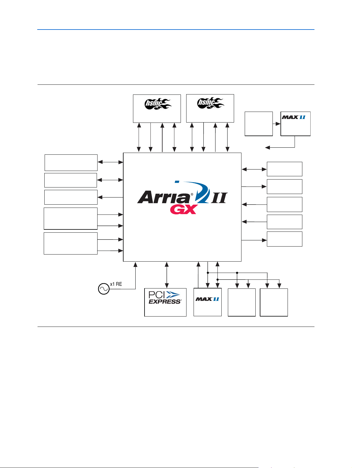
Development Board Block Diagram
Development Board Block Diagram
Figure 1–1 shows the block diagram of the Arria II GX FPGA development board, 6G
Edition.
Figure 1–1. Arria II GX FPGA Development Board, 6G Edition Block Diagram
Handling the Board
Arria II GX FPGA Development Board, 6G Edition Reference Manual © July 2010 Altera Corporation
When handling the board, it is important to observe the following static discharge
precaution:
c Without proper anti-static handling, the board can be damaged. Therefore, use
anti-static handling precautions when touching the board.
Page 9

Introduction
1 A complete set of schematics, a physical layout database, and GERBER files for the
f For information about powering up the board and installing the demonstration
2. Board Components
This chapter introduces the major components on the Arria II GX FPGA development
board, 6G Edition.
provides a brief description of all component features of the board.
development board reside in the Arria II GX development kit documents directory.
software, refer to the Arria II GX FPGA Development Kit, 6G Edition User Guide.
This chapter consists of the following sections:
■ “Board Overview”
■ “Featured Device: Arria II GX Device” on page 2–4
Figure 2–1 illustrates major component locations and Tabl e 2–1
■ “MAX II CPLD EPM2210 System Controller” on page 2–6
■ “Configuration, Status, and Setup Elements” on page 2–11
■ “Clock Circuitry” on page 2–20
■ “General User Input/Output” on page 2–23
■ “Components and Interfaces” on page 2–27
■ “Memory” on page 2–38
■ “Power Supply” on page 2–49
■ “Statement of China-RoHS Compliance” on page 2–52
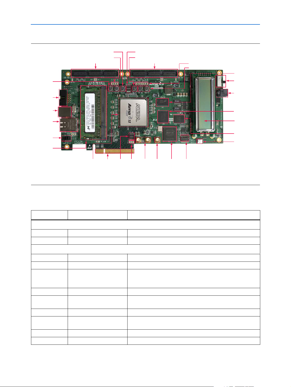
Board Overview
This section provides an overview of the Arria II GX FPGA development board, 6G
Edition, including an annotated board image and component descriptions.
provides an overview of the development board features.
Figure 2–1
© July 2010 Altera Corporation Arria II GX FPGA Development Board, 6G Edition Reference Manual
Page 10
2–2 Chapter 2: Board Components
Clock Input
SMA
Connector
(J10, J11)
Max II Reset Push-Button Switch (PB4)
General User
Push-buttons
Switches
(PB1, PB2)
Flash x16
Memory (U23)
Board
Settings
DIP Switch
(SW4)
PCI
Express
Edge
Connector
(J14)
DDR3 x16 (U13)
DC Input Jack (J4)
Arria II GX
FPGA
(U19)
Character LCD (J3)
CPU Reset Push-button Switch (PB3)
Power Switch (SW1)
User DIP Switch (SW2)
User LEDs (D7-D10)
MAX II
CPLD
EPM2210
System
Controller
(U32)
Clock
Output
SMA
Connector
(J12)
HSMC Port B (J1)
HSMC Port A (J2)
Configuration LEDs (D11-D16)
Load Image (PB5), Image Select Push-button Switch (PB6)
DDR2 SODIMM
(J7)
JTAG Connector
(J5)
USB Type-B
Connector (J6)
Gigabit Ethernet
Port (J8)
JTAG Chain
Header (J9)
Fan Power (J13)
SSRAM x36
Memory (U22)
PCI
Express
Mode
Set
(SW3)
PCI
Express
Mode
Status
(D24-D26)
Board Overview
Figure 2–1. Overview of the Arria II GX FPGA Development Board, 6G Edition Features
Tab le 2–1 describes the components and lists their corresponding board references.
Table 2–1. Arria II GX FPGA Development Board, 6G Edition Components (Part 1 of 3)
Board Reference Type Description
Featured Devices
U19 FPGA EP2AGX260FF35, 1152-pin FBGA.
U32 CPLD EPM2210F256, 256-pin FBGA.
Configuration, Status, and Setup Elements
J6 USB type-B connector Connects to the computer to enable embedded USB-Blaster JTAG.
J9 JTAG chain header Enables and disables devices in the JTAG chain.
SW4 Board settings DIP switch Controls the MAX
J5 JTAG connector Disables embedded blaster (for use with external USB-Blasters).
SW3 PCI Express DIP switch Controls the PCI Express lane width by connecting prsnt pins
as clock enable, SMA clock input control, and which image to load
from flash memory at power-up.
II CPLD EPM2210 System Controller functions such
together on the PCI Express edge connector.
D14 Configuration done LED Illuminates when the FPGA is configured.
D15 Load LED Illuminates when the MAX II CPLD EPM2210 System Controller is
actively configuring the FPGA.
D16 Error LED Illuminates when the FPGA configuration from flash memory fails.
D18 Power LED Illuminates when 2.5-V power is present.
Arria II GX FPGA Development Board, 6G Edition Reference Manual © July 2010 Altera Corporation
Page 11
Chapter 2: Board Components 2–3
Board Overview
Table 2–1. Arria II GX FPGA Development Board, 6G Edition Components (Part 2 of 3)
Board Reference Type Description
D11, D12, D13 Configuration LEDs Illuminates to show the LED sequence that determines which flash
memory image loads to the FPGA when LOAD IMAGE is pressed.
D19, D20, D21,
Ethernet LEDs Shows the connection speed as well as transmit or receive activity.
D22, D23
D4, D5 HSMC port A LEDs You can configure these LEDs to indicate transmit or receive activity.
D6 HSMC port A present LED Illuminates when a daughtercard is plugged into the HSMC port A.
D2, D3 HSMC port B LEDs You can configure these LEDs to indicate transmit or receive activity
(only populated when a EP2AGX260 device is installed).
D1 HSMC port B present LED Illuminates when a daughtercard is plugged into the HSMC port B
(only populated when a EP2AGX260 device is installed).
D24, D25, D26 PCI Express link LEDs You can configure these LEDs to display the PCI Express link width
(x1, x4, x8).
Clock Circuitry
U26 Programmable oscillator
(125 MHz default)
Programmable oscillator with a default frequency of 125.00 MHz. The
frequency is programmable using the MAX II CPLD EPM2210 System
Controller. For general use such as memories, gigabit Ethernet
(125 M/156.25 M), Serial RapidIO™ (SRIO) (125 M), or PCI Express
(100 M).
U30 Programmable oscillator
(100 MHz default)
Programmable oscillator with a default frequency of 100.00 MHz. The
frequency is programmable using the MAX II CPLD EPM2210 System
Controller. For general use such as memories, gigabit Ethernet
(125 M/156.25 M), SRIO (125 M), PCI Express (100 M), or XAUI
(156.25 M). Multiplex with CLKIN_SMA_P based on CLK_SEL
switch value.
Y5 50 MHz oscillator 50.000 MHz crystal oscillator for general purpose logic.
Y6 100 MHz oscillator 100.000 MHz crystal oscillator for general purpose logic.
U25 155.52 MHz oscillator 155.520 MHz crystal oscillator for SONET.
J10, J11 Clock input SMAs Drive LVPECL-compatible clock inputs into the clock multiplexer buffer
(U33).
J12 Clock output SMA Drive out 2.5-V CMOS clock output from the FPGA.
General User Input/Output
D7, D8, D9, D10 User LEDs Four user LEDs. Illuminates when driven low.
SW2 User DIP switch Quad user DIP switches. When the switch is ON, a logic 0 is selected.
PB3 CPU reset push-button switch Press to reset the FPGA logic.
PB4 MAX II reset push-button
Press to reset the MAX II CPLD EPM2210 System Controller.
switch
PB1, PB2 General user push-button
Two user push-button switches. Driven low when pressed.
switches
PB6 Image select push-button
switch
PB5 Load image push-button
switch
© July 2010 Altera Corporation Arria II GX FPGA Development Board, 6G Edition Reference Manual
Toggles the configuration LEDs which selects the program image that
loads from flash memory to the FPGA.
Load image from flash memory to the FGPA based on the
configuration LED setting.
Page 12
2–4 Chapter 2: Board Components
Featured Device: Arria II GX Device
Table 2–1. Arria II GX FPGA Development Board, 6G Edition Components (Part 3 of 3)
Board Reference Type Description
Memory Devices
J7 DDR2 SODIMM DDR2 x64 SODIMM 200-pin connector and is populated with a
1-Gbyte memory module.
U13 DDR3 x16 memory Independent 16-bit 128-Mbyte DDR3 memory port.
U22 SSRAM x36 memory Standard synchronous RAM which makes a 36-bit 2-Mbyte SRAM
port.
U23 Flash x16 memory Synchronous burst mode flash device which provides a 16-bit
64-Mbyte non-volatile memory port.
Communication Ports
J14 PCI Express edge connector Made of gold-plated edge fingers for up to ×8 signaling in Gen1 mode.
J2 HSMC port A Provides four transceiver channels and 80 CMOS or 17 LVDS channels
per the HSMC specification.
J1 HSMC port B Provides four transceiver channels and 78 CMOS channels per the
HSMC specification (only populated when a EP2AGX260 device is
installed).
J6 USB type-B connector USB interface for programming the FPGA through embedded
USB-Blaster JTAG via a type-B USB cable.
J8 Gigabit Ethernet RJ-45 connector which provides a 10/100/1000 Ethernet connection
via a Marvell 88E1111 PHY and the FPGA-based Altera Triple Speed
Ethernet MegaCore function in RGMII mode.
Display Ports
J3 Character LCD Connector which interfaces to the provided 16 character × 2 line LCD
module along with two standoffs at MTH7 and MTH8.
Power Supply
J14 PCI Express edge connector Interfaces to a PCI Express root port such as an appropriate PC
motherboard.
J4 DC input jack Accepts a 14-V – 20-V DC power supply. This input jack is not to be
used while the board is plugged into a PCI Express slot.
SW1 Power switch Switch to power on or off the board when power is supplied from the
DC input jack.
Featured Device: Arria II GX Device
The Arria II GX FPGA development board, 6G Edition features the Arria II GX
EP2AGX260FF35 device (U19) in a 1152-pin FBGA package.
f For more information about Arria II device family, refer to the Arria II GX Device
Handbook.
Arria II GX FPGA Development Board, 6G Edition Reference Manual © July 2010 Altera Corporation
Page 13
Chapter 2: Board Components 2–5
Featured Device: Arria II GX Device
Tab le 2–2 describes the features of the Arria II GX EP2AGX260FF35 device.
Table 2–2. Arria II GX Device EP2AGX260FF35 Features
ALMs
Equivalent
LEs
M9K RAM
Blocks
Total RAM
Kbits
18-bit × 18-bit
Multipliers PLLs Transceivers Package Type
102,600 244,188 950 11,756 736 6 16 1152-pin FBGA
Tab le 2–3 lists the Arria II GX component reference and manufacturing information.
Table 2–3. Arria II GX Device Component Reference and Manufacturing Information
Board Reference Description Manufacturer
U19 FPGA, Arria II GX F1152,
Corporation EP2AGX260FF35I3N www.altera.com
Altera
Manufacturing
Part Number
Manufacturer
Website
260K LEs, leadfree
I/O Resources
Figure 2–2 illustrates the bank organization and I/O count for the EP2AGX125 and
EP2AGX260 device in the 1152-pin FBGA package.
Figure 2–2. EP2AGX125 and EP2AGX260 Device I/O Bank Diagram
Bank 8C
Bank 8B
Bank 8A
Bank 7A
Bank 7B
GXB3
GXB2
GXB1
GXB0
Bank 3C
These I/O Banks Support:
3.3-V LVTTL/LVCMOS, 3.0-V LVTTL/LVCMOS,
2.5-V LVTTL/LVCMOS, 1.8-V LVTTL/LVCMOS,
1.5-V LVCMOS, 1.2-V LVCMOS,
Dedicated LVDS, Pseudo LVDS, RSDS, mini-LVDS,
SSTL-2, SSTL-18, SSTL-15,
HSTL-18, HSTL-15, HSTL-12,
Defferential SSTL-2, Defferential SSTL-18,
Defferential SSTL-15, Defferential HSTL-18,
Defferential HSTL-15, and Defferential HSTL-12
Bank 3B
Bank 3A
Bank 4A
Bank 6B
Bank 6A
Bank 5A
Bank 5B
Bank 4B
© July 2010 Altera Corporation Arria II GX FPGA Development Board, 6G Edition Reference Manual
Page 14
2–6 Chapter 2: Board Components
MAX II CPLD EPM2210 System Controller
Tab le 2–4 lists the I/O count for the EP2AGX125 and EP2AGX260 device.
Table 2–4. I/O Count for the EP2AGX125 and EP2AGX260 Device
Bank
Package Device
1152-pin Flip Chip
FBGA
Note to Table 2–4:
(1) Transceiver signals are not included.
EP2AGX12570—741666—66—701674— 452
EP2AGX260 70 32 74 32 66 32 66 32 70 32 74 32 612
Tab le 2–5 lists the Arria II GX device pin count and usage by function on the
development board.
Table 2–5. Arria II GX Device Pin Count and Usage
Function I/O Standard I/O Count Special Pins
DDR3 ×16 Port 1.5-V SSTL 49 2 Diff ×8 DQS
DDR2 SODIMM ×64 Port 1.8-V SSTL 120 8 Diff ×8 DQS
MAX Bus 1.5-V CMOS 8 —
Flash, SRAM, FSM Bus 2.5-V CMOS 82 —
PCI Express ×8 2.5-V CMOS + XCVR 41 1 REFCLK, 8 XCVR
HSMC Port A 2.5-V CMOS + LVDS + XCVR 104 4 XCVR, 17 LVDS, 5 Clock Inputs
HSMC Port B (1) 2.5-V CMOS + XCVR 102 4 XCVR, 1 Clock Input
Gigabit Ethernet 2.5-V CMOS + LVDS 16 1 Clock Input
Buttons 1.8-V + 2.5-V CMOS 3 1 DEV_CLRn
Switches 2.5-V CMOS 4 —
LCD 2.5-V CMOS 11 —
LEDs 2.5-V CMOS 7/9 (1) —
Clocks or Oscillators 2.5-V CMOS + LVDS + LVPECL 13/15 (1) 5 REFCLK
Tot al (1)3A 3B 4A 4B 5A 5B 6A 6B 7A 7B 8A 8B
Device I/O Total:
Note to Table 2–5:
(1) The HSMC port B is populated when the board uses an EP2AGX260 device. To support the HSMC port B, there are two additional LEDs and a
REFCLK in quadrant 3.
458/564 (1)
MAX II CPLD EPM2210 System Controller
The board utilizes the EPM2210 System Controller, an Altera MAX II CPLD, for the
following purposes:
■ FPGA configuration from flash memory
■ Power consumption monitoring
■ Virtual JTAG interface for PC-based GUI
■ Control registers for clocks
■ Control registers for remote system update
Arria II GX FPGA Development Board, 6G Edition Reference Manual © July 2010 Altera Corporation
Page 15
Chapter 2: Board Components 2–7
Information
Register
Embedded
Blaster
MAX-II
Power
Calculations
SLD-HUB
PFL
Power
Measurement
Results
Virtual-JTAG
PC
A2GX
LTC2418
Controller
FLASH
Decoder
Encoder
GPIO
JTAG Control
SSRAM
Control
Register
MAX II CPLD EPM2210 System Controller
Figure 2–3 illustrates the MAX II CPLD EPM2210 System Controller's functionality
and external circuit connections as a block diagram.
Figure 2–3. MAX II CPLD EPM2210 System Controller Block Diagram
Tab le 2–6 lists the I/O signals present on the MAX II CPLD EPM2210 System
Controller. The signal names and functions are relative to the MAX II device (U32).
Table 2–6. MAX II CPLD EPM2210 System Controller Device Pin-Out (Part 1 of 5)
Schematic Signal Name I/O Standard
EPM2210
Pin Number
EP2AGX125
Pin Number Description
clk_enable 2.5-V K14 — DIP - clock oscillator enable
clk_sel 2.5-V P2 — DIP - clock select SMA or oscillator
clk1_ce 2.5-V N3 — Programmable oscillator 1 chip select
clk1_od[0] 2.5-V M2 — Programmable oscillator 1 output divider 0
clk1_od[1] 2.5-V M1 — Programmable oscillator 1 output divider 1
clk1_od[2] 2.5-V L3 — Programmable oscillator 1 output divider 2
clk1_os[0] 2.5-V N1 — Programmable oscillator 1 output select 0
clk1_os[1] 2.5-V N2 — Programmable oscillator 1 output select 1
clk1_pr[0] 2.5-V L2 — Programmable oscillator 1 prescaler 0
clk1_pr[1] 2.5-V L1 — Programmable oscillator 1 prescaler 1
clk1_rstn 2.5-V M3 — Programmable oscillator 1 reset
clk100_cpld 2.5-V H12 — 100 MHz clock input
clk155_oe 2.5-V E1 — 155.52 MHz oscillator enable
clk2_ce 2.5-V M14 — Programmable oscillator 2 chip select
clk2_od[0] 2.5-V N16 — Programmable oscillator 2 output divider 0
clk2_od[1] 2.5-V N14 — Programmable oscillator 2 output divider 1
clk2_od[2] 2.5-V N13 — Programmable oscillator 2 output divider 2
© July 2010 Altera Corporation Arria II GX FPGA Development Board, 6G Edition Reference Manual
Page 16

2–8 Chapter 2: Board Components
MAX II CPLD EPM2210 System Controller
Table 2–6. MAX II CPLD EPM2210 System Controller Device Pin-Out (Part 2 of 5)
Schematic Signal Name I/O Standard
EPM2210
Pin Number
EP2AGX125
Pin Number Description
clk2_os[0] 2.5-V M15 — Programmable oscillator 2 output select 0
clk2_os[1] 2.5-V M16 — Programmable oscillator 2 output select 1
clk2_pr[0] 2.5-V P15 — Programmable oscillator 2 prescaler 0
clk2_pr[1] 2.5-V P14 — Programmable oscillator 2 prescaler 1
clk2_rstn 2.5-V N15 — Programmable oscillator 2 reset
csense_adc_f0 2.5-V G16 — Power monitor frequency
csense_csn[0] 2.5-V J14 — Power monitor 0 chip select
csense_csn[1] 2.5-V H15 — Power monitor 1 chip select
csense_sck 2.5-V H16 — Power monitor serial peripheral interface (SPI)
clock
csense_sdi 2.5-V H14 — Power monitor SPI data in
csense_sdo 2.5-V H13 — Power monitor SPI data out
ddr2_scl 2.5-V M7 — DDR2 SODIMM EEPROM clock
ddr2_sda 2.5-V M6 — DDR2 SODIMM EEPROM data
ep_clk 2.5-V J15 — EEPROM clock
ep_cs 2.5-V J16 — EEPROM chip select
ep_di 2.5-V K15 — EEPROM data in
ep_do 2.5-V K16 — EEPROM data out
factory_user 2.5-V L13 — Load factory or user design at power-up
flash_advn 2.5-V C8 T4 FSM bus flash memory address valid
flash_cen 2.5-V F15 M3 FSM bus flash memory chip enable
flash_clk 2.5-V C9 N4 FSM bus flash memory clock
flash_oen 2.5-V E7 K5 FSM bus flash memory output enable
flash_rdy_bsyn 2.5-V D8 R3 FSM bus flash memory ready
flash_resetn 2.5-V D15 N3 FSM bus flash memory reset
flash_wen 2.5-V D7 C7 FSM bus flash memory write enable
fpga_conf_done 2.5-V J1 AE25 FPGA configuration done
fpga_config_d[0] 2.5-V B1 N26 FPGA configuration data
fpga_config_d[1] 2.5-V A4 N6 FPGA configuration data
fpga_config_d[2] 2.5-V A7 G2 FPGA configuration data
fpga_config_d[3] 2.5-V B4 P6 FPGA configuration data
fpga_config_d[4] 2.5-V B5 L4 FPGA configuration data
fpga_config_d[5] 2.5-V A6 K3 FPGA configuration data
fpga_config_d[6] 2.5-V A5 M4 FPGA configuration data
fpga_config_d[7] 2.5-V B6 K2 FPGA configuration data
fpga_dclk 2.5-V H4 L25 FPGA configuration clock
fpga_nconfig 2.5-V J2 AC26 FPGA configuration active
fpga_nstatus 2.5-V H3 AD28 FPGA configuration ready
fsm_a[0] 2.5-V A2 M21 FSM bus address
Arria II GX FPGA Development Board, 6G Edition Reference Manual © July 2010 Altera Corporation
Page 17
Chapter 2: Board Components 2–9
MAX II CPLD EPM2210 System Controller
Table 2–6. MAX II CPLD EPM2210 System Controller Device Pin-Out (Part 3 of 5)
Schematic Signal Name I/O Standard
EPM2210
Pin Number
EP2AGX125
Pin Number Description
fsm_a[1] 2.5-V D9 J3 FSM bus address
fsm_a[10] 2.5-V B16 C24 FSM bus address
fsm_a[11] 2.5-V C15 E25 FSM bus address
fsm_a[12] 2.5-V D16 F21 FSM bus address
fsm_a[13] 2.5-V D10 J19 FSM bus address
fsm_a[14] 2.5-V A15 H19 FSM bus address
fsm_a[15] 2.5-V C11 K21 FSM bus address
fsm_a[16] 2.5-V A12 L21 FSM bus address
fsm_a[17] 2.5-V B12 F25 FSM bus address
fsm_a[18] 2.5-V C12 F26 FSM bus address
fsm_a[19] 2.5-V B13 G23 FSM bus address
fsm_a[2] 2.5-V E10 D29 FSM bus address
fsm_a[20] 2.5-V A13 H21 FSM bus address
fsm_a[21] 2.5-V B14 M13 FSM bus address
fsm_a[22] 2.5-V D11 P7 FSM bus address
fsm_a[23] 2.5-V E9 F10 FSM bus address
fsm_a[24] 2.5-V D6 R4 FSM bus address
fsm_a[25] 2.5-V C13 K4 FSM bus address
fsm_a[3] 2.5-V E4 J21 FSM bus address
fsm_a[4] 2.5-V E5 L13 FSM bus address
fsm_a[5] 2.5-V E14 C8 FSM bus address
fsm_a[6] 2.5-V G15 N9 FSM bus address
fsm_a[7] 2.5-V E15 D20 FSM bus address
fsm_a[8] 2.5-V F16 A23 FSM bus address
fsm_a[9] 2.5-V E16 B24 FSM bus address
fsm_d[0] 2.5-V E11 A19 FSM bus data
fsm_d[1] 2.5-V E12 C18 FSM bus data
fsm_d[10] 2.5-V E13 D24 FSM bus data
fsm_d[11] 2.5-V D13 A25 FSM bus data
fsm_d[12] 2.5-V C5 B25 FSM bus data
fsm_d[13] 2.5-V C4 A26 FSM bus data
fsm_d[14] 2.5-V C7 C26 FSM bus data
fsm_d[15] 2.5-V C10 A27 FSM bus data
fsm_d[16] 2.5-V C2 R9 FSM bus data
fsm_d[17] 2.5-V D3 R10 FSM bus data
fsm_d[18] 2.5-V E3 R8 FSM bus data
fsm_d[19] 2.5-V D2 A17 FSM bus data
fsm_d[2] 2.5-V D12 D28 FSM bus data
fsm_d[20] 2.5-V E2 D22 FSM bus data
© July 2010 Altera Corporation Arria II GX FPGA Development Board, 6G Edition Reference Manual
Page 18
2–10 Chapter 2: Board Components
MAX II CPLD EPM2210 System Controller
Table 2–6. MAX II CPLD EPM2210 System Controller Device Pin-Out (Part 4 of 5)
Schematic Signal Name I/O Standard
EPM2210
Pin Number
EP2AGX125
Pin Number Description
fsm_d[21] 2.5-V D1 T10 FSM bus data
fsm_d[22] 2.5-V F1 P4 FSM bus data
fsm_d[23] 2.5-V F3 R11 FSM bus data
fsm_d[24] 2.5-V G2 A18 FSM bus data
fsm_d[25] 2.5-V F2 B18 FSM bus data
fsm_d[26] 2.5-V G3 C19 FSM bus data
fsm_d[27] 2.5-V G1 D19 FSM bus data
fsm_d[28] 2.5-V H1 B21 FSM bus data
fsm_d[29] 2.5-V G4 A21 FSM bus data
fsm_d[3] 2.5-V C14 B19 FSM bus data
fsm_d[30] 2.5-V J4 C21 FSM bus data
fsm_d[31] 2.5-V H2 A22 FSM bus data
fsm_d[4] 2.5-V E8 E19 FSM bus data
fsm_d[5] 2.5-V D4 E18 FSM bus data
fsm_d[6] 2.5-V C6 G19 FSM bus data
fsm_d[7] 2.5-V D5 F19 FSM bus data
fsm_d[8] 2.5-V E6 D21 FSM bus data
fsm_d[9] 2.5-V D14 D23 FSM bus data
hsma_psnt_n 2.5-V A10 U3 HSMC port A present
hsmb_psnt_n 2.5-V J13 AG28 HSMC port B present
led_config_led[0] 2.5-V B8 — Flash memory image select indicator
led_config_led[1] 2.5-V A8 — Flash memory image select indicator
led_config_led[2] 2.5-V B7 — Flash memory image select indicator
factory
(IMAGE SEL)
2.5-V B9 — Toggles the LED_CONFIG_LED[2:0]
sequence.
lcd_pwrmon 2.5-V K13 — DIP - MAX II LCD drive enable
reset_confign
(LOAD IMAGE)
2.5-V A9 — Load the flash memory identified by the
configuration LEDs
max_dip[0] 2.5-V L16 — DIP - reserved
max_dip[1] 2.5-V L15 — DIP - reserved
max_dip[2] 2.5-V L14 — DIP - reserved
max_error 2.5-V B10 — FPGA configuration error LED
max_led 2.5-V B11 — LED - reserved
max_load 2.5-V A11 — FPGA configuration active LED
max_resetn 2.5-V M9 — MAX II reset push-button
max2_ben[0] 2.5-V M11 C15 FSM bus Max2 byte enable 0
max2_ben[1] 2.5-V M10 H16 FSM bus Max2 byte enable 1
max2_ben[2] 2.5-V N12 D14 FSM bus Max2 byte enable 2
max2_ben[3] 2.5-V P12 A9 FSM bus Max2 byte enable 3
Arria II GX FPGA Development Board, 6G Edition Reference Manual © July 2010 Altera Corporation
Page 19
Chapter 2: Board Components 2–11
Configuration, Status, and Setup Elements
Table 2–6. MAX II CPLD EPM2210 System Controller Device Pin-Out (Part 5 of 5)
EPM2210
Schematic Signal Name I/O Standard
max2_clk 2.5-V N10 J14 FSM bus Max2 clock
max2_csn 2.5-V M12 A16 FSM bus Max2 chip select
max2_oen 2.5-V M8 A14 FSM bus Max2 output enable
max2_wen 2.5-V N11 B16 FSM bus Max2 write enable
sram_mode 2.5-V J3 — FSM bus SSRAM burst sequence selection
sram_zz 2.5-V B3 B27 FSM bus SSRAM power sleep mode
usb_disablen 2.5-V K2 — DIP - embedded USB-Blaster disable
usb_led 2.5-V K1 — Embedded USB-Blaster active
Pin Number
EP2AGX125
Pin Number Description
Tab le 2–7 lists the MAX II CPLD EPM2210 System Controller component reference
and manufacturing information.
Table 2–7. MAX II CPLD EPM2210 System Controller Component Reference and Manufacturing Information
Board Reference Description Manufacturer
U32 IC - MAX II CPLD EPM2210
256FBGA -3 LF 2.5V VCCINT
Corporation EPM2210F256C3N www.altera.com
Altera
Manufacturing
Part Number
Manufacturer
Configuration, Status, and Setup Elements
Website
Configuration
This section describes the board's configuration, status, and setup elements.
This section describes the FPGA, flash memory, and MAX II CPLD EPM2210 System
Controller device programming methods supported by the Arria II GX FPGA
development board, 6G Edition. The Arria II GX FPGA development board, 6G
Edition supports the following three configuration methods:
■ Embedded USB-Blaster is the default method for configuring the FPGA at any
time using the Quartus II Programmer in JTAG mode with the supplied USB cable.
■ External USB-Blaster for configuring the FPGA using the external USB-Blaster.
■ Flash memory download is used for configuring the FPGA using stored images
from the flash memory on either power-up or pressing the LOAD IMAGE
push-button switch (PB5).
FPGA Programming over Embedded USB-Blaster
The USB-Blaster is implemented using a USB Type-B connector (J6), a FTDI USB 2.0
PHY device (U15), and an Altera MAX II CPLD (U32). This allows the configuration
of the FPGA using a USB cable directly connected between the USB port on the board
(J6) and a USB port of a PC running the Quartus II software. The JTAG chain is
normally mastered by the embedded USB-Blaster found in the MAX
EPM240Z.
II CPLD
© July 2010 Altera Corporation Arria II GX FPGA Development Board, 6G Edition Reference Manual
Page 20

2–12 Chapter 2: Board Components
Embedded
Blaster
GPIO
TCK
EP2AGX125
FPGA
Analog
Switch
MAX II CPLD
EPM2210
System
Controller
HSMC
Port A
HSMC
Port B
GPIO
TMS
GPIO
TDO
GPIO
TDI
JTAG Master
GPIO
DISABLE
JTAG Master/Slave
JTAG Master/Slave
Installed
HSMC
Card
Installed
HSMC
Card
TCK
TMS
TDI
TDO
TCK
TMS
TDI
TDO
TCK
TMS
TDI
TDO
TCK
TMS
TDI
TDO
JTAG Slave
JTAG Slave
Analog
Switch
Analog
Switch
MAX_JTAG_EN
HSMA_JTAG_EN
HSMB_JTAG_EN
ALWAYS
ENABLED
(in chain)
SW4.6
10-pin
JTAG Connector
Flash
Memory
(on install)
PCI Express
Edge
Connector
JTAG Master/Slave
PCI Express
Motherboard
TCK
TMS
TDI
TDO
Analog
Switch
PCIE_JTAG_EN
USB Type-B
Connector
USB
PHY
J6
J5
JTAG
Chain Header
2x4 Jumper
J9
Configuration, Status, and Setup Elements
The embedded USB-Blaster is automatically disabled when an external USB-Blaster is
connected to the JTAG chain.
Figure 2–4 illustrates the JTAG chain.
Figure 2–4. JTAG Chain
Each jumper shown in Figure 2–4 is located in the JTAG chain header (J9) on the front
of the board. To connect a device or interface in the chain, the corresponding shunt
must be removed from the jumper. Install a shunt on each of the four jumper positions
to only have the FPGA in the chain.
The MAX II CPLD EPM2210 System Controller must be in the chain to use some of the
GUI interfaces. For this setting, remove the left-most jumper shunt from the JTAG
chain header (J9).
Flash Memory Programming
Flash memory programming is possible through a variety of methods using the Arria
II GX device.
Arria II GX FPGA Development Board, 6G Edition Reference Manual © July 2010 Altera Corporation
Page 21

Chapter 2: Board Components 2–13
Configuration, Status, and Setup Elements
The default method is to use the factory design called the Board Update Portal. This
design is an embedded webserver, which serves the Board Update Portal web page.
The web page allows you to select new FPGA designs including hardware, software,
or both in an industry-standard S-Record File (.flash) and write the design to the user
hardware page (page 1) of the flash memory over the network.
The secondary method is to use the pre-built parallel flash loader (PFL) design
included in the development kit. The development board implements the Altera PFL
megafunction for flash memory programming. The PFL megafunction is a block of
logic that is programmed into an Altera programmable logic device (FPGA or CPLD).
The PFL functions as a utility for writing to a compatible flash memory device. This
pre-built design contains the PFL megafunction that allows you to write either page 0,
page 1, or other areas of flash memory over the USB interface using the Quartus II
software. This method is used to restore the development board to its factory default
settings.
Other methods to program the flash memory can be used as well, including the
®
Nios
II processor.
f For more information on the Nios II processor, refer to the Nios II Processor page of
the Altera website.
FPGA Programming from Flash Memory
On either power-up or by pressing the load image push-button switch (PB5), the
MAX
II CPLD EPM2210 System Controller's PFL configures the FPGA from the flash
memory when the CONFIG_LED0 is ON. The PFL megafunction reads 16-bit data
from the flash memory and converts it to fast passive parallel (FPP) format. This 8-bit
data is then written to the FPGA's dedicated configuration pins during configuration.
© July 2010 Altera Corporation Arria II GX FPGA Development Board, 6G Edition Reference Manual
Page 22

2–14 Chapter 2: Board Components
MAX II CPLD
EPM2210 System Controller
FPGA_DATA [7:0]
FPGA_DCLK
FLASH_A [25:1]
FLASH_D [15:0]
DATA [7:0]
DCLK
INIT_DONE
nSTATUS
nCONFIG
CONF_DONE
MSEL0
MSEL1
MSEL2
MSEL3
2.5 V
10 kΩ
nCE
CFI
Flash
10 kΩ
FLASH_CEn
FLASH_OEn
FLASH_WEn
FLASH_A [25:1]
FLASH_D [15:0]
FLASH_CEn
FLASH_OEn
FLASH_WEn
FLASH_RSTn
FLASH_ADVn
MSEL [3:0]
FPGA_nCONFIG
FPGA_CONF_DONE
FLASH_RYBSYn
FPGA_nSTATUS
2.5 V
10 kΩ
FLASH_ADVn
CONF_DONE_LED
2.5 V
FLASH_CLK
FLASH_CLK
FLASH_RSTn
FLASH_RSTn
FPP Port
Flash Interface
100 Ω
100 MHz
2.5 V
2.5 V
ERROR
MAX_LED
LOAD
DIP0
DIP1
DIP1
FACTORY/USER LOAD
LCD_PWRMON
USB_DISABLEn
CLK_EN
CLK_SEL
MAX_RESETn
LOAD_IMAGE
(RESET_CONF
IGN)
IMAGE_SEL
(FACTORY)
CONFIG_LED0
CONFIG_LED1
CONFIG_LED2
DIP Switch
Configuration, Status, and Setup Elements
Figure 2–5 shows the PFL configuration.
Figure 2–5. PFL Configuration
Arria II GX FPGA Development Board, 6G Edition Reference Manual © July 2010 Altera Corporation
Page 23

Chapter 2: Board Components 2–15
Configuration, Status, and Setup Elements
Tab le 2–8 shows the flash memory map storage.
Table 2–8. Flash Memory Map
Name Size (Kbyte) Address
Unused 32 0x03FF.FFFF
0x03FF.8000
32 0x03FF.7FFF
0x03FF.0000
32 0x03FE.FFFF
0x03FE.8000
32 0x03FE.7FFF
0x03FE.0000
User software 16,384 0x03FD.FFFF
0x0300.0000
Factory software 8,192 0x02FF.FFFF
0x0280.0000
zipfs—HTML, web content 8,192 0x027F.FFFF
0x0200.0000
User hardware 2 11,141 0x01FF.FFFF
0x0156.0000
User hardware 1 11,141 0x0155.FFFF
0x00AC.0000
Factory hardware 11,141 0x00AB.FFFF
0x0002.0000
PFL option bits 32 0x0001.FFFF
0x0001.8000
Board information 32 0x0001.7FFF
0x0001.0000
Ethernet option bits (MAC address) 32 0x0000.FFFF
0x0000.8000
User design reset vector 32 0x0000.7FFF
0x0000.0000
There are two pages reserved for the FPGA configuration data. The factory hardware
page is considered page 0 and is loaded upon power-up if the USER LOAD DIP switch
(SW4.4) is set to '1'. Otherwise, the user hardware page 1 is loaded. Pressing the load
image push-button switch (PB5) loads the FPGA with a hardware page based on
which CONFIG[2:0] LED (D11, D12, D13) is illuminated.
Tab le 2–9 defines the
hardware page that loads when the load image push-button switch (PB5) is pressed.
© July 2010 Altera Corporation Arria II GX FPGA Development Board, 6G Edition Reference Manual
Page 24

2–16 Chapter 2: Board Components
Configuration, Status, and Setup Elements
Table 2–9. Load Image Push-Button Switch (PB5) LED Settings (1) (2)
IMAGE0 IMAGE1 IMAGE2 Design
ON OFF OFF Factory hardware
OFF ON OFF User hardware 1
OFF OFF ON User hardware 2
Notes to Table 2–9:
(1) ON indicates a setting of ’1’.
(2) OFF indicates a setting of ’0’.
FPGA Programming over External USB-Blaster
The JTAG programming header provides another method for configuring the FPGA
(U19) using an external USB-Blaster device with the Quartus II Programmer running
on a PC. The external USB-Blaster is connected to the board through the JTAG
connector (J5). Install a shunt onto the JTAG chain header (J9) pins 1 and 2 to remove
the MAX II CPLD device from the JTAG chain so that the FPGA is the only device on
the JTAG chain.
f For more information on the following topics, refer to the respective documents:
■ Board Update Portal, refer to the Arria II GX FPGA Development Kit, 6G Edition User
Guide.
■ PFL design, refer to the Arria II GX FPGA Development Kit, 6G Edition User Guide.
■ PFL megafunction, refer to Parallel Flash Loader Megafunction User Guide.
Status Elements
The development board includes status LEDs. This section describes the status
elements.
Tab le 2–10 lists the LED board references, names, and functional descriptions.
Table 2–10. Board-Specific LEDs (Part 1 of 2)
Board Reference LED Name Description
D18 Power Blue LED. Illuminates when 2.5 V power is active.
D14 CONF DONE Green LED. Illuminates when the FPGA is successfully configured. Driven by the
MAX II CPLD EPM2210 System Controller.
D15 Loading Green LED. Illuminates when the MAX II CPLD EPM2210 System Controller is
actively configuring the FPGA. Driven by the MAX II CPLD EPM2210 System
Controller wire-OR'd with the embedded USB-Blaster CPLD.
D16 Error Red LED. Illuminates when the MAX II CPLD EPM2210 System Controller fails to
configure the FPGA. Driven by the MAX II CPLD EPM2210 System Controller.
D11, D12, D13 CONFIG[2:0] Green LEDs. Illuminates to indicate which hardware page loads from flash
memory.
D19 ENET TX Green LED. Illuminates to indicate Ethernet PHY transmit activity. Driven by the
Marvell 88E1111 PHY.
D20 ENET RX Green LED. Illuminates to indicate Ethernet PHY receive activity. Driven by the
Marvell 88E1111 PHY.
Arria II GX FPGA Development Board, 6G Edition Reference Manual © July 2010 Altera Corporation
Page 25

Chapter 2: Board Components 2–17
Configuration, Status, and Setup Elements
Table 2–10. Board-Specific LEDs (Part 2 of 2)
Board Reference LED Name Description
D23 10 Green LED. Illuminates to indicate Ethernet linked at 10 Mbps connection speed.
Driven by the Marvell 88E1111 PHY.
D22 100 Green LED. Illuminates to indicate Ethernet linked at 100 Mbps connection speed.
Driven by the Marvell 88E1111 PHY.
D21 1000 Green LED. Illuminates to indicate Ethernet linked at 1000 Mbps connection speed.
Driven by the Marvell 88E1111 PHY.
D6 HSMC Port A
Present
D1 HSMC Port B
Present
Green LED. Illuminates when HSMC port A has a board or cable plugged-in such
that pin 160 becomes grounded. Driven by the add-in card.
Green LED. Illuminates when HSMC port B has a board or cable plugged-in such
that pin 160 becomes grounded. Driven by the add-in card.
D24 PCIe x1 Green LED. Configure this LED to display the PCI Express link width x1.
D25 PCIe x4 Green LED. Configure this LED to display the PCI Express link width x4.
D26 PCIe x8 Green LED. Configure this LED to display the PCI Express link width x8.
Tab le 2–11 lists the board-specific LEDs component references and manufacturing
information.
Table 2–11. Board-Specific LEDs Component References and Manufacturing Information
Manufacturer
Board Reference Description Manufacturer
D1, D6, D11-D16,
Green LEDs Lite-On LTST-C170KGKT www.us.liteon.com/opto.index.html
Part Number Manufacturer Website
D19-D26
D16 Red LED Lite-On LTST-C170KRKT www.us.liteon.com/opto.index.html
D18 Blue LED Lite-On LTST-C170TBKT www.us.liteon.com/opto.index.html
Setup Elements
The development board includes several different kinds of setup elements. This
section describes the following setup elements:
■ Board settings DIP switch
■ JTAG chain header switch
■ PCI Express control DIP switch
■ Reset configuration push-button switches
Board Settings DIP Switch
The board settings DIP switch (SW4) controls various features specific to the board
and the MAX
switch controls and descriptions.
II CPLD EPM2210 System Controller logic design. Tab le 2–12 shows the
Table 2–12. Board Settings DIP Switch Controls (Part 1 of 2)
Switch Schematic Signal Name Description Default
1 MAX_DIP0 Reserved OFF
2 MAX_DIP1 Reserved OFF
© July 2010 Altera Corporation Arria II GX FPGA Development Board, 6G Edition Reference Manual
Page 26

2–18 Chapter 2: Board Components
Configuration, Status, and Setup Elements
Table 2–12. Board Settings DIP Switch Controls (Part 2 of 2)
Switch Schematic Signal Name Description Default
3 MAX_DIP2 Reserved OFF
4 MAX_DIP3 ON : Load User hardware page 1 from flash memory upon power-up
OFF
OFF : Load factory design from flash memory upon power-up
5 LCD_PWRMON ON : LCD driven from the MAX II EPM2210 System Controller (power
ON
monitor)
OFF : Unused
6 USB_DISABLEn ON : Embedded USB-Blaster disable
OFF
OFF : Embedded USB-Blaster enable
7 CLK_ENABLE ON : On-board oscillators enable
ON
OFF : On-board oscillators disable
8 CLK_SEL ON : 100 MHz clock select
ON
OFF : SMA input clock select
Tab le 2–13 lists the board settings DIP switch component reference and
manufacturing information.
Table 2–13. Board Settings DIP Switch Component Reference and Manufacturing Information
Manufacturer
Board Reference Description Manufacturer
Part Number Manufacturer Website
SW4 Eight-position slide DIP switch HCH HPS608-E www.hchtwn.com.tw
JTAG Chain Header Switch
The JTAG chain header switch (J9) is provided to either remove or include devices in
the active JTAG chain. However, the Arria II GX FPGA device is always in the JTAG
chain.
Tab le 2–14 shows the switch controls and its descriptions.
Table 2–14. JTAG Chain Header Switch Controls
Switch Schematic Signal Name Description Default
1 MAX_JTAG_EN ON : Bypass MAX II CPLD EPM2210 System Controller
OFF : MAX II CPLD EPM2210 System Controller in-chain
2 HSMA_JTAG_EN ON : Bypass HSMA
OFF : HSMA in-chain
3 HSMB_JTAG_EN ON : Bypass HSMB
OFF : HSMB in-chain
4 PCIE_JTAG_EN ON : Bypass PCI Express
OFF : Reserved (disables JTAG chain, do not use)
ON
ON
ON
ON
Arria II GX FPGA Development Board, 6G Edition Reference Manual © July 2010 Altera Corporation
Page 27

Chapter 2: Board Components 2–19
Configuration, Status, and Setup Elements
Tab le 2–15 lists the JTAG chain header switch component reference and
manufacturing information.
Table 2–15. JTAG Chain Header Switch Component Reference and Manufacturing Information
Manufacturer
Board Reference Device Description Manufacturer
J9 2x4 100 mil jumper Leamax Enterprise Co. 21312*4SE www.leamax.com
Part Number Manufacturer Website
PCI Express Control DIP Switch
The PCI Express control DIP switch (SW3) is provided to enable or disable different
configurations.
Table 2–16. PCI Express Control DIP Switch Controls
Switch Schematic Signal Name Description Default
1 PCIE_PRSNT2n_x1 ON : Enable x1 presence detect
2 PCIE_PRSNT2n_x4 ON : Enable x4 presence detect
3 PCIE_PRSNT2n_x8 ON : Enable x8 presence detect
4 NC Not used OFF
Ta bl e 2–16 shows the switch controls and descriptions.
ON
OFF : Disable x1 presence detect
ON
OFF : Disable x4 presence detect
ON
OFF : Disable x8 presence detect
Tab le 2–17 lists the PCI Express control DIP switch component reference and
manufacturing information.
Table 2–17. PCI Express Control DIP Switch Component Reference and Manufacturing Information
Manufacturer
Board Reference Description Manufacturer
SW3 Four-position slide DIP switch HCH HPS604-E www.hchtwn.com.tw
Part Number Manufacturer Website
Reset Configuration Push-button Switches
The load image push-button switch, RESET_CONFIGn (LOAD IMAGE) (PB5), is an
input to the MAX
a reconfiguration of the FPGA from flash memory. The location in the flash memory is
based on the LED_CONFIG_LED[2:0] setting when the button is released. Valid
settings include LED_CONFIG_LED0, LED_CONFIG_LED1, or LED_CONFIG_LED2 on
the three pages in flash memory reserved for FPGA designs.
The image select push-button switch, factory (IMAGE SEL)(PB6), toggles the
LED_CONFIG_LED[2:0] sequence. Refer to
LED_CONFIG_LED[2:0] sequence definitions.
The MAX II reset push-button switch, MAX_RESETn (PB4), resets the MAX II CPLD
EPM2210 System Controller.
II CPLD EPM2210 System Controller. The push-button switch forces
Tab le 2–9 for the
© July 2010 Altera Corporation Arria II GX FPGA Development Board, 6G Edition Reference Manual
Page 28

2–20 Chapter 2: Board Components
Q0Q1Q2Q3
3B 3A 4A 4B
8B 8A 7A 7B
6B 6A 5A 5B
PLL 1
PLL 2 PLL 3
PLL 4
EP2AGX260FF35
Control signals route to
MAX II CPLD EPM2210
System Controller
155.52 M
CLK_SEL
REFCLK INPUT
SMA SMA
(LVPECL)
2-to-4 buffer
MAX II CPLD
EPM2210 System Controller
25 MHz
Crystal
3.3V
Low Jitter Clock
Generator*
(Default 125 MHz)
CDCM61004RHB
XIN 2
(LVDS)
3.3V
(LVPECL)
CLK2_RSTn
CLK2_PR1
3.3V
PCIE_REFCLK_P/N
XIN 1
7 6 5 4 3 2 1 07 6 5 4 3 2 1 0
(LVDS)
HSMA_CLK_IN_P[2] / N[2]
(LVDS)
HSMB_CLK_IN0
HSMA_CLK_IN0
* CDCM6100x can be set to output frequencies
of 100 MHz, 125 MHz, 156.25 MHz.
PLL5PLL
6
25 MHz
Crystal
CLK_IN_TOP_P/N
CLK_IN_BOT_P/N
100 M50 M
ENET_RX_CLK
(2.5 V)
Low Jitter Clock
Generator*
(Default 100 MHz)
CDCM61001RHB
(2.5 V) (2.5 V)
(LVDS)
(LVDS)
(LVDS)
(LVDS)
(LVDS)
CLK2_CE
CLK2_OS1
CLK2_OS0
CLK2_PR0
CLK2_OD2
CLK2_OD1
CLK2_OD0
CLK1_RSTn
CLK1_CE
CLK1_OS1
CLK1_OS0
CLK1_PR1
CLK1_PR0
CLK1_OD2
CLK1_OD1
CLK1_OD0
HSMA_CLK_IN_P[1] / N[1]
Clock Circuitry
Tab le 2–18 lists the reset configuration push-button switches component reference
and manufacturing information.
Table 2–18. Reset Configuration Push-button Switches Component Reference and Manufacturing Information
Board
Reference Description Manufacturer
Manufacturer
Part Number Manufacturer Website
PB4, PB5, PB6 Push-button Switch Dawning Precision Co. TS-A02SA-2-S100 http://www.dawning2.com.tw/
company.php
Clock Circuitry
This section describes the board's clock inputs and outputs.
Arria II GX FPGA Clock Inputs
The development board has two types of clock inputs: global clock inputs and
transceiver reference clock inputs.
Figure 2–6 shows the Arria II GX FPGA development board, 6G Edition clock inputs.
Figure 2–6. Arria II GX FPGA Development Board, 6G Edition Clock Inputs
Arria II GX FPGA Development Board, 6G Edition Reference Manual © July 2010 Altera Corporation
Page 29

Chapter 2: Board Components 2–21
Clock Circuitry
Tab le 2–19 shows the external clock inputs for the Arria II GX FPGA development
board, 6G Edition.
Table 2–19. Arria II GX FPGA Development Board, 6G Edition Clock Inputs
Source Schematic Signal Name Pin I/O Standard Description
U25 CLK_155_P R29 LVPECL 155.52 MHz oscillator which drives the
transceiver Q2 reference clock input with
100 Ω OCT.
LVDS input to the bottom edge of PLL input.
LVDS input to the transceiver Q2 reference
clock input with 100 Ω OCT.
input to the top edge of PLL input.
SMA or
100.000 MHz
(Default
Frequency) (1)
125.000 MHz
(Default
Frequency) (2)
CLK_155_N R30
CLKIN_BOT_P AJ19 LVDS Input to the fan-out buffer (U33) which drives
CLKIN_BOT_N AK19
CLKIN_REF_Q2_P U29 Input to the fan-out buffer (U33) which drives
CLKIN_REF_Q2_N U30
CLKIN_TOP_P F18 LVDS Programmable oscillator which drives LVDS
CLKIN_TOP_N F17
CLK_REF_Q1_1_P AA29 Programmable oscillator which drives LVDS
CLK_REF_Q1_1_N AA30
CLK_REF_Q1_2_P W29
input to the transceiver Q1 reference clock
input with 100 Ω OCT.
CLK_REF_Q1_2_N W30
CLK_REF_Q3_P N29 Programmable oscillator which drives LVDS
CLK_REF_Q3_N N30
input to the transceiver Q3 reference clock
input with 100 Ω OCT.
Samtec HSMC HSMA_CLKIN0 AP17 LVTTL Single-ended input from the installed HSMC
port A cable or board.
Samtec HSMC HSMA_CLKIN_P1 U6 LVDS or LVTTL LVDS input from the installed HSMC port A
HSMA_CLKIN_N1 U5
cable or board. Can also support two LVTTL
inputs.
Samtec HSMC HSMA_CLKIN_P2 K18 LVDS or LVTTL LVDS input from the installed HSMC port A
HSMA_CLKIN_N2 J18
cable or board. Can also support two LVTTL
inputs.
Samtec HSMC HSMB_CLKIN0 AP16 LVTTL Single-ended input from the installed HSMC
port B cable or board.
PCI Express
Edge
Notes to Table 2–19:
(1) CDCM61001 has a default frequency of 100 MHz, but can also be set by the MAX II CPLD to frequencies of 125 MHz and 156.25 MHz.
(2) CDCM61004 has a default frequency of 125 MHz, but can also be set by the MAX II CPLD to frequencies of 100 MHz and 156.25 MHz.
PCIE_REFCLK_P AE29 HCSL High-Speed Current Steering Logic (HCSL)
PCIE_REFCLK_N AE30
input from the PCI Express edge connector.
© July 2010 Altera Corporation Arria II GX FPGA Development Board, 6G Edition Reference Manual
Page 30

2–22 Chapter 2: Board Components
Q0Q1Q2Q3
3B 3A 4A 4B
8B 8A 7A 7B
6B 6A 5A 5B
PLL 1
PLL 2 PLL 3
PLL 4
EP2AGX260FF35
7 6 5 4 3 2 1 07 6 5 4 3 2 1 0
HSMA_CLKOUT_P[1] / N[1]
(LVDS)
HSMB_CLKOUT_P[2] / N[2]
(LVD S)
HSMB_CLKOUT0
HSMA_CLKOUT0
PLL5PLL
6
CLOCK_SMA
SMA
DDR3_CLK_P/N
(Differential SSTL-15)
HSMA_CLKOUT_P[2] / N[2]
(LVDS)
(2.5 V)
HSMB_CLKOUT_P[2] / N[2]
(LVDS)
DDR2_CLK_P/N[1:0]
(Differential SSTL-18)
(2.5 V)
(2.5 V)
Clock Circuitry
Arria II GX FPGA Clock Outputs
Figure 2–7 shows the Arria II GX FPGA development board, 6G Edition clock
outputs.
Figure 2–7. Arria II GX FPGA Development Board, 6G Edition Clock Outputs
Table 2–20. Arria II GX FPGA Development Board, 6G Edition Clock Outputs
Connector Schematic Signal Name Pin I/O Standard Description
Samtec HSMC HSMA_CLKOUT0 P10 2.5-V FPGA CMOS output or GPIO
Samtec HSMC HSMA_CLKOUT_P1 AD7 LVDS or 2.5-V LVDS output or two 2.5-V CMOS outputs.
Samtec HSMC HSMA_CLKOUT_P2 V12 LVDS or 2.5-V LVDS output or two 2.5-V CMOS outputs.
Samtec HSMC HSMB_CLKOUT0 AG30 2.5-V FPGA CMOS output or GPIO
Arria II GX FPGA Development Board, 6G Edition Reference Manual © July 2010 Altera Corporation
Tab le 2–20 lists the clock outputs for the Arria II GX FPGA development board, 6G
Edition.
SMA CLKOUT_SMA F23 2.5-V FPGA CMOS output or general purpose I/O (GPIO)
HSMA_CLKOUT_N1 AD6
HSMA_CLKOUT_N2 W12
Page 31

Chapter 2: Board Components 2–23
General User Input/Output
Tab le 2–21 lists the crystal oscillators component references and manufacturing
information.
Table 2–21. Crystal Oscillator Component References and Manufacturing Information
Board
Reference Description Manufacturer
U25 156.25 MHz LVPECL Saw
Oscillator
U26 Quad Output Programmable
Clock Generator
U30 Single Output Programmable
Clock Generator
Y6 100 MHz Crystal Oscillator Mercury Electronics 3H53-AT-100.000 www.mecxtal.com
Y5 50 MHz Crystal Oscillator Epson XG-1000CB
Epson EG-2102CA
Texas Instruments CDCM61004RHBR www.ti.com
Texas Instruments CDCM61001RHBR www.ti.com
Manufacturer
Part Number Manufacturer Website
www.eea.epson.com
155.5200M-DGPA
www.eea.epson.com
50.0000M-DCL3
General User Input/Output
This section describes the user I/O interface to the FPGA, including the push-buttons,
DIP switches, status LEDs, and character LCD.
User-Defined Push-Button Switches
The development board includes three user-defined push-button switches: two
general user push-button switches and one CPU reset. For information on the system
and safe reset push-button switches, refer to
Switches” on page 2–19.
“Reset Configuration Push-button
Board references PB1 and PB2 are push-button switches that allow you to interact
with the Arria II GX device. When the switch is pressed and held down, the device
pin is set to logic 0; when the switch is released, the device pin is set to logic 1. There is
no board-specific function for these general user push-button switches.
The board reference PB3 is the CPU reset push-button switch, CPU_RESET, which is
an input to the Arria II GX device. CPU_RESET is intended to be the master reset
signal for the FPGA design loaded into the Arria II GX device. It also acts as a regular
I/O pin.
Tab le 2–22 lists the user-defined push-button switch schematic signal names and their
corresponding Arria II GX device pin numbers.
Table 2–22. User-defined Push-button Switch Schematic Signal Names and Functions
Schematic Signal
Board Reference Description
PB2
PB1 USER_PB1 AL7
PB3 CPU_RESET 2.5-V N10
User-defined push-button switch
Name I/O Standard
USER_PB0
1.8-V
Arria II GX Device
Pin Number
AK9
© July 2010 Altera Corporation Arria II GX FPGA Development Board, 6G Edition Reference Manual
Page 32

2–24 Chapter 2: Board Components
General User Input/Output
Tab le 2–23 lists the user-defined push-button switch component reference and the
manufacturing information.
Table 2–23. User-defined Push-button Switch Component Reference and Manufacturing Information
Manufacturer
Board Reference Description Manufacturer
PB1 to PB3 Push-button switch Dawning Precision Co. TS-A02SA-2-S100 http://www.dawning2.com.tw/
Part Number Manufacturer Website
company.php
User-Defined DIP Switches
Board reference SW2 is a 4-pin DIP switch. The switches in SW2 are user-defined and
provided for additional FPGA input control. There is no board-specific function for
these switches.
Tab le 2–24 lists the user-defined DIP switch schematic signal names and their
corresponding Arria II GX pin numbers.
Table 2–24. User-defined DIP Switch Schematic Signal Names and Functions
Schematic
Board Reference Description
SW2.1
SW2.2 USER_DIP1 U9
SW2.3 USER_DIP2 V9
SW2.4 USER_DIP3 U4
User-defined DIP switch connected to
the FPGA device. When the switch is
in the OFF position, a logic 1 is
selected. When the switch is in the
ON position, a logic 0 is selected.
Signal Name I/O Standard
USER_DIP0
2.5-V
Arria II GX Device
Pin Number
Tab le 2–25 lists the user-defined DIP switch component reference and the
manufacturing information.
Table 2–25. User-defined DIP Switch Component Reference and Manufacturing Information
Board
Reference Description Manufacturer
SW2 Four-position DIP switch HCH HPS604-E www.hchtwn.com.tw
Manufacturer
Part Number Manufacturer Website
User-Defined LEDs
The development board includes general and HSMC user-defined LEDs. This section
describes all user-defined LEDs. For information on board specific or status LEDs,
refer to
General User-Defined LEDs
Board references D7 through D10 are four user-defined LEDs which allow status and
debugging signals to be driven to the LEDs from the FPGA designs loaded into the
Arria II GX device. The LEDs illuminate when a logic 0 is driven, and turns off when a
logic 1 is driven. There is no board-specific function for these LEDs.
“Status Elements” on page 2–16.
N2
Arria II GX FPGA Development Board, 6G Edition Reference Manual © July 2010 Altera Corporation
Page 33

Chapter 2: Board Components 2–25
General User Input/Output
Tab le 2–26 lists the user-defined LED schematic signal names and their corresponding
Arria II GX pin numbers.
Table 2–26. User-defined LED Schematic Signal Names and Functions
Schematic
Board Reference Description
D10
D9 USR_LED1 J4
D8 USR_LED2 J5
D7 USR_LED3 R5
User-defined LEDs.
Driving a logic 0 on the I/O
port turns the LED ON. Driving
a logic 1 on the I/O port turns
the LED OFF.
Signal Name I/O Standard
USR_LED0
2.5-V
Arria II GX Device
Pin Number
G1
Tab le 2–27 lists the user-defined LED component reference and the manufacturing
information.
Table 2–27. User-defined LED Component Reference and Manufacturing Information
Device
Board Reference
D7 to D10 Green LEDs Lite-On LTST-C170KGKT www.us.liteon.com/opto.index.html
Description Manufacturer
Manufacturer
Part Number Manufacturer Website
HSMC User-Defined LEDs
The HSMC port A and B have two LEDs located nearby. There are no board-specific
functions for the HSMC LEDs. However, the LEDs are labeled TX and RX, and are
intended to display data flow to and from the connected HSMC daughtercards. The
LEDs are driven by the Arria II GX device.
Tab le 2–28 lists the HSMC user-defined LED schematic signal names and their
corresponding Arria II GX pin numbers.
Table 2–28. HSMC User-defined LED Schematic Signal Names and Functions
Board
Reference Description
D5 User-defined LEDs.
Labeled TX for HSMC port A.
D4 User-defined LEDs.
Labeled RX for HSMC port A.
D3 User-defined LEDs.
Labeled TX for HSMC port B.
D2 User-defined LEDs.
Labeled RX for HSMC port B.
Schematic
Signal Name I/O Standard
HSMA_TX_LED
HSMA_RX_LED N5
HSMB_TX_LED AE24
HSMB_RX_LED AF23
Arria II GX Device
Pin Number
C29
2.5-V
© July 2010 Altera Corporation Arria II GX FPGA Development Board, 6G Edition Reference Manual
Page 34

2–26 Chapter 2: Board Components
General User Input/Output
Tab le 2–29 lists the HSMC user-defined LED component reference and the
manufacturing information.
Table 2–29. HSMC User-defined LED Component Reference and Manufacturing Information
Manufacturer
Board Reference Description Manufacturer
Part Number Manufacturer Website
D2 to D5 Green LEDs Lite-On LTST-C170KGKT www.us.liteon.com/opto.index.html
LCD
The development board contains a single 14-pin 0.1" pitch dual-row header that
interfaces to a 16 character
receptacle that mounts directly to the board's 14-pin header, so it can be easily
removed for access to components under the display. You can also use the header for
debugging or other purposes.
Tab le 2–30 summarizes the LCD pin assignments. The signal names and directions are
relative to the Arria II GX FPGA.
Table 2–30. LCD Pin Assignments, Schematic Signal Names, and Functions
× 2 line Lumex LCD display. The LCD has a 14-pin
Schematic Signal
Board Reference Description
Name I/O Standard
J3.7 LCD data bus LCD_DATA0
J3.8 LCD data bus LCD_DATA1 H3
J3.9 LCD data bus LCD_DATA2 E1
J3.10 LCD data bus LCD_DATA3 F2
J3.11 LCD data bus LCD_DATA4 D2
J3.12 LCD data bus LCD_DATA5 D1
2.5-V
J3.13 LCD data bus LCD_DATA6 C2
J3.14 LCD data bus LCD_DATA7 C1
J3.4 LCD data or command select LCD_D_Cn J1
J3.5 LCD write enable LCD_WEn H1
J3.6 LCD chip select LCD_CSn J2
Tab le 2–31 shows the LCD pin definitions, and is an excerpt from the Lumex data
sheet.
f For more information such as timing, character maps, interface guidelines, and other
related documentation, visit www.lumex.com.
Table 2–31. LCD Pin Definitions and Functions (Part 1 of 2)
Arria II GX Device
Pin Number
F1
Pin
Number Symbol Level Function
1V
2V
3V
Arria II GX FPGA Development Board, 6G Edition Reference Manual © July 2010 Altera Corporation
DD
SS
0
— Power supply 5 V
—GND (0 V)
— For LCD drive
Page 35

Chapter 2: Board Components 2–27
Components and Interfaces
Table 2–31. LCD Pin Definitions and Functions (Part 2 of 2)
Pin
Number Symbol Level Function
4 RS H/L Register select signal
H: Data input
L: Instruction input
5 R/W H/L H: Data read (module to MPU)
L: Data write (MPU to module)
6 E H, H to L Enable
7–14 DB0–DB7 H/L Data bus, software selectable 4-bit or 8-bit mode
Tab le 2–32 lists the LCD component references and the manufacturing information.
Table 2–32. LCD Component References and Manufacturing Information
Board
Reference Description Manufacturer
J3 2×7 pin, 100 mil, vertical header Samtec TSM-107-01-G-DV www.samtec.com
2×16 character display, 5×8 dot matrix Lumex Inc. LCM-S01602DSR/C www.lumex.com
Manufacturer
Part Number
Components and Interfaces
This section describes the development board's communication ports and interface
cards relative to the Arria II GX device. The development board supports the
following communication ports:
■ PCI Express
■ 10/100/1000 Ethernet
■ HSMC
PCI Express
The Arria II GX FPGA development board, 6G Edition is designed to fit entirely into a
PC motherboard with a ×8 PCI Express slot that can accommodate a full height long
form factor add-in card. This interface uses the Arria II GX device's PCI Express hard
IP block, saving logic resources for the user logic application.
f For more information on using the PCI Express hard IP block, refer to the PCI Express
Compiler User Guide.
Manufacturer
Website
The PCI Express interface supports auto-negotiating channel width from ×1 to ×4 to
×8 as well as the connection speed of Gen1 at 2.5 Gbps/lane for a maximum of
20
Gbps full-duplex.
The power for the board can be sourced entirely from the PCI Express edge connector
when installed into a PC motherboard. Although the board can also be powered by a
laptop power supply for use on a lab bench, it is not recommended to power from
both supplies at the same time. Ideal diode power sharing devices have been
designed into this board to prevent damages or back-current from one supply to the
other.
© July 2010 Altera Corporation Arria II GX FPGA Development Board, 6G Edition Reference Manual
Page 36

2–28 Chapter 2: Board Components
V
MAX
= 1.15 V
V
CROSS MAX
= 550 mV
V
CROSS MIN
= 250 mV
V
MIN
= –0.30 V
REFCLK –
REFCLK +
Components and Interfaces
The PCIE_REFCLK_P signal is a 100 MHz differential input that is driven from the PC
motherboard on to this board through the edge connector. This signal is connected
directly to a Arria II GX REFCLK input pin pair using DC coupling. This clock is
terminated on the motherboard and therefore, no on-board termination is required.
This clock can have spread-spectrum properties that change its period between
9.847
ps to 10.203 ps. The I/O standard is HCSL.
Figure 2–8 shows the PCI Express reference clock levels.
Figure 2–8. PCI Express Reference Clock Levels
The JTAG and SMB are optional signals in the PCI Express specification. Both types of
signals are wired to the Arria II GX device but are not required for normal operation.
The PCI Express control DIP switch allows the presence detect grounding to be
altered to enable a ×1, ×4, or ×8 width edge connector. The PCI Express control DIP
switch does not support auto-negotiation.
Tab le 2–33 summarizes the PCI Express pin assignments. The signal names and
directions are relative to the Arria II GX FPGA.
Table 2–33. PCI Express Pin Assignments, Schematic Signal Names, and Functions (Part 1 of 2)
Schematic Signal
Board Reference Description
Name I/O Standard
J14.B14 Add-in card receive bus PCIE_RX_P0
J14.B15 Add-in card receive bus PCIE_RX_N0 AN34
J14.B19 Add-in card receive bus PCIE_RX_P1 AL33
J14.B20 Add-in card receive bus PCIE_RX_N1 AL34
J14.B23 Add-in card receive bus PCIE_RX_P2 AJ33
J14.B24 Add-in card receive bus PCIE_RX_N2 AJ34
1.5-V PCML
J14.B27 Add-in card receive bus PCIE_RX_P3 AG33
J14.B28 Add-in card receive bus PCIE_RX_N3 AG34
J14.B33 Add-in card receive bus PCIE_RX_P4 AE33
J14.B34 Add-in card receive bus PCIE_RX_N4 AE34
Arria II GX Device
Pin Number
AN33
Arria II GX FPGA Development Board, 6G Edition Reference Manual © July 2010 Altera Corporation
Page 37

Chapter 2: Board Components 2–29
Components and Interfaces
Table 2–33. PCI Express Pin Assignments, Schematic Signal Names, and Functions (Part 2 of 2)
Board Reference Description
Schematic Signal
Name I/O Standard
Arria II GX Device
J14.B37 Add-in card receive bus PCIE_RX_P5
J14.B38 Add-in card receive bus PCIE_RX_N5 AC34
J14.B41 Add-in card receive bus PCIE_RX_P6 AA33
J14.B42 Add-in card receive bus PCIE_RX_N6 AA34
J14.B45 Add-in card receive bus PCIE_RX_P7 W33
J14.B46 Add-in card receive bus PCIE_RX_N7 W34
J14.A16 Add-in card transmit bus PCIE_TX_P0 AM31
J14.A17 Add-in card transmit bus PCIE_TX_N0 AM32
J14.A21 Add-in card transmit bus PCIE_TX_P1 AK31
J14.A22 Add-in card transmit bus PCIE_TX_N1 AK32
J14.A25 Add-in card transmit bus PCIE_TX_P2 AH31
J14.A26 Add-in card transmit bus PCIE_TX_N2 AH32
1.5-V PCML
J14.A29 Add-in card transmit bus PCIE_TX_P3 AF31
J14.A30 Add-in card transmit bus PCIE_TX_N3 AF32
J14.A35 Add-in card transmit bus PCIE_TX_P4 AD31
J14.A36 Add-in card transmit bus PCIE_TX_N4 AD32
J14.A39 Add-in card transmit bus PCIE_TX_P5 AB31
J14.A40 Add-in card transmit bus PCIE_TX_N5 AB32
J14.A43 Add-in card transmit bus PCIE_TX_P6 Y31
J14.A44 Add-in card transmit bus PCIE_TX_N6 Y32
J14.A47 Add-in card transmit bus PCIE_TX_P7 V31
J14.A48 Add-in card transmit bus PCIE_TX_N7 V32
J14.A13 Motherboard reference clock PCIE_REFCLK_P
J14.A14 Motherboard reference clock PCIE_REFCLK_N AE30
HCSL
J14.A11 Reset PCIE_PERSTn
J14.B11 Wake signal PCIE_WAKEn C30
J14.B5 SMB clock PCIE_SMBCLK M18
J14.B6 SMB data PCIE_SMBDAT D27
LVTTL
— x1 Presence detect PCIE_LED_X1 C28
— x4 Presence detect PCIE_LED_X4 D26
— x8 Presence detect PCIE_LED_X8 C27
Pin Number
AC33
AE29
N1
© July 2010 Altera Corporation Arria II GX FPGA Development Board, 6G Edition Reference Manual
Page 38

2–30 Chapter 2: Board Components
Components and Interfaces
10/100/1000 Ethernet
A Marvell 88E1111 PHY device is used for 10/100/1000 BASE-T Ethernet connection.
The device is an auto-negotiating Ethernet PHY with an RGMII interface to the FPGA.
The MAC function must be provided in the FPGA for typical networking
applications. The Marvell 88E1111 PHY uses 2.5-V and 1.0-V power rails and requires
a 25 MHz reference clock driven from a dedicated oscillator. It interfaces to a HALO
HFJ11-1G02E model RJ45 with internal magnetics that can be used for driving copper
lines with Ethernet traffic.
Figure 2–9 shows the RGMII interface between the FPGA (MAC) and Marvell 88E1111
PHY.
Figure 2–9. RGMII Interface between FPGA (MAC) and Marvell 88E1111 PHY
RXD[3:0]
10/100/1000 Mbps
Ethernet MAC
TXD[3:0]
Marvell 88E1111
PHY
Device
Transformer
RJ45
RGMII Interface
Tab le 2–34 lists the Ethernet PHY interface pin assignments.
Table 2–34. Ethernet PHY Pin Assignments, Signal Names and Functions
Schematic Signal
Board Reference Description
Name I/O Standard
U24.8 RGMII transmit clock ENET_GTX_CLK
U24.23 Management bus interrupt ENET_INTn D18
U24.25 Management bus control ENET_MDC K20
U24.24 Management bus data ENET_MDIO N20
U24.28 Device reset ENET_RESETn M20
U24.2 RGMII receive clock ENET_RX_CLK V6
U24.95 RGMII receive data ENET_RXD[0] E21
U24.92 RGMII receive data ENET_RXD[1] E24
U24.93 RGMII receive data ENET_RXD[2] E22
2.5-V
U24.91 RGMII receive data ENET_RXD[3] F24
U24.94 RGMII receive control ENET_RX_DV D17
U24.11 RGMII transmit data ENET_TXD[0] J20
U24.12 RGMII transmit data ENET_TXD[1] C25
U24.14 RGMII transmit data ENET_TXD[2] G22
U24.16 RGMII transmit data ENET_TXD[3] G21
U24.9 RGMII transmit control ENET_TX_EN G20
Arria II GX Device
Pin Number
D25
Arria II GX FPGA Development Board, 6G Edition Reference Manual © July 2010 Altera Corporation
Page 39

Chapter 2: Board Components 2–31
Bank 3
Powe r
D(79.40)
-or-
LVDS
CLKIN2, CLKOUT2
Bank 2
Powe r
D(39:0)
-or-
D[3:0] + LVDS
CLKIN1, CLKOUT1
Bank 1
8 TX Channels CDR
8 RX Channels CDR
JTAG
SMB
CLKIN0, CLKOUT0
Components and Interfaces
Tab le 2–35 lists the Ethernet PHY interface component reference and manufacturing
information.
Table 2–35. Ethernet PHY Component Reference and Manufacturing Information
Board Reference Description Manufacturer
U24 Ethernet PHY BASE-T device Marvell
Semiconductor
High-Speed Mezzanine Cards
The development board contains two HSMC interfaces called port A and port B. The
HSMC port B is only available in the Arria II GX FPGA development board, 6G
Edition. HSMC port A interface supports both single-ended and differential signaling
while HSMC port B interface only supports single-ended signaling. The HSMC
interface also allows JTAG, SMB, clock outputs and inputs, as well as power for
compatible HSMC cards. The HSMC is an Altera-developed open specification, which
allows you to expand the functionality of the development board through the
addition of daughtercards (HSMCs).
f For more information about the HSMC specification such as signaling standards,
signal integrity, compatible connectors, and mechanical information, refer to the High
Speed Mezzanine Card (HSMC) Specification manual.
The HSMC connector has a total of 172 pins, including 120 signal pins, 39 power pins,
and 13 ground pins. The ground pins are located between the two rows of signal and
power pins, acting both as a shield and a reference. The HSMC host connector is
based on the 0.5 mm-pitch QSH/QTH family of high-speed, board-to-board
connectors from Samtec. There are three banks in this connector. Bank 1 has every
third pin removed as done in the QSH-DP/QTH-DP series. Bank 2 and bank 3 have
all the pins populated as done in the QSH/QTH series.
Manufacturing
Part Number
Manufacturer
Website
88E1111-B2-CAAIC000 www.marvell.com
Figure 2–10 shows the bank arrangement of signals with respect to the Samtec
connector's three banks.
Figure 2–10. HSMC Signal and Bank Diagram
© July 2010 Altera Corporation Arria II GX FPGA Development Board, 6G Edition Reference Manual
Page 40

2–32 Chapter 2: Board Components
Components and Interfaces
The HSMC interface has programmable bi-directional I/O pins that can be used as
2.5-V LVCMOS, which is 3.3-V LVTTL-compatible. These pins can also be used as
various differential I/O standards including, but not limited to, LVDS, mini-LVDS,
and RSDS with up to 17 full-duplex channels.
1 As noted in the High Speed Mezzanine Card (HSMC) Specification manual, LVDS and
single-ended I/O standards are only guaranteed to function when mixed according to
either the generic single-ended pin-out or generic differential pin-out.
Tab le 2–36 lists the HSMC port A interface pin assignments, signal names, and
functions.
Table 2–36. HSMC Port A Pin Assignments, Schematic Signal Names, and Functions (Part 1 of 4)
Arria II GX
Board
Reference Description
J2.17 Transceiver TX bit 3 HSMA_TX_P3
Schematic Signal
Name I/O Standard
Device
Pin Number
K31
J2.18 Transceiver RX bit 3 HSMA_RX_P3 L33
J2.19 Transceiver TX bit 3n HSMA_TX_N3 K32
J2.20 Transceiver RX bit 3n HSMA_RX_N3 L34
J2.21 Transceiver TX bit 2 HSMA_TX_P2 M31
J2.22 Transceiver RX bit 2 HSMA_RX_P2 N33
J2.23 Transceiver TX bit 2n HSMA_TX_N2 M32
J2.24 Transceiver RX bit 2n HSMA_RX_N2 N34
J2.25 Transceiver TX bit 1 HSMA_TX_P1 P31
1.5-V PCML
J2.26 Transceiver RX bit 1 HSMA_RX_P1 R33
J2.27 Transceiver TX bit 1n HSMA_TX_N1 P32
J2.28 Transceiver RX bit 1n HSMA_RX_N1 R34
J2.29 Transceiver TX bit 0 HSMA_TX_P0 T31
J2.30 Transceiver RX bit 0 HSMA_RX_P0 U33
J2.31 Transceiver TX bit 0n HSMA_TX_N0 T32
J2.32 Transceiver RX bit 0n HSMA_RX_N0 U34
J2.33 Management serial data HSMA_SDA
R1
J2.34 Management serial clock HSMA_SCL T1
J2.35 JTAG clock signal JTAG_TCK L24
J2.36 JTAG mode select signal JTAG_TMS N25
J2.37 JTAG data output JTAG_HSMA_TDO —
J2.38 JTAG data input JTAG_HSMA_TDI —
J2.39 Dedicated CMOS clock out HSMA_CLKOUT0 P10
2.5-V
J2.40 Dedicated CMOS clock in HSMA_CLKIN0 AP17
J2.41 Dedicated CMOS I/O bit 0 HSMA_D0 L1
J2.42 Dedicated CMOS I/O bit 1 HSMA_D1 R6
J2.43 Dedicated CMOS I/O bit 2 HSMA_D2 K1
J2.44 Dedicated CMOS I/O bit 3 HSMA_D3 M1
Arria II GX FPGA Development Board, 6G Edition Reference Manual © July 2010 Altera Corporation
Page 41

Chapter 2: Board Components 2–33
Components and Interfaces
Table 2–36. HSMC Port A Pin Assignments, Schematic Signal Names, and Functions (Part 2 of 4)
Arria II GX
Board
Reference Description
J2.47 LVDS TX bit 0 or CMOS bit 4 HSMA_TX_D_P0
Schematic Signal
Name I/O Standard
Device
Pin Number
AA10
J2.48 LVDS RX bit 0 or CMOS bit 5 HSMA_RX_D_P0 AC5
J2.49 LVDS TX bit 0n or CMOS bit 6 HSMA_TX_D_N0 AA9
J2.50 LVDS RX bit 0n or CMOS bit 7 HSMA_RX_D_N0 AC4
J2.53 LVDS TX bit 1 or CMOS bit 8 HSMA_TX_D_P1 Y11
J2.54 LVDS RX bit 1 or CMOS bit 9 HSMA_RX_D_P1 AE4
J2.55 LVDS TX bit 1n or CMOS bit 10 HSMA_TX_D_N1 Y10
J2.56 LVDS RX bit 1n or CMOS bit 11 HSMA_RX_D_N1 AF4
J2.59 LVDS TX bit 2 or CMOS bit 12 HSMA_TX_D_P2 AH2
J2.60 LVDS RX bit 2 or CMOS bit 13 HSMA_RX_D_P2 AF1
J2.61 LVDS TX bit 2n or CMOS bit 14 HSMA_TX_D_N2 AH1
J2.62 LVDS RX bit 2n or CMOS bit 15 HSMA_RX_D_N2 AG1
J2.65 LVDS TX bit 3 or CMOS bit 16 HSMA_TX_D_P3 AB10
J2.66 LVDS RX bit 3 or CMOS bit 17 HSMA_RX_D_P3 AE2
J2.67 LVDS TX bit 3n or CMOS bit 18 HSMA_TX_D_N3 AB9
J2.68 LVDS RX bit 3n or CMOS bit 19 HSMA_RX_D_N3 AE1
J2.71 LVDS TX bit 4 or CMOS bit 20 HSMA_TX_D_P4 Y8
J2.72 LVDS RX bit 4 or CMOS bit 21 HSMA_RX_D_P4 AC1
J2.73 LVDS TX bit 4n or CMOS bit 22 HSMA_TX_D_N4 Y7
J2.74 LVDS RX bit 4n or CMOS bit 23 HSMA_RX_D_N4 AD1
LVDS or 2.5-V
J2.77 LVDS TX bit 5 or CMOS bit 24 HSMA_TX_D_P5 AF3
J2.78 LVDS RX bit 5 or CMOS bit 25 HSMA_RX_D_P5 AB2
J2.79 LVDS TX bit 5n or CMOS bit 26 HSMA_TX_D_N5 AF2
J2.80 LVDS RX bit 5n or CMOS bit 27 HSMA_RX_D_N5 AB1
J2.83 LVDS TX bit 6 or CMOS bit 28 HSMA_TX_D_P6 AD4
J2.84 LVDS RX bit 6 or CMOS bit 29 HSMA_RX_D_P6 Y1
J2.85 LVDS TX bit 6n or CMOS bit 30 HSMA_TX_D_N6 AE3
J2.86 LVDS RX bit 6n or CMOS bit 31 HSMA_RX_D_N6 AA1
J2.89 LVDS TX bit 7 or CMOS bit 32 HSMA_TX_D_P7 V4
J2.90 LVDS RX bit 7 or CMOS bit 33 HSMA_RX_D_P7 Y2
J2.91 LVDS TX bit 7n or CMOS bit 34 HSMA_TX_D_N7 V3
J2.92 LVDS RX bit 7n or CMOS bit 35 HSMA_RX_D_N7 W1
J2.95 LVDS or CMOS clock out 1 or CMOS bit 36 HSMA_CLKOUT_P1 AD7
J2.96 LVDS or CMOS clock in 1 or CMOS bit 37
HSMA_CLKIN_P1 U6
J2.97 LVDS or CMOS clock out 1 or CMOS bit 38 HSMA_CLKOUT_N1 AD6
J2.98 LVDS or CMOS clock in 1 or CMOS bit 39 HSMA_CLKIN_N1 U5
J2.101 LVDS TX bit 8 or CMOS bit 40 HSMA_TX_D_P8 AA7
J2.102 LVDS RX bit 8 or CMOS bit 41 HSMA_RX_D_P8 V2
© July 2010 Altera Corporation Arria II GX FPGA Development Board, 6G Edition Reference Manual
Page 42

2–34 Chapter 2: Board Components
Components and Interfaces
Table 2–36. HSMC Port A Pin Assignments, Schematic Signal Names, and Functions (Part 3 of 4)
Arria II GX
Board
Reference Description
J2.103 LVDS TX bit 8n or CMOS bit 42 HSMA_TX_D_N8
Schematic Signal
Name I/O Standard
Device
Pin Number
Y6
J2.104 LVDS RX bit 8n or CMOS bit 43 HSMA_RX_D_N8 V1
J2.107 LVDS TX bit 9 or CMOS bit 44 HSMA_TX_D_P9 W7
J2.108 LVDS RX bit 9 or CMOS bit 45 HSMA_RX_D_P9 W4
J2.109 LVDS TX bit 9n or CMOS bit 46 HSMA_TX_D_N9 W6
J2.110 LVDS RX bit 9n or CMOS bit 47 HSMA_RX_D_N9 W3
J2.113 LVDS TX bit 10 or CMOS bit 48 HSMA_TX_D_P10 Y5
J2.114 LVDS RX bit 10 or CMOS bit 49 HSMA_RX_D_P10 U2
J2.115 LVDS TX bit 10n or CMOS bit 50 HSMA_TX_D_N10 AA4
J2.116 LVDS RX bit 10n or CMOS bit 51 HSMA_RX_D_N10 U1
J2.119 LVDS TX bit 11 or CMOS bit 52 HSMA_TX_D_P11 AC3
J2.120 LVDS RX bit 11 or CMOS bit 53 HSMA_RX_D_P11 Y4
J2.121 LVDS TX bit 11n or CMOS bit 54 HSMA_TX_D_N11 AC2
J2.122 LVDS RX bit 11n or CMOS bit 55 HSMA_RX_D_N11 Y3
J2.125 LVDS TX bit 12 or CMOS bit 56 HSMA_TX_D_P12 W10
J2.126 LVDS RX bit 12 or CMOS bit 57 HSMA_RX_D_P12 AB4
J2.127 LVDS TX bit 12n or CMOS bit 58 HSMA_TX_D_N12 Y9
J2.128 LVDS RX bit 12n or CMOS bit 59 HSMA_RX_D_N12 AB3
J2.131 LVDS TX bit 13 or CMOS bit 60 HSMA_TX_D_P13 R7
J2.132 LVDS RX bit 13 or CMOS bit 61 HSMA_RX_D_P13 AB6
LVDS or 2.5-V
J2.133 LVDS TX bit 13n or CMOS bit 62 HSMA_TX_D_N13 T7
J2.134 LVDS RX bit 13n or CMOS bit 63 HSMA_RX_D_N13 AB5
J2.137 LVDS TX bit 14 or CMOS bit 64 HSMA_TX_D_P14 R2
J2.138 LVDS RX bit 14 or CMOS bit 65 HSMA_RX_D_P14 U7
J2.139 LVDS TX bit 14n or CMOS bit 66 HSMA_TX_D_N14 P1
J2.140 LVDS RX bit 14n or CMOS bit 67 HSMA_RX_D_N14 V7
J2.143 LVDS TX bit 15 or CMOS bit 68 HSMA_TX_D_P15 V11
J2.144 LVDS RX bit 15 or CMOS bit 69 HSMA_RX_D_P15 AB8
J2.145 LVDS TX bit 15n or CMOS bit 70 HSMA_TX_D_N15 V10
J2.146 LVDS RX bit 15n or CMOS bit 71 HSMA_RX_D_N15 AB7
J2.149 LVDS TX bit 16 or CMOS bit 72 HSMA_TX_D_P16 U11
J2.150 LVDS RX bit 16 or CMOS bit 73 HSMA_RX_D_P16 AC7
J2.151 LVDS TX bit 16n or CMOS bit 74 HSMA_TX_D_N16 U10
J2.152 LVDS RX bit 16n or CMOS bit 75
HSMA_RX_D_N16 AC6
J2.155 LVDS or CMOS clock out 2 or CMOS bit 76 HSMA_CLKOUT_P2 V12
J2.156 LVDS or CMOS clock in 2 or CMOS bit 77 HSMA_CLKIN_P2 K18
J2.157 LVDS or CMOS clock out 2 or CMOS bit 78 HSMA_CLKOUT_N2 W12
J2.158 LVDS or CMOS clock in 2 or CMOS bit 79 HSMA_CLKIN_N2 J18
Arria II GX FPGA Development Board, 6G Edition Reference Manual © July 2010 Altera Corporation
Page 43

Chapter 2: Board Components 2–35
Components and Interfaces
Table 2–36. HSMC Port A Pin Assignments, Schematic Signal Names, and Functions (Part 4 of 4)
Arria II GX
Board
Reference Description
J2.160 HSMC port A presence detect HSMA_PSNT_n
D4 User LED to show RX data activity on
HSMC port A
D5 User LED to show TX data activity on
Schematic Signal
Name I/O Standard
Device
Pin Number
U3
HSMA_RX_LED N5
2.5-V
HSMA_TX_LED C29
HSMC port A
Tab le 2–37 lists the HSMC port B interface pin assignments, signal names, and
functions.
Table 2–37. HSMC Port B Pin Assignments, Schematic Signal Names, and Functions (Part 1 of 4)
Arria II GX
Board
Reference Description
J1.17 Transceiver TX bit 3 HSMB_TX_P3
Schematic Signal
Name I/O Standard
Device
Pin Number
B31
J1.18 Transceiver RX bit 3 HSMB_RX_P3 C33
J1.19 Transceiver TX bit 3n HSMB_TX_N3 B32
J1.20 Transceiver RX bit 3n HSMB_RX_N3 C34
J1.21 Transceiver TX bit 2 HSMB_TX_P2 D31
J1.22 Transceiver RX bit 2 HSMB_RX_P2 E33
J1.23 Transceiver TX bit 2n HSMB_TX_N2 D32
J1.24 Transceiver RX bit 2n HSMB_RX_N2 E34
J1.25 Transceiver TX bit 1 HSMB_TX_P1 F31
1.5-V PCML
J1.26 Transceiver RX bit 1 HSMB_RX_P1 G33
J1.27 Transceiver TX bit 1n HSMB_TX_N1 F32
J1.28 Transceiver RX bit 1n HSMB_RX_N1 G34
J1.29 Transceiver TX bit 0 HSMB_TX_P0 H31
J1.30 Transceiver RX bit 0 HSMB_RX_P0 J33
J1.31 Transceiver TX bit 0n HSMB_TX_N0 H32
J1.32 Transceiver RX bit 0n HSMB_RX_N0 J34
J1.33 Management serial data HSMB_SDA
AK27
J1.34 Management serial clock HSMB_SCL AJ27
J1.35 JTAG clock signal JTAG_TCK L24
J1.36 JTAG mode select signal JTAG_TMS N25
J1.37 JTAG data output JTAG_HSMB_TDO —
J1.38 JTAG data input JTAG_HSMB_TDI —
2.5-V
J1.39 Dedicated CMOS clock out HSMB_CLKOUT0 AG30
J1.40 Dedicated CMOS clock in HSMB_CLKIN0 AP16
J1.41 Dedicated CMOS I/O bit 0 HSMB_D0 AH29
J1.42 Dedicated CMOS I/O bit 1 HSMB_D1 AH30
J1.43 Dedicated CMOS I/O bit 2 HSMB_D2 AK30
© July 2010 Altera Corporation Arria II GX FPGA Development Board, 6G Edition Reference Manual
Page 44

2–36 Chapter 2: Board Components
Components and Interfaces
Table 2–37. HSMC Port B Pin Assignments, Schematic Signal Names, and Functions (Part 2 of 4)
Arria II GX
Board
Reference Description
J1.44 Dedicated CMOS I/O bit 3 HSMB_D3
Schematic Signal
Name I/O Standard
Device
Pin Number
AJ30
J1.47 Dedicated CMOS I/O bit 4 HSMB_D4 AF28
J1.48 Dedicated CMOS I/O bit 5 HSMB_D5 AJ29
J1.49 Dedicated CMOS I/O bit 6 HSMB_D6 AL28
J1.50 Dedicated CMOS I/O bit 7 HSMB_D7 AE28
J1.53 Dedicated CMOS I/O bit 8 HSMB_D8 AK28
2.5-V
J1.54 Dedicated CMOS I/O bit 9 HSMB_D9 AH28
J1.55 Dedicated CMOS I/O bit 10 HSMB_D10 AJ28
J1.56 Dedicated CMOS I/O bit 11 HSMB_D11 AH27
J1.59 Dedicated CMOS I/O bit 12 HSMB_D12 AJ26
J1.60 Dedicated CMOS I/O bit 13 HSMB_D13
AG27
J1.61 Dedicated CMOS I/O bit 14 HSMB_D14 AH26
J1.62 Dedicated CMOS I/O bit 15 HSMB_D15 AF27
J1.65 Dedicated CMOS I/O bit 16 HSMB_D16 AG24
J1.66 Dedicated CMOS I/O bit 17 HSMB_D17 AF24
J1.67 Dedicated CMOS I/O bit 18 HSMB_D18 AF25
J1.68 Dedicated CMOS I/O bit 19 HSMB_D19 AE23
J1.71 Dedicated CMOS I/O bit 20 HSMB_D20 AE27
J1.72 Dedicated CMOS I/O bit 21 HSMB_D21 AE21
J1.73 Dedicated CMOS I/O bit 22 HSMB_D22 AE26
J1.74 Dedicated CMOS I/O bit 23 HSMB_D23 AD21
J1.77 Dedicated CMOS I/O bit 24 HSMB_D24 AD22
J1.78 Dedicated CMOS I/O bit 25 HSMB_D25 AC22
J1.79 Dedicated CMOS I/O bit 26 HSMB_D26 AG4
J1.80 Dedicated CMOS I/O bit 27 HSMB_D27 AH5
LVDS or 2.5-V
J1.83 Dedicated CMOS I/O bit 28 HSMB_D28 AF6
J1.84 Dedicated CMOS I/O bit 29 HSMB_D29 AF5
J1.85 Dedicated CMOS I/O bit 30 HSMB_D30 AH7
J1.86 Dedicated CMOS I/O bit 31 HSMB_D31 AG6
J1.89 Dedicated CMOS I/O bit 32 HSMB_D32 AG7
J1.90 Dedicated CMOS I/O bit 33 HSMB_D33 AF7
J1.91 Dedicated CMOS I/O bit 34 HSMB_D34 AE7
J1.92 Dedicated CMOS I/O bit 35 HSMB_D35 AE8
J1.95 Dedicated CMOS I/O bit 36 HSMB_D36 AF8
J1.96 Dedicated CMOS I/O bit 37 HSMB_D37 AD10
J1.97 Dedicated CMOS I/O bit 38 HSMB_D38 AD9
J1.98 Dedicated CMOS I/O bit 39 HSMB_D39 AJ6
J1.101 Dedicated CMOS I/O bit 40 HSMB_D40 AK4
Arria II GX FPGA Development Board, 6G Edition Reference Manual © July 2010 Altera Corporation
Page 45

Chapter 2: Board Components 2–37
Components and Interfaces
Table 2–37. HSMC Port B Pin Assignments, Schematic Signal Names, and Functions (Part 3 of 4)
Arria II GX
Board
Reference Description
J1.102 Dedicated CMOS I/O bit 41 HSMB_D41
Schematic Signal
Name I/O Standard
Device
Pin Number
AL2
J1.103 Dedicated CMOS I/O bit 42 HSMB_D42 AK3
J1.104 Dedicated CMOS I/O bit 43 HSMB_D43 AL1
J1.107 Dedicated CMOS I/O bit 44 HSMB_D44 AJ4
J1.108 Dedicated CMOS I/O bit 45 HSMB_D45 AK1
J1.109 Dedicated CMOS I/O bit 46 HSMB_D46 AJ3
LVDS or 2.5-V
J1.110 Dedicated CMOS I/O bit 47 HSMB_D47 AJ1
J1.113 Dedicated CMOS I/O bit 48 HSMB_D48 AJ2
J1.114 Dedicated CMOS I/O bit 49 HSMB_D49 AH3
J1.115 Dedicated CMOS I/O bit 50 HSMB_D50 AH6
J1.116 Dedicated CMOS I/O bit 51 HSMB_D51
AH4
J1.119 Dedicated CMOS I/O bit 52 HSMB_D52 AC10
J1.120 Dedicated CMOS I/O bit 53 HSMB_D53 M10
J1.121 Dedicated CMOS I/O bit 54 HSMB_D54 AC11
J1.122 Dedicated CMOS I/O bit 55 HSMB_D55 M9
J1.125 Dedicated CMOS I/O bit 56 HSMB_D56 M8
J1.126 Dedicated CMOS I/O bit 57 HSMB_D57 L7
J1.127 Dedicated CMOS I/O bit 58 HSMB_D58 M7
J1.128 Dedicated CMOS I/O bit 59 HSMB_D59 K8
J1.131 Dedicated CMOS I/O bit 60 HSMB_D60 K7
J1.132 Dedicated CMOS I/O bit 61 HSMB_D61 J8
J1.133 Dedicated CMOS I/O bit 62 HSMB_D62 K6
J1.134 Dedicated CMOS I/O bit 63 HSMB_D63 J6
J1.137 Dedicated CMOS I/O bit 64 HSMB_D64 J7
J1.138 Dedicated CMOS I/O bit 65 HSMB_D65 G5
2.5-V
J1.139 Dedicated CMOS I/O bit 66 HSMB_D66 H7
J1.140 Dedicated CMOS I/O bit 67 HSMB_D67 F5
J1.143 Dedicated CMOS I/O bit 68 HSMB_D68 G6
J1.144 Dedicated CMOS I/O bit 69 HSMB_D69 D5
J1.145 Dedicated CMOS I/O bit 70 HSMB_D70 G4
J1.146 Dedicated CMOS I/O bit 71 HSMB_D71 C6
J1.149 Dedicated CMOS I/O bit 72 HSMB_D72 D6
J1.150 Dedicated CMOS I/O bit 73 HSMB_D73 C5
J1.151 — — —
J1.152 — — —
J1.155 LVDS or CMOS clock out 2 or CMOS bit 76 HSMB_CLKOUT_P2 N8
J1.156 Dedicated CMOS I/O bit 74 HSMB_D74 AE5
J1.157 LVDS or CMOS clock out 2 or CMOS bit 77 HSMB_CLKOUT_N2 N7
© July 2010 Altera Corporation Arria II GX FPGA Development Board, 6G Edition Reference Manual
Page 46

2–38 Chapter 2: Board Components
Memory
Table 2–37. HSMC Port B Pin Assignments, Schematic Signal Names, and Functions (Part 4 of 4)
Arria II GX
Board
Reference Description
J1.158 Dedicated CMOS I/O bit 75 HSMB_D75
J1.160 HSMC port B presence detect HSMB_PSNT_n AG28
D2 User LED to show RX data activity on
HSMC port B
D3 User LED to show TX data activity on HSMC
port B
Schematic Signal
Name I/O Standard
HSMB_RX_LED AF23
HSMB_TX_LED AE24
2.5-V
Device
Pin Number
V5
Tab le 2–38 lists the HSMC connector component reference and manufacturing
information.
Table 2–38. HSMC Connector Component Reference and Manufacturing Information
Board Reference Description Manufacturer
J1 and J2 HSMC, custom version of QSH-DP
family high-speed socket.
Samtec ASP-122953-01 www.samtec.com
Memory
This section describes the board's memory interface support and also their signal
names, types, and connectivity relative to the Arria II GX device. The board has the
following memory interfaces:
■ DDR3
■ DDR2 SODIMM
■ SSRAM
■ Flash
f For more information about the memory interfaces, refer to the following documents:
■ Timing Analysis section in volume 4 of the External Memory Interface Handbook.
■ DDR, DDR2, and DDR3 SDRAM Design Tutorials section in volume 6 of the
External Memory Interface Handbook.
Manufacturing
Part Number
Manufacturer
Website
DDR3
There is a single DDR3 device, providing 128-Mbyte interface with a 16-bit data bus.
This memory interface is designed to run at a maximum frequency of 333 MHz for a
maximum theoretical bandwidth of over 10.6 Gbps. The internal bus in the FPGA is
typically 2 or 4 times the width at full-rate or half-rate respectively. For example, a
333
MHz 16-bit interface will become a 166.5 MHz 64-bit bus.
Tab le 2–39 lists the DDR3 pin assignments, signal names, and functions. The signal
names and types are relative to the Arria II device in terms of I/O setting and
direction.
Arria II GX FPGA Development Board, 6G Edition Reference Manual © July 2010 Altera Corporation
Page 47

Chapter 2: Board Components 2–39
Memory
Table 2–39. DDR3 Pin Assignments, Schematic Signal Names, and Functions (Part 1 of 2)
Arria II GX
Board Reference Description
U13.N3 Address bus DDR3_A0
Schematic Signal
Name I/O Standard
Device
Pin Number
G16
U13.P7 Address bus DDR3_A1 A12
U13.P3 Address bus DDR3_A2 H18
U13.N2 Address bus DDR3_A3 F16
U13.P8 Address bus DDR3_A4 A7
U13.P2 Address bus DDR3_A5 G17
U13.R8 Address bus DDR3_A6 C13
U13.R2 Address bus DDR3_A7 K14
U13.T8 Address bus DDR3_A8 D11
U13.R3 Address bus DDR3_A9 M16
U13.L7 Address bus DDR3_A10 A11
U13.R7 Address bus DDR3_A11 E15
U13.N7 Address bus DDR3_A12 A8
1.5-V SSTL Class I
U13.T3 Address bus DDR3_A13 M17
U13.T7 Address bus DDR3_A14 B15
U13.M2 Bank address bus DDR3_BA0 D16
U13.N8 Bank address bus DDR3_BA1 C12
U13.M3 Bank address bus DDR3_BA2 C16
U13.K3 Column address select DDR3_CAS_n D15
U13.K9 Clock enable DDR3_CKE B10
U13.L2 Chip select DDR3_CS_n A10
U13.K1 Termination enable DDR3_ODT E16
U13.J3 Row address select DDR3_RAS_n A13
U13.T2 Reset DDR3_RST_n G18
U13.L3 Write enable DDR3_WE_n A15
U13.J7 Clock P DDR3_CLK_P
U13.K7 Clock N DDR3_CLK_N B12
Differential 1.5-V
SSTL Class I
B13
© July 2010 Altera Corporation Arria II GX FPGA Development Board, 6G Edition Reference Manual
Page 48

2–40 Chapter 2: Board Components
Memory
Table 2–39. DDR3 Pin Assignments, Schematic Signal Names, and Functions (Part 2 of 2)
Arria II GX
Schematic Signal
Board Reference Description
U13.E3 Data bus byte lane 0 DDR3_DQ0
U13.F7 Data bus byte lane 0 DDR3_DQ1 B7
U13.F2 Data bus byte lane 0 DDR3_DQ2 K17
U13.F8 Data bus byte lane 0 DDR3_DQ3 A6
U13.H3 Data bus byte lane 0 DDR3_DQ4 A3
U13.H8 Data bus byte lane 0 DDR3_DQ5 A4
U13.G2 Data bus byte lane 0 DDR3_DQ6 L16
U13.H7 Data bus byte lane 0 DDR3_DQ7 B3
U13.E7 Write mask byte lane 0 DDR3_DM0 B9
U13.F3 Data strobe P byte lane 0 DDR3_DQS_P0 G14
U13.G3 Data strobe N byte lane 0 DDR3_DQS_N0 F15
U13.D7 Data bus byte lane 1 DDR3_DQ8 D13
U13.C3 Data bus byte lane 1 DDR3_DQ9 F13
U13.C8 Data bus byte lane 1 DDR3_DQ10 A2
U13.C2 Data bus byte lane 1 DDR3_DQ11 J15
U13.A7 Data bus byte lane 1 DDR3_DQ12 D12
U13.A2 Data bus byte lane 1 DDR3_DQ13 G15
U13.B8 Data bus byte lane 1 DDR3_DQ14 B4
U13.A3 Data bus byte lane 1 DDR3_DQ15 G13
U13.D3 Write mask byte lane 1 DDR3_DM1 K15
U13.C7 Data strobe P byte lane 1 DDR3_DQS_P1 F12
U13.B7 Data strobe N byte lane 1 DDR3_DQS_N1 E12
Name I/O Standard
1.5-V SSTL Class I
Device
Pin Number
J16
Tab le 2–40 lists the DDR3 component reference and manufacturing information.
Table 2–40. DDR3 Component Reference and Manufacturing Information
Manufacturing
Board Reference Description Manufacturer
U13 8 M × 16 × 8 banks, 667M, CL9 Micron MT41J64M16LA-15E www.micron.com
Part Number
Manufacturer
Website
DDR2 SODIMM
There is a DDR2 200-pin SODIMM device, providing 1-Gbyte single-rank DIMM with
a 64-bit data bus. This memory interface is designed to run at a maximum fequency of
333 MHz for a maximum theoretical bandwidth of over 42.6 Gbps. The internal bus in
the FPGA is typically 2 or 4 times the width at full rate or half rate respectively. For
example, a 333
Tab le 2–41 lists the DDR2 SODIMM pin assignments, signal names, and its functions.
The signal names and types are relative to the Arria II device in terms of I/O setting
and direction.
Arria II GX FPGA Development Board, 6G Edition Reference Manual © July 2010 Altera Corporation
MHz 64-bit interface will become a 166.5 MHz 256-bit bus.
Page 49

Chapter 2: Board Components 2–41
Memory
Table 2–41. DDR2 SODIMM Pin Assignments, Signal Names and Functions (Part 1 of 4)
Arria II GX
Board Reference Description
J7.102 Address bus DDR2_A0
Schematic Signal
Name I/O Standard
Device
Pin Number
AH14
J7.101 Address bus DDR2_A1 AK12
J7.100 Address bus DDR2_A2 AE12
J7.99 Address bus DDR2_A3 AH13
J7.98 Address bus DDR2_A4 AF14
J7.97 Address bus DDR2_A5 AG12
J7.94 Address bus DDR2_A6 AJ18
J7.92 Address bus DDR2_A7 AL19
J7.93 Address bus DDR2_A8 AG13
J7.91 Address bus DDR2_A9 AE13
J7.105 Address bus DDR2_A10 AK10
J7.90 Address bus DDR2_A11 AH23
J7.89 Address bus DDR2_A12 AF13
J7.116 Address bus DDR2_A13 AM5
J7.86 Address bus DDR2_A14 AH24
1.8-V SSTL Class I
J7.84 Address bus DDR2_A15 AP28
J7.107 Bank address bus DDR2_BA0 AJ11
J7.106 Bank address bus DDR2_BA1 AJ13
J7.85 Bank address bus DDR2_BA2 AE14
J7.113 Column address select DDR2_CAS_n AL8
J7.79 Clock enable DDR2_CKE0 AP8
J7.110 Chip select rank 0 DDR2_CS_n0 AM13
J7.115 Chip select rank 1 DDR2_CS_n1 AL9
J7.114 Termination enable rank 0 DDR2_ODT0 AJ10
J7.119 Termination enable rank 1 DDR2_ODT1 AF12
J7.108 Row address select DDR2_RAS_n AH12
J7.197 EEPROM serial clock DDR2_SCL —
J7.195 EEPROM serial data DDR2_SDA —
J7.109 Write enable DDR2_WE_n AM6
J7.30 Clock P0 DDR2_CLK_P0
J7.32 Clock N0 DDR2_CLK_N0 AK7
J7.164 Clock P1 DDR2_CLK_P1 AK6
Differential 1.8-V
SSTL Class I
AJ7
J7.166 Clock N1 DDR2_CLK_N1 AL6
© July 2010 Altera Corporation Arria II GX FPGA Development Board, 6G Edition Reference Manual
Page 50

2–42 Chapter 2: Board Components
Memory
Table 2–41. DDR2 SODIMM Pin Assignments, Signal Names and Functions (Part 2 of 4)
Arria II GX
Board Reference Description
J7.5 Data bus byte lane 0 DDR2_DQ0
Schematic Signal
Name I/O Standard
Device
Pin Number
AG21
J7.7 Data bus byte lane 0 DDR2_DQ1 AL29
J7.17 Data bus byte lane 0 DDR2_DQ2 AM29
J7.19 Data bus byte lane 0 DDR2_DQ3 AM28
J7.4 Data bus byte lane 0 DDR2_DQ4 AP29
J7.6 Data bus byte lane 0 DDR2_DQ5 AN28
J7.14 Data bus byte lane 0 DDR2_DQ6 AJ24
J7.16 Data bus byte lane 0 DDR2_DQ7 AJ25
J7.10 Write mask byte lane 0 DDR2_DM0 AK22
J7.13 Data strobe P byte lane 0 DDR2_DQS0 AM25
J7.11 Data strobe N byte lane 0 DDR2_DQSN0 AM26
J7.23 Data bus byte lane 1 DDR2_DQ8 AP27
J7.25 Data bus byte lane 1 DDR2_DQ9 AM24
J7.35 Data bus byte lane 1 DDR2_DQ10 AM23
J7.37 Data bus byte lane 1 DDR2_DQ11 AP25
J7.20 Data bus byte lane 1 DDR2_DQ12 AJ23
J7.22 Data bus byte lane 1 DDR2_DQ13 AL24
J7.36 Data bus byte lane 1 DDR2_DQ14 AG22
J7.38 Data bus byte lane 1 DDR2_DQ15 AH21
J7.26 Write mask byte lane 1 DDR2_DM1 AE19
1.8-V SSTL Class I
J7.31 Data strobe P byte lane 1 DDR2_DQS1 AN24
J7.29 Data strobe N byte lane 1 DDR2_DQSN1 AP24
J7.43 Data bus byte lane 2 DDR2_DQ16 AL25
J7.45 Data bus byte lane 2 DDR2_DQ17 AK25
J7.55 Data bus byte lane 2 DDR2_DQ18 AP23
J7.57 Data bus byte lane 2 DDR2_DQ19 AM22
J7.44 Data bus byte lane 2 DDR2_DQ20 AL21
J7.46 Data bus byte lane 2 DDR2_DQ21 AL20
J7.56 Data bus byte lane 2 DDR2_DQ22 AJ21
J7.58 Data bus byte lane 2 DDR2_DQ23 AH20
J7.52 Write mask byte lane 2 DDR2_DM2 AG19
J7.51 Data strobe P byte lane 2 DDR2_DQS2 AP21
J7.49 Data strobe N byte lane 2 DDR2_DQSN2 AP22
J7.61 Data bus byte lane 3
DDR2_DQ24 AN21
J7.63 Data bus byte lane 3 DDR2_DQ25 AM21
J7.73 Data bus byte lane 3 DDR2_DQ26 AE18
J7.75 Data bus byte lane 3 DDR2_DQ27 AP18
J7.62 Data bus byte lane 3 DDR2_DQ28 AH19
Arria II GX FPGA Development Board, 6G Edition Reference Manual © July 2010 Altera Corporation
Page 51

Chapter 2: Board Components 2–43
Memory
Table 2–41. DDR2 SODIMM Pin Assignments, Signal Names and Functions (Part 3 of 4)
Arria II GX
Board Reference Description
J7.64 Data bus byte lane 3 DDR2_DQ29
Schematic Signal
Name I/O Standard
Device
Pin Number
AN19
J7.74 Data bus byte lane 3 DDR2_DQ30 AK18
J7.76 Data bus byte lane 3 DDR2_DQ31 AF18
J7.67 Write mask byte lane 3 DDR2_DM3 AP20
J7.70 Data strobe P byte lane 3 DDR2_DQS3 AL18
J7.68 Data strobe N byte lane 3 DDR2_DQSN3 AM18
J7.123 Data bus byte lane 4 DDR2_DQ32 AP15
J7.125 Data bus byte lane 4 DDR2_DQ33 AN15
J7.135 Data bus byte lane 4 DDR2_DQ34 AH17
J7.137 Data bus byte lane 4 DDR2_DQ35 AF17
J7.124 Data bus byte lane 4 DDR2_DQ36 AC18
J7.126 Data bus byte lane 4 DDR2_DQ37 AE17
J7.134 Data bus byte lane 4 DDR2_DQ38 AP14
J7.136 Data bus byte lane 4 DDR2_DQ39 AN13
J7.130 Write mask byte lane 4 DDR2_DM4 AH18
J7.131 Data strobe P byte lane 4 DDR2_DQS4 AM16
J7.129 Data strobe N byte lane 4 DDR2_DQSN4 AM17
J7.141 Data bus byte lane 5 DDR2_DQ40 AH16
J7.143 Data bus byte lane 5 DDR2_DQ41 AH15
J7.151 Data bus byte lane 5 DDR2_DQ42 AP10
1.8-V SSTL Class I
J7.153 Data bus byte lane 5 DDR2_DQ43 AP9
J7.140 Data bus byte lane 5 DDR2_DQ44 AL16
J7.142 Data bus byte lane 5 DDR2_DQ45 AK16
J7.152 Data bus byte lane 5 DDR2_DQ46 AP12
J7.154 Data bus byte lane 5 DDR2_DQ47 AN12
J7.147 Write mask byte lane 5 DDR2_DM5 AG16
J7.148 Data strobe P byte lane 5 DDR2_DQS5 AK15
J7.146 Data strobe N byte lane 5 DDR2_DQSN5 AL15
J7.157 Data bus byte lane 6 DDR2_DQ48 AN7
J7.159 Data bus byte lane 6 DDR2_DQ49 AP7
J7.173 Data bus byte lane 6 DDR2_DQ50 AP6
J7.175 Data bus byte lane 6 DDR2_DQ51 AP5
J7.158 Data bus byte lane 6 DDR2_DQ52 AF16
J7.160 Data bus byte lane 6
DDR2_DQ53 AL14
J7.174 Data bus byte lane 6 DDR2_DQ54 AE16
J7.176 Data bus byte lane 6 DDR2_DQ55 AL11
J7.170 Write mask byte lane 6 DDR2_DM6 AC15
J7.169 Data strobe P byte lane 6 DDR2_DQS6 AK13
© July 2010 Altera Corporation Arria II GX FPGA Development Board, 6G Edition Reference Manual
Page 52

2–44 Chapter 2: Board Components
Memory
Table 2–41. DDR2 SODIMM Pin Assignments, Signal Names and Functions (Part 4 of 4)
Arria II GX
Schematic Signal
Board Reference Description
J7.167 Data strobe N byte lane 6 DDR2_DQSN6
J7.179 Data bus byte lane 7 DDR2_DQ56 AM10
J7.181 Data bus byte lane 7 DDR2_DQ57 AF15
J7.189 Data bus byte lane 7 DDR2_DQ58 AP2
J7.191 Data bus byte lane 7 DDR2_DQ59 AJ12
J7.180 Data bus byte lane 7 DDR2_DQ60 AJ16
J7.182 Data bus byte lane 7 DDR2_DQ61 AN9
J7.192 Data bus byte lane 7 DDR2_DQ62 AP3
J7.194 Data bus byte lane 7 DDR2_DQ63 AN4
J7.185 Write mask byte lane 7 DDR2_DM7 AE15
J7.188 Data strobe P byte lane 7 DDR2_DQS7 AM7
J7.186 Data strobe N byte lane 7 DDR2_DQSN7 AM8
Name I/O Standard
1.8-V SSTL Class I
Device
Pin Number
AL12
Tab le 2–42 lists the DDR2 SODIMM component references and manufacturing
information.
Table 2–42. DDR2 SODIMM Component References and Manufacturing Information
Board
Reference Description Manufacturer
J7 200-pin DDR2 SODIMM socket Tyco Electronics 1-1734075-1 www.tycoelectronics.com
Module 128 M × 8 banks, 400M, CL6 Micron MT8HTF12864HZ-800G1 www.micron.com
Manufacturing
Part Number
Manufacturer
Website
SSRAM
The SSRAM device consists of a single standard synchronous SRAM, providing
2
Mbyte of with a 36-bit data bus. This device is part of the shared FSM bus which
connects to the flash memory, SRAM, and MAX
The device speed is 200 MHz single-data-rate. There is no minimum speed for this
device. The theoretical bandwidth of this 32-bit memory interface is 6.4 Gbps for
continuous bursts. The read latency for any address is two clocks, in which at
200
MHz, the latency is 10 ns and at 50 MHz, the latency is 40 ns. The write latency is
one clock.
Tab le 2–43 lists the SSRAM pin assignments, signal names, and functions. The signal
names and types are relative to the Arria II GX device in terms of I/O setting and
direction.
II CPLD EPM2210 System Controller.
Arria II GX FPGA Development Board, 6G Edition Reference Manual © July 2010 Altera Corporation
Page 53

Chapter 2: Board Components 2–45
Memory
Table 2–43. SSRAM Pin Assignments, Schematic Signal Names, and Functions (Part 1 of 2)
Arria II GX Device
Board Reference Description Schematic Signal Name I/O Standard
U22.R6 Address bus FSM_A2
Pin Number
D29
U22.P6 Address bus FSM_A3 J21
U22.A2 Address bus FSM_A4 L13
U22.A10 Address bus FSM_A5 C8
U22.B2 Address bus FSM_A6 N9
U22.B10 Address bus FSM_A7 D20
U22.N6 Address bus FSM_A8 A23
U22.P3 Address bus FSM_A9 B24
U22.P4 Address bus FSM_A10 C24
U22.P8 Address bus FSM_A11 E25
U22.P9 Address bus FSM_A12 F21
U22.P10 Address bus FSM_A13 J19
U22.P11 Address bus FSM_A14 H19
U22.R3 Address bus FSM_A15 K21
U22.R4 Address bus FSM_A16 L21
U22.R8 Address bus FSM_A17 F25
U22.R9 Address bus FSM_A18 F26
U22.R10 Address bus FSM_A19 G23
U22.R11 Address bus FSM_A20 H21
U22.B1 Address bus FSM_A21 M13
2.5-V
U22.A1 Address bus FSM_A22 P7
U22.J10 Data bus FSM_D0 A19
U22.J11 Data bus FSM_D1 C18
U22.K10 Data bus FSM_D2 D28
U22.K11 Data bus FSM_D3 B19
U22.L10 Data bus FSM_D4 E19
U22.L11 Data bus FSM_D5 E18
U22.M10 Data bus FSM_D6 G19
U22.M11 Data bus FSM_D7 F19
U22.D10 Data bus FSM_D8 D21
U22.D11 Data bus FSM_D9 D23
U22.E10 Data bus FSM_D10
D24
U22.E11 Data bus FSM_D11 A25
U22.F10 Data bus FSM_D12 B25
U22.F11 Data bus FSM_D13 A26
U22.G10 Data bus FSM_D14 C26
U22.G11 Data bus FSM_D15 A27
U22.D1 Data bus FSM_D16 R9
© July 2010 Altera Corporation Arria II GX FPGA Development Board, 6G Edition Reference Manual
Page 54

2–46 Chapter 2: Board Components
Memory
Table 2–43. SSRAM Pin Assignments, Schematic Signal Names, and Functions (Part 2 of 2)
Arria II GX Device
Board Reference Description Schematic Signal Name I/O Standard
U22.D2 Data bus FSM_D17
Pin Number
R10
U22.E1 Data bus FSM_D18 R8
U22.E2 Data bus FSM_D19 A17
U22.F1 Data bus FSM_D20 D22
U22.F2 Data bus FSM_D21 T10
U22.G1 Data bus FSM_D22 P4
U22.G2 Data bus FSM_D23 R11
U22.J1 Data bus FSM_D24 A18
U22.J2 Data bus FSM_D25 B18
U22.K1 Data bus FSM_D26 C19
U22.K2 Data bus FSM_D27 D19
U22.L1 Data bus FSM_D28 B21
U22.L2 Data bus FSM_D29 A21
U22.M1 Data bus FSM_D30 C21
U22.M2 Data bus FSM_D31 A22
U22.A8 Address status controller SRAM_ADSCn C10
U22.B9 Address status processor SRAM_ADSPn A20
U22.A9 Address valid SRAM_ADVn D9
2.5-V
U22.A7 Byte write enable SRAM_WEn J11
U22.B5 Byte lane 0 write enable SRAM_BEN0 J13
U22.A5 Byte lane 1 write enable SRAM_BEN1 H12
U22.A4 Byte lane 2 write enable SRAM_BEN2 E9
U22.B4 Byte lane 3 write enable SRAM_BEN3 H13
U22.A3 Chip enable SRAM_CE1n E10
U22.B6 Clock SRAM_CLK J12
U22.N11 Data bus parity byte lane 0 SRAM_DQP0 A24
U22.C11 Data bus parity byte lane 1 SRAM_DQP1 B22
U22.C1 Data bus parity byte lane 2 SRAM_DQP2 P9
U22.N1 Data bus parity byte lane 3 SRAM_DQP3 C22
U22.B7 Global write enable SRAM_GWn K12
U22.R1 Mode SRAM_MODE —
(Connects to the MAX II
CPLD EPM2210 System
Controller)
U22.B8 Output enable SRAM_OEn D10
U22.H11 Sleep
SRAM_ZZ B27
Arria II GX FPGA Development Board, 6G Edition Reference Manual © July 2010 Altera Corporation
Page 55

Chapter 2: Board Components 2–47
Memory
Tab le 2–44 lists the SSRAM component reference and manufacturing information.
Table 2–44. SSRAM Component Reference and Manufacturing Information
Manufacturing
Board Reference Description Manufacturer
U22 Standard Synchronous Pipelined
SCD, 512K × 36, 200 MHz
ISSI Inc. IS61VPS51236A-200B3 www.issi.com
Part Number
Flash
The flash interface consists of a single synchronous flash memory device, providing
64 Mbyte with a 16-bit data bus. This device is part of the shared FSM bus which
connects to the flash memory, SRAM, and MAX II CPLD EPM2210 System Controller.
There are two 512-Mbyte die per package. The parameter blocks are 32 K and main
blocks are 128
space.
This 16-bit data memory interface can sustain burst read operations at up to 52 MHz
for a throughput of 832 Mbps. The write performance is 270 µs for a single word and
310
µs for a 32-word buffer. The erase time is 800 ms for a 128 K main block.
Tab le 2–45 lists the flash pin assignments, signal names, and functions. The signal
names and types are relative to the Arria II GX device in terms of I/O setting and
direction.
Table 2–45. Flash Pin Assignments, Schematic Signal Names, and Functions (Part 1 of 2)
Board Reference Description Schematic Signal Name I/O Standard
U23.A1 Address bus FSM_A1
U23.B1 Address bus FSM_A2 D29
U23.C1 Address bus FSM_A3 J21
U23.D1 Address bus FSM_A4 L13
U23.D2 Address bus FSM_A5 C8
U23.A2 Address bus FSM_A6 N9
U23.C2 Address bus FSM_A7 D20
U23.A3 Address bus FSM_A8 A23
U23.B3 Address bus FSM_A9 B24
U23.C3 Address bus FSM_A10 C24
U23.D3 Address bus FSM_A11 E25
U23.C4 Address bus FSM_A12 F21
U23.A5 Address bus FSM_A13 J19
U23.B5 Address bus FSM_A14 H19
U23.C5 Address bus FSM_A15 K21
U23.D7 Address bus FSM_A16 L21
U23.D8 Address bus FSM_A17 F25
K. The parameters of this device are located at the top of the address
2.5-V
Manufacturer
Website
Arria II GX Device
Pin Number
J3
© July 2010 Altera Corporation Arria II GX FPGA Development Board, 6G Edition Reference Manual
Page 56

2–48 Chapter 2: Board Components
Memory
Table 2–45. Flash Pin Assignments, Schematic Signal Names, and Functions (Part 2 of 2)
Arria II GX Device
Board Reference Description Schematic Signal Name I/O Standard
U23.A7 Address bus FSM_A18
Pin Number
F26
U23.B7 Address bus FSM_A19 G23
U23.C7 Address bus FSM_A20 H21
U23.C8 Address bus FSM_A21 M13
U23.A8 Address bus FSM_A22 P7
U23.G1 Address bus FSM_A23 F10
U23.H8 Address bus FSM_A24 R4
U23.B6 Address bus (die select) FSM_A25 K4
U23.F2 Data bus FSM_D0 A19
U23.E2 Data bus FSM_D1 C18
U23.G3 Data bus FSM_D2 D28
U23.E4 Data bus FSM_D3 B19
U23.E5 Data bus FSM_D4 E19
U23.G5 Data bus FSM_D5 E18
U23.G6 Data bus FSM_D6 G19
U23.H7 Data bus FSM_D7 F19
2.5-V
U23.E1 Data bus FSM_D8 D21
U23.E3 Data bus FSM_D9 D23
U23.F3 Data bus FSM_D10 D24
U23.F4 Data bus FSM_D11 A25
U23.F5 Data bus FSM_D12 B25
U23.H5 Data bus FSM_D13 A26
U23.G7 Data bus FSM_D14 C26
U23.E7 Data bus FSM_D15 A27
U23.F6 Address valid FLASH_ADVn T4
U23.B4 Chip enable FLASH_CEn M3
U23.E6 Clock FLASH_CLK N4
U23.F8 Output enable FLASH_OEn K5
U23.F7 Ready FLASH_RDYBSYn R3
U23.D4 Reset FLASH_RESETn N3
U23.G8 Write enable FLASH_WEn C7
Tab le 2–46 lists the flash component reference and manufacturing information.
Table 2–46. Flash Component Reference and Manufacturing Information
Board Reference Description Manufacturer
Manufacturing
Part Number
Manufacturer
Website
U23 512 Mbyte Synchronous Flash Numonyx PC28F512P30BF www.numonyx.com
Arria II GX FPGA Development Board, 6G Edition Reference Manual © July 2010 Altera Corporation
Page 57

Chapter 2: Board Components 2–49
Power Supply
Power Supply
The development board's power is provided through a laptop style DC power input.
The input voltage must be in the range of 14
down to various power rails used by the components on the board and installed into
the HSMC connectors.
An on-board multi-channel analog-to-digital converter (ADC) is used to measure both
the voltage and current for several specific board rails. The power utilization is
displayed using a GUI that can graph power consumption versus time.
Power Distribution System
Figure 2–11 shows the power distribution system on the development board.
Regulator inefficiencies and sharing are reflected in the currents shown, which are
conservative absolute maximum levels.
V to 20 V. The DC voltage is then stepped
© July 2010 Altera Corporation Arria II GX FPGA Development Board, 6G Edition Reference Manual
Page 58

2–50 Chapter 2: Board Components
2.5 V
0.875 A
TPS54617
1.8V
DDR2 SODIMM, Flash VDD,
EPM2210 VCCINT
1.8 V
2.911 A
0.9 V
0.750 A
A2VCCIO_B3A_B4
A2GX Banks 3A & 4
1.8 V
0.525 A
2.5 V
4.876 A
A2VCCIO B5A
A2GX Bank 5A VCCIO
A2VCCIO B6A
A2VCCIO B7B B8A
A2GX Bank 6 VCCIO
A2VCCPD
A2GX VSSPD
2.5V
Sync SRAM, Flash VDDQ, Enet
PHY AVDD, EPM2210,
4 Oscillators, 2 Clock Buffers
2.5 V
0.400 A
2.5 V
0.220 A
2.5 V
0.500 A
2.5 V
0.500 A
3.3 V -- PCI Express Motherboard
3.0 A Maximum
(2.243 A no HSMCs)
14 V - 20 V
DC INPUT
6.595 A
4.243 A
TPS71202
Dual LDO
3.3V USB
EPM240Z VCCIO Emb.
Blaster, USB PHY IO,
24M OSC, AT93C46DN
EEPROM
(2.723 A no HSMC)
ideal
diode mux
TPS40061
12 V
3.3 V
ideal
diode mux
12 V -- PCI Express Motherboard
5.5 A Maximum
A2VCCIO B3B B5B B6B
A2gx260 Banks 3B, 5B, & 6B
VCCIO
2.5 V
0.220 A
5V_USB
0.33 A
5.0V_USB
USB PHY Analog,
AT93C46DN EEPROM
5.0 V
0.025 A
A2GX Bank 7B & 8A VCCIO
3.048 A
M2Z VCCINT
EPM240Z VCCINT
TPS54617
1.8 V
4.186 A
1.773 A
TPS51200
0.9V_VTT & 0.9V_VREF
DDR3 ADDR/CMD Term & Ref
1.5V
DDR3 VDD/VDDQ
1.5 V
0.500 A
0.75 V
0.750 A
A2VCCIO_B7A
A2GX Banks 7A VCCIO
1.5 V
0.170 A
TPS62510
1.5 V
1.42 A
1.002 A
TPS51200
0.75V_VVT & 0.75V_VREF
DDR2 ADDR/CMD Term & Ref
TPS74801
1.5 V
1.159 A
1.159 A
A2VCCH_GXB
A2GX Transceiver VCCH_GXB
1.5 V
0.287 A
A2VCCB
A2GX Config RAM bits
1.5 V
0.068 A
BEAD
A2VCCL_GXB
A2GX GXB PMA/Clocking
1.1 V
0.449 A
TPS74701
1.0 V
0.253 A
TPS74701
ENET DVDD
Enet PHY DVDD
5.0V
Char LCD, Linear Reg Input
TPS40140
Dual Output
5.0 V
4.865 A
A2VCC
A2GX Core VCC
0.9 V
5.710 A
0.9 V
5.781 A
A2VCCD PLL
A2GX Digital PLL
0.9 V
0.071 A
BEAD
5.0V_MONITOR
x2 LT2418
5.0 V
0.010 A
TPS71550
0.010 A
3.3V
HSMC Port A and B
2 LVDS Clock Buffer
3.3 V
4.100 A
A2VCCA
A2GX GXB PMA
2.5 V
0.091 A
A2VCCA PLL
A2GX Analog PLL
2.5 V
0.052 A
BEAD
TPS71725
2.5 V
0.143 A
2.895 A
4.095 A
12 V
12 V
HSMC Port A and B
Cooling Fan
1.8 V
0.04 A
3.0 V
0.02 A
R
SENSE
R
SENSE
R
SENSE
R
SENSE
R
SENSE
R
SENSE
R
SENSE
R
SENSE
R
SENSE
R
SENSE
R
SENSE
R
SENSE
R
SENSE
R
SENSE
TPS54550
Power Supply
Figure 2–11. Power Distribution System
Arria II GX FPGA Development Board, 6G Edition Reference Manual © July 2010 Altera Corporation
Page 59

Chapter 2: Board Components 2–51
SCK
DSI
DSO
CSn
8 Ch.
Power Supply Load #0
Power Supply Load #13
Supply
#0
Supply
#13
R
SENSE
R
SENSE
SCK
DSI
DSO
CSn
8 Ch.
EPM2210 2AGX125
LTC2418
U11
EPM
240
Z
USB
PHY
To User PC
Power GUI
JTAG Chain
Embedded
USB-Blaster
Feedback
U16
Feedback
14-pin
2x16 LCD
E
RW
RS
D(0:7)
Power Supply
Power Measurement
There are 14 power supply rails which have on-board voltage and current sense
capabilities. These 8-channel differential 24-bit ADC devices and rails are split from
the primary supply plane by a low-value sense resistor for the ADC to measure
voltage and current. An SPI bus connects these ADC devices to the MAX II CPLD
EPM2210 System Controller as well as the Arria II GX FPGA.
Figure 2–12 shows the block diagram for the power measurement circuitry.
Figure 2–12. Power Measurement Circuit
Tab le 2–47 lists the targeted rails. The Net Name column specifies the name of the rail
being measured and the Device Pin column specifies the devices attached to the rail. If
no subnet is named, the power is the total output power for that voltage.
Table 2–47. Power Rails Measurement Based on the Rotary Switch Position (Part 1 of 2)
Switch Schematic Signal Name Voltage (V) Device Pin Description
0 A2VCCIO_B3B_B5B_B6B 2.5 VCCIO_B3B Bank 3B I/O power (HSMB)
VCCIO_B5B Bank 5B I/O power (HSMB)
VCCIO_B7B Bank 7B I/O power (HSMB)
1 A2VCCIO_B5A 2.5 VCCIO_B5A Bank 5A I/O power (FSM, flash)
2 A2VCCIO_B6A 2.5 VCCIO_B6A Bank 6A I/O power (SSRAM, MAX II, user I/O)
3 A2VCCIO_B7B_B8A 2.5 VCCIO_B7B Bank 7B I/O power (HSMA)
4 A2VCCPD 2.5 VCCPD I/O pre-drivers and input buffers
VCCIO_B8A Bank 8A I/O power (HSMA)
5 A2VCCIO_B3A_B4 1.8 VCCIO_B3A Bank 3A I/O power (DDR2 SODIMM)
6 A2VCCIO_B7A 1.5 VCCIO_B7A Bank 7A I/O power (DDR3)
7 A2VCCH_GXB 1.5 VCCH_GXB XCVR output (TX) buffer
© July 2010 Altera Corporation Arria II GX FPGA Development Board, 6G Edition Reference Manual
VCCIO_B4 Bank 4 I/O power (DDR2 SODIMM)
Page 60

2–52 Chapter 2: Board Components
Statement of China-RoHS Compliance
Table 2–47. Power Rails Measurement Based on the Rotary Switch Position (Part 2 of 2)
Switch Schematic Signal Name Voltage (V) Device Pin Description
8 A2VCCB 1.5 VCCB Configuration RAM bits power
9 A2VCCL_GXB 1.1 VCCL_GXB XCVR PMA TX, PMA RX, clocking
10 A2VCC 0.9 VCC FPGA core and periphery power
11 A2VCCD_PLL 0.9 VCCD_PLL PLL digital power
12 A2VCCA_PLL 2.5 VCCA_PLL PLL analog power
13 A2VCCA 2.5 VCCA XCVR PMA regulator
Tab le 2–48 lists the power measurement ADC component reference and
manufacturing information.
Table 2–48. Power Measurement ADC Component Reference and Manufacturing Information
Board Reference Description Manufacturer
Manufacturing
Part Number
Manufacturer
Website
U11 and U16 8-channel differential 24-bit ADC Linear Technology LTC2418CGN#PBF www.linear.com
Statement of China-RoHS Compliance
Tab le 2–49 lists hazardous substances included with the kit.
Table 2–49. Table of Hazardous Substances’ Name and Concentration Notes (1), (2)
Hexavalent
Part Name
Lead
(Pb)
Cadmium
(Cd)
Chromium
(Cr6+)
Mercury
(Hg)
Polybrominated
biphenyls (PBB)
Arria II GX development board X* 0 0 0 0 0
12 V power supply 0 0 0 0 0 0
Type A-B USB cable 0 0 0 0 0 0
User guide 0 0 0 0 0 0
Notes to Table 2–49:
(1) 0 indicates that the concentration of the hazardous substance in all homogeneous materials in the parts is below the relevant threshold of the
SJ/T11363-2006 standard.
(2) X* indicates that the concentration of the hazardous substance of at least one of all homogeneous materials in the parts is above the relevant
threshold of the SJ/T11363-2006 standard, but it is exempted by EU RoHS.
Polybrominated
diphenyl Ethers
(PBDE)
Arria II GX FPGA Development Board, 6G Edition Reference Manual © July 2010 Altera Corporation
Page 61

Revision History
The following table displays the revision history for this reference manual.
Date and Document
Version Changes Made Summary of Changes
July 2010
v1.0
Initial release. —
How to Contact Altera
For the most up-to-date information about Altera products, refer to the following
table.
Contact (Note 1)
Technical support Website www.altera.com/support
Technical training Website www.altera.com/training
Product literature Website www.altera.com/literature
Non-technical support (General) Email nacomp@altera.com
Note to Table:
(1) You can also contact your local Altera sales office or sales representative.
Additional Information
Contact
Method Address
Email custrain@altera.com
(Software Licensing) Email authorization@altera.com
© July 2010 Altera Corporation Arria II GX FPGA Development Board, 6G Edition
Preliminary
Page 62

Info–2 Additional Information
Typographic Conventions
Typographic Conventions
This document uses the typographic conventions shown in the following table.
Visual Cue Meaning
Bold Type with Initial Capital
Letters
bold type Indicates directory names, project names, disk drive names, file names, file name
Italic Type with Initial Capital Letters Indicates document titles. For example, AN 519: Design Guidelines.
Italic type Indicates variables. For example, n + 1.
Initial Capital Letters Indicates keyboard keys and menu names. For example, Delete key and the Options
“Subheading Title” Quotation marks indicate references to sections in a document and titles of Quartus
Courier type Indicates signal, port, register, bit, block, and primitive names. For example, data1,
1., 2., 3., and
a., b., c., and so on.
■ ■ Bullets indicate a list of items when the sequence of the items is not important.
1 The hand points to information that requires special attention.
c
w
r The angled arrow instructs you to press Enter.
f The feet direct you to more information about a particular topic.
Indicates command names, dialog box titles, dialog box options, and other GUI
labels. For example, Save As dialog box.
extensions, and software utility names. For example, \qdesigns directory, d: drive,
and chiptrip.gdf file.
Variable names are enclosed in angle brackets (< >). For example, <file name> and
<project name>.pof file.
menu.
II Help topics. For example, “Typographic Conventions.”
tdi, and input. Active-low signals are denoted by suffix n. For example,
resetn.
Indicates command line commands and anything that must be typed exactly as it
appears. For example, c:\qdesigns\tutorial\chiptrip.gdf.
Also indicates sections of an actual file, such as a Report File, references to parts of
files (for example, the AHDL keyword SUBDESIGN), and logic function names (for
example, TRI).
Numbered steps indicate a list of items when the sequence of the items is important,
such as the steps listed in a procedure.
A caution calls attention to a condition or possible situation that can damage or
destroy the product or your work.
A warning calls attention to a condition or possible situation that can cause you
injury.
Arria II GX FPGA Development Board, 6G Edition © July 2010 Altera Corporation
Preliminary
 Loading...