

Page 1
DR- 1 3 5 / DR- 2 3 5 / DR- 4 3 5
Service Manual
C O N T E N T S
SPECIFICATIONS
GENERAL..............................................................................................2
TRANSMITTER......................................................................................2
RECEIVER............................................................................................. 2
CIRCUIT DESCRIPTION DR-135
1) Receiver System (DR-135)
2) Transmitter System (DR-135) ..........................................................4, 5
3) PLL Synthesizer Circuit (DR-135).................................................... 5, 6
4) Receiver System (DR-235).............................................................. 6, 7
5) Transmitter System (DR-235) .......................................................... 7, 8
6) PLL Synthesizer Circuit (DR-235).................................................... 8, 9
7) Receiver System (DR-435)............................................................ 9, 10
8) Transmitter System (DR-435) ............................................................ 10
9) PLL Synthesizer Circuit (DR-435)...................................................... 11
10) CPU and Peripheral Circuits(DR-135 DR-235 DR-435)
11) Power Supply Circuit............................................................................ 13
12) M3826M8269GP (XA0818)
..............................................................3, 4
.............
.......................................................... 14~16
SEMICONDUCTOR DATA
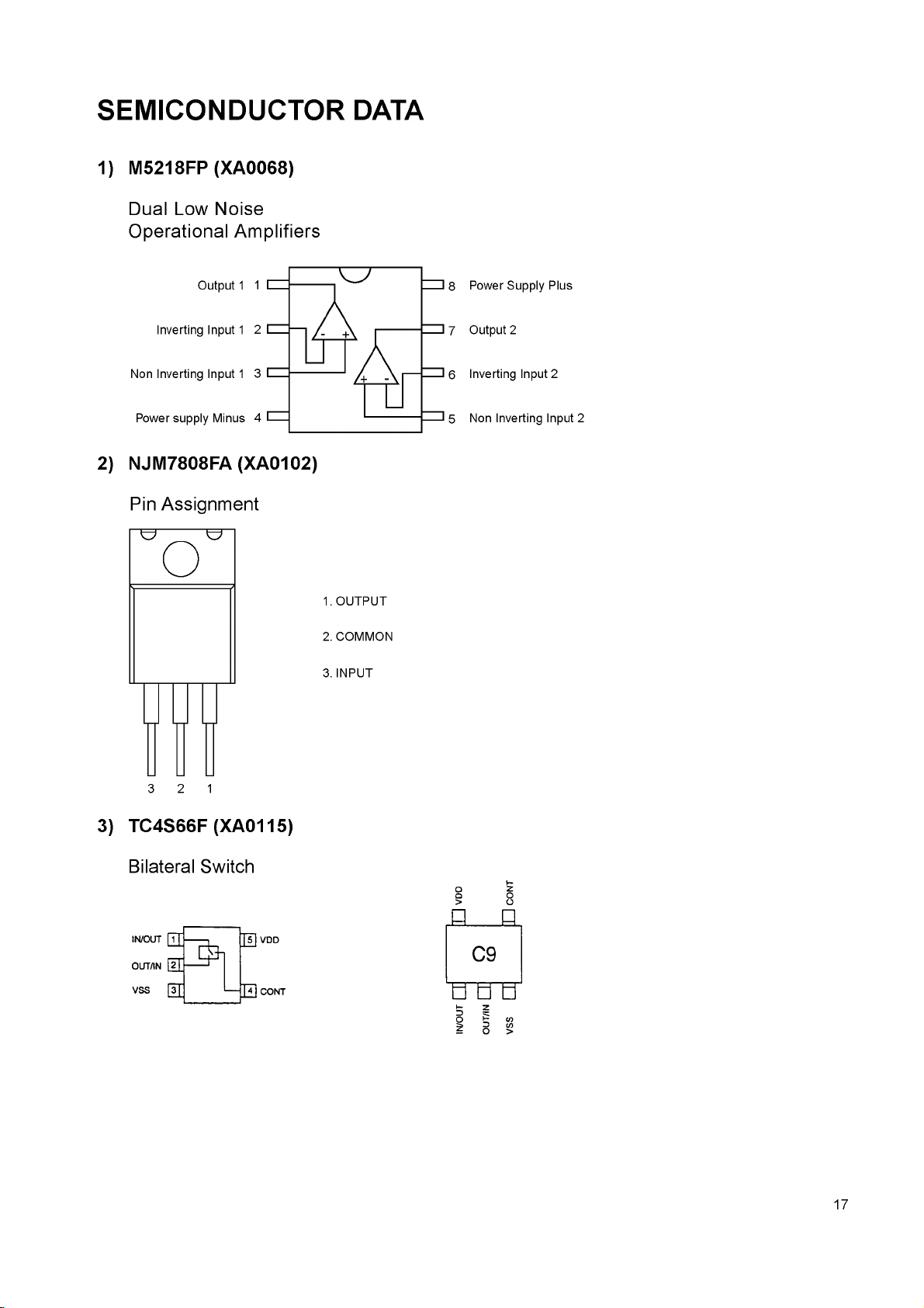
1) M5218FP (XA0068)............................................................................. 17
2) NJM7808FA (XA0102)........................................................................ 17
3) TC4S66F (XA0115)............................................................................. 17
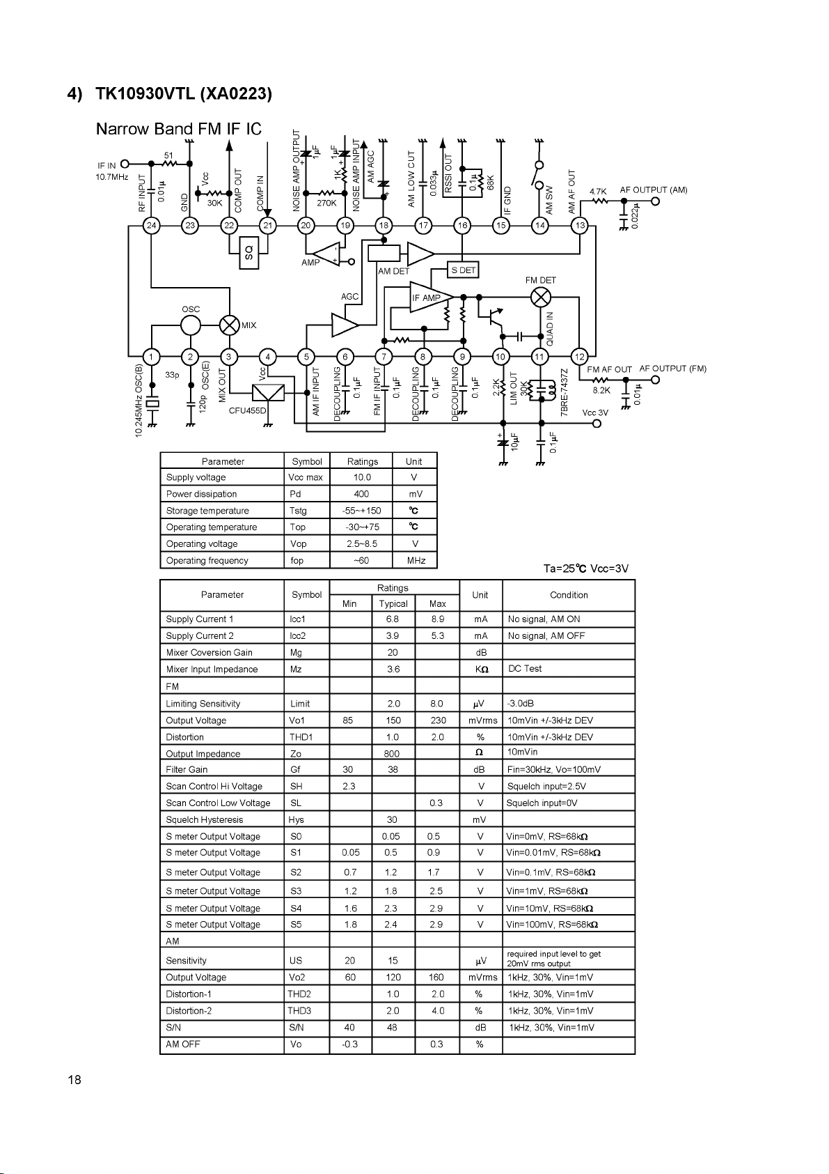
4) TK10930VTL (XA0223) ...................................................................... 18
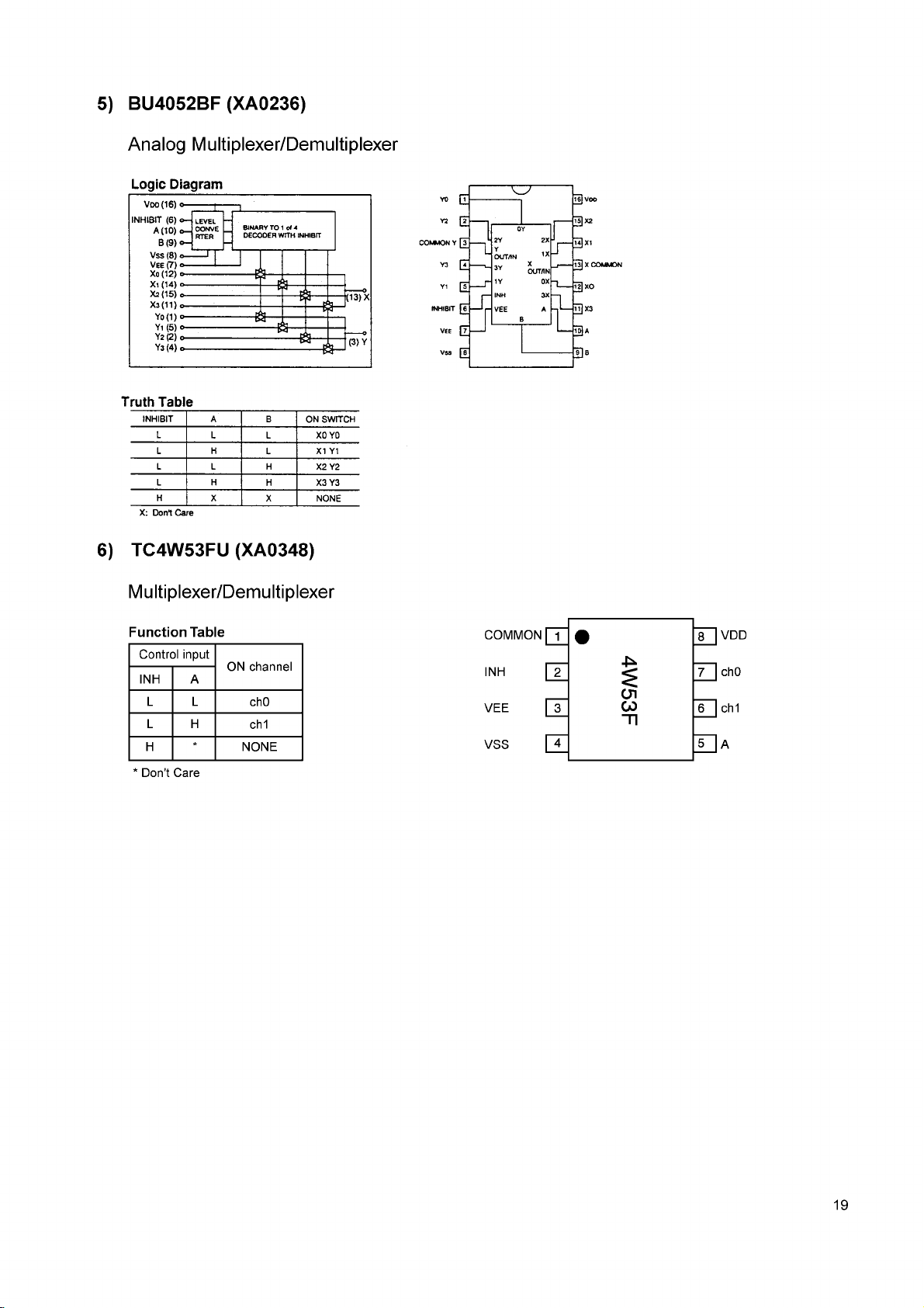
5) BU4052BF (XA0236)........................................................................... 19
6) TC4W53FU (XA0348) ........................................................................ 19
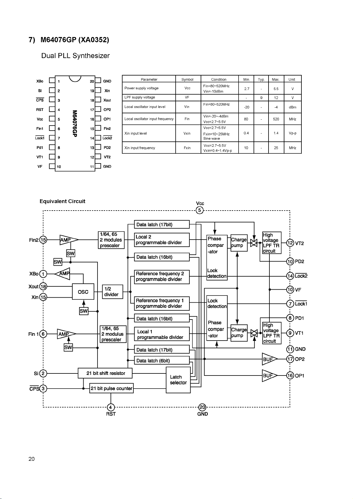
7) M64076GP (XA0352) .......................................................................... 20
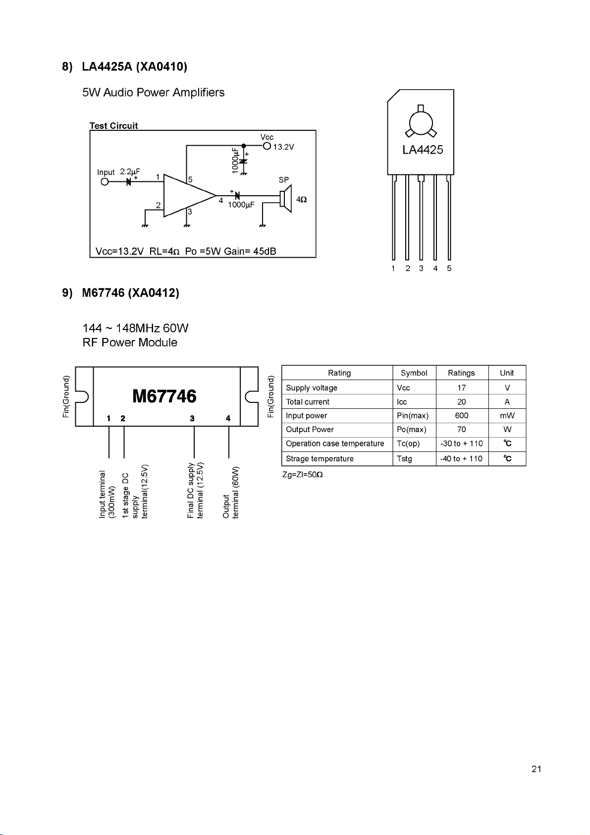
8) LA4425A (XA0410).............................................................................. 21
9) M67746 (XA0412) ............................................................................... 21
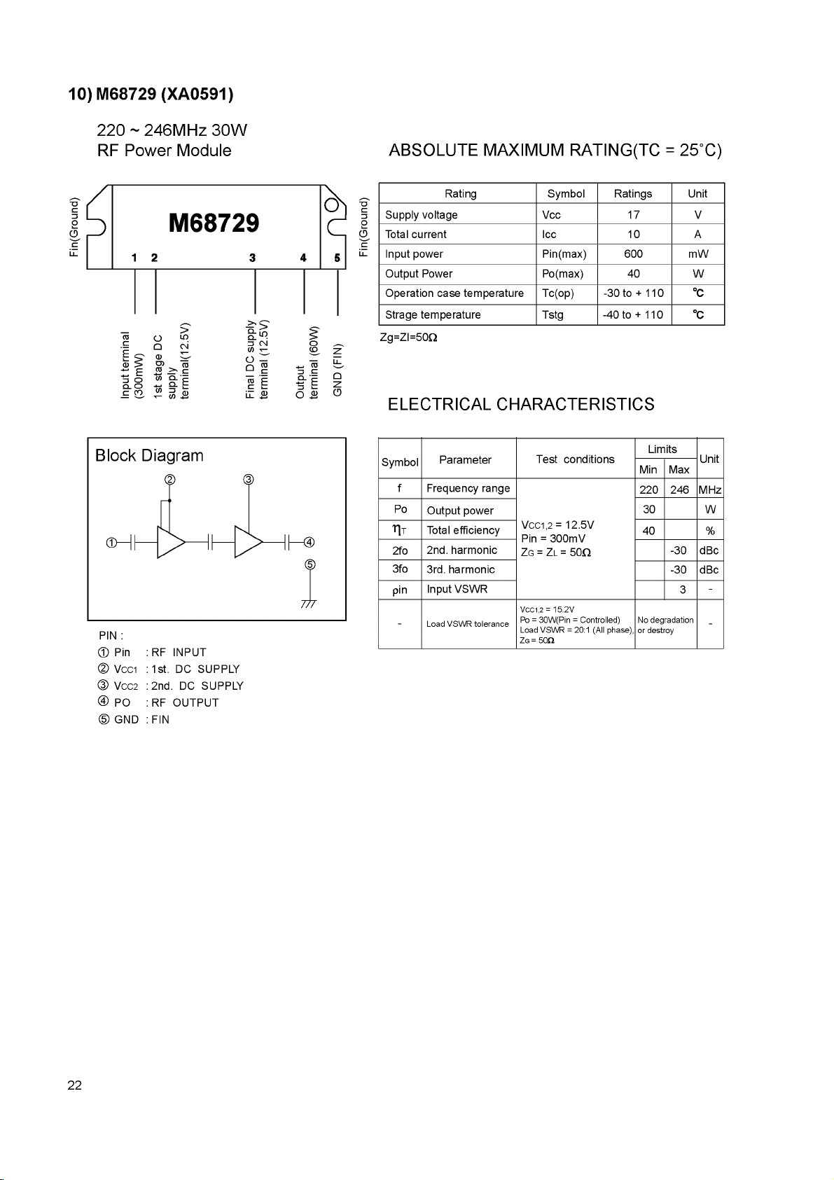
10) M68729 (XA0591) ............................................................................... 22
11) M57788 (XA0077A)............................................................................. 23
12) mPC2710T (XA0449) .......................................................................... 24
13) NJM2902 (XA0596)............................................................................. 24
14) 24LC32A (XA0604) ............................................................................. 25
15) S-80845ALMP-EA9-T2 (XA0620) ...................................................... 25
16) L88MS05TLL (XA0675)...................................................................... 25
17) AN8010M (XA0119) ............................................................................26
18) TK10489M (XA0314)........................................................................... 26
19) Transistor, Diode, and LED Ontline Drawings.................................... 27
20) LCD Connection (TTR3626UPFDHN) ............................................. 28
EXPLODED VIEW
1) Top and Front View.............................................................................. 29
2) Bottom View..........................................................................................30
3) LCD Assembly.....................................................................................31
PARTS LIST
CPU ................................................................................................32, 33
Main Unit(DR-135)........................................................................ 33~36
Main Unit(DR-235)........................................................................ 36~39
VCO Unit(DR-235) ............................................................................. 39
Main Unit(DR-435)............................................................................... 42
VCO Unit(DR-435) ............................................................................. 42
11,12
Mechanical Parts.................................................................................43
Packing Parts ...................................................................................... 43
ACCESSORIES................................................................................... 43
ACCESSORIES(SCREWSET) ......................................................... 43
TNC(EJ41U) ....................................................................................... 44
TNC (EJ41U) Packing Parts...............................................................45
DR-135 ADJUSTMENT
1) Adjustment Spot .................................................................................46
2) VCO and RX Adjustment Specification .............................................47
3) Tx Adjustment Specification................................................................ 47
4) Rx Test Specification............................................................................48
5) Tx Test Specification............................................................................49
DR-235 ADJUSTMENT
1) Adjustment Spot .................................................................................50
2) VCO and RX Adjustment Specification .............................................51
3) Tx Adjustment Specification................................................................ 51
4) Rx Test Specification............................................................................52
5) Tx Test Specification............................................................................53
DR-435 ADJUSTMENT
1) Adjustment Spot .................................................................................54
2) VCO and RX Adjustment Specification .............................................55
3) Tx Adjustment Specification................................................................ 55
4) Rx Test Specification............................................................................56
5) Tx Test Specification............................................................................57
PC BOARD VIEW
1) CPU Unit Side A ..................................................................................58
2) CPU Unit Side B ..................................................................................58
3) Main Unit Side A DR-135 (UP 0400B)................................................59
4) Main Unit Side B DR-135 (UP 0400B)................................................59
5) Main Unit Side A DR-235 (UP 0414)..................................................60
6) Main Unit Side B DR-235 (UP 0414)..................................................60
7) Main Unit Side A DR-435 (UP 0415)..................................................61
8) Main Unit Side B DR-435 (UP 0415)..................................................61
9) Tnc Unit Side A (UP 0402) (DR-135TP only) .................................... 62
10) Tnc Unit Side B (UP 0402) (DR-135TP only) .................................... 62
SCHEMATIC DIAGRAM
1) CPU Unit DR-135 / DR-235 / DR-435 ................................................ 63
2) Main Unit DR-135................................................................................ 64
3) Main Unit DR-235 ................................................................................ 65
4) Main Unit DR-435 ................................................................................ 66
5) TNC Unit (DR-135TP only)................................................................67
BLOCK DIAGRAM
1) DR-135................................................................................................. 68
2) DR-235................................................................................................. 69
3) DR-435................................................................................................. 70
A L I N C O , I N C .
Page 2

SPECIFICATIONS
■ General
Frequency coverage DR-135 DR-235 DR-435
T,TG
(U.S amateur)
E,EG
(European amateur)
TA,TAG
(Commercial)
118.000 ~ 135.995MHz (AM RX)
136.000 ~ 173.995MHz (RX)
144.000 ~ 147.995MHz (TX)
144.000 ~ 145.995MHz (RX.TX) 430.000 ~ 439.995MHz (RX.TX)
118.000 ~ 135.995MHz (AM RX)
136.000 ~ 173.995MHz (RX.TX)
216.000 ~ 279.995MHz (RX)
222.000 ~ 224.995MHz (TX)
350.000 ~ 511.995MHz (RX)
430.000 ~ 449.995MHz (TX)
Operating mode
Frequency resolution 5,8.33,10,12.5,15,20,25,30,50 KHz
Number of memory
channels
Antenna impedance
Power requirement 13.8V DC ±15% (11.7 to 15.8V)
Ground method Negative ground
Current drain Receive
Transmit
Operating temperature - 10”C to 60C
Frequency stability ±5ppm
Dimensions 142(w)x40(h)x174(d) mm
Weight Approx. 1.0kg
11.0A max. |8.0A max. |10.0A max.
FM 16K0F3E (Wide mode) 8K50F3E (Narrow mode)
100
5 0 '1 unbalanced
0.6A(Max.) 0.4A(Squelched)
( 142x40x188mm for projection included)
■ Transmitter
Output power High:50W (144-148MHz)
More than 33W (136-174MHz)
Mid:10W Mid:10W Mid:10W
Low:Approx.5W Low:Approx.5W Low:Approx.5W
Modulation system
Maximum frequency
deviation
Spurious emission -60dB
Adjacent
channel power
Noise and hum ratio -40dB (Wide mode) -34dB (Narrow mode)
Microphone impedance
High:25W High:35W
Variable reactance frequency modulation
±5kHz (Wide mode) ±2.5kHz (Narrow mode)
-60dB
2kfl
■ Receiver
Sensitivity
Receiver circuitry
Intermediate
frequency
Squelch sensitivity
Adjacent channel
selectivity
Intermoduration
rejection ratio
Spurious and
image rejection ratio
Audio output power
2
-16dBu for 12dB SINAD
Double conversion superheterodyne
1st 21.7MHz 2nd 450kHz 1st 30.85MHz 2nd 455kHz 1st 30.85MHz 2nd 455kHz
-18dBu
-65dB(Wide mode) -55dB(Narrow mode)
60dB
70dB
2.0W (8-J,10%THD)
! Note: All specifications are subject to change without notice or obligation.
Page 3
CIRCUIT DESCRIPTION DR-135/DR-235/DR-435
1) Receiver System (DR-135)
The receiver system is a double superheterodyne system with a 21.7 MHz first IF and a 450 kHz second IF
1. Front End
The received signal at any frequency in the 136.000MHz to 173.995MHz range
is passed through the low-pass filter (L116, L115, L114, L113, C204, C203,
C202, C216 and C215) and tuning circuit (L105, L104 and D105, D104), and
amplified by the RF amplifier (Q107). The signal from Q107 is then passed
through the tuning circuit (L103, L102, and varicaps D103 and D102) and
converted into 21.7 MHz by the mixer (Q106). The tuning circuit, which
consists of L105, L104, varicaps D105 and D104, L103, L102, varicaps
D103 and D102, is controlled by the tracking voltage form the VCO. The local signal
from the VCO is passed through the buffer (IC112), and supplied to the source of
the mixer (Q106). The radio uses the lower side of the superheterodyne system.
2. IF Circuit
The mixer mixes the received signal with the local signal to obtain the sum of
and difference between them. The crystal filter (XF102, XF101) selects 21.7
MHz frequency from the results and eliminates the signals of the unwanted
frequencies. The first IF amplifier (Q105) then amplifies the signal of the selected
frequency.
3. Demodulator Circuit
4. Audio Circuit
After the signal is amplified by the first IF amplifier (Q105), it is input to pin 24 of
the demodulator IC (IC108). The second local signal of 21.25 MHz (shared
with PLL IC reference oscillation), which is oscillated by the internal oscillation
circuit in IC116 and crystal (X103), is input through pin 1 of IC108. Then, these
two signals are mixed by the internal mixer in IC108 and the result is converted
into the second IF signal with a frequency of 450 kHz. The second IF signal is
output from pin 3 of IC108 to the ceramic filter (FL101 or FL102), where the
unwanted frequency band of that signal is eliminated, and the resulting signal
is sent back to the IC108 through pins 5.
The second IF signal input via pin 5 is demodulated by the internal limiter
amplifier and quadrature detection circuit in IC108, and output as an audio
signal through pin 12.
The audio signal from pin 12 of IC108 is amplified by the audio amplifier
(IC104:A),and switched by the signal switch IC (IC111) and then input it to the
de-emphasis circuit.
and is compensated to the audio frequency characteristics in the de-emphasis
circuit (R203, R207, R213, R209, C191, C218, C217) and amplified by the AF
amplifier (IC104:D). The signal is then input to volume (VR1) . The adjusted signal is
sent to the audio power amplifier (IC117) through pin 1 to drive the speaker.
3
Page 4
5. Squelch Circuit
The detected output which is outputted from the pin 12 of IC108 is inputted to
pin 19 of IC108 after it was been amplified by IC104:A and it is outputted from
pin 20 after the noise component was been eliminated from the composed
band pass filter in the built in amplifier of the IC, then the signal is rectified by
D106 to convert into DC component. The adjusted voltage level at VR101 is
delivered to the comparator of the CPU.
The voltage is led to pin 2 of CPU and compared with the setting voltage. The
squelch will open if the input voltage is lower than the setting voltage.
During open squelch, pin 30 (SQC) of the CPU becomes "L" level, AF control
signal is being controlled and sounds is outputted from the speaker.)
6. AIR Band Reception(T only)
When the frequency is within 118~135.995MHz, Q110 automatically turns ON,
pin 14 of IC108 becomes "L" level and the condition becomes in AM detection
mode.
The receiver signal passed through the duplexer is let to the antenna switch
(D107,D101). After passing through the band-pass filter, the signal is amplified
by RF amplifier Q112. Secondly the signal is mixed with the signal from the first
local oscillator in the first-mixer Q106,then converted into the first IF. Its unwanted
signal is let to IC106, pin24. Then converted into the second IF. and is demodulated
by AM decoder of IC106, and is output from pin13 as the AF signal.
7. WIDE/NARROW switching circuit
The 2nd IF 450 kHz signal which passes through filter FL101 (wide) and FL102
(narrow) during narrow, changes its width using the width control switching
IC103 and IC102.
2) Transmitter System (DR-135)
1. Modulator Circuit
The audio signal is converted to an electrical signal by the microphone, and
input it to the microphone amplifier (Q6). Amplified signal which passes through
mic-mute control IC109 is adjusted to an appropriate mic-volume by means of
mic-gain adjust VR106.
IC114:A and B consists of two operational amplifiers; one amplifier (pins 1, 2,
and 3) is composed of pre-emphasis and IDC circuits and the other (pins 5, 6,
and 7) is composed of a splatter filter. The maximum frequency deviation is
obtained by VR107. and input to the signal switch (IC113) (9600 bps packet
signal input switch) and input to the cathode of the varicap of the VCO, to
change the electric capacity in the oscillation circuit. This produces the frequency
modulation.
4
Page 5
2. Power Amplifier Circuit
The transmitted signal is oscillated by the VCO, amplified by the drive amplifier
(IC112) and younger amplifier (Q115), and input to the final power module
(IC110). The signal is then amplified by the final power module (IC110) and led
to the antenna switch (D110) and low-pass filter (L113, L114, L115, L116,
C215, C216, C202, C203 and C204), where unwanted high harmonic waves
are reduced as needed, and the resulting signal is supplied to the antenna.
3. APC Circuit
Part of the transmission power from the low-pass filter is detected by D111 and
D112, converted to DC. The detection voltage is passed through the APC circuit
(Q118, Q117, Q116), then it controls the APC voltage supplied to the younger
amplifier Q115 and the final power module IC110 to fix the transmission power.
3) PLL Synthesizer Circuit (DR-135)
1. PLL
The dividing ratio is obtained by sending data from the CPU (IC1) to pin 2 and
sending clock pulses to pin 3 of the PLL IC (IC116). The oscillated signal from
the VCO is amplified by the buffer (Q134 and Q135) and input to pin 15 of
IC116. Each programmable divider in IC116 divides the frequency of the input
signal by N according to the frequency data, to generate a comparison frequency of
5 or 6.25 kHz.
2. Reference Frequency Circuit
The reference frequency appropriate for the channel steps is obtained by dividing
the 21.25 MHz reference oscillation (X103) by 4250 or 3400, according to the data
from the CPU (IC1). When the resulting frequency is 5 kHz, channel steps of 5,
10, 15, 20, 25, 30, and 50 kHz are used. When it is 6.25 kHz, the 12.5 kHz
channel step is used.
3. Phase Comparator Circuit
The PLL (IC116) uses the reference frequency, 5 or 6.25kHz. The phase
comparator in the IC116 compares the phase of the frequency from the VCO
with that of the comparison frequency, 5 or 6.25kHz, which is obtained by the
internal divider in IC116.
4. PLL Loop Filter Circuit
If a phase difference is found in the phase comparison between the reference
frequency and VCO output frequency, the charge pump output (pin 13) of IC116
generates a pulse signal, which is converted to DC voltage by the PLL loop
filter and input to the varicap of the VCO unit for oscillation frequency control.
5
Page 6
5. VCO Circuit
A Colpitts oscillation circuit driven by Q131 directly oscillates the desired frequency.
The frequency control voltage determined in the CPU (IC1) and PLL circuit is
input to the varicaps (D122 and D123). This change the oscillation frequency,
which is amplified by the VCO buffer (Q134) and output from the VCO area.
6. VCO Shift Circuit
During transmission or the AIR band Reception (118~136 MHz), the VCO shift
circuit turns ON Q138, change control the capacitance of L123 and safely
oscillates the VCO by means of H signal from pin 16 of IC116.)
4) Receiver System (DR-235)
The receiver system is a double superheterodyne system with a 30.85 MHz first IF and a 455 kHz second IF.
1. Front End
The received signal at any frequency in the 216.000MHz to 279.995MHz range
is passed through the low-pass filter (L116, L115, L114, L113, C204, C203,
C202, C216 and C215) and tuning circuit (L105, L104 and D105, D104), and
amplified by the RF amplifier (Q107). The signal from Q107 is then passed
through the tuning circuit (L103, L107, L102, and varicaps D103, D107 and
D102) and converted into 30.85 MHz by the mixer (Q106). The tuning circuit,
which consists of L105, L104, varicaps D105 and D104, L103, L107, L102,
varicaps D103, D107 and D102, is controlled by the tracking voltage form the
VCO. The local signal from the VCO is passed through the buffer (Q112), and
supplied to the source of the mixer (Q106). The radio uses the lower side of the
superheterodyne system.
2. IF Circuit
3. Demodulator Circuit
The mixer mixes the received signal with the local signal to obtain the sum of
and difference between them. The crystal filter (XF102, XF101) selects 30.85
MHz frequency from the results and eliminates the signals of the unwanted
frequencies. The first IF amplifier (Q105) then amplifies the signal of the selected
frequency.
After the signal is amplified by the first IF amplifier (Q105), it is input to pin 24 of
the demodulator IC (IC108). The second local signal of 30.395 MHz, which is
oscillated by the internal oscillation circuit in IC108 and crystal (X104), is input
through pin 1 of IC108. Then, these two signals are mixed by the internal mixer
in IC108 and the result is converted into the second IF signal with a frequency
of 455 kHz. The second IF signal is output from pin 3 of IC108 to the ceramic
filter (FL101 or FL102), where the unwanted frequency band of that signal is
eliminated, and the resulting signal is sent back to the IC108 through pins 5.
The second IF signal input via pin 5 is demodulated by the internal limiter
amplifier and quadrature detection circuit in IC108, and output as an audio
signal through pin 12.
6
Page 7
4. Audio Circuit
5. Squelch Circuit
The audio signal from pin 12 of IC108 is amplified by the audio amplifier
(IC104:A), and switched by the signal switch IC (IC111) and then input it to the
de-emphasis circuit.
and is compensated to the audio frequency characteristics in the de-emphasis
circuit (R203, R207, R213, R209, C191, C218, C217) and amplified by the AF
amplifier (IC104:D). The signal is then input to volume (VR1) . The adjusted
signal is sent to the audio power amplifier (IC117) through pin 1 to drive the
speaker.
The detected output which is outputted from the pin 12 of IC108 is inputted to
pin 19 of IC108 after it was been amplified by IC104:A and it is outputted from
pin 20 after the noise component was been eliminated from the composed
band pass filter in the built in amplifier of the IC, then the signal is rectified by
D106 to convert into DC component. The adjusted voltage level at VR101 is
delivered to the comparator of the CPU.
The voltage is led to pin 2 of CPU and compared with the setting voltage. The
squelch will open if the input voltage is lower than the setting voltage.
During open squelch, pin 30 (SQC) of the CPU becomes "L" level, AF control
signal is being controlled and sounds is outputted from the speaker.)
6. AIR Band Reception(T only)
If it is made air band receiving mode, IF signal is demodulated by AM decoder
of IC106, and is output from pin13 as the AF signal.
7. WIDE/NARROW switching circuit
The 2nd IF 455 kHz signal which passes through filter FL101 (wide) and FL102
(narrow) during narrow, changes its width using the width control switching
IC103 and IC102.
5) Transmitter System (DR-235)
1. Modulator Circuit
The audio signal is converted to an electrical signal by the microphone, and
input it to the microphone amplifier (Q6). Amplified signal which passes through
mic-mute control IC109 is adjusted to an appropriate mic-volume by means of
mic-gain adjust VR106.
IC114:A and B consists of two operational amplifiers; one amplifier (pins 1, 2,
and 3) is composed of pre-emphasis and IDC circuits and the other (pins 5, 6,
and 7) is composed of a splatter filter. The maximum frequency deviation is
obtained by VR107. and input to the signal switch (IC113) (9600 bps packet
signal input switch) and input to the cathode of the varicap of the VCO, to
change the electric capacity in the oscillation circuit. This produces the frequency
modulation.
7
Page 8
2. Power Amplifier Circuit
The transmitted signal is oscillated by the VCO, amplified by the drive amplifier
(IC112) and younger amplifier (Q115), and input to the final power module
(IC110). The signal is then amplified by the final power module (IC110) and led
to the antenna switch (D110) and low-pass filter (L113, L114, L115, L116,
C215, C216, C202, C203 and C204), where unwanted high harmonic waves
are reduced as needed, and the resulting signal is supplied to the antenna.
3. APC Circuit
Part of the transmission power from the low-pass filter is detected by D111
and D112, converted to DC. The detection voltage is passed through the
APC circuit (Q118, Q117, Q116), then it controls the APC voltage supplied to
the younger amplifier Q115 and the final power module IC110 to fix the
transmission power.
6) PLL Synthesizer Circuit (DR-235)
1. PLL
The dividing ratio is obtained by sending data from the CPU (IC1) to pin 2 and
sending clock pulses to pin 3 of the PLL IC (IC501). The oscillated signal from
the VCO is amplified by the buffer (Q504 and Q501) and input to pin 15 of
IC501. Each programmable divider in IC501 divides the frequency of the input
signal by N according to the frequency data, to generate a comparison frequency of
5 or 6.25 kHz.
2. Reference Frequency Circuit
The reference frequency appropriate for the channel steps is obtained by
dividing the 12.8 MHz reference oscillation (X103) by 2560 or 2048, according
to the data from the CPU (IC1). When the resulting frequency is 5 kHz, channel
steps of 5, 10, 15, 20, 25, 30, and 50 kHz are used. When it is 6.25 kHz, the
12.5 kHz channel step is used.
3. Phase Comparator Circuit
The PLL (IC501) uses the reference frequency, 5 or 6.25kHz. The phase
comparator in the IC501 compares the phase of the frequency from the VCO
with that of the comparison frequency, 5 or 6.25kHz, which is obtained by the
internal divider in IC501.
4. PLL Loop Filter Circuit
If a phase difference is found in the phase comparison between the reference
frequency and VCO output frequency, the charge pump output (pin 13) of IC501
generates a pulse signal, which is converted to DC voltage by the PLL loop
filter and input to the varicap of the VCO unit for oscillation frequency control.
8
Page 9
5. VCO Circuit
A Colpitts oscillation circuit driven by Q503 directly oscillates the desired frequency.
The frequency control voltage determined in the CPU (IC1) and PLL circuit is
input to the varicaps (D503 and D504). This change the oscillation frequency,
which is amplified by the VCO buffer (Q504) and output from the VCO area.
7) Receiver System (DR-435)
The receiver system is a double superheterodyne system with a 30.85 MHz first IF and a 455 kHz second IF.
1. Front End
The received signal at any frequency in the 430.00MHz to 439.995MHz range
is passed through the low-pass filter (L115, L114, L116, C204, C203, C202,
C216 and C215) and amplified by the RF amplifier (Q107). The signal from
Q107 is then passed through the BPF circuit (L103, L102) and converted into
30.85 MHz by the mixer (Q106). The local signal from the VCO is passed
through the buffer (Q503,Q504), and supplied to the source of the mixer (Q106).
The radio uses the lower side of the superheterodyne system.
2. IF Circuit
The mixer mixes the received signal with the local signal to obtain the sum of
and difference between them. The crystal filter (XF101) selects 30.85MHz frequency
from the results and eliminates the signals of the unwanted frequencies. The first IF
amplifier (Q105) then amplifies the signal of the selected frequency.
3. Demodulator Circuit
4. Audio Circuit
After the signal is amplified by the first IF amplifier (Q105), it is input to pin 20 of
the demodulator IC (IC108). The second local signal of 30.85MHz (Crystal
oscillator) is input pin 1 of IC108. Then, these two signals are mixed by the
internal mixer in IC108 and the result is converted into the second IF signal
with a frequency of 455 kHz. The second IF signal is output from pin 4 of IC108
to the ceramic filter (FL101 or FL102), where the unwanted frequency band of
that signal is eliminated, and the resulting signal is sent back to the IC108
through pins 6.
The second IF signal input via pin 6 is demodulated by the internal limiter
amplifier and quadrature detection circuit in IC108, and output as an audio
signal through pin 11.
The audio signal from pin 11 of IC108 is amplified by the audio amplifier
(IC104:A), and switched by the signal switch IC (IC111) and then input it to the
de-emphasis circuit.
and is compensated to the audio frequency characteristics in the de-emphasis
circuit (R203, R207, R213, R209, C191, C218, C217) and amplified by the AF
amplifier (IC104:D). The signal is then input to volume (VR1) . The adjusted
signal is sent to the audio power amplifier (IC117) through pin 1 to drive the
speaker.
9
Page 10
5. Squelch Circuit
The detected output which is outputted from the pin 11 of IC108 is inputted to
pin 13 of IC108 after it was been amplified by IC104:A and it is outputted from
pin 14 after the noise component was been eliminated from the composed
band pass filter in the built in amplifier of the IC, then the signal is rectified by
D106 to convert into DC component. The adjusted voltage level at VR101 is
delivered to the comparator of the CPU.
The voltage is led to pin 2 of CPU and compared with the setting voltage. The
squelch will open if the input voltage is lower than the setting voltage.
During open squelch, pin 30 (SQC) of the CPU becomes "L" level, AF control
signal is being controlled and sounds is outputted from the speaker.
6. WIDE/NARROW switching circuit
The 2nd IF 455 KHz signal which passes through filter FL101 (wide) and FL102
(narrow) during narrow, changes its width using the width control switching
IC103 and IC102.
8) Transmitter System (DR-435)
1. Modulator Circuit
The audio signal is converted to an electrical signal by the microphone, and
input it to the microphone amplifier (Q6). Amplified signal which passes through
mic. mute control IC109 is adjusted to an appropriate mic. volume by means of
mic. gain adjust VR106.
IC114:A and B consists of two operational amplifiers; one amplifier (pins 1, 2,
and 3) is composed of pre-emphasis and IDC circuits and the other (pins 5, 6,
and 7) is composed of a splatter filter. The maximum frequency deviation is
obtained by VR107. and input to the signal switch (IC113) (9600 bps packet
signal input switch) and input to the cathode of the varicap of the VCO, to
change the electric capacity in the oscillation circuit. This produces the frequency
modulation.
2. Power Amplifier Circuit
The transmitted signal is oscillated by the VCO, amplified by the drive amplifier
(Q131, Q125) and younger amplifier (Q115), and input to the final power module
(IC110). The signal is then amplified by the final power module (IC110) and led
to the antenna switch (D110) and low-pass filter (L116, L114, L115, C215,
C216, C202, C203 and C204), where unwanted high harmonic waves are
reduced as needed, and the resulting signal is supplied to the antenna.
3. APC Circuit
10
Part of the transmission power from the low-pass filter is detected by D111 and
D112, converted to DC. The detection voltage is passed through the APC
circuit(Q118, Q117, Q116), then it controls the APC voltage supplied to the
younger amplifier Q115 and the final power module IC110 to fix the transmission
power.
Page 11
9) PLL Synthesizer Circuit (DR-435)
1. PLL
The dividing ratio is obtained by sending data from the CPU (IC1) to pin 2 and
sending clock pulses to pin 3 of the PLL IC (IC501). The oscillated signal from
the VCO is amplified by the buffer (Q503 and Q501) and input to pin 15 of
IC501. Each programmable divider in IC501 divides the frequency of the input
signal by N according to the frequency data, to generate a comparison frequency of
5 or 6.25 kHz.
2. Reference Frequency Circuit
The reference frequency appropriate for the channel steps is obtained by dividing
the 21.25 MHz reference oscillation (X103) by 4250 or 3400, according to the
data from the CPU (IC1). When the resulting frequency is 5 kHz, channel steps
of 5, 8.33, 10, 15, 20, 25, 30, and 50 kHz are used. When it is 6.25 kHz, the 12.5
kHz channel step is used.
3. Phase Comparator Circuit
The PLL (IC501) uses the reference frequency, 5 or 6.25kHz. The phase
comparator in the IC501 compares the phase of the frequency from the VCO
with that of the comparison frequency, 5 or 6.25kHz, which is obtained by the
internal divider in IC501.
4. PLL Loop Filter Circuit
If a phase difference is found in the phase comparison between the reference
frequency and VCO output frequency, the charge pump output (pin 13) of IC501
generates a pulse signal, which is converted to DC voltage by the PLL loop
filter and input to the varicap of the VCO unit for oscillation frequency control.
5. VCO Circuit
A Colpitts oscillation circuit driven by Q502 directly oscillates the desired frequency.
The frequency control voltage determined in the CPU (IC1) and PLL circuit is
input to the varicaps (D502 and D503). This change the oscillation frequency,
which is amplified by the VCO buffer (Q503,504) and output from the VCO unit.
10) CPU and Peripheral Circuits (DR-135 DR-235 DR-435)
1. LCD Display Circuit
The CPU turns ON the LCD via segment and common terminals with 1/4 the
duty and 1/3 the bias, at the frame frequency is 64Hz.
11
Page 12
2. Dimmer Circuit
3. Reset and Backup
4. S(Signal) Meter Circuit
5. DTMF Encoder
The dimmer circuit makes the output of pin 13 of CPU (IC1) into "H" level at set
mode, so that Q9 and Q3 will turn ON to make the lamp control resistor R84
short and make its illumination bright. But on the other hand, if the dimmer
circuit makes pin 13 into "L" level, Q9 and Q3 will turn OFF, R84's illumination
will become dimmer as its hang on voltage falls down in the working LED (D11,
D2, D5, D3 and D6).
When the power form the DC cable increases from Circuits 0 V to 2.5 or more,
"H" level reset signal is output form the reset IC (IC4) to pin 33 of the CPU
(IC1), causing the CPU to reset. The reset signal, however, waits at 100, and
does not enter the CPU until the CPU clock (X1) has stabilized.
The DC potential of pin 16 of IC106 is input to pin 1 of the CPU (IC1), converted
from an analog to a digital signal, and displayed as the S-meter signal on the
LCD.
The CPU (IC1) is equipped with an internal DTMF encoder. The DTMF signal
is output from pin 10, through R35, R34 and R261 (for level adjustment), and
then through the microphone amplifier (IC114:A), and is sent to the varicap of
the VCO for modulation. At the same time, the monitoring tone passes through
the AF circuit and is output form the speaker.
6. Tone Encoder
7. DCS Encoder
8. CTCSS, DCS Decoder
The CPU (IC1) is equipped with an internal tone encoder. The tone signal (67.0
to 250.3 Hz) is output from pin 9 of the CPU to the varicap (D122 and D123) of
the VCO for modulation.
The CPU (IC1) is equipped with an internal DCS code encoder. The code
(023 to 754) is output from pin 9 of the CPU to the varicap (D124) of the
PLL reference oscillator. When DCS is ON, DCS MUTE circuit (Q126-ON,
Q133-ON, Q132-OFF) works. The modulation activates in X103 side only.
The voice band of the AF output signal from pin 1 of IC104:A is cut by sharp
active filter IC104:B and C (VCVS) and amplified, then led to pin 4 of CPU. The
input signal is compared with the programmed tone frequency code in the
CPU. The squelch will open when they match. During DCS, Q108 is ON, C156
is working and cut off frequency is lowered.
12
Page 13
11) Power Supply Circuit
When power supply is ON, there is a "L" signal being inputted to pin 39 (PSW) of CPU which enables
the CPU to work.
Then, "H" signal is outputted from the pin 41 (C5C) of CPU and drives ON the power supply switch
control Q8 and Q7 which turns the 5VS ON.
5VS turns ON the PLL IC116, main power supply switch Q127 and Q122, AF POWER IC117 and the
8 V of AVR (IC115).
During reception, pin 29 (R5) of CPU outputs "H" level, Q124 is ON, and the reception circuits supplied by 8 V.
While during transmission, pin 28 (T5) of CPU outputs "L" level which is reverse by Q11 so that the output
in Q128 will be "H" level, Q123 is ON, and the transmission circuit is supplied by 8 V.
Or, in the case when the condition of PLL is UNLOCK, "H" level is outputted from pin 14 of IC106,
UNLOCK switch Q129is ON, transmission switch Q128 is OFF which makes the transmission to stop.
1. ACC External Power Supply Terminal
When optional power supply cord DEC-37 etc. is connected to the external
power supply terminal JK101, with ACC power supply ON, switch Q101 will
turn ON, 5 V of AVR IC101 pin 2 (STB) becomes "L" which makes C5V to turn
ON. With this, it can turn the power supply of the radio ON.
13
Page 14
P67/ AN 7
P66/A N 6
P65/ AN 5
P6 4/ AN 4
P63/SC LK 22/A N3
P6 2/ SC LK 21/A N2
P6 1/SO UT 2/AN 1
P6 0/ SIN2/AN 0
P5 7/ AD T/ DA 2
P5 6/D A1
P5 5/C NTR1
P5 4/ CN TR 0
P5 3/R TP 1
P52/ RT P0
P5 1/PW M1
P5 0/PW M 0
P4 7/S RDY1
P4 6/S CL K1
P45/ TX D
P4 4/ RX D
P43 /0 /TOU T
P4 2/ INT2
P4 1/INT1
P4 0
P7 7
Page 15
! OOrrSSSSWmOOOOOOOOOOO = i!!:
‘ - * W W W O - A WW C/ )'n Oo -A WW ^Ü 10 >NO O( DO -i W
ñ S ö P > < ^ OTWCowwwwwOTMrnmm
îîtîtîîî
o
TI
<
m
CD1
3
5L
O
o
3
3
CD
a
o
3
I O
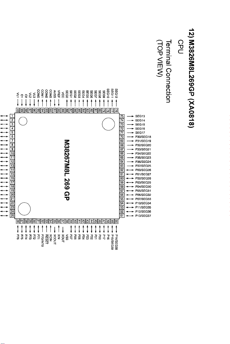
CPU
M3826M8L269GP (XA0818)
T ~
T
_3_
° o
X
I T
_6_
7_
T
_9_
_10
n
H
13
H
I I
16
JZ
Jb
3 1
20
21
22
23
n
v J
îîlîîlîîîlîl ÎHI1ÎÎÎ1Î1
"T3 U *0 "U "0 "O "O Ul XXXX<"DTJ'I]'DT3T)
O ) OH» » IO -* I
_l ^ 0 _ Q W M M M M M W
2
G O
0 0
I O
O )
-n |
0 0
r -
I O
O )
C D
G >
" ü
O c W '^ ° )Cr
K> '•* o *si O) oi £»■
v _ y
io 2 IS 2 2
W C/5
75]
------
► SEG 13
74]
------
► SE G 14
73|
------
► SEG 15
72~|
------
► SEG 16
7T]
------
► SE G 17
7Ö j
------
► P 30 /SEG 18
69]
------
► P 31/SE G 19
68]
------
► P32/SE G 20
67]
------
► P33/SEG21
66]
------
► P34/ SE G22
65]
------
► P35/SE G 23
64]
------
► P36/SE G 24
63]
------
► P37/SE G 25
62 ) - * — ► P 00 /SEG 26
6Ï1 ► P 01 /SEG 27
60] ► P 02 /SEG 28
59 ) ► P03/SE G 29
58] ► P0 4/SE G3 0
57] - *— ► P05/ SE G3 1
56 ) P0 6/SE G3 2
55} -«— ► P 07 /SEG 33
54] ► P10/SE G 34
53) P1 1/ SE G35
52] - * — ► P 12 /S EG 36
| J ] P 13 /S EG 37
Page 16
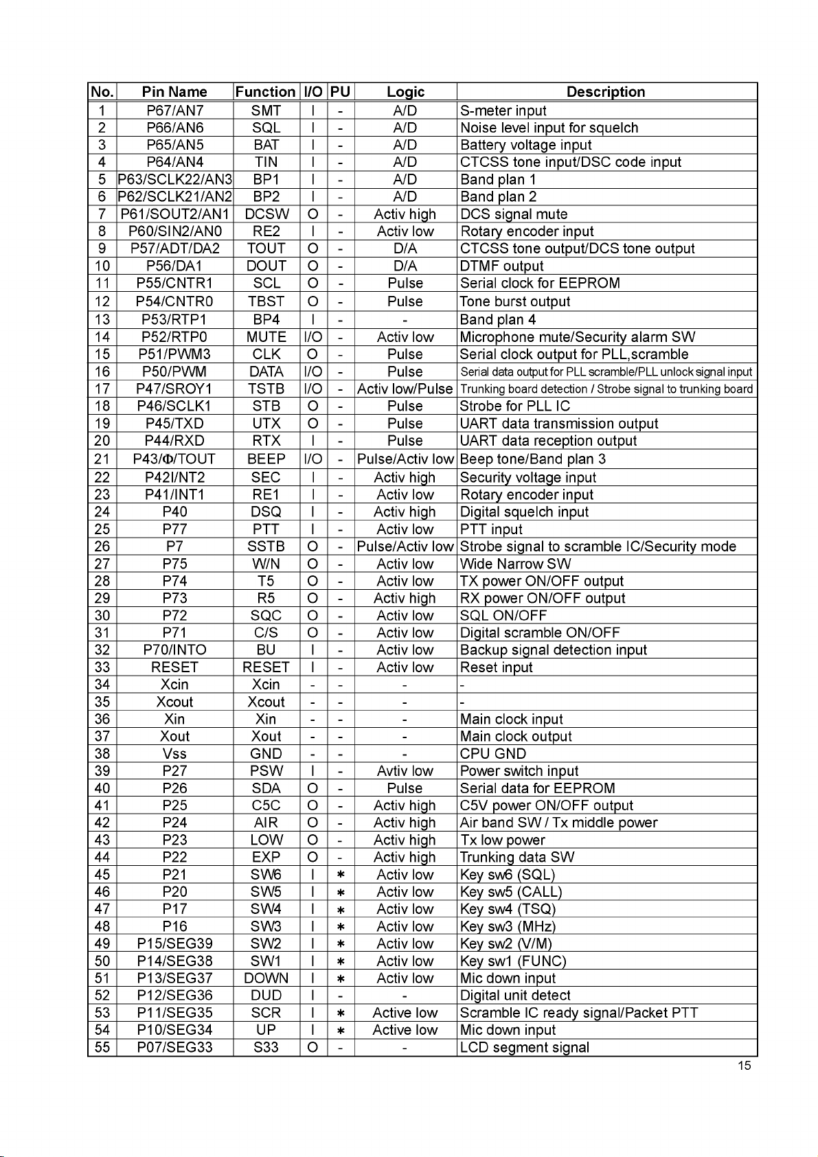
No. Pin Name Function I/O PU Logic Description
1 P67/AN7 SMT I
2 P66/AN6 SQL I
3 P65/AN5 BAT I
4 P64/AN4 TIN I
5 P63/SCLK22/AN3 BP1 I
6 P62/SCLK21/AN2 BP2 I
7 P61/SOUT2/AN1 DCSW O
8 P60/SIN2/AN0 RE2 I
9 P57/ADT/DA2 TOUT O
10 P56/DA1 DOUT O
11 P55/CNTR1 SCL O
12 P54/CNTR0 TBST O
13 P53/RTP1 BP4 I
14 P52/RTP0 MUTE I/O
15 P51/PWM3 CLK O
16 P50/PWM DATA I/O
17 P47/SROY1 TSTB I/O
18 P46/SCLK1 STB O
19 P45/TXD UTX O
20 P44/RXD RTX I
21 P43/®/TOUT BEEP I/O
22 P42I/NT2 SEC I
23 P41/INT1 RE1 I
24 P40 DSQ I
25 P77 PTT I
26 P7 SSTB O
27 P75 W/N O
28 P74 T5 O
29 P73 R5 O
30 P72 SQC O
31 P71 C/S O
32 P70/INT0 BU I
33 RESET RESET I
34 Xcin Xcin
35 Xcout Xcout
36 Xin Xin
37 Xout Xout
38 Vss GND
39 P27 PSW I
40 P26 SDA O
41 P25 C5C O
42 P24 AIR O
43 P23 LOW O
44 P22 EXP O
45 P21 SW6 I
46 P20 SW5 I
-
-
-
-
-
-
-
-
-
-
-
-
A/D S-meter input
A/D Noise level input for squelch
A/D Battery voltage input
A/D CTCSS tone input/DSC code input
A/D Band plan 1
A/D Band plan 2
Activ high DCS signal mute
Activ low Rotary encoder input
D/A CTCSS tone output/DCS tone output
D/A DTMF output
Pulse Serial clock for EEPROM
Pulse Tone burst output
- -
-
Activ low Microphone mute/Security alarm SW
-
-
-
-
-
-
-
-
-
-
-
-
-
-
-
-
-
-
-
Pulse Serial clock output for PLL,scramble
Pulse
Activ low/Pulse
Pulse Strobe for PLL IC
Pulse UART data transmission output
Pulse UART data reception output
Pulse/Activ low Beep tone/Band plan 3
Activ high Security voltage input
Activ low Rotary encoder input
Activ high Digital squelch input
Activ low PTT input
Pulse/Activ low Strobe signal to scramble IC/Security mode
Activ low Wide Narrow SW
Activ low TX power ON/OFF output
Activ high RX power ON/OFF output
Activ low SQL ON/OFF
Activ low Digital scramble ON/OFF
Activ low Backup signal detection input
Activ low Reset input
- - - -
- - - -
- - -
- - -
- - -
-
Avtiv low Power switch input
-
-
-
-
-
*
*
Pulse Serial data for EEPROM
Activ high C5V power ON/OFF output
Activ high Air band SW / Tx middle power
Activ high Tx low power
Activ high Trunking data SW
Activ low Key sw6 (SQL)
Activ low Key sw5 (CALL)
Band plan 4
Serial data output for PLL scramble/PLL unlock signal input
Trunking board detection / Strobe signal to trunking board
Main clock input
Main clock output
CPU GND
47 P17 SW4 I * Activ low Key sw4 (TSQ)
48 P16 SW3 I
49 P15/SEG39 SW2 I
50 P14/SEG38 SW1 I
51 P13/SEG37 DOWN I
52 P12/SEG36 DUD I
53 P11/SEG35 SCR I
54 P10/SEG34 UP I
*
Activ low Key sw3 (MHz)
*
Activ low
*
Activ low Key sw1 (FUNC)
*
Activ low Mic down input
- -
*
Active low Scramble IC ready signal/Packet PTT
*
Active low Mic down input
Key sw2 (V/M)
Digital unit detect
55 P07/SEG33 S33 O - - LCD segment signal
15
Page 17
No.
_56_
57
58
59
60
61
62
63
64
65
66
67
68
69
70
71
72
73
74
75
76
77
78
79
80
81
82
83
84
85
86
87
88
89
90
91
92
93
94
95
96
97
98
99
100
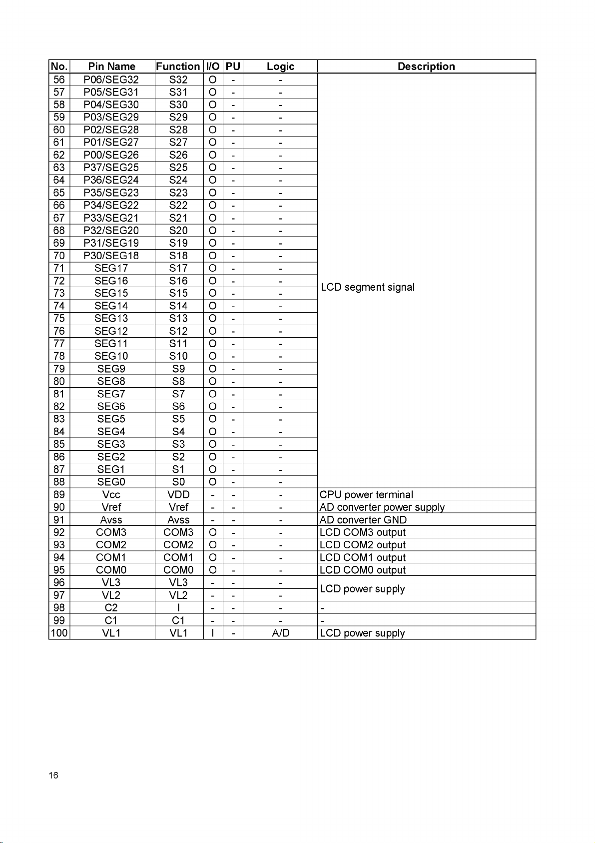
Pin Name Function I/O PU Logic Description
P06/SEG32 S32 O
P05/SEG31 S31 O
- -
- -
P04/SEG30 S30 O - -
P03/SEG29 S29 O - -
P02/SEG28 S28 O - -
P01/SEG27 S27 O
P00/SEG26 S26 O
P37/SEG25 S25 O
- -
- -
- -
P36/SEG24 S24 O - -
P35/SEG23 S23 O
- -
P34/SEG22 S22 O - -
P33/SEG21 S21 O
P32/SEG20 S20 O
P31/SEG19 S19 O
P30/SEG18 S18 O
SEG17 S17 O
SEG16 S16 O
SEG15 S15 O
SEG14 S14 O
SEG13 S13 O
SEG12 S12 O
SEG11 S11 O
SEG10 S10 O
SEG9 S9 O
SEG8 S8 O
SEG7 S7 O
SEG6 S6 O
SEG5 S5 O
SEG4 S4 O
SEG3 S3 O
SEG2 S2 O
SEG1 S1 O
SEG0 S0 O
Vcc VDD
Vref Vref
Avss Avss
COM3 COM3 O
COM2 COM2 O
COM1 COM1 O
COM0 COM0 O
VL3 VL3
VL2 VL2
C2 I
C1 C1
VL1 VL1 I
- -
- -
- -
- -
- -
- -
- -
- -
- -
- -
- -
- -
- -
- -
- -
- -
- -
- -
- -
- -
- -
- -
- - -
- - -
- - -
- -
- -
- -
- -
- - -
- - -
- - - -
- - - -
-
A/D LCD power supply
LCD segment signal
CPU power terminal
AD converter power supply
AD converter GND
LCD COM3 output
LCD COM2 output
LCD COM1 output
LCD COM0 output
LCD power supply
16
Page 18
SEMICONDUCTOR DATA
1) M5218FP (XA0068)
Dual Low Noise
Operational Amplifiers
Pin Assignment
8 Power Supply Plus
7 Output 2
6 Inverting Input 2
5 Non Inverting Input 2
o
3 2 1
3) TC4S66F (XA0115)
Bilateral Switch
1. OUTPUT
2. COMMON
3. INPUT
17
Page 19
4) TK10930VTL (XA0223)
Parameter Symbol Ratings Unit
Supply voltage Vcc max 10.0 V
Power dissipation Pd 400 mV
Storage temperature Tstg -55~+150
Operating temperature Top -30~+75
Operating voltage Vop 2.5~8.5 V
Operating frequency fop ~60 MHz
°C
°c
Parameter Symbol
Supply Current 1 lcc1 6.8 8.9 mA No signal, AM ON
Supply Current 2 lcc2 3.9 5.3 mA No signal, AM OFF
Mixer Coversion Gain Mg 20 dB
Mixer Input Impedance Mz 3.6
FM
Limiting Sensitivity Limit 2.0 8.0
Output Voltage Vo1 85 150 230 mVrms 10mVin +/-3kHz DEV
Distortion THD1 1.0 2.0 % 10mVin +/-3kHz DEV
Output Impedance Zo 800
Filter Gain Gf 30 38 dB Fin=30kHz, Vo=100mV
Scan Control Hi Voltage SH 2.3 V Squelch input=2.5V
Scan Control Low Voltage SL 0.3 V Squelch input=0V
Squelch Hysteresis Hys 30 mV
S meter Output Voltage S0 0.05 0.5 V Vin=0mV, RS=68kn
S meter Output Voltage S1 0.05 0.5 0.9 V Vin=0.01mV, RS=68kn
S meter Output Voltage S2 0.7 1.2 1.7 V Vin=0.1mV, RS=68kfi
S meter Output Voltage S3 1.2 1.8 2.5 V Vin=1mV, RS=68kO
S meter Output Voltage S4 1.6 2.3 2.9 V Vin=10mV, RS=68kQ
S meter Output Voltage S5 1.8 2.4 2.9 V Vin=100mV, RS=68kQ
AM
Sensitivity US 20 15
Output Voltage Vo2 60 120 160 mVrms 1kHz, 30%, Vin=1mV
Distortion-1 THD2 1.0 2.0 % 1kHz, 30%, Vin=1mV
Distortion-2 THD3 2.0 4.0 % 1kHz, 30%, Vin=1mV
S/N S/N 40 48 dB 1kHz, 30%, Vin=1mV
AM OFF Vo -0.3 0.3 %
Ratings
Min Typical Max
Unit Condition
DC Test
Kn
-3.0dB
HV
n 10mVin
required input level to get
H-V
20mV rms output
18
Page 20
5) BU4052BF (XA0236)
Analog Multiplexer/Demultiplexer
6) TC4W53FU (XA0348)
Multiplexer/Demultiplexer
Function Table
Control input
INH
L
L H
H
* Don’t Care
A
L
*
ON channel
ch0
ch1
NONE
COMMON 1
INH
VEE
VSS
8 VDD
2
3
4
4^
cn
co
7 ch0
6 ch1
5 A
19
Page 21
7) M64076GP (XA0352)
Dual PLL Synthesizer
XBo
SI
CPS
RST
Vcc
Fini
_ock1
Pd1
VT1
VF
1
□
2 19
□
3 18
□
4
□
5
□
6
□
7
□
8 13
□
9 12
□
10
□
Equivalent Circuit
F¡n2(Í5)
--------
SW
3
o>
4*
o
>1
O)
a
"O
Ja M P~>
SW
20
□
□
□
17
□
16
□
15
□
14
□
□
□
11
□
GND
Xin
Xout
OP2
OP1
Fin2
Lock2
PD2
VT2
GND
1/64, 65
2 modules
prescaler
Parameter Symbol Condition Min. Typ. Max. Unit
Power supply voltage Vcc
LPF supply voltage VF
Local oscillator input level Vin
Local oscillator input frequency Fin
Xin input level Vxin
Xin input frequency Fxin
Fin=80~520MHz
Vin=-10dBm
Fin=80~520MHz
Vin=-20~-4dBm
Vcc=2.7~5.5V
Vcc=2.7~5.5V
Fxin=10~25MHz
Sine wave
Vcc=2.7~5.5V
Vxin=0.4~1.4Vp-p
2.7 5.5 V
-20 -4 dBm
80 520 MHz
0.4 1.4
10 25 MHz
Data latch (17bit)
Local 2
programmable divider
Data latch (16bit)
9 12 V
Vp-p
0
XBo
Xout(18¡
X in ^ )-
Fin 1(6
s i © -
I
CPS(3>-
-----
<ÄMP
i— [am ^ >
SW
OSC
SW
1/64, 65
2 modulus
prescaler
21 bit shift resistor
21 bit pulse counter
1/2
divider
-0 -
RST
Reference frequency 2
programmable divider
Reference frequency 1
programmable divider
Data latch (16bit)
Local 1
programmable divider
Data latch (17bit) —
Data latch (6bit)
Latch
selector
GND
BU£>
------
(ij)GND
(Í7)O P2
20
Page 22
8) LA4425A (XA0410)
5W Audio Power Amplifiers
9) M67746 (XA0412)
144 ~ 148MHz 60W
RF Power Module
1 2 3 4 5
Rating Symbol Ratings Unit
Supply voltage Vcc 17 V
D
Fin(Ground)
(U
E ^
r e
3 o
c co
M67746
1 2 3 4
>
O lo
in
o
Q <N
(D ^
5? ^
£0 C
to^ 'F
3 <N
(A t-
Q £
g 1
¡7 a
o
Id
3 C
# 1=
o .2
c
G
Total current Icc 20 A
Input power Pin(max) 600 mW
Output Power Po(max) 70 W
Operation case temperature Tc(op) -30 to + 110 °C
Strage temperature
Zg=Zl=50fi
Tstg
-40 to + 110 °c
21
Page 23
10) M68729 (XA0591)
220 ~ 246MHz 30W
RF Power Module ABSOLUTE MAXIMUM RATING(TC = 25°C)
Rating Symbol Ratings Unit
Supply voltage Vcc 17 V
Total current Icc 10 A
Fin(Ground)
Input power Pin(max) 600 mW
Output Power Po(max) 40 W
Operation case temperature Tc(op) -30 to + 110 °C
Strage temperature Tstg -40 to + 110
ELECTRICAL CHARACTERISTICS
°c
PIN :
® Pin RF INPUT
© Vcc1 1st. DC SUPPLY
® VCC2 2nd. DC SUPPLY
© PO
© GND
: RF OUTPUT
: FIN
Symbol
Po
%
2fo
3fo
pin
Parameter
f Frequency range
Output power
Total efficiency
2nd. harmonic
3rd. harmonic
Input VSWR
Load VSWR tolerance
-
Test conditions
Vcc1,2 = 12.5V
Pin - 300mV
Zg = Zl = 50fi
VCC1,2 = 15.2V
Po = 30W(Pin = Controlled)
Load VSWR = 20:1 (All phase),
Zg = 500
Limits
Min Max
220 246 MHz
30 W
40 %
No degradation
or destroy
Unit
-30 dBc
-30 dBc
3
-
-
22
Page 24

11) M57788M (XA0077)
OUTLINE DRAWING Dimensions in mm
BLOCK DIAGRAM
GHH -
PIN :
©Pin : RF INPUT
®VCC1 : 1st. DC SUPPLY
®VCC2 : 2nd. DC SUPPLY
©VCC3 : 3rd- DC SUPPLY
®PO : RF OUTPUT
®GND : FIN
ABSOLUTE MAXIMUM RATINGS ( T c = 2 5 " C u n le s s o t h e r w i s e n o t e d )
S y m b o l
V c c i
V CCZ , 3
c c
PinOr tax)
P O (m ax)
T cC O P)
T st g
P a r a m e t e r
S u p p l y v o l t a g e
T o t a l c u r r e n t
I n p u t p o w e r
O u t p u t p o w e r
O p e r a t i o n c a s e t e m p e r a t u r e
S t o r a g e t e m p e r a t u r e
Z g = Z l = 5 0 0
Z g = Z u = 5 0 Q
C o n d i tio n s
.ELECTRICAL CHARACTERISTICS f T c - 2 5 V u n l e s s o t h e r w i s e n o t e d )
S y m b o l
f F r e q u e n c y r a n g e
P o
77 T
2 f o
p in
O u t p u t p o w e r
T o t a l e f f ic ie n c y
2 n d . h a r m o n i c
I n p u t V S W R
L o a d V S W R t o le r a n c e
-
P a r a m e t e r
P in = 0 . 4 W
V c c = 1 2 . 5 V
Z g = Z l = 5 0 S i
V c c = 1 5 . 2 V ,
P o = 4 0 W ( P in : c o n t r o l le d )
L o a d V SWR= 8 .8 : 1 ( A l 1 p h a s e ) . 2 s e c .
Z g = 5 0 O
T e s t c o n d i ti o n s
R a t in g s
1 6
1 7
1 2
0 . 5
5 0
- 3 0 - 1 1 0 V
- 4 0 - 1 1 0 X
L i m i ts
M i n M a x
4 3 0
4 0
4 0
- 3 0 d B
N o d e g r a d a t io n
4 5 0
2 . 8
U n it
V
V
A
W
W
U n i t
M H z
W
%
-
-
23
Page 25

12) |iPC2710T (XA0449)
RF Amplifier
Parameter Symbol Condition Ratings Unit
Supply voltage Vcc 5.0 V
Circuit current Icc Vcc=5V, no signa 22 mA
Power gain GP Vcc=5V, f=500MHz 33 dB
Staturated output power Po(sat) Vcc=5V, f=500MHz, Pin=-8dBm +13.5 dBm
Noise figure NF Vcc=5V, f=500MHz 3.5 dB
Upper frequency (-3dB) fu Vcc=5V, Reference freq. =100MHz 1000 MHz
Isolation ISL Vcc=5V, f=500MHz 39 dB
Input return loss RL in Vcc=5V, f=500MHz 6 dB
Output return loss RL out Vcc=5V, f=500MHz 12 dB
Gain flatness
Test Circuit
Gp
Vcc
Vcc=5V, f=0.1~0.6GHz 0.8 dB
Top View
13) NJM2902 (XA0596)
Pin Assignment
(Top View)
1. A OUTPUT
2. A-INPUT
3. A+INPUT
4. V+
5. B+INPUT
6. B-INPUT
7. B OUTPUT
8. C OUTPUT
9. C-INPUT
10. C+INPUT
11. GND
12. D+INPUT
13. D-INPUT
14. D OUTPUT
GND
GND 2
Input
3
4 Output
LL
5 GND
C)
1
6 Vcc
24
Page 26

14) 24LC32A (XA0604)
PDIP
A 0 l=
A 1 I=
A 2 I=
Vssl=
V J
1
N>
4^
2
1“
o
w
3
N>
>
4 b
=□ Vcc
8
7
=□ WP
fi
=□ SCL
=□ SDA
15) S-80845ALMP-EA9-T2 (XA0620)
Name
A0..A2
Vss
SDA
SCL
WP Write Protect Input
Vcc
User Configurable Chip Selects
Ground
Serial Address/Data I/O
Serial Clock
+2.5V-6.0V Power Supply
Function
GND Vin Vout
16) L88MS05TLL (XA0675)
5 V V o ltag e R eg u la to r W ith O n /O ff Fu n ction
Pin Assignment
1. VIN
o
1 2 3 4 5
2. STB
3. GND
4. Cn
5. VOUT
25
Page 27

17) AN8010M (XA0119)
V o ltag e R e g u lato r
Test Circuit
<
o
u u u
Output Common Input
AN8010M
18) TK10489M (XA0314)
26
Page 28

19) Transistor, Diode, and LED Outline Drawings
Top View
RLS-73
xD0363
1SS355
xD0254
1SS356
'X"D0"272"'
1SV214
'XDÔÎ3Î'
1SV237
'X'D trnf
1SV262
xD0300
1SV268
xD0301
O
DA204U
"X"DÖi3Ö"
n
'S — B -
K
MI407
"XD00"Ï3"'
2SB1132
xT0061
C
2SC4215
xT0124
C
_ B _
QY
"B—S'
B É
DTC144YU
xU0029
C
64
"B—B-
B É
XP1215
' xU0"i78"
B2 é B1
B B B.
9M
a
DAN235U
xD0246
"s—S'
M
2SK508
"XÉ00Ï0"
G
_B_
K52
~B—B-
S D
2SB1292F
xT0112
0
B1292
BCÉ
2SC4226
xT0141
C
_B_
R24
"B—B-
B é
FA1111C
xL0069
_ _
1 r
in i
*
DSA3A1
"xDöiäi"
2SK880GR
xÉ0021
G
_B_
XG V12 FR
■B — B -
S D
2SC2954
XTÖ084
C C
Is 1
u u u
2SC4245
..XT0Ä2K..
C
HB 26
"B—B-
B é
.FAÏ.Ï1TC.
xL0077
__
[□]
----
1
MA304
x'DÖ299"
3SK131<12
'"'XÉ0028'"'
G1 G2
_B__B_
B B
D S
2SC3356
'"XTÖ03Ö"'
n
R24
R r
.3SK184S..
„X É 00ÏL
3RS
UDZ5.1B
""XD 0165"
I bb|
MA729
xD0300
2SA1036K
xT0110
C
_ B _
HQ
'S—B-
B É
2SC3357
xT0048
C
n
LU
R R
DTA114YU
xU0112
C
_B_
54 24
"B—B-
B é
UMC3TR
xU0047
É2 B1 É1
B 1=1 R
V12 C5
"B
---
B
C2 C1/B2
f t
MA8100
xD0297
2SA1576
xT0094
C
_ B _
2SC4081
XT0Ö95
C
B
BR JP
DTC114EU
xU0131
C
B—B-
B é
UMC5N
"xU"0T52"
É2 B1 É1
1=1 B H .
“Ö
C1/B2
MA742
xD0250
■Q—S'
M1U
2SA1736
xT0099
LD
U U U
B C É
2SC4099
xT0096
C
1=1
..DICT44EUA.
xU0148
C
_b _
"B—B-
B É
U1BC44
XD0Ï35 "
27
Page 29

20) LCD Connection (TTR3626UPFDHN)
28
Page 30

EXPLODED VIEW
1) Top and Front View
AA0050
DR-135
DR-235
DR-435
NK0072
»T. E. TA
KZ0105
»TG. EG. TAG
KZ0120
29
Page 31

2) Bottom View
AA0050
30
Page 32

3) LCD Assembly
FF0017
CPU BOARD
31
Page 33

:o ;o ;o ;o ;o; o; o; o; oO O O OO O OOO O O OO
3J3J3J3J3J3J3J3J3JXX
wwwwwwwwwoo
o o o o o o o o o - * - - * -
W W M M Ü l O iW O O l- » -!
W C O W W O O ^ - 'J i M W
oooooooooooooooooooooo
S'?????????????????????
T3 T3' T3' ~o' ~o' ~0~ ~0~ ~0~ ~0~ ~0~ ~0~ ~0~ ~0~ ~0~ ~0~ ~0~ ~0~ ~0~ ~0~ ~0~ ~0~ ~0~
po popopo pop opopopoHH-IH HH-l-I HH- IHH
O O O O O O '
^ ^ ^ ^ ^ ^
0 o o o o o '
co co
CO CO CO CO CO CO '
m m
m m m m m m i
N N
N N N N N N I
1 I I I I I :
oi oi ->•—>• ho o I
O) O) o o ho o i .
o o co co co o co
sU sU sU sU sU sU sU sU sU sU sU sU sU sU sU sU sU sU sU sU sU sU sU sU sU sU sU sU sU sU sU sU sU sU sU sU sU sU sU sU sU sU sU sU sU sU sU sU sU sU sU sU sU sU sU sU sU sU sU sU sU sU sU sU sU sU sU sU sU sU sU sU sU sU sU sU sU sU sU sU sU
CD CD CD CD CD CD <D<D<D<D<D<D<D<D<D<D
C 23 23 73 73 73 ^3 ^3 ^3 ^3 ^3 ^3 ^3 ^3 ^3 ^3 ^3 ^3 ^ 3 ^3 ^3 ^3 ^3 ^3 ^3 ^3 ^3 ^3 ^3 ^3 ^3 ^3 ^3 ^3 ^3 ^3 ^3 ^3 ^3 ^3 ^3 ^3 ^ 3 ^ 3 ^3 ^3 ^3 ^3 ^3 ^3 ^3 ^3 ^3 ^3 ^3 ^3 ^3 ^3 ^3 ^3 ^3 ^3 ^ 3 ^ 3 ^3 ^3 ^3 ^3 ^3 ^3 ^3 ^3 ^3 ^3 ^3 ^3 ^3 ^3 ^3 ^3
oco^cocococococococ ocoococococococococo cocococococococococ ococococococococococ ococococococococococ ococococococococococ ococococococococococ ocococococococococo
OOO OOO O OOO OOO OOO OOO OOO OOO OOO OOO OOO OOO OOO OOO OOO OOO OOO OOO OO O OO O OO O OO OOO OOO OOO OOO Or~
-iai-iO)CouiwwaiaiaijiOcowcocoK)cojiMcoai'JO)jiaiM aiMAhoui'Jcotocoo)ai-NiaiO)CocoNicococoaihoaiwi\)0)aiaijiO)UijiCoiicocococoaia iaiaiO)cocojiO)00^o.
ÜlO-t^hOhOOCOCOO-t^OO)COCOOCOCOCOhOO)0)hOOhOhOO)00)00)0)0)0-t^-t^O)-t^O)0-t^OhOCOCOOCOCOCOOO)000)hOCOOCDhOhO~-J-t^-t^COCOCOCOOOOO-t^COOO)hO->-->-CO-»-'
73 D O OOO O OOO OOOO OOO O OOO O OOO O OOO O OOO O OOO OOO OOO O OOO OOO O OO O OOO OOO O OOO OOO OOO O OOO OOO O OOO
3333333333333
3333333333333
œœœœœœœœœœœœœ
cri cri ui tri tri tri cri co' œ' œ' œ' œ' c/)'
o o o ’ S 'S' S'ooS'S' oS'S'
D D D D
H H H H
> > > O
-fc* -fc* -fc* -t*
-< -< -< m
c c c c
> > > >
H H H H
X X X X X X
c c H H C C
o o o o
- - o o
° ° ffi
003
■t* -t* :
m -< 1
c c
> > ;
H H ■
O) CO CO CO
CO h H W
2 2 2^
o ^ i o
CO ^ Ji CO
-*• m m 2
H c c *
S > > J
O) —I —I -t*
— O)
x x x m s c
H C C [- > c_
5 9 S R O o
o O
K5 i_<
CO 10
CD-I;
—I —I I i
o o jo ■
m -< 05 .
c c c
> > T) 1
H d :
: D :
XXX
> > >
^ o o o
0 0)0)0)
^ si W O
-J OI O -t*
CO -fc>
O OI
3 >
S S S S S S S S S § § § S 2 S m 2 Q Q Q 0 0 0 m m m m m m m m m m 2 Q Q Q Q Q Q Q Q Q S 8 Q S 8 2 0 m 2
XXX
X X X X
> D D
D D D D '
O O o
O O O O '
CO CO ho
ID O lff iO O l^W l DÜ i;
-»• O) CO
03 CO -i
OOO OO OOOOO OOOOO OO O
--------------------------
C -o' T3' ~o' ~o' ~o' ~o' ~o' ~o' ~o' ~ o' ~o' ~o' ~o' ~o' ~o ' ~o'
o' o' o' o' o' o' o' H o' o' o' !
Q.Q.Q.Q .Q.Q.Q.OQ .Q.Q.1
S c s c '
> D > D 1
-J N -J N I
X X
XXX X X XXC
D D
o o
-------------------------------------------
^> C0 >> >>>>!
r71of:H_|Oooooo;
h m ’
o O O O
O O O O
-J -vl O) OJ
-J -J CO oi
7] 7]
o o
C C 0 0 0 0 0 0 0 0 0 0 0 0 0 0 0 0 0 0 0 0 0 0 0 0 0 0 0 0 0 '
mmc cco co coccc cc cc ccccocc cc occcccccc c'
OOCOCOOOOWWCOCOCOCOCOCOCOWOCOCOCOOCOCOCOCOCOCOCOCOCO'
C O CO O O O J O C O O O O O OO O —“■—“- O O J O O O O —i - O O —“- 0 0 0 —“-O
IDCDAANlJiCDCOCOCOCOAW^O-iCONlCO-i-i^O-ti-ti-iArOW-iJi.
COCO~-J~-JhOCDJ^01010101~-J01~-J-»--»-01h001J^J^CD-»-COCO->-COCOCO->-CDl
.. _oooooooooooooooooooooooooooooooooo
? Ô' 2 o ????????????????????????????????
~o' ~o' ~o' ~o' ~o' ~o' ~o' ~o' ~o' ~o' ~o' ~o' ~o' ~o' ~o' ~o' ~o' ~o' ~o' ~o' ~o' ~o' ~o' ~o' ~o' ~o' ~o' ~o' ~o' ~o' ~o' ~o'
. O
PPSTSTST QOOOQOQQQOSr OOO ST 0 0 0 0 0 0 0 0 0 0 0 0
H H O
£ £ 2 2 i
g g § § g
CO 03 03 CO £
o o x I
! ! s s i
ÏÏ ïï ^ ^ |
8 §
o o o o o o o o o h o o o h o o o o o o o o o o o o
O) O)
O) O)
o o g
CO s co
5 CD m
o 2 2
^ -fc. I
O ~-J —»•
010)0
0 o
CO CO
CD CD
1 I
O o
0 o
CO CO
CD CD
1 I
O o
O) O)
0 o
CO CO
CD CD
1 I
O o
CO CO CO :
O) O) 1
O O '
CO CO '
in Q :
CO CO CO CO CO
CD CD CD CD CD
O ï ï O ï
-fc> -fc> -fc> ->■ -fc>
"J -vl -v l o ~- J
0)0)0)0 0)0)0)
o o o o o o o
CO CO CO CO CO CO CO
5 5 CD CD CD CD CD
^ ^ O m m o o
O CD <D 1
o
■0
C
PARTS LIST
o o o o
^ ^ ^ ^
0 o o o
co co co co
m m m m
N N N N
1 I I I
CO
co co
m m
N N
CO CO CO CO CO CO I
O O
73 73
o o
co co
m m
N N
ï ï
o ;
O O
O O O O
73 73
^ ^ ^ ^
O o
0 o o o
co co
S °
[n m
;< N
co co co co
m m m m
m m
N N
N N N N
ï ï
1 I I I
O O O O ' O CO OC OO ~v lOO OO ~-J O'
0 o o o o
co co co co co
m m m m m
N N N N N
1 I I I I
-i.-i.COJ^J^hOCO-».CO-».hO-».'
O O O O
^ ^ ^ ^
0 o o o
co co co co
m m m m
N N N N
1 I I I
O O O
^ ^ ^
o o o
co co co
m m m
N N N
I I I
O O O O
^ ^ ^ ^
0 o o o
co co co co
m m m m
N N N N
1 I I I
O O O
O O O O
^ ^ ^
^ ^ ^ ^
o o o
0 o o o
co co co
co co co co
m m m
m m m m
N N N
N N N N
I I I
1 I I I
hOOOOOOO-JOOOOOOOO
■tiCOOlCOAtOMAtOtOtOCO-iCOCO-i
O O O O
^ ^ ^ ^
0 o o o
co co co co
m m m m
N N N N
1 I I I
O O O O
^ ^ ^ ^
0 o o o
co co co co
m m m m
N N N N
1 I I I
O O O O O
73 73 73 73 ?D
0 O O O O
co co co co co
m m m m m
N N N N N
1 I I I I
o o o
^ ^ ^
o o o
co co co
m m m
N N N
III
CO
o o o o o
73 73 73 73 ^3
0 o o o o
co co co co co
m m m m m
N N N N N
1 I I I I
Ü1 co
O) -J CO o o o
O O O O O
73 73 73 73 ?D
0 O O O O
co co co co co
m m m m m
N N N N N
1 I I I I
O O O O O O
73 73 73 73 ^3 ^3
0 O O O O O
co co co co co co
m m m m m m
N N N N N N
1 I I I I I
-j o o o
t-O -fc* o o
O O O O O
73 73 73 73 ^3
0 O O O O
co co co co co
m m m m m
N N N N N
1 I I I —
0 0 0 )0
Page 34

Ref.
Parts No. Description Parts Name
No. DR-135 DR-235 DR-435
SW1 UU0015Z Switch EVQPPXA25 1 1 1
SW2 UU0015Z Switch EVQPPXA25 1 1 1
SW3 UU0015Z Switch EVQPPXA25 1 1 1
SW4 UU0015Z Switch EVQPPXA25 1 1 1
SW5 UU0015Z Switch EVQPPXA25 1 1 1
SW6 UU0015Z Switch EVQPPXA25 1 1 1
SW7 UU0015Z Switch EVQPPXA25 1 1 1
VR1 RV0035 Variable EVUF2JFK4B14 1 1 1
W1 UX1270 Wire WIRE DR235 W1 1 1 1
X1 XQ0131
TL0024
YZ0042
ST0068
FG0305
TL0023
DG0037
FM0034
FP0034
ST0064
Xtal CSA310/3.6864MHZ
DIFFUSION SHEET 135
CEMENT G17 / 1G
DIAL FITTING
LCD RUB.CONNECT. 135
REFLECTION DR135
LCD LIGHT DR135
MIC GND PLATE
MIC SPACER DR110
LCD HOLDER DR135
Qty
1
1
1
1
1
1
1
1
1
1
1
1
1
1
1
1
1
1
1
1
Main Unit (DR-135)
Ref.
Parts No. Description Parts Name
No.
C101 CU3047 Chip C. C1608JB1H103KT-N 1
C102 CU3047 Chip C. C1608JB1H103KT-N 1
C103 CS0049 Chip tantalum TMCSA1C105MTR 1
C104 CU3047 Chip C. C1608JB1H103KT-N 1
C105 CS0394 Chip tantalum TMCMB0J476MTR 1
C106 CU3051 Chip C. C1608JB1E223KT-NS 1
C107 CU3111 Chip C. C1608JB1C104KT-N 1
C108 CU3047 Chip C. C1608JB1H103KT-N 1
C109 CS0216 Chip tantalum TMCMB1A106MTR 1
C110 CU3047 Chip C. C1608JB1H103KT-N 1
C111 CU3047 Chip C. C1608JB1H103KT-N 1
C112 CU3047 Chip C. C1608JB1H103KT-N 1
C113 CU3047 Chip C. C1608JB1H103KT-N 1
C114 CU3047 Chip C. C1608JB1H103KT-N 1
C115 CU3047 Chip C. C1608JB1H103KT-N 1
C116 CU3047 Chip C. C1608JB1H103KT-N 1
C117 CU3047 Chip C. C1608JB1H103KT-N 1
C118 CU3049 Chip C. C1608JB1E153KT-NS 1
C119 CU3051 Chip C. C1608JB1E223KT-NS 1
C120 CU3021 Chip C. C1608CH1H680JT-AS 1
C121 CU3005 Chip C. C1608CH1H040CT-AS 1
C122 CU3002 Chip C. C1608CH1H010CT-AS 1
C123 CU3015 Chip C. C1608CH1H220JT-AS 1
C124 CU3040 Chip C. C1608JB1H272KT-NS 1
C125 CU3044 Chip C. C1608JB1H562KT-NS 1
C126 CU3038 Chip C. C1608JB1H182KT-AS 1
C127 CU3041 Chip C. C1608JB1H332KT-NS 1
CU3111 Chip C. C1608JB1C104KT-N 1
C129
C130 CS0049 Chip tantalum TMCSA1C105MTR 1
CU3035 Chip C. C1608JB1H102KT-AS 1
C132
C133 CU3005 Chip C. C1608CH1H040CT-AS 1
CU3042 Chip C. C1608JB1H392KT-NS 1
C134
C135 CU3044 Chip C. C1608JB1H562KT-NS 1
CU3017 Chip C. C1608CH1H330JT-AS 1
C137
C138 CS0049 Chip tantalum TMCSA1C105MTR 1
CU3017 Chip C. C1608CH1H330JT-AS 1
C139
C140 CU3017 Chip C. C1608CH1H330JT-AS 1
CU3111 Chip C. C1608JB1C104KT-N 1
C141
C142 CU3111 Chip C. C1608JB1C104KT-N 1
CU3111 Chip C. C1608JB1C104KT-N 1
C143
C144 CU3047 Chip C. C1608JB1H103KT-N 1
C145 CU3003 Chip C. C1608CH1H020CT-AS 1
C146 CE0339 Electrolytic C. 16MV 10SWB+TS 1
C148 CU3017 Chip C. C1608CH1H330JT-AS 1
C149 CU3017 Chip C. C1608CH1H330JT-AS 1
C150 CU3005 Chip C. C1608CH1H040CT-AS 1
C151 CU3047 Chip C. C1608JB1H103KT-N 1
C152 CE0339 Electrolytic C. 16MV 10SWB+TS 1
C153 CU3035 Chip C. C1608JB1H102KT-AS 1
C154 CU3035 Chip C. C1608JB1H102KT-AS 1
C155 CU3007 Chip C. C1608CH1H060CT-A 1
C156 CU3047 Chip C. C1608JB1H103KT-N 1
C157 CU3035 Chip C. C1608JB1H102KT-AS 1
C158 CU3013 Chip C. C1608CH1H150JT-AS 1
C159 CU3035 Chip C. C1608JB1H102KT-AS 1
C160 CE0339 Electrolytic C. 16MV 10SWB+TS 1
C161 CU3111 Chip C. C1608JB1C104KT-N 1
C162 CU3035 Chip C. C1608JB1H102KT-AS 1
C165 CU3111 Chip C. C1608JB1C104KT-N 1
C167 CU3047 Chip C. C1608JB1H103KT-N 1
C168 CU3111 Chip C. C1608JB1C104KT-N 1
C169 CU3027 Chip C. C1608CH1H221JT-AS 1
C171 CU3111 Chip C. C1608JB1C104KT-N 1
C172 CU3035 Chip C. C1608JB1H102KT-AS 1
Qty
DR-135DR-235 DR-435
Ref.
Ver
1
1
1
1
1
1
1
1
1
1
Ver
Parts No. Description Parts Name
No.
CU3037 Chip C. C1608JB1H152KT-AS 1
C173
C174 CU3029 Chip C. C1608JB1H331KT-AS 1
CU3111 Chip C. C1608JB1C104KT-N 1
C175
C176 CU3018 Chip C. C1608CH1H390JT-AS 1
CU3018 Chip C. C1608CH1H390JT-AS 1
C177
C179 CU3111 Chip C. C1608JB1C104KT-N 1
CU3035 Chip C. C1608JB1H102KT-AS 1
C180
C181 CU3035 Chip C. C1608JB1H102KT-AS 1
CU3047 Chip C. C1608JB1H103KT-N 1
C182
C183 CU3035 Chip C. C1608JB1H102KT-AS 1
CU3035 Chip C. C1608JB1H102KT-AS 1
C184
C185 CS0232 Chip tantalum TMCMA1V474MTR 1
CU3008 Chip C. C1608CH1H070CT-A 1
C186
C187 CU3035 Chip C. C1608JB1H102KT-AS 1
C188 CU3035 Chip C. C1608JB1H102KT-AS 1
C189 CU3011 Chip C. C1608CH1H100DT-AS 1
C190 CU3047 Chip C. C1608JB1H103KT-N 1
C191 CU3102 Chip C. C1608JB1C333KT-NS 1
C192 CU3047 Chip C. C1608JB1H103KT-N 1
C193 CU4033 Chip C. GRM42-6X7R102K500PT 1
C194 CU3012 Chip C. C1608CH1H120JT-AS 1
C195 CU3012 Chip C. C1608CH1H120JT-AS 1
C196 CU3023 Chip C. C1608CH1H101JT-AS 1
C197 CU4003 Chip C. GRM42-6CK020C500PT 1
C198 CE0339 Electrolytic C. 16MV 10SWB+TS 1
C199 CE0339 Electrolytic C. 16MV 10SWB+TS 1
C200 CU3035 Chip C. C1608JB1H102KT-AS 1
C201 CU4014 Chip C. GRM42-6CH180J500PT 1
C202 CU4016 Chip C. GRM42-6CH270J500PT 1
C203 CU4016 Chip C. GRM42-6CH270J500PT 1
C204 CU4013 Chip C. GRM42-6CH150J500PT 1
C205 CU3035 Chip C. C1608JB1H102KT-AS 1
C206 CE0339 Electrolytic C. 16MV 10SWB+TS 1
C207 CU3002 Chip C. C1608CH1H010CT-AS 1
C208 CU3002 Chip C. C1608CH1H010CT-AS 1
C209 CU3035 Chip C. C1608JB1H102KT-AS 1
C210 CU3003 Chip C. C1608CH1H020CT-AS 1
C211 CU3003 Chip C. C1608CH1H020CT-AS 1
C212 CE0364 Electrolytic C. 16MV 47SWB+TS 1
C213 CU3035 Chip C. C1608JB1H102KT-AS 1
C214 CU3015 Chip C. C1608CH1H220JT-AS 1
C215 CU4016 Chip C. GRM42-6CH270J500PT 1
C216 CU4016 Chip C. GRM42-6CH270J500PT 1
C217 CU3051 Chip C. C1608JB1E223KT-NS 1
C218 CU3051 Chip C. C1608JB1E223KT-NS 1
C219 CU3035 Chip C. C1608JB1H102KT-AS 1
C220 CU3035 Chip C. C1608JB1H102KT-AS 1
C221 CU3047 Chip C. C1608JB1H103KT-N 1
C222 CU3035 Chip C. C1608JB1H102KT-AS 1
C223 CE0364 Electrolytic C. 16MV 47SWB+TS 1
C224 CU3023 Chip C. C1608CH1H101JT-AS 1
C225 CU3035 Chip C. C1608JB1H102KT-AS 1
C226 CU3035 Chip C. C1608JB1H102KT-AS 1
C227 CS0049 Chip tantalum TMCSA1C105MTR 1
C228 CU3035 Chip C. C1608JB1H102KT-AS 1
C229 CU3101 Chip C. C1608JB1C473KT-NS 1
C230 CU3035 Chip C. C1608JB1H102KT-AS 1
C231 CU3035 Chip C. C1608JB1H102KT-AS 1
C232 CU3035 Chip C. C1608JB1H102KT-AS 1
C233 CU3035 Chip C. C1608JB1H102KT-AS 1
C234 CU3035 Chip C. C1608JB1H102KT-AS 1
C235 CU3014 Chip C. C1608CH1H180JT-AS 1
C236 CU3014 Chip C. C1608CH1H180JT-AS 1
C237 CU3035 Chip C. C1608JB1H102KT-AS 1
C238 CS0049 Chip tantalum TMCSA1C105MTR 1
C239 CS0049 Chip tantalum TMCSA1C105MTR 1
C240 CE0339 Electrolytic C. 16MV 10SWB+TS 1
CU3022 Chip C. C1608CH1H820JT-AS 1
C241
C242 CU3051 Chip C. C1608JB1E223KT-NS 1
CE0339 Electrolytic C. 16MV 10SWB+TS 1
C243
C244 CE0339 Electrolytic C. 16MV 10SWB+TS 1
CS0049 Chip tantalum TMCSA1C105MTR 1
C245
C246 CU3043 Chip C. C1608JB1H472KT-NS 1
CU3111 Chip C. C1608JB1C104KT-N 1
C247
C248 CU3047 Chip C. C1608JB1H103KT-N 1
CU3038 Chip C. C1608JB1H182KT-AS 1
C249
C250 CU3026 Chip C. C1608CH1H181JT-AS 1
CE0339 Electrolytic C. 16MV 10SWB+TS 1
C251
C252 CU3035 Chip C. C1608JB1H102KT-AS 1
CU3111 Chip C. C1608JB1C104KT-N 1
C253
C254 CU3111 Chip C. C1608JB1C104KT-N 1
C255 CE0364 Electrolytic C. 16MV 47SWB+TS 1
C256 CU3111 Chip C. C1608JB1C104KT-N 1
C257 CE0339 Electrolytic C. 16MV 10SWB+TS 1
C258 CS0049 Chip tantalum TMCSA1C105MTR 1
C259 CU3035 Chip C. C1608JB1H102KT-AS 1
C260 CE0339 Electrolytic C. 16MV 10SWB+TS 1
C261 CU3035 Chip C. C1608JB1H102KT-AS 1
C262 CU3035 Chip C. C1608JB1H102KT-AS 1
Qty
DR-135 DR-235 DR-435
Ver
33
Page 35

Ref.
Parts No. Description Parts Name
No.
C263 CE0100 Electrolytic C. 16MV 22UW 1
C264 CU3031 Chip C. C1608JB1H471KT-AS 1
C265 CU3035 Chip C. C1608JB1H102KT-AS 1
C266 CU3064 Chip C. C1608CH1H1R5CT-AS 1
C267 CU3035 Chip C. C1608JB1H102KT-AS 1
C268 CU3035 Chip C. C1608JB1H102KT-AS 1
C269 CU3035 Chip C. C1608JB1H102KT-AS 1
C270 CU3047 Chip C. C1608JB1H103KT-N 1
C271 CU3035 Chip C. C1608JB1H102KT-AS 1
C272 CS0220 Chip tantalum TMCMA1C225MTR 1
C273 CS0220 Chip tantalum TMCMA1C225MTR 1
C274 CU3016 Chip C. C1608CH1H270JT-AS 1
C275 CU3047 Chip C. C1608JB1H103KT-N 1
C276 CE0339 Electrolytic C. 16MV 10SWB+TS 1
C277 CE0343 Electrolytic C. 16MV 1000HC+T 1
C278 CU3035 Chip C. C1608JB1H102KT-AS 1
C279 CU3051 Chip C. C1608JB1E223KT-NS 1
C280 CU3016 Chip C. C1608CH1H270JT-AS 1
CU3009 Chip C. C1608CH1H080CT-A 1
C281
C282 CU3064 Chip C. C1608CH1H1R5CT-AS 1
CU3027 Chip C. C1608CH1H221JT-AS 1
C283
C284 CU3002 Chip C. C1608CH1H010CT-AS 1
CU3035 Chip C. C1608JB1H102KT-AS 1
C285
C286 CU3027 Chip C. C1608CH1H221JT-AS 1
CS0063 Chip tantalum TMCSA1V104MTR 1
C287
C288 CU3011 Chip C. C1608CH1H100DT-AS 1
CU3051 Chip C. C1608JB1E223KT-NS 1
C289
C290 CU3035 Chip C. C1608JB1H102KT-AS 1
CU3011 Chip C. C1608CH1H100DT-AS 1
C291
C292 CU3035 Chip C. C1608JB1H102KT-AS 1
CU3035 Chip C. C1608JB1H102KT-AS 1
C293
C294 CU3035 Chip C. C1608JB1H102KT-AS 1
C295 CU3047 Chip C. C1608JB1H103KT-N 1
C296 CU3011 Chip C. C1608CH1H100DT-AS 1
C297 CU3035 Chip C. C1608JB1H102KT-AS 1
C298 CU3009 Chip C. C1608CH1H080CT-A 1
C299 CU3047 Chip C. C1608JB1H103KT-N 1
C300 CU3015 Chip C. C1608CH1H220JT-AS 1
C301 CU3023 Chip C. C1608CH1H101JT-AS 1
C302 CU3023 Chip C. C1608CH1H101JT-AS 1
C303 CU3023 Chip C. C1608CH1H101JT-AS 1
C304 CU3047 Chip C. C1608JB1H103KT-N 1
C305 CU3047 Chip C. C1608JB1H103KT-N 1
C306 CU3111 Chip C. C1608JB1C104KT-N 1
C307 CU3047 Chip C. C1608JB1H103KT-N 1
C308 CE0342 Electrolytic C. 16MV 470HC+TS 1
C309 CU3051 Chip C. C1608JB1E223KT-NS 1
C310 CU3023 Chip C. C1608CH1H101JT-AS 1
C311 CU3035 Chip C. C1608JB1H102KT-AS 1
C312 CU3011 Chip C. C1608CH1H100DT-AS 1
C313 CU3035 Chip C. C1608JB1H102KT-AS 1
C314 CS0237 Chip tantalum TMCMA1A475MTR 1
C315 CS0237 Chip tantalum TMCMA1A475MTR 1
C316 CS0237 Chip tantalum TMCMA1A475MTR 1
C317 CS0237 Chip tantalum TMCMA1A475MTR 1
C318 CU3035 Chip C. C1608JB1H102KT-AS 1
C319 CS0237 Chip tantalum TMCMA1A475MTR 1
C320 CS0237 Chip tantalum TMCMA1A475MTR 1
C321 CS0220 Chip tantalum TMCMA1C225MTR 1
C322 CU3035 Chip C. C1608JB1H102KT-AS 1
C323 CU3018 Chip C. C1608CH1H390JT-AS 1
C324 CU3016 Chip C. C1608CH1H270JT-AS 1
C325 CU3018 Chip C. C1608CH1H390JT-AS 1
C326 CU3029 Chip C. C1608JB1H331KT-AS 1
C327 CU3034 Chip C. C1608JB1H821KT-AS 1
CN101
UE0369 Connector AXN49301616 1
CN102
UE0397 Connector 10-5082-3110-17-100 1
CN103
UE0397 Connector 10-5082-3110-17-100 1
CN104 UA0037Y Wire DC CABLE UA0037 1
CN105
UE0394 Connector PI28A15M 1
CN106
UE0043 Connector PI22A02M 1
CN107
UE0393 Connector PI28A11M 1
CN110
UE0341 Connector PI28A02M 1
D101 XD0246 Chip Diode DAN235UT 106 1
D102 XD0299 Chip Diode MA304-TX 1
D103 XD0299 Chip Diode MA304-TX 1
D104 XD0299 Chip Diode MA304-TX 1
D105 XD0299 Chip Diode MA304-TX 1
D106 XD0250 Chip Diode MA742 TX 1
D107 XD0246 Chip Diode DAN235UT 106 1
D108 XD0130 Chip Diode DA204U T106 1
D109 XD0301 Chip Diode 1SV268-TD 1
D110 XD0013 Diode MI407 1
D111 XD0250 Chip Diode MA742 TX 1
D112 XD0250 Chip Diode MA742 TX 1
D113 XD0254 Chip Diode 1SS355 TE17 1
D114 XD0246 Chip Diode DAN235UT 106 1
XD0254 Chip Diode 1SS355 TE17 1
D115
D116 XD0165 Chip Diode UDZSTE-17 5.1B 1
DR-135 DR-235 DR-435
34
Qty
Ref.
Ver
Parts No. Description Parts Name
No.
D117 XD0254 Chip Diode 1SS355 TE17 1
D118 XD0130 Chip Diode DA204U T106 1
D119 XD0254 Chip Diode 1SS355 TE17 1
D120 XD0131 Chip Diode 1SV214 TPH4 1
D121 XD0274 Diode DSA3A1 1
D122 XD0300 Chip Diode 1SV262TPH2 1
D123 XD0300 Chip Diode 1SV262TPH2 1
D124 XD0131 Chip Diode 1SV214 TPH4 1
D125 XD0272 Chip Diode 1SS356 TW11 1
D126 XD0254 Chip Diode 1SS355 TE17 1
D127 XD0165 Chip Diode UDZSTE-17 5.1B 1
D128 XD0291 Chip Diode MA729-TX 1
D129 XD0291 Chip Diode MA729-TX 1
D130 XD0254 Chip Diode 1SS355 TE17 1
FL101 XC0070 Ceramic Filter ALFYM450E=K 1
FL102XC0052 Ceramic Filter ALFYM450G=K 1
IC101 XA0675 IC L88MS05TLL-TL 1
IC102 XA0348 IC TC4W53FU(TE12) 1
IC103 XA0348 IC TC4W53FU(TE12) 1
IC104 XA0596 IC NJM2902V-TE1 1
IC108 XA0223 IC TK10930VTL 1
IC109 XA0115 IC TC4S66F TE85R 1
IC110 XA0412 IC M67746 1
IC111 XA0236 IC BU4052BCF-E2 1
IC112 XA0449 IC UPC2710T-E3 1
IC113 XA0348 IC TC4W53FU(TE12) 1
IC114 XA0068 IC M5218AFP/600E 1
IC115 XA0102 IC NJM7808FA 1
IC116 XA0352 IC M64076GP 1
IC117 XA0410 IC LA4425A 1
JK101 UJ0046 Jack MJ82-1 1
JK102 UJ0024Z Jack LGY6501-0600 1
L101 QC0043 Chip Inductor NL322522T-2R2J-3 1
QA0084 Coil HELICAL FILTER 1
L102
L103 QA0084 Coil HELICAL FILTER 1
QA0084 Coil HELICAL FILTER 1
L104
L105 QA0084 Coil HELICAL FILTER 1
QC0067 Chip Inductor NL322522T-R10JA 1
L106
L107 QC0065 Chip Inductor NL322522T-068JA 1
QC0065 Chip Inductor NL322522T-068JA 1
L108
L111 QKA45E Coil MR3.0 4.5T 0.8 1
QKA35D Coil MR3.0 3.5T 0.6 1
L112
L113 QKA45E Coil MR3.0 4.5T 0.8 1
QKA45E Coil MR3.0 4.5T 0.8 1
L114
L115 QKA45E Coil MR3.0 4.5T 0.8 1
QKA45E Coil MR3.0 4.5T 0.8 1
L116
L117 QC0065 Chip Inductor NL322522T-068JA 1
L118 QKA95D Coil MR3.0 9.5T 0.6 1
L119 QC0039 Chip Inductor NL322522T-1R0J-3 1
L120 QC0063 Chip Inductor NL322522T-047JA 1
L121 QC0043 Chip Inductor NL322522T-2R2J-3 1
L122 QC0040 Chip Inductor NL322522T-1R2J-3 1
L123 QA0127 Coil VCO QA0127 5CBM 1
L124 QC0442 Chip Inductor MLF1608A1R0K-T 1
L125 QC0430 Chip Inductor MLF1608DR10K-T 1
L126 QC0040 Chip Inductor NL322522T-1R2J-3 1
L127 QC0126 Chip Inductor NL322522T-R22J-3 1
L128 QC0125 Chip Inductor NL322522T-R18J-3 1
Q101 XU0131 Chip Transistor DTC114EUA T106 1
Q102 XU0131 Chip Transistor DTC114EUA T106 1
Q103 XU0047 Chip Transistor UMC3NTR 1
Q104 XU0131 Chip Transistor DTC114EUA T106 1
Q105 XT0096 Chip Transistor 2SC4099 T106N 1
Q106 XE0028 FET 3SK131V12-T1 1
Q107 XE0028 FET 3SK131V12-T1 1
Q108 XU0131 Chip Transistor DTC114EUA T106 1
Q110 XU0131 Chip Transistor DTC114EUA T106 1
Q111 XE0021 FET 2SK880GR TE85L 1
Q112 XT0096 Chip Transistor 2SC4099 T106N 1
Q113 XU0047 Chip Transistor UMC3NTR 1
Q114 XU0131 Chip Transistor DTC114EUA T106 1
Q115 XT0084 Chip Transistor 2SC2954 T1 1
Q116 XT0112 Transistor 2SB1292F 1
Q117 XT0095 Chip Transistor 2SC4081 T106R 1
Q118 XT0094 Chip Transistor 2SA1576A T106R 1
Q119 XU0148 Chip Transistor DTC144EUA T106 1
Q120 XU0131 Chip Transistor DTC114EUA T106 1
Q121 XU0178 Chip Transistor XP1215-TX 1
Q122 XT0099 Chip Transistor 2SA1736 TE12R 1
Q123 XT0061 Chip Transistor 2SB1132T 100Q 1
Q124 XU0047 Chip Transistor UMC3NTR 1
Q125 XE0021 FET 2SK880GR TE85L 1
Q126 XU0131 Chip Transistor DTC114EUA T106 1
Q127 XT0095 Chip Transistor 2SC4081 T106R 1
Q128 XU0131 Chip Transistor DTC114EUA T106 1
Q129 XU0148 Chip Transistor DTC144EUA T106 1
Q130 XU0112 Chip Transistor DTA114YUA T106 1
Q131 XE0010 FET 2SK508K52 T2B 1
Q132 XU0131 Chip Transistor DTC114EUA T106 1
Qty
DR-135 DR-235 DR-435
Ver
Page 36

Ref.
Parts No. Description Parts Name
No.
Q133 XU0131 Chip Transistor DTC114EUA T106 1
Q134 XT0124 Chip Transistor 2SC4215-Y(TE85L) 1
Q135 XT0124 Chip Transistor 2SC4215-Y(TE85L) 1
Q136 XU0148 Chip Transistor DTC144EUA T106 1
Q137 XU0131 Chip Transistor DTC114EUA T106 1
Q138 XU0131 Chip Transistor DTC114EUA T106 1
Q139 XT0095 Chip Transistor 2SC4081 T106R 1
Q140 XT0095 Chip Transistor 2SC4081 T106R 1
Q141 XU0148 Chip Transistor DTC144EUA T106 1
Q142 XU0148 Chip Transistor DTC144EUA T106 1
R101 RK3050 Chip R. MCR03EZHJ103 1
R102 RK3091 Chip R. MCR03EZPFX3902 1
R103 RK3091 Chip R. MCR03EZPFX3902 1
R104 RK3050 Chip R. MCR03EZHJ103 1
R105 RK3028 Chip R. MCR03EZHJ151 1
R106 RK3026 Chip R. MCR03EZHJ101 1
R107 RK3026 Chip R. MCR03EZHJ101 1
R109 RK3026 Chip R. MCR03EZHJ101 1
R110 RK3026 Chip R. MCR03EZHJ101 1
R111 RK3026 Chip R. MCR03EZHJ101 1
R112 RK3026 Chip R. MCR03EZHJ101 1
R113 RK3042 Chip R. MCR03EZHJ222 1
R114 RK3041 Chip R. MCR03EZHJ182 1
R115 RK3043 Chip R. MCR03EZHJ272 1
R116 RK3034 Chip R. MCR03EZHJ471 1
R117 RK3062 Chip R. MCR03EZHJ104 1
R118 RK3026 Chip R. MCR03EZHJ101 1
R119 RK3052 Chip R. MCR03EZHJ153 1
R120 RK3045 Chip R. MCR03EZHJ392 1
R121 RK3063 Chip R. MCR03EZHJ124 1
R122 RK3059 Chip R. MCR03EZHJ563 1
R123 RK3061 Chip R. MCR03EZHJ823 1
R124 RK3057 Chip R. MCR03EZHJ393 1
RK3038 Chip R. MCR03EZHJ102 1
R125
R126 RK3052 Chip R. MCR03EZHJ153 1
RK3058 Chip R. MCR03EZHJ473 1
R128
R129 RK3050 Chip R. MCR03EZHJ103 1
RK3060 Chip R. MCR03EZHJ683 1
R130
R131 RK3061 Chip R. MCR03EZHJ823 1
RK3050 Chip R. MCR03EZHJ103 1
R132
R133 RK3037 Chip R. MCR03EZHJ821 1
RK3055 Chip R. MCR03EZHJ273 1
R134
R135 RK3062 Chip R. MCR03EZHJ104 1
RK3050 Chip R. MCR03EZHJ103 1
R136
R137 RK3067 Chip R. MCR03EZHJ274 1
RK3059 Chip R. MCR03EZHJ563 1
R138
R139 RK3050 Chip R. MCR03EZHJ103 1
R140 RK3072 Chip R. MCR03EZHJ684 1
R141 RK3064 Chip R. MCR03EZHJ154 1
R142 RK3054 Chip R. MCR03EZHJ223 1
R143 RK3043 Chip R. MCR03EZHJ272 1
R144 RK3042 Chip R. MCR03EZHJ222 1
R147 RK3050 Chip R. MCR03EZHJ103 1
R148 RK3062 Chip R. MCR03EZHJ104 1
R150 RK3001 Chip R. MCR03EZHJ000 1
R151 RK3050 Chip R. MCR03EZHJ103 1
R152 RK3001 Chip R. MCR03EZHJ000 1
R153 RK3048 Chip R. MCR03EZHJ682 1
R154 RK3042 Chip R. MCR03EZHJ222 1
R155 RK3052 Chip R. MCR03EZHJ153 1
R156 RK3034 Chip R. MCR03EZHJ471 1
R157 RK3062 Chip R. MCR03EZHJ104 1
R158 RK3030 Chip R. MCR03EZHJ221 1
R160 RK3062 Chip R. MCR03EZHJ104 1
R161 RK3062 Chip R. MCR03EZHJ104 1
R162 RK3021 Chip R. MCR03EZHJ390 1
R163 RK3014 Chip R. MCR03EZHJ100 1
R164 RK3014 Chip R. MCR03EZHJ100 1
R165 RK3074 Chip R. MCR03EZHJ105 1
R166 RK3038 Chip R. MCR03EZHJ102 1
R167 RK3055 Chip R. MCR03EZHJ273 1
R168 RK3054 Chip R. MCR03EZHJ223 1
R169 RK3038 Chip R. MCR03EZHJ102 1
R171 RK3062 Chip R. MCR03EZHJ104 1
R172 RK3062 Chip R. MCR03EZHJ104 1
R173 RK3026 Chip R. MCR03EZHJ101 1
R174 RK3026 Chip R. MCR03EZHJ101 1
R176 RK3050 Chip R. MCR03EZHJ103 1
R177 RK3054 Chip R. MCR03EZHJ223 1
R179 RK3074 Chip R. MCR03EZHJ105 1
R180 RK3034 Chip R. MCR03EZHJ471 1
R181 RK3066 Chip R. MCR03EZHJ224 1
R182 RK3042 Chip R. MCR03EZHJ222 1
R183 RK3074 Chip R. MCR03EZHJ105 1
R184 RK3058 Chip R. MCR03EZHJ473 1
R185 RK3070 Chip R. MCR03EZHJ474 1
R186 RK3026 Chip R. MCR03EZHJ101 1
R187 RK3058 Chip R. MCR03EZHJ473 1
R188 RK3026 Chip R. MCR03EZHJ101 1
DR-135 DR-235 DR-435
Qty
Ref.
Ver
Parts No. Description Parts Name
No.
R189 RK3038 Chip R. MCR03EZHJ102 1
R190 RK3038 Chip R. MCR03EZHJ102 1
R191 RK3038 Chip R. MCR03EZHJ102 1
R192 RK3058 Chip R. MCR03EZHJ473 1
R193 RK3043 Chip R. MCR03EZHJ272 1
R195 RK3070 Chip R. MCR03EZHJ474 1
R196 RK3038 Chip R. MCR03EZHJ102 1
R197 RK3050 Chip R. MCR03EZHJ103 1
R198 RK3042 Chip R. MCR03EZHJ222 1
R199 RK3042 Chip R. MCR03EZHJ222 1
R200 RK3070 Chip R. MCR03EZHJ474 1
R201 RK3042 Chip R. MCR03EZHJ222 1
R202 RK0028 Chip R. ERJ6GEYJ471V 1
R203 RK3056 Chip R. MCR03EZHJ333 1
R204 RK3062 Chip R. MCR03EZHJ104 1
R205 RK0069 Chip R. ERJ6GEYJ104V 1
R206 RK0001 Chip R. ERJ6GEYJ100V 1
R207 RK3052 Chip R. MCR03EZHJ153 1
R208 RK3034 Chip R. MCR03EZHJ471 1
R209 RK3061 Chip R. MCR03EZHJ823 1
R210 RK3038 Chip R. MCR03EZHJ102 1
R211 RK4018 Chip R. ERJ12YJ220U 1
R212 RK4026 Chip R. ERJ12YJ101U 1
R213 RK3049 Chip R. MCR03EZHJ822 1
R214 RK3050 Chip R. MCR03EZHJ103 1
R215 RK3043 Chip R. MCR03EZHJ272 1
R216 RK3042 Chip R. MCR03EZHJ222 1
R217 RK3042 Chip R. MCR03EZHJ222 1
R218 RK3058 Chip R. MCR03EZHJ473 1
R219 RK3042 Chip R. MCR03EZHJ222 1
R220 RK4034 Chip R. ERJ12YJ471U 1
R221 RK3052 Chip R. MCR03EZHJ153 1
R222 RK3050 Chip R. MCR03EZHJ103 1
R223 RK3026 Chip R. MCR03EZHJ101 1
R224 RK4024 Chip R. ERJ12YJ680U 1
R225 RK3017 Chip R. MCR03EZHJ180 1
R226 RK3015 Chip R. MCR03EZHJ120 1
R227 RK3030 Chip R. MCR03EZHJ221 1
R228 RK3062 Chip R. MCR03EZHJ104 1
R229 RK3045 Chip R. MCR03EZHJ392 1
R230 RK3033 Chip R. MCR03EZHJ391 1
R231 RK3033 Chip R. MCR03EZHJ391 1
R232 RK3031 Chip R. MCR03EZHJ271 1
R233 RK3031 Chip R. MCR03EZHJ271 1
R234 RK3054 Chip R. MCR03EZHJ223 1
R235 RK3053 Chip R. MCR03EZHJ183 1
R236 RK3050 Chip R. MCR03EZHJ103 1
R237 RK3026 Chip R. MCR03EZHJ101 1
RK3062 Chip R. MCR03EZHJ104 1
R238
R239 RK3050 Chip R. MCR03EZHJ103 1
RK3038 Chip R. MCR03EZHJ102 1
R240
R241 RK3051 Chip R. MCR03EZHJ123 1
RK3044 Chip R. MCR03EZHJ332 1
R242
R243 RK3054 Chip R. MCR03EZHJ223 1
RK3068 Chip R. MCR03EZHJ334 1
R244
R245 RK3038 Chip R. MCR03EZHJ102 1
RK3046 Chip R. MCR03EZHJ472 1
R246
R247 RK3050 Chip R. MCR03EZHJ103 1
RK3070 Chip R. MCR03EZHJ474 1
R248
R249 RK3042 Chip R. MCR03EZHJ222 1
RK3070 Chip R. MCR03EZHJ474 1
R250
R251 RK3050 Chip R. MCR03EZHJ103 1
R252 RK3070 Chip R. MCR03EZHJ474 1
R253 RK3057 Chip R. MCR03EZHJ393 1
R254 RK3057 Chip R. MCR03EZHJ393 1
R255 RK3046 Chip R. MCR03EZHJ472 1
R256 RK3026 Chip R. MCR03EZHJ101 1
R257 RK3046 Chip R. MCR03EZHJ472 1
R258 RK3057 Chip R. MCR03EZHJ393 1
R259 RK3050 Chip R. MCR03EZHJ103 1
R260 RK3054 Chip R. MCR03EZHJ223 1
R261 RK3054 Chip R. MCR03EZHJ223 1
R262 RK3067 Chip R. MCR03EZHJ274 1
R263 RK3052 Chip R. MCR03EZHJ153 1
R264 RK3038 Chip R. MCR03EZHJ102 1
R265 RK3047 Chip R. MCR03EZHJ562 1
R266 RK3050 Chip R. MCR03EZHJ103 1
R267 RK3022 Chip R. MCR03EZHJ470 1
R268 RK3050 Chip R. MCR03EZHJ103 1
R269 RK3062 Chip R. MCR03EZHJ104 1
R270 RK3060 Chip R. MCR03EZHJ683 1
R271 RK4034 Chip R. ERJ12YJ471U 1
R272 RK3050 Chip R. MCR03EZHJ103 1
R273 RK3062 Chip R. MCR03EZHJ104 1
R274 RK3050 Chip R. MCR03EZHJ103 1
R275 RK3050 Chip R. MCR03EZHJ103 1
R276 RK3034 Chip R. MCR03EZHJ471 1
R277 RK3042 Chip R. MCR03EZHJ222 1
R278 RK3026 Chip R. MCR03EZHJ101 1
Qty
DR-135 DR-235 DR-435
Ver
35
Page 37

Ref.
Parts No. Description Parts Name
No.
R279 RK3046 Chip R. MCR03EZHJ472 1
R280 RK3058 Chip R. MCR03EZHJ473 1
R281 RK3041 Chip R. MCR03EZHJ182 1
R282 RK3050 Chip R. MCR03EZHJ103 1
R283 RK3038 Chip R. MCR03EZHJ102 1
R284 RK3026 Chip R. MCR03EZHJ101 1
R285 RK3054 Chip R. MCR03EZHJ223 1
R286 RK3034 Chip R. MCR03EZHJ471 1
R287 RK3046 Chip R. MCR03EZHJ472 1
R288 RK3046 Chip R. MCR03EZHJ472 1
R289 RK3046 Chip R. MCR03EZHJ472 1
R290 RK3054 Chip R. MCR03EZHJ223 1
R291 RK3022 Chip R. MCR03EZHJ470 1
R292 RK3018 Chip R. MCR03EZHJ220 1
R293 RK3042 Chip R. MCR03EZHJ222 1
R294 RK3052 Chip R. MCR03EZHJ153 1
R295 RK3038 Chip R. MCR03EZHJ102 1
R297 RK3050 Chip R. MCR03EZHJ103 1
R298 RK3042 Chip R. MCR03EZHJ222 1
R299 RK3042 Chip R. MCR03EZHJ222 1
R300 RK3026 Chip R. MCR03EZHJ101 1
R301 RK3038 Chip R. MCR03EZHJ102 1
R302 RK3024 Chip R. MCR03EZHJ680 1
R303 RK3056 Chip R. MCR03EZHJ333 1
R304 RK3059 Chip R. MCR03EZHJ563 1
R305 RK3058 Chip R. MCR03EZHJ473 1
R306 RK3076 Chip R. MCR03EZHJ155 1
R307 RK3001 Chip R. MCR03EZHJ000 1
R308 RK3076 Chip R. MCR03EZHJ155 1
R309 RK3050 Chip R. MCR03EZHJ103 1
R310 RK3026 Chip R. MCR03EZHJ101 1
R311 RK3038 Chip R. MCR03EZHJ102 1
R312 RK3038 Chip R. MCR03EZHJ102 1
R313 RK3038 Chip R. MCR03EZHJ102 1
R314 RK3022 Chip R. MCR03EZHJ470 1
R315 RK3042 Chip R. MCR03EZHJ222 1
R316 RK3051 Chip R. MCR03EZHJ123 1
R318 RK3050 Chip R. MCR03EZHJ103 1
R319 RK3062 Chip R. MCR03EZHJ104 1
R320 RK3062 Chip R. MCR03EZHJ104 1
R321 RK3043 Chip R. MCR03EZHJ272 1
R322 RD0108 Jumper J1/6Z 1
R323 RK3001 Chip R. MCR03EZHJ000 1
R324 RK3014 Chip R. MCR03EZHJ100 1
R325 RK3066 Chip R. MCR03EZHJ224 1
R326 RK3038 Chip R. MCR03EZHJ102 1
R327 RK3092 Chip R. MCR03EZPFX7502 1
R328 RD3013 Resistor ERX1SJ100 1
RK3062 Chip R. MCR03EZHJ104 1
R329
R330 RK3062 Chip R. MCR03EZHJ104 1
RK3038 Chip R. MCR03EZHJ102 1
R331
R332 RK3054 Chip R. MCR03EZHJ223 1
RK3062 Chip R. MCR03EZHJ104 1
R333
R334 RK3042 Chip R. MCR03EZHJ222 1
RK3050 Chip R. MCR03EZHJ103 1
R335
SH101 TS0032B Case VCO CASE 1
CT0012 Trimmer C. CTZ3S-10A-W1-P 1
TC101
TH102XS0031 Thermistor NTCCM16084BH682KCT 1
RH0146 Trimmer R. MVR22HXBRN473 1
VR101
VR102
RH0148 Trimmer R. MVR22HXBRN104 1
VR103
RH0142 Trimmer R. MVR22HXBRN103 1
VR104
RH0142 Trimmer R. MVR22HXBRN103 1
VR105
RH0142 Trimmer R. MVR22HXBRN103 1
VR106
RH0146 Trimmer R. MVR22HXBRN473 1
VR107RH0140 Trimmer R. MVR22HXBRN472 1
VR108RH0148 Trimmer R. MVR22HXBRN104 1
X101 XK0003 Discriminator CDBM450C7 1
X103 XQ0112 Xtal UM-5 21.250MHZ 1
XF101 XF0041 Xtal Filter UM5 21.7M 21R15A5 1
XF102XF0041 Xtal Filter UM5 21.7M 21R15A5 1
UP0400B P.C.B DR135 INTEGRATED 1
SD0034 Spring GND SPRING DR130
TZ0072 SHEET 1
TZ0049 SILICON DUMPER
FG0327 CUSHION DR135 1
Qty
DR-135 DR-235 DR-435
Main Unit (DR-235)
Ref.
Parts No. Description Parts Name
No. DR-135 DR-235 DR-435
C101 CU3047 Chip C. C1608JB1H103KT-N 1
C102 CU3047 Chip C. C1608JB1H103KT-N 1
C103 CS0049 Chip tantalum TMCSA1C105MTR 1
C104 CU3047 Chip C. C1608JB1H103KT-N 1
C105 CS0394 Chip tantalum TMCMB0J476MTR 1
C106 CU3051 Chip C. C1608JB1E223KT-NS 1
C107 CU3111 Chip C. C1608JB1C104KT-N 1
C108 CU3047 Chip C. C1608JB1H103KT-N 1
36
Qty
Ref.
Ver
Ver
Parts No. Description Parts Name
No.
C109 CS0216 Chip tantalum TMCMB1A106MTR 1
C110 CU3047 Chip C. C1608JB1H103KT-N 1
C111 CU3047 Chip C. C1608JB1H103KT-N 1
C112 CU3047 Chip C. C1608JB1H103KT-N 1
C113 CU3047 Chip C. C1608JB1H103KT-N 1
C114 CU3047 Chip C. C1608JB1H103KT-N 1
C115 CU3047 Chip C. C1608JB1H103KT-N 1
C117 CU3047 Chip C. C1608JB1H103KT-N 1
C118 CU3049 Chip C. C1608JB1E153KT-NS 1
C119 CU3051 Chip C. C1608JB1E223KT-NS 1
C120 CU3021 Chip C. C1608CH1H680JT-AS 1
C121 CU3003 Chip C. C1608CH1H020CT-AS 1
C122 CU3002 Chip C. C1608CH1H010CT-AS 1
C123 CU3013 Chip C. C1608CH1H150JT-AS 1
C124 CU3040 Chip C. C1608JB1H272KT-NS 1
C125 CU3044 Chip C. C1608JB1H562KT-NS 1
C126 CU3038 Chip C. C1608JB1H182KT-AS 1
C127 CU3041 Chip C. C1608JB1H332KT-NS 1
C129 CU3111 Chip C. C1608JB1C104KT-N 1
C130 CS0220 Chip tantalum TMCMA1C225MTR 1
C132 CU3027 Chip C. C1608CH1H221JT-AS 1
C133 CU3003 Chip C. C1608CH1H020CT-AS 1
C134 CU3042 Chip C. C1608JB1H392KT-NS 1
C135 CU3044 Chip C. C1608JB1H562KT-NS 1
C137 CU3015 Chip C. C1608CH1H220JT-AS 1
C138 CS0049 Chip tantalum TMCSA1C105MTR 1
C139 CU3015 Chip C. C1608CH1H220JT-AS 1
C140 CU3015 Chip C. C1608CH1H220JT-AS 1
C141 CU3111 Chip C. C1608JB1C104KT-N 1
C142 CU3111 Chip C. C1608JB1C104KT-N 1
C143 CU3111 Chip C. C1608JB1C104KT-N 1
C144 CU3009 Chip C. C1608CH1H080CT-A 1
C145 CU3003 Chip C. C1608CH1H020CT-AS 1
C146 CE0339 Electrolytic C. 16MV 10SWB+TS 1
C148 CU3019 Chip C. C1608CH1H470JT-AS 1
C149 CU3023 Chip C. C1608CH1H101JT-AS 1
C150 CU3002 Chip C. C1608CH1H010CT-AS 1
C151 CU3035 Chip C. C1608JB1H102KT-AS 1
C152 CE0339 Electrolytic C. 16MV 10SWB+TS 1
C153 CU3035 Chip C. C1608JB1H102KT-AS 1
C154 CU3035 Chip C. C1608JB1H102KT-AS 1
C155 CU3012 Chip C. C1608CH1H120JT-AS 1
C156 CU3047 Chip C. C1608JB1H103KT-N 1
C157 CU3035 Chip C. C1608JB1H102KT-AS 1
C158 CU3013 Chip C. C1608CH1H150JT-AS 1
C159 CU3018 Chip C. C1608CH1H390JT-AS 1
C160 CE0339 Electrolytic C. 16MV 10SWB+TS 1
C161 CU3111 Chip C. C1608JB1C104KT-N 1
CU3035 Chip C. C1608JB1H102KT-AS 1
C162
C165 CU3111 Chip C. C1608JB1C104KT-N 1
CU3111 Chip C. C1608JB1C104KT-N 1
C168
C169 CU3027 Chip C. C1608CH1H221JT-AS 1
CU3003 Chip C. C1608CH1H020CT-AS 1
C170
C171 CU3111 Chip C. C1608JB1C104KT-N 1
CU3035 Chip C. C1608JB1H102KT-AS 1
C172
C173 CU3035 Chip C. C1608JB1H102KT-AS 1
CU3029 Chip C. C1608JB1H331KT-AS 1
C174
C175 CU3111 Chip C. C1608JB1C104KT-N 1
CU3002 Chip C. C1608CH1H010CT-AS 1
C176
C177 CU3015 Chip C. C1608CH1H220JT-AS 1
CU3111 Chip C. C1608JB1C104KT-N 1
C179
C180 CU3035 Chip C. C1608JB1H102KT-AS 1
C182 CU3047 Chip C. C1608JB1H103KT-N 1
C183 CU3035 Chip C. C1608JB1H102KT-AS 1
C184 CU3035 Chip C. C1608JB1H102KT-AS 1
C185 CS0061 Chip tantalum TMCSA1V224MTR 1
C186 CU3013 Chip C. C1608CH1H150JT-AS 1
C187 CU3035 Chip C. C1608JB1H102KT-AS 1
C188 CU3035 Chip C. C1608JB1H102KT-AS 1
C189 CU3011 Chip C. C1608CH1H100DT-AS 1
C190 CU3047 Chip C. C1608JB1H103KT-N 1
C191 CU3102 Chip C. C1608JB1C333KT-NS 1
C193 CU4033 Chip C. GRM42-6X7R102K500PT 1
C194 CU3008 Chip C. C1608CH1H070CT-A 1
C195 CU3010 Chip C. C1608CH1H090CT-A 1
C196 CU3013 Chip C. C1608CH1H150JT-AS 1
C198 CE0339 Electrolytic C. 16MV 10SWB+TS 1
C199 CE0339 Electrolytic C. 16MV 10SWB+TS 1
C200 CU3035 Chip C. C1608JB1H102KT-AS 1
C201 CU4011 Chip C. GRM42-6CH100D500PT 1
C202 CU4013 Chip C. GRM42-6CH150J500PT 1
C203 CU4013 Chip C. GRM42-6CH150J500PT 1
C204 CU4008 Chip C. GRM42-6CH070D500PT 1
C205 CU3035 Chip C. C1608JB1H102KT-AS 1
C206 CE0339 Electrolytic C. 16MV 10SWB+TS 1
C207 CU3002 Chip C. C1608CH1H010CT-AS 1
C208 CU3002 Chip C. C1608CH1H010CT-AS 1
C209 CU3035 Chip C. C1608JB1H102KT-AS 1
C209 CU3035 Chip C. C1608JB1H102KT-AS 1
Qty
DR-135 DR-235 DR-435
Ver
Page 38

Ref.
Parts No. Description Parts Name
No.
C211 CU3003 Chip C. C1608CH1H020CT-AS 1
C212 CE0364 Electrolytic C. 16MV 47SWB+TS 1
C213 CU3035 Chip C. C1608JB1H102KT-AS 1
C215 CU4013 Chip C. GRM42-6CH150J500PT 1
C216 CU4013 Chip C. GRM42-6CH150J500PT 1
C217 CU3051 Chip C. C1608JB1E223KT-NS 1
C218 CU3051 Chip C. C1608JB1E223KT-NS 1
C219 CU3035 Chip C. C1608JB1H102KT-AS 1
C220 CU3035 Chip C. C1608JB1H102KT-AS 1
C221 CU3047 Chip C. C1608JB1H103KT-N 1
C222 CU3035 Chip C. C1608JB1H102KT-AS 1
C223 CE0100 Electrolytic C. 16MV 22UW 1
C224 CU3023 Chip C. C1608CH1H101JT-AS 1
C225 CU3035 Chip C. C1608JB1H102KT-AS 1
C226 CU3035 Chip C. C1608JB1H102KT-AS 1
C227 CS0049 Chip tantalum TMCSA1C105MTR 1
C228 CU3035 Chip C. C1608JB1H102KT-AS 1
C229 CU3101 Chip C. C1608JB1C473KT-NS 1
CU3035 Chip C. C1608JB1H102KT-AS 1
C230
C231 CU3035 Chip C. C1608JB1H102KT-AS 1
CU3035 Chip C. C1608JB1H102KT-AS 1
C232
C233 CU3011 Chip C. C1608CH1H100DT-AS 1
CU3035 Chip C. C1608JB1H102KT-AS 1
C234
C235 CU3003 Chip C. C1608CH1H020CT-AS 1
CU3035 Chip C. C1608JB1H102KT-AS 1
C237
C238 CS0049 Chip tantalum TMCSA1C105MTR 1
CS0049 Chip tantalum TMCSA1C105MTR 1
C239
C240 CE0339 Electrolytic C. 16MV 10SWB+TS 1
CU3022 Chip C. C1608CH1H820JT-AS 1
C241
C242 CU3051 Chip C. C1608JB1E223KT-NS 1
CE0339 Electrolytic C. 16MV 10SWB+TS 1
C243
C244 CE0339 Electrolytic C. 16MV 10SWB+TS 1
C245 CS0049 Chip tantalum TMCSA1C105MTR 1
C246 CU3043 Chip C. C1608JB1H472KT-NS 1
C247 CU3111 Chip C. C1608JB1C104KT-N 1
C248 CU3047 Chip C. C1608JB1H103KT-N 1
C249 CU3038 Chip C. C1608JB1H182KT-AS 1
C250 CU3026 Chip C. C1608CH1H181JT-AS 1
C251 CE0339 Electrolytic C. 16MV 10SWB+TS 1
C252 CU3008 Chip C. C1608CH1H070CT-A 1
C253 CU3111 Chip C. C1608JB1C104KT-N 1
C254 CU3111 Chip C. C1608JB1C104KT-N 1
C255 CE0364 Electrolytic C. 16MV 47SWB+TS 1
C256 CU3111 Chip C. C1608JB1C104KT-N 1
C257 CE0339 Electrolytic C. 16MV 10SWB+TS 1
C258 CS0049 Chip tantalum TMCSA1C105MTR 1
C259 CU3035 Chip C. C1608JB1H102KT-AS 1
C260 CE0339 Electrolytic C. 16MV 10SWB+TS 1
C261 CU3035 Chip C. C1608JB1H102KT-AS 1
C262 CU3111 Chip C. C1608JB1C104KT-N 1
C263 CS0220 Chip tantalum TMCMA1C225MTR 1
C264 CU3035 Chip C. C1608JB1H102KT-AS 1
C265 CU3035 Chip C. C1608JB1H102KT-AS 1
C266 CU3007 Chip C. C1608CH1H060CT-A 1
C267 CU3035 Chip C. C1608JB1H102KT-AS 1
C268 CU3035 Chip C. C1608JB1H102KT-AS 1
C270 CU3047 Chip C. C1608JB1H103KT-N 1
C271 CU3035 Chip C. C1608JB1H102KT-AS 1
C272 CE0339 Electrolytic C. 16MV 10SWB+TS 1
C274 CU3018 Chip C. C1608CH1H390JT-AS 1
C276 CU3047 Chip C. C1608JB1H103KT-N 1
C277 CE0343 Electrolytic C. 16MV 1000HC+T 1
C278 CU3035 Chip C. C1608JB1H102KT-AS 1
C280 CU3019 Chip C. C1608CH1H470JT-AS 1
C286 CU3027 Chip C. C1608CH1H221JT-AS 1
C291 CU3011 Chip C. C1608CH1H100DT-AS 1
C292 CU3035 Chip C. C1608JB1H102KT-AS 1
C294 CU3035 Chip C. C1608JB1H102KT-AS 1
C297 CU3035 Chip C. C1608JB1H102KT-AS 1
C298 CU3015 Chip C. C1608CH1H220JT-AS 1
C300 CU4011 Chip C. GRM42-6CH100D500PT 1
C301 CU3023 Chip C. C1608CH1H101JT-AS 1
C302 CU3023 Chip C. C1608CH1H101JT-AS 1
C303 CU3023 Chip C. C1608CH1H101JT-AS 1
C305 CU3047 Chip C. C1608JB1H103KT-N 1
C306 CU3111 Chip C. C1608JB1C104KT-N 1
C307 CU3047 Chip C. C1608JB1H103KT-N 1
C308 CE0342 Electrolytic C. 16MV 470HC+TS 1
C309 CU3051 Chip C. C1608JB1E223KT-NS 1
C310 CU3023 Chip C. C1608CH1H101JT-AS 1
C314 CS0237 Chip tantalum TMCMA1A475MTR 1
C315 CS0237 Chip tantalum TMCMA1A475MTR 1
C316 CS0237 Chip tantalum TMCMA1A475MTR 1
C317 CS0237 Chip tantalum TMCMA1A475MTR 1
C318 CU3035 Chip C. C1608JB1H102KT-AS 1
CS0237 Chip tantalum TMCMA1A475MTR 1
C319
C320 CS0237 Chip tantalum TMCMA1A475MTR 1
CS0220 Chip tantalum TMCMA1C225MTR 1
C321
C322 CU3035 Chip C. C1608JB1H102KT-AS 1
Qty
DR-135 DR-235 DR-435
Ref.
Ver
Parts No. Description Parts Name
No.
CN102
UE0397 Connector 10-5082-3110-17-100 1
CN103
UE0397 Connector 10-5082-3110-17-100 1
CN104
UA0037Y Connector DC CABLE UA0037 1
CN105
UE0394 Connector PI28A15M 1
CN106
UE0043 Connector PI22A02M 1
CN107
UE0393 Connector PI28A11M 1
CN110
UE0341 Connector PI28A02M 1
D101 XD0112 Chip Diode 1SV128 TE85L 1
D102 XD0131 Chip Diode 1SV214 TPH4 1
D103 XD0131 Chip Diode 1SV214 TPH4 1
D104 XD0131 Chip Diode 1SV214 TPH4 1
D105 XD0131 Chip Diode 1SV214 TPH4 1
D106 XD0250 Chip Diode MA742 TX 1
D107 XD0131 Chip Diode 1SV214 TPH4 1
D108 XD0130 Chip Diode DA204U T106 1
D109 XD0301 Chip Diode 1SV268-TD 1
D110 XD0013 Diode MI407 1
D111 XD0250 Chip Diode MA742 TX 1
XD0250 Chip Diode MA742 TX 1
D112
D113 XD0254 Chip Diode 1SS355 TE17 1
XD0246 Chip Diode DAN235UT 106 1
D114
D115 XD0254 Chip Diode 1SS355 TE17 1
XD0254 Chip Diode 1SS355 TE17 1
D117
D118 XD0130 Chip Diode DA204U T106 1
XD0254 Chip Diode 1SS355 TE17 1
D119
D120 XD0254 Chip Diode 1SS355 TE17 1
XD0274 Chip Diode DSA3A1 1
D121
D124 XD0131 Chip Diode 1SV214 TPH4 1
XD0165 Chip Diode
D127
D128 XD0291 Chip Diode MA729-TX 1
XD0291 Chip Diode MA729-TX 1
D129
FL101 XC0047 Ceramic Filter ALFYM455E=K 1
FL102XC0036 Ceramic Filter ALFYM455G 1
IC101 XA0675 IC L88MS05TLL-TL 1
IC102 XA0348 IC TC4W53FU(TE12) 1
IC103 XA0348 IC TC4W53FU(TE12) 1
IC104 XA0596 IC NJM2902V-TE1 1
IC108 XA0223 IC TK10930VTL 1
IC109 XA0115 IC TC4S66F TE85R 1
IC110 XA0591 IC M68729 1
IC111 XA0236 IC BU4052BCF-E2 1
IC112 XA0119 IC AN8010M E1 1
IC113 XA0348 IC TC4W53FU(TE12) 1
IC114 XA0068 IC M5218AFP/600E 1
IC115 XA0102 IC NJM7808FA 1
IC117 XA0410 IC LA4425A 1
JK101 UJ0046 Jack MJ82-1 1
JK102 UJ0024Z Jack LGY6501-0600 1
JP105 RD0108 Jumper J1/6Z 1
L101 QC0043 Chip Inductor NL322522T-2R2J-3 1
L102 QA0155 Coil E544ENAS-110251 1
L103 QA0155 Coil E544ENAS-110251 1
L104 QA0155 Coil E544ENAS-110251 1
L105 QA0155 Coil E544ENAS-110251 1
L106 QC0061 Chip Inductor NL322522T-033JA 1
L107 QA0155 Coil E544ENAS-110251 1
L111 QKA35E Coil MR3.0 3.5T 0.8 1
L112 QKA25D Coil MR3.0 2.5T 0.6 1
L113 QKA35E Coil MR3.0 3.5T 0.8 1
L114 QKA35E Coil MR3.0 3.5T 0.8 1
L115 QKA35E Coil MR3.0 3.5T 0.8 1
L116 QKA35E Coil MR3.0 3.5T 0.8 1
L117 QC0061 Chip Inductor NL322522T-033JA 1
L118 QKA95D Coil MR3.0 9.5T 0.6 1
L119 QC0061 Chip Inductor NL322522T-033JA 1
Q101 XU0131 Chip Transistor DTC114EUA T106 1
Q102 XU0131 Chip Transistor DTC114EUA T106 1
Q104 XU0131 Chip Transistor DTC114EUA T106 1
Q105 XT0096 Chip Transistor 2SC4099 T106N 1
Q106 XE0013 FET 3SK184 TX S 1
Q107 XE0013 FET 3SK184 TX S 1
Q108 XU0131 Chip Transistor DTC114EUA T106 1
Q110 XU0131 Chip Transistor DTC114EUA T106 1
Q111 XE0021 FET 2SK880GR TE85L 1
Q112 XT0125 Chip Transistor 2SC4245-Y(TE85L) 1
Q113 XU0047 Chip Transistor UMC3NTR 1
Q115 XT0084 Chip Transistor 2SC2954 T1 1
Q116 XT0112 Transistor 2SB1292F 1
Q117 XT0095 Chip Transistor 2SC4081 T106R 1
Q118 XT0094 Chip Transistor 2SA1576A T106R 1
Q119 XU0148 Chip Transistor DTC144EUA T106 1
Q120 XU0131 Chip Transistor DTC114EUA T106 1
Q121 XU0178 Chip Transistor XP1215-TX 1
Q122 XT0099 Chip Transistor 2SA1736 TE12R 1
Q123 XT0061 Chip Transistor 2SB1132T 100Q 1
XU0047 Chip Transistor UMC3NTR 1
Q124
Q125 XE0021 FET 2SK880GR TE85L 1
XU0131 Chip Transistor DTC114EUA T106 1
Q126
Q127 XT0095 Chip Transistor 2SC4081 T106R 1
CHIP UDZSTE-17 5.1B
Qty
DR-135 DR-235 DR-435
1
Ver
37
Page 39

Ref.
Parts No. Description Parts Name
No.
Q128 XU0131 Chip Transistor DTC114EUA T106 1
Q129 XU0148 Chip Transistor DTC144EUA T106 1
Q130 XU0112 Chip Transistor DTA114YUA T106 1
Q131 XT0030 Chip Transistor 2SC3356T1BR24/25 1
Q132 XU0131 Chip Transistor DTC114EUA T106 1
Q133 XU0131 Chip Transistor DTC114EUA T106 1
Q136 XU0148 Chip Transistor DTC144EUA T106 1
Q137 XU0131 Chip Transistor DTC114EUA T106 1
Q139 XT0095 Chip Transistor 2SC4081 T106R 1
Q140 XT0095 Chip Transistor 2SC4081 T106R 1
Q141 XU0148 Chip Transistor DTC144EUA T106 1
Q142 XU0148 Chip Transistor DTC144EUA T106 1
R101 RK3050 Chip R. MCR03EZHJ103 1
R102 RK3091 Chip R. MCR03EZPFX3902 1
R103 RK3091 Chip R. MCR03EZPFX3902 1
R104 RK3050 Chip R. MCR03EZHJ103 1
R105 RK3028 Chip R. MCR03EZHJ151 1
R106 RK3026 Chip R. MCR03EZHJ101 1
R107 RK3026 Chip R. MCR03EZHJ101 1
R108 RK3023 Chip R. MCR03EZHJ560 1
R109 RK3026 Chip R. MCR03EZHJ101 1
R110 RK3050 Chip R. MCR03EZHJ103 1
R111 RK3001 Chip R. MCR03EZHJ000 1
R112 RK3026 Chip R. MCR03EZHJ101 1
R114 RK3041 Chip R. MCR03EZHJ182 1
R115 RK3043 Chip R. MCR03EZHJ272 1
R116 RK3038 Chip R. MCR03EZHJ102 1
R117 RK3071 Chip R. MCR03EZHJ564 1
R118 RK3026 Chip R. MCR03EZHJ101 1
R119 RK3052 Chip R. MCR03EZHJ153 1
R120 RK3045 Chip R. MCR03EZHJ392 1
R121 RK3063 Chip R. MCR03EZHJ124 1
R122 RK3059 Chip R. MCR03EZHJ563 1
R123 RK3061 Chip R. MCR03EZHJ823 1
R124 RK3057 Chip R. MCR03EZHJ393 1
R125 RK3036 Chip R. MCR03EZHJ681 1
R126 RK3049 Chip R. MCR03EZHJ822 1
R128 RK3060 Chip R. MCR03EZHJ683 1
R129 RK3050 Chip R. MCR03EZHJ103 1
R130 RK3060 Chip R. MCR03EZHJ683 1
R131 RK3061 Chip R. MCR03EZHJ823 1
R132 RK3050 Chip R. MCR03EZHJ103 1
R133 RK3037 Chip R. MCR03EZHJ821 1
R134 RK3055 Chip R. MCR03EZHJ273 1
R135 RK3052 Chip R. MCR03EZHJ153 1
R136 RK3050 Chip R. MCR03EZHJ103 1
R137 RK3067 Chip R. MCR03EZHJ274 1
R138 RK3059 Chip R. MCR03EZHJ563 1
RK3050 Chip R. MCR03EZHJ103 1
R139
R140 RK3072 Chip R. MCR03EZHJ684 1
RK3064 Chip R. MCR03EZHJ154 1
R141
R142 RK3057 Chip R. MCR03EZHJ393 1
RK3050 Chip R. MCR03EZHJ103 1
R143
R144 RK3042 Chip R. MCR03EZHJ222 1
RK3050 Chip R. MCR03EZHJ103 1
R147
R148 RK3062 Chip R. MCR03EZHJ104 1
RK3050 Chip R. MCR03EZHJ103 1
R151
R152 RK3001 Chip R. MCR03EZHJ000 1
RK3050 Chip R. MCR03EZHJ103 1
R153
R155 RK3052 Chip R. MCR03EZHJ153 1
RK3034 Chip R. MCR03EZHJ471 1
R156
R157 RK3062 Chip R. MCR03EZHJ104 1
R158 RK3026 Chip R. MCR03EZHJ101 1
R160 RK3062 Chip R. MCR03EZHJ104 1
R161 RK3062 Chip R. MCR03EZHJ104 1
R162 RK3023 Chip R. MCR03EZHJ560 1
R163 RK3014 Chip R. MCR03EZHJ100 1
R164 RK3014 Chip R. MCR03EZHJ100 1
R165 RK3074 Chip R. MCR03EZHJ105 1
R167 RK3052 Chip R. MCR03EZHJ153 1
R168 RK3054 Chip R. MCR03EZHJ223 1
R171 RK3062 Chip R. MCR03EZHJ104 1
R172 RK3062 Chip R. MCR03EZHJ104 1
R173 RK3026 Chip R. MCR03EZHJ101 1
R174 RK3034 Chip R. MCR03EZHJ471 1
R176 RK3050 Chip R. MCR03EZHJ103 1
R179 RK3074 Chip R. MCR03EZHJ105 1
R180 RK3001 Chip R. MCR03EZHJ000 1
R181 RK3042 Chip R. MCR03EZHJ222 1
R182 RK3062 Chip R. MCR03EZHJ104 1
R183 RK3074 Chip R. MCR03EZHJ105 1
R184 RK3057
R185 RK3070 Chip R. MCR03EZHJ474 1
R186 RK3026 Chip R. MCR03EZHJ101 1
R187 RK3058 Chip R. MCR03EZHJ473 1
R189 RK3038 Chip R. MCR03EZHJ102 1
R190 RK3038 Chip R. MCR03EZHJ102 1
R191 RK3038 Chip R. MCR03EZHJ102 1
R192 RK3054 Chip R. MCR03EZHJ223 1
Chip R. MCR03EZHJ393 1
Qty
DR-135 DR-235 DR-435
38
Ref.
Ver
Parts No. Description Parts Name
No.
R193 RK3043 Chip R. MCR03EZHJ272 1
R195 RK3070 Chip R. MCR03EZHJ474 1
R196 RK3038 Chip R. MCR03EZHJ102 1
R198 RK3050 Chip R. MCR03EZHJ103 1
R200 RK3070 Chip R. MCR03EZHJ474 1
R202 RK0028 Chip R. ERJ6GEYJ471V 1
R203 RK3056 Chip R. MCR03EZHJ333 1
R204 RK3062 Chip R. MCR03EZHJ104 1
R205 RK0069 Chip R. ERJ6GEYJ104V 1
R206 RK0001 Chip R. ERJ6GEYJ100V 1
R207 RK3052 Chip R. MCR03EZHJ153 1
R208 RK3028 Chip R. MCR03EZHJ151 1
R209 RK3061 Chip R. MCR03EZHJ823 1
R210 RK3038 Chip R. MCR03EZHJ102 1
R211 RK4018 Chip R. ERJ12YJ220U 1
R212 RK4026 Chip R. ERJ12YJ101U 1
R213 RK3049 Chip R. MCR03EZHJ822 1
R214 RK3050 Chip R. MCR03EZHJ103 1
R215 RK3041 Chip R. MCR03EZHJ182 1
R216 RK3042 Chip R. MCR03EZHJ222 1
R217 RK3042 Chip R. MCR03EZHJ222 1
R218 RK3058 Chip R. MCR03EZHJ473 1
R219 RK3042 Chip R. MCR03EZHJ222 1
R220 RK4034 Chip R. ERJ12YJ471U 1
R221 RK3052 Chip R. MCR03EZHJ153 1
R222 RK3050 Chip R. MCR03EZHJ103 1
R223 RK3026 Chip R. MCR03EZHJ101 1
R224 RK4026 Chip R. ERJ12YJ101U 1
R225 RK3001 Chip R. MCR03EZHJ000 1
R226 RK3026 Chip R. MCR03EZHJ101 1
R227 RK3030 Chip R. MCR03EZHJ221 1
R228 RK3062 Chip R. MCR03EZHJ104 1
R229 RK3048 Chip R. MCR03EZHJ682 1
R230 RK3054 Chip R. MCR03EZHJ223 1
R231 RK3050 Chip R. MCR03EZHJ103 1
R232 RK3050 Chip R. MCR03EZHJ103 1
R234 RK3054 Chip R. MCR03EZHJ223 1
R235 RK3053 Chip R. MCR03EZHJ183 1
R236 RK3050 Chip R. MCR03EZHJ103 1
R237 RK3026 Chip R. MCR03EZHJ101 1
R238 RK3062 Chip R. MCR03EZHJ104 1
R239 RK3050 Chip R. MCR03EZHJ103 1
R240 RK3038 Chip R. MCR03EZHJ102 1
R241 RK3051 Chip R. MCR03EZHJ123 1
R242 RK3044 Chip R. MCR03EZHJ332 1
R243 RK3054 Chip R. MCR03EZHJ223 1
R244 RK3068 Chip R. MCR03EZHJ334 1
R245 RK3038 Chip R. MCR03EZHJ102 1
RK3046 Chip R. MCR03EZHJ472 1
R246
R247 RK3050 Chip R. MCR03EZHJ103 1
RK3070 Chip R. MCR03EZHJ474 1
R248
R249 RK3042 Chip R. MCR03EZHJ222 1
RK3070 Chip R. MCR03EZHJ474 1
R250
R251 RK3050 Chip R. MCR03EZHJ103 1
RK3070 Chip R. MCR03EZHJ474 1
R252
R253 RK3057 Chip R. MCR03EZHJ393 1
RK3057 Chip R. MCR03EZHJ393 1
R254
R255 RK3046 Chip R. MCR03EZHJ472 1
RK3026 Chip R. MCR03EZHJ101 1
R256
R257 RK3046 Chip R. MCR03EZHJ472 1
RK3057 Chip R. MCR03EZHJ393 1
R258
R259 RK3050 Chip R. MCR03EZHJ103 1
R260 RK3054 Chip R. MCR03EZHJ223 1
R261 RK3054 Chip R. MCR03EZHJ223 1
R262 RK3068 Chip R. MCR03EZHJ334 1
R263 RK3050 Chip R. MCR03EZHJ103 1
R264 RK3038 Chip R. MCR03EZHJ102 1
R265 RK3047 Chip R. MCR03EZHJ562 1
R266 RK3050 Chip R. MCR03EZHJ103 1
R267 RK3030 Chip R. MCR03EZHJ221 1
R269 RK3062 Chip R. MCR03EZHJ104 1
R271 RK4034 Chip R. ERJ12YJ471U 1
R272 RK3050 Chip R. MCR03EZHJ103 1
R273 RK3062 Chip R. MCR03EZHJ104 1
R274 RK3050 Chip R. MCR03EZHJ103 1
R275 RK3022 Chip R. MCR03EZHJ470 1
R277 RK3042 Chip R. MCR03EZHJ222 1
R279 RK3046 Chip R. MCR03EZHJ472 1
R280 RK3058 Chip R. MCR03EZHJ473 1
R281 RK3041 Chip R. MCR03EZHJ182 1
R282 RK3050 Chip R. MCR03EZHJ103 1
R283 RK3038 Chip R. MCR03EZHJ102 1
R284 RK3030 Chip R. MCR03EZHJ221 1
R285 RK3050 Chip R. MCR03EZHJ103 1
R286 RK3045 Chip R. MCR03EZHJ392 1
R287 RK3046 Chip R. MCR03EZHJ472 1
R288 RK3014 Chip R. MCR03EZHJ100 1
R290 RK3038 Chip R. MCR03EZHJ102 1
R291 RK3001 Chip R. MCR03EZHJ000 1
Qty
DR-135 DR-235 DR-435
Ver
Page 40

Ref.
Parts No. Description Parts Name
No. DR-135 DR-235 DR-435
R295 RK3038 Chip R. MCR03EZHJ102 1
R297 RK3050 Chip R. MCR03EZHJ103 1
R303 RK3057 Chip R. MCR03EZHJ393 1
R304 RK3057 Chip R. MCR03EZHJ393 1
R306 RK3076 Chip R. MCR03EZHJ155 1
R308 RK3076 Chip R. MCR03EZHJ155 1
R309 RK3050 Chip R. MCR03EZHJ103 1
R311 RK3038 Chip R. MCR03EZHJ102 1
R312 RK3038 Chip R. MCR03EZHJ102 1
R313 RK3038 Chip R. MCR03EZHJ102 1
R315 RK3042 Chip R. MCR03EZHJ222 1
R316 RK3051 Chip R. MCR03EZHJ123 1
R318 RK3050 Chip R. MCR03EZHJ103 1
R319 RK3062 Chip R. MCR03EZHJ104 1
R320 RK3062 Chip R. MCR03EZHJ104 1
R322 RD0108 Jumper J1/6Z 1
R323 RK3001 Chip R. MCR03EZHJ000 1
R324 RK3014 Chip R. MCR03EZHJ100 1
R325 RK3066 Chip R. MCR03EZHJ224 1
R326 RK3038 Chip R. MCR03EZHJ102 1
R327 RK3092 Chip R. MCR03EZPFX7502 1
R328 RD3013 Resistor ERX1SJ100 1
R329 RK3062 Chip R. MCR03EZHJ104 1
R330 RK3062 Chip R. MCR03EZHJ104 1
R331 RK3040 Chip R. MCR03EZHJ152 1
R332 RK3054 Chip R. MCR03EZHJ223 1
R333 RK3062 Chip R. MCR03EZHJ104 1
R334 RK3042 Chip R. MCR03EZHJ222 1
TC101 CT0012 Trimmer CTZ3S-10A-W1-P 1
TH101 XS0031 Thermistor NTCCM16084BH682KCT 1
VR101
RH0146 Trimmer R. MVR22HXBRN473 1
VR102
RH0148 Trimmer R. MVR22HXBRN104 1
VR103
RH0142 Trimmer R. MVR22HXBRN103 1
VR104
RH0144 Trimmer R. MVR22HXBRN223 1
VR105
RH0142 Trimmer R. MVR22HXBRN103 1
VR106
RH0146 Trimmer R. MVR22HXBRN473 1
VR107
RH0140 Trimmer R. MVR22HXBRN472 1
VR108
RH0148 Trimmer R. MVR22HXBRN104 1
W101 MBAG02GG Wire #22BH1-020-H1 1
M BCL02GG
W102
X101 XK0002 Discriminator CDBM455C7 1
X103 XQ0096 Xtal 12.8MHZ 5PPM UM5 1
X104 XQ0058A Xtal UM-5 30.395MHZ 1
XF101 XF0014Z
SD0034
TS0164A
TZ0049
TZ0072
UP0414
Wire #30BH1-020-H1 1
Xtal Filter
P.C.Board
30M152A 30.85MHZ
GND SPRING DR130
VCO CASE DR235
SILICON DUMPER
SHEET
Qty
1
1
1
1
1
1
VCO Unit (DR-235)
Ref.
Parts No. Description Parts Name
No.
C503 CU3039 Chip C. C1608JB1H222KT-AS 1
CU3051 Chip C. C1608JB1E223KT-NS 1
C504
C505 CS0220 Chip tantalum TMCMA1C225MTR 1
CS0220 Chip tantalum TMCMA1C225MTR 1
C506
C507 CU3035 Chip C. C1608JB1H102KT-AS 1
CS0063 Chip tantalum TMCSA1V104MTR 1
C508
C511 CU3047 Chip C. C1608JB1H103KT-N 1
C512 CU3047 Chip C. C1608JB1H103KT-N 1
C513 CU3008 Chip C. C1608CH1H070CT-A 1
C514 CU3035 Chip C. C1608JB1H102KT-AS 1
C515 CU3006 Chip C. C1608CH1H050CT-AS 1
C516 CU3035 Chip C. C1608JB1H102KT-AS 1
C517 CU3035 Chip C. C1608JB1H102KT-AS 1
C518 CU3003 Chip C. C1608CH1H020CT-AS 1
C519 CU3035 Chip C. C1608JB1H102KT-AS 1
C520 CS0382 Chip tantalum TMCMB1A226MTR 1
C523 CU3004 Chip C. C1608CH1H030CT-AS 1
C524 CU3027 Chip C. C1608CH1H221JT-AS 1
C525 CU3009 Chip C. C1608CH1H080CT-A 1
C526 CU3002 Chip C. C1608CH1H010CT-AS 1
C527 CU3009 Chip C. C1608CH1H080CT-A 1
C528 CU3003 Chip C. C1608CH1H020CT-AS 1
C529 CU3035 Chip C. C1608JB1H102KT-AS 1
C530 CU3035 Chip C. C1608JB1H102KT-AS 1
C531 CU3011 Chip C. C1608CH1H100DT-AS 1
CN501UE0420 Connector B8P-BC-2 1
CN502UE0185 Connector B6P-BC-2 1
D501 XD0131 Chip Diode 1SV214 TPH4 1
D503 XD0300 Chip Diode 1SV262TPH2 1
D504 XD0300 Chip Diode 1SV262TPH2 1
IC501 XA0352 IC M64076GP 1
L501 QC0104 Chip Inductor LER015T1R5M 1
L503 QA0147 Chip Inductor 4VP-5.25T 1
L504 QC0104 Chip Inductor LER015T1R5M 1
Qty
DR-135 DR-235 DR-435
Ref.
Ver
Parts No. Description Parts Name
No.
L505 QC0104 Chip Inductor LER015T1R5M 1
L506 QC0544 Chip Inductor LER015TR47M 1
L507 QC0430 Chip Inductor MLF1608DR10K-T 1
Q501 XT0124 Chip Transistor 2SC4215-Y(TE85L) 1
Q503 XE0010 FET 2SK508K52 T2B 1
Q504 XT0124 Chip Transistor 2SC4215-Y(TE85L) 1
R502 RK3022 Chip R. MCR03EZHJ470 1
R503 RK3030 Chip R. MCR03EZHJ221 1
R504 RK3001 Chip R. MCR03EZHJ000 1
R505 RK3048 Chip R. MCR03EZHJ682 1
R506 RK3052 Chip R. MCR03EZHJ153 1
R507 RK3042 Chip R. MCR03EZHJ222 1
R508 RK3026 Chip R. MCR03EZHJ101 1
R509 RK3034 Chip R. MCR03EZHJ471 1
R510 RK3054 Chip R. MCR03EZHJ223 1
R511 RK3044 Chip R. MCR03EZHJ332 1
R512 RK3022 Chip R. MCR03EZHJ470 1
R513 RK3050 Chip R. MCR03EZHJ103 1
R514 RK3060 Chip R. MCR03EZHJ683 1
R518 RK3025 Chip R. MCR03EZHJ820 1
R519 RK3022 Chip R. MCR03EZHJ470 1
R520 RK3045 Chip R. MCR03EZHJ392 1
R521 RK3026 Chip R. MCR03EZHJ101 1
R522 RK3034 Chip R. MCR03EZHJ471 1
R523 RK3050 Chip R. MCR03EZHJ103 1
Main Unit (DR-435)
Ref.
Parts No. Description Parts Name
No.
C101 CU3047 Chip C. C1608JB1H103KT-N 1
C102 CU3047 Chip C. C1608JB1H103KT-N 1
C103 CS0049 Chip tantalum TMCSA1C105MTR 1
C104 CU3047 Chip C. C1608JB1H103KT-N 1
C105 CS0394 Chip tantalum TMCMB0J476MTR 1
C106 CU3051 Chip C. C1608JB1E223KT-NS 1
C107 CU3111 Chip C. C1608JB1C104KT-N 1
C108 CU3047 Chip C. C1608JB1H103KT-N 1
C109 CS0372 Chip tantalum TMCMB1C106MTR 1
C110 CU3035 Chip C. C1608JB1H102KT-AS 1
C111 CU3047 Chip C. C1608JB1H103KT-N 1
C112 CU3047 Chip C. C1608JB1H103KT-N 1
C113 CU3047 Chip C. C1608JB1H103KT-N 1
C114 CU3035 Chip C. C1608JB1H102KT-AS 1
C115 CE0350 Electrolytic C. 16MV 100HC 1
C116 CU3047 Chip C. C1608JB1H103KT-N 1
C117 CU3035 Chip C. C1608JB1H102KT-AS 1
CU3049 Chip C. C1608JB1E153KT-NS 1
C118
C119 CU3051 Chip C. C1608JB1E223KT-NS 1
CU3020 Chip C. C1608CH1H560JT-AS 1
C120
C121 CU3035 Chip C. C1608JB1H102KT-AS 1
CU3047 Chip C. C1608JB1H103KT-N 1
C122
C123 CU3012 Chip C. C1608CH1H120JT-AS 1
Ver
CU3040 Chip C. C1608JB1H272KT-NS 1
C124
C125 CU3044 Chip C. C1608JB1H562KT-NS 1
CU3038 Chip C. C1608JB1H182KT-AS 1
C126
C127 CU3041 Chip C. C1608JB1H332KT-NS 1
CU3008 Chip C. C1608CH1H070CT-A 1
C129
C130 CS0220 Chip tantalum TMCMA1C225MTR 1
CU3035 Chip C. C1608JB1H102KT-AS 1
C131
C132 CU3035 Chip C. C1608JB1H102KT-AS 1
C133 CU3027 Chip C. C1608CH1H221JT-AS 1
C134 CU3042 Chip C. C1608JB1H392KT-NS 1
C135 CU3044 Chip C. C1608JB1H562KT-NS 1
C137 CU3017 Chip C. C1608CH1H330JT-AS 1
C138 CS0049 Chip tantalum TMCSA1C105MTR 1
C139 CU3031 Chip C. C1608JB1H471KT-AS 1
C141 CU3008 Chip C. C1608CH1H070CT-A 1
C142 CU3111 Chip C. C1608JB1C104KT-N 1
C143 CU3111 Chip C. C1608JB1C104KT-N 1
C144 CU3015 Chip C. C1608CH1H220JT-AS 1
C145 CU3064 Chip C. C1608CH1H1R5CT-AS 1
C146 CE0339 Electrolytic C. 16MV 10SWB+TS 1
C149 CU3035 Chip C. C1608JB1H102KT-AS 1
C150 CU3016 Chip C. C1608CH1H270JT-AS 1
C151 CU3035 Chip C. C1608JB1H102KT-AS 1
C152 CE0339 Electrolytic C. 16MV 10SWB+TS 1
C153 CU3003 Chip C. C1608CH1H020CT-AS 1
C154 CU3035 Chip C. C1608JB1H102KT-AS 1
C155 CU3011 Chip C. C1608CH1H100DT-AS 1
C156 CU3047 Chip C. C1608JB1H103KT-N 1
C157 CU3035 Chip C. C1608JB1H102KT-AS 1
C158 CU3004 Chip C. C1608CH1H030CT-AS 1
C159 CU3018 Chip C. C1608CH1H390JT-AS 1
C160 CU3016 Chip C. C1608CH1H270JT-AS 1
C161 CU3035 Chip C. C1608JB1H102KT-AS 1
C162 CU3023 Chip C. C1608CH1H101JT-AS 1
C165 CU3111 Chip C. C1608JB1C104KT-N 1
Qty
DR-135 DR-235 DR-435
Qty
DR-135 DR-235 DR-435
Ver
Ver
39
Page 41

Ref.
Parts No. Description Parts Name
No.
C167 CU3035 Chip C. C1608JB1H102KT-AS 1
C169 CU3035 Chip C. C1608JB1H102KT-AS 1
C170 CU3016 Chip C. C1608CH1H270JT-AS 1
C173 CU3035 Chip C. C1608JB1H102KT-AS 1
C174 CU3029 Chip C. C1608JB1H331KT-AS 1
C175 CU3111 Chip C. C1608JB1C104KT-N 1
C176 CU3016 Chip C. C1608CH1H270JT-AS 1
C179 CU3111 Chip C. C1608JB1C104KT-N 1
C180 CU3035 Chip C. C1608JB1H102KT-AS 1
C181 CU3035 Chip C. C1608JB1H102KT-AS 1
C182 CU3035 Chip C. C1608JB1H102KT-AS 1
C183 CU3035 Chip C. C1608JB1H102KT-AS 1
C184 CU3035 Chip C. C1608JB1H102KT-AS 1
C185 CS0232 Chip tantalum TMCMA1V474MTR 1
C187 CU3035 Chip C. C1608JB1H102KT-AS 1
C188 CU3035 Chip C. C1608JB1H102KT-AS 1
C189 CU3015 Chip C. C1608CH1H220JT-AS 1
C190 CU3047 Chip C. C1608JB1H103KT-N 1
C191 CU3102 Chip C. C1608JB1C333KT-NS 1
C192 CU3047 Chip C. C1608JB1H103KT-N 1
C193 CU3035 Chip C. C1608JB1H102KT-AS 1
C194 CU3004 Chip C. C1608CH1H030CT-AS 1
C195 CU3064 Chip C. C1608CH1H1R5CT-AS 1
C196 CU3011 Chip C. C1608CH1H100DT-AS 1
C197 CU4033 Chip C. GRM42-6X7R102K500PT 1
C198 CE0339 Electrolytic C. 16MV 10SWB+TS 1
C199 CE0339 Electrolytic C. 16MV 10SWB+TS 1
C200 CU3035 Chip C. C1608JB1H102KT-AS 1
C201 CU4003 Chip C. GRM42-6CK020C500PT 1
C202 CU4011 Chip C. GRM42-6CH100D500PT 1
C203 CU4004 Chip C. GRM42-6CJ030C500PT 1
C204 CU4003 Chip C. GRM42-6CK020C500PT 1
C205 CU3035 Chip C. C1608JB1H102KT-AS 1
C206 CE0339 Electrolytic C. 16MV 10SWB+TS 1
C207 CU3002 Chip C. C1608CH1H010CT-AS 1
C208 CU3002 Chip C. C1608CH1H010CT-AS 1
C209 CU3035 Chip C. C1608JB1H102KT-AS 1
C210 CU3003 Chip C. C1608CH1H020CT-AS 1
C211 CU3003 Chip C. C1608CH1H020CT-AS 1
C212 CE0364 Electrolytic C. 16MV 47SWB+TS 1
C213 CU3035 Chip C. C1608JB1H102KT-AS 1
C214 CU3004 Chip C. C1608CH1H030CT-AS 1
C215 CU4008 Chip C. GRM42-6CH070D500PT 1
C216 CU4011 Chip C. GRM42-6CH100D500PT 1
C217 CU3051 Chip C. C1608JB1E223KT-NS 1
C218 CU3051 Chip C. C1608JB1E223KT-NS 1
C219 CU3035 Chip C. C1608JB1H102KT-AS 1
C220 CU3035 Chip C. C1608JB1H102KT-AS 1
CU3047 Chip C. C1608JB1H103KT-N 1
C221
C222 CU3035 Chip C. C1608JB1H102KT-AS 1
CE0364 Electrolytic C. 16MV 47SWB+TS 1
C223
C224 CU3023 Chip C. C1608CH1H101JT-AS 1
CU3035 Chip C. C1608JB1H102KT-AS 1
C225
C226 CU3035 Chip C. C1608JB1H102KT-AS 1
CS0049 Chip tantalum TMCSA1C105MTR 1
C227
C228 CU3035 Chip C. C1608JB1H102KT-AS 1
CU3101 Chip C. C1608JB1C473KT-NS 1
C229
C230 CU3035 Chip C. C1608JB1H102KT-AS 1
CU3035 Chip C. C1608JB1H102KT-AS 1
C231
C234 CU3035 Chip C. C1608JB1H102KT-AS 1
CU3011 Chip C. C1608CH1H100DT-AS 1
C235
C236 CU3035 Chip C. C1608JB1H102KT-AS 1
C237 CU3035 Chip C. C1608JB1H102KT-AS 1
C238 CS0049 Chip tantalum TMCSA1C105MTR 1
C239 CS0063 Chip tantalum TMCSA1V104MTR 1
C240 CE0339 Electrolytic C. 16MV 10SWB+TS 1
C241 CU3022 Chip C. C1608CH1H820JT-AS 1
C242 CU3051 Chip C. C1608JB1E223KT-NS 1
C243 CE0339 Electrolytic C. 16MV 10SWB+TS 1
C244 CE0339 Electrolytic C. 16MV 10SWB+TS 1
C245 CS0049 Chip tantalum TMCSA1C105MTR 1
C246 CU3043 Chip C. C1608JB1H472KT-NS 1
C247 CU3111 Chip C. C1608JB1C104KT-N 1
C248 CU3047 Chip C. C1608JB1H103KT-N 1
C249 CU3038 Chip C. C1608JB1H182KT-AS 1
C250 CU3026 Chip C. C1608CH1H181JT-AS 1
C251 CE0339 Electrolytic C. 16MV 10SWB+TS 1
C253 CU3111 Chip C. C1608JB1C104KT-N 1
C254 CU3111 Chip C. C1608JB1C104KT-N 1
C255 CE0364 Electrolytic C. 16MV 47SWB+TS 1
C256 CU3111 Chip C. C1608JB1C104KT-N 1
C257 CE0339 Electrolytic C. 16MV 10SWB+TS 1
C259 CU3035 Chip C. C1608JB1H102KT-AS 1
C261 CU3035 Chip C. C1608JB1H102KT-AS 1
C267 CU3023 Chip C. C1608CH1H101JT-AS 1
C270 CU3047 Chip C. C1608JB1H103KT-N 1
C277 CE0343 Electrolytic C. 16MV 1000HC+T 1
C278 CU3035 Chip C. C1608JB1H102KT-AS 1
C284 CU3035 Chip C. C1608JB1H102KT-AS 1
Qty
DR-135 DR-235 DR-435
40
Ref.
Ver
Parts No. Description Parts Name
No.
C286 CU3027 Chip C. C1608CH1H221JT-AS 1
C289 CS0049 Chip tantalum TMCSA1C105MTR 1
C291 CU3011 Chip C. C1608CH1H100DT-AS 1
C292 CU3035 Chip C. C1608JB1H102KT-AS 1
C294 CU3035 Chip C. C1608JB1H102KT-AS 1
C297 CU3035 Chip C. C1608JB1H102KT-AS 1
C298 CU3005 Chip C. C1608CH1H040CT-AS 1
C305 CU3047 Chip C. C1608JB1H103KT-N 1
C306 CU3111 Chip C. C1608JB1C104KT-N 1
C307 CU3047 Chip C. C1608JB1H103KT-N 1
C308 CE0342 Electrolytic C. 16MV 470HC+TS 1
C309 CU3051 Chip C. C1608JB1E223KT-NS 1
C310 CU3023 Chip C. C1608CH1H101JT-AS 1
C311 CU3035 Chip C. C1608JB1H102KT-AS 1
C312 CU3004 Chip C. C1608CH1H030CT-AS 1
C314 CS0237 Chip tantalum TMCMA1A475MTR 1
C315 CS0237 Chip tantalum TMCMA1A475MTR 1
C316 CS0237 Chip tantalum TMCMA1A475MTR 1
C317 CS0237 Chip tantalum TMCMA1A475MTR 1
C318 CU3035 Chip C. C1608JB1H102KT-AS 1
C319 CS0237 Chip tantalum TMCMA1A475MTR 1
C320 CE0100 Electrolytic C. 16MV 22UW 1
C321 CS0220 Chip tantalum TMCMA1C225MTR 1
C322 CU3035 Chip C. C1608JB1H102KT-AS 1
CN101
UE0369 Connector AXN49301616 1
CN102
UE0397 Connector 10-5082-3110-17-100 1
CN103
UE0397 Connector 10-5082-3110-17-100 1
CN104 UA0037Y Wire DC CABLE UA0037 1
CN105
UE0394 Connector PI28A15M 1
CN106
UE0043 Connector PI22A02M 1
CN107
UE0393 Connector PI28A11M 1
CN108
UE0369 Connector AXN49301616 1
CN109
UE0041 Connector TMPJ01XV6 1
CN110
UE0341 Connector PI28A02M 1
D101 XD0141 Chip Diode 1SV237 TE85R 1
D102 XD0254 Chip Diode 1SS355 TE17 1
D103 XD0254 Chip Diode 1SS355 TE17 1
D104 XD0254 Chip Diode 1SS355 TE17 1
D105 XD0291 Chip Diode MA729-TX 1
D106 XD0250 Chip Diode MA742 TX 1
D107 XD0141 Chip Diode 1SV237 TE85R 1
D108 XD0254 Chip Diode 1SS355 TE17 1
D109 XD0301 Chip Diode 1SV268-TD 1
D110 XD0013 Diode MI407 1
D111 XD0250 Chip Diode MA742 TX 1
D112 XD0250 Chip Diode MA742 TX 1
D113 XD0254 Chip Diode 1SS355 TE17 1
D114 XD0141 Chip Diode 1SV237 TE85R 1
XD0254 Chip Diode 1SS355 TE17 1
D115
D116 XD0297 Chip Diode MA8100-TX 1
XD0130 Chip Diode DA204U T106 1
D118
D119 XD0254 Chip Diode 1SS355 TE17 1
XD0274 Diode DSA3A1 1
D121
D124 XD0131 Chip Diode 1SV214 TPH4 1
XD0165 Chip Diode UDZSTE-17 5.1B 1
D127
D128 XD0291 Chip Diode MA729-TX 1
XD0291 Chip Diode MA729-TX 1
D129
FL101 XC0047 Ceramic Filter ALFYM455E=K 1
XC0036 Ceramic Filter ALFYM455G 1
FL102
IC101 XA0675 IC L88MS05TLL-TL 1
XA0348 IC TC4W53FU(TE12) 1
IC102
IC103 XA0348 IC TC4W53FU(TE12) 1
IC104 XA0596 IC NJM2902V-TE1 1
IC108 XA0314 IC TK10489MTL 1
IC109 XA0115 IC TC4S66F TE85R 1
IC110 XA0077A IC M57788M E 1
IC111 XA0236 IC BU4052BCF-E2 1
IC113 XA0348 IC TC4W53FU(TE12) 1
IC114 XA0068 IC M5218AFP/600E 1
IC115 XA0102 IC NJM7808FA 1
IC117 XA0410 IC LA4425A 1
JK101 UJ0046 Jack MJ82-1 1
JK102 UJ0024Z Jack LGY6501-0600 1
L101 QC0043 Chip Inductor NL322522T-2R2J-3 1
L102 QA0104 Coil QA0104 1
L103 QA0104 Coil QA0104 1
L104 QC0057 Chip Inductor NL322522T-015JA 1
L105 QC0057 Chip Inductor NL322522T-015JA 1
L106 QC0055 Chip Inductor NL322522T-010JA 1
L107 QC0057 Chip Inductor NL322522T-015JA 1
L108 QC0124 Chip Inductor NL322522T-R15J-3 1
L109 QC0061 Chip Inductor NL322522T-033JA 1
L111 QKA25E Coil MR3.0 2.5T 0.8 1
L112 QKA15D Coil MR3.0 1.5T 0.6 1
L113 QC0062 Chip Inductor NL322522T-039JA 1
L114 QKA15E Coil MR3.0 1.5T 0.8 1
L115 QKA15E Coil MR3.0 1.5T 0.8 1
L116 QKA15E Coil MR3.0 1.5T 0.8 1
L117 QKA25D Coil MR3.0 2.5T 0.6 1
Qty
DR-135 DR-235 DR-435
Ver
Page 42

Ref.
Parts No. Description Parts Name
No.
L118 QKA95D Coil MR3.0 9.5T 0.6 1
L119 QC0059 Chip Inductor NL322522T-022JA 1
L120 QC0059 Chip Inductor NL322522T-022JA 1
Q101 XU0131 Chip Transistor DTC114EUA T106 1
Q102 XU0131 Chip Transistor DTC114EUA T106 1
Q103 XU0152 Chip Transistor UMC5NTR 1
Q104 XU0131 Chip Transistor DTC114EUA T106 1
Q105 XT0125 Chip Transistor 2SC4245-Y(TE85L) 1
Q106 XE0013 Chip Transistor 3SK184 TX S 1
Q107 XE0013 Chip Transistor 3SK184 TX S 1
Q108 XU0131 Chip Transistor DTC114EUA T106 1
Q110 XU0131 Chip Transistor DTC114EUA T106 1
Q111 XT0141 Chip Transistor 2SC4226-T1 R24 1
Q112 XT0141 Chip Transistor 2SC4226-T1 R24 1
Q113 XU0152 Chip Transistor UMC5NTR 1
Q114 XU0131 Chip Transistor DTC114EUA T106 1
Q115 XT0084 Chip Transistor 2SC2954 T1 1
Q116 XT0112 Transistor 2SB1292F 1
Q117 XT0095 Chip Transistor 2SC4081 T106R 1
Q118 XT0094 Chip Transistor 2SA1576A T106R 1
Q119 XU0148 Chip Transistor DTC144EUA T106 1
Q120 XU0131 Chip Transistor DTC114EUA T106 1
Q121 XU0178 Chip Transistor XP1215-TX 1
Q122 XT0099 Chip Transistor 2SA1736 TE12R 1
Q123 XT0061 Chip Transistor 2SB1132T 100Q 1
Q124 XU0152 Chip Transistor UMC5NTR 1
Q125 XT0048 Chip Transistor 2SC3357RE T1 1
Q126 XU0131 Chip Transistor DTC114EUA T106 1
Q127 XT0095 Chip Transistor 2SC4081 T106R 1
Q128 XU0131 Chip Transistor DTC114EUA T106 1
Q129 XU0148 Chip Transistor DTC144EUA T106 1
Q130 XU0112 Chip Transistor DTA114YUA T106 1
Q131 XT0141 Chip Transistor 2SC4226-T1 R24 1
Q132 XU0131 Chip Transistor DTC114EUA T106 1
Q133 XU0131 Chip Transistor DTC114EUA T106 1
Q134 XT0095 Chip Transistor 2SC4081 T106R 1
Q135 XT0095 Chip Transistor 2SC4081 T106R 1
Q136 XU0148 Chip Transistor DTC144EUA T106 1
Q137 XU0131 Chip Transistor DTC114EUA T106 1
Q139 XT0095 Chip Transistor 2SC4081 T106R 1
Q140 XT0095 Chip Transistor 2SC4081 T106R 1
Q141 XU0148 Chip Transistor DTC144EUA T106 1
Q142 XU0148 Chip Transistor DTC144EUA T106 1
R101 RK3050 Chip R. MCR03EZHJ103 1
R102 RK3091 Chip R. MCR03EZPFX3902 1
R103 RK3091 Chip R. MCR03EZPFX3902 1
R104 RK3050 Chip R. MCR03EZHJ103 1
R105 RK3028 Chip R. MCR03EZHJ151 1
RK3026 Chip R. MCR03EZHJ101 1
R106
R107 RK3026 Chip R. MCR03EZHJ101 1
RK3026 Chip R. MCR03EZHJ101 1
R109
R110 RK3068 Chip R. MCR03EZHJ334 1
RK3044 Chip R. MCR03EZHJ332 1
R111
R112 RK3022 Chip R. MCR03EZHJ470 1
RK3022 Chip R. MCR03EZHJ470 1
R113
R114 RK3042 Chip R. MCR03EZHJ222 1
RK3041 Chip R. MCR03EZHJ182 1
R115
R116 RK3030 Chip R. MCR03EZHJ221 1
RK3070 Chip R. MCR03EZHJ474 1
R117
R118 RK3026 Chip R. MCR03EZHJ101 1
RK3052 Chip R. MCR03EZHJ153 1
R119
R120 RK3045 Chip R. MCR03EZHJ392 1
R121 RK3063 Chip R. MCR03EZHJ124 1
R122 RK3059 Chip R. MCR03EZHJ563 1
R123 RK3061 Chip R. MCR03EZHJ823 1
R124 RK3057 Chip R. MCR03EZHJ393 1
R125 RK3036 Chip R. MCR03EZHJ681 1
R126 RK3049 Chip R. MCR03EZHJ822 1
R128 RK3062 Chip R. MCR03EZHJ104 1
R129 RK0069 Chip R. ERJ6GEYJ104V 1
R131 RK3054 Chip R. MCR03EZHJ223 1
R132 RK3050 Chip R. MCR03EZHJ103 1
R133 RK3032 Chip R. MCR03EZHJ331 1
R134 RK3054 Chip R. MCR03EZHJ223 1
R135 RK3056 Chip R. MCR03EZHJ333 1
R136 RK3050 Chip R. MCR03EZHJ103 1
R137 RK3067 Chip R. MCR03EZHJ274 1
R138 RK3059 Chip R. MCR03EZHJ563 1
R139 RK3050 Chip R. MCR03EZHJ103 1
R140 RK3072 Chip R. MCR03EZHJ684 1
R141 RK3064 Chip R. MCR03EZHJ154 1
R142 RK3055 Chip R. MCR03EZHJ273 1
R143 RK3038 Chip R. MCR03EZHJ102 1
R144 RK3042 Chip R. MCR03EZHJ222 1
R147 RK3050 Chip R. MCR03EZHJ103 1
R148 RK3062 Chip R. MCR03EZHJ104 1
R150 RK3058 Chip R. MCR03EZHJ473 1
R151 RK3050 Chip R. MCR03EZHJ103 1
R152 RK3038 Chip R. MCR03EZHJ102 1
Qty
DR-135 DR-235 DR-435
Ref.
Ver
Parts No. Description Parts Name
No.
R153 RK3038 Chip R. MCR03EZHJ102 1
R154 RK3042 Chip R. MCR03EZHJ222 1
R155 RK3052 Chip R. MCR03EZHJ153 1
R156 RK3034 Chip R. MCR03EZHJ471 1
R157 RK3058 Chip R. MCR03EZHJ473 1
R158 RK3026 Chip R. MCR03EZHJ101 1
R160 RK3050 Chip R. MCR03EZHJ103 1
R161 RK3034 Chip R. MCR03EZHJ471 1
R162 RK3026 Chip R. MCR03EZHJ101 1
R163 RK3026 Chip R. MCR03EZHJ101 1
R164 RK0107 Chip R. ERJ6GEY0R00V 1
R165 RK3074 Chip R. MCR03EZHJ105 1
R168 RK3054 Chip R. MCR03EZHJ223 1
R172 RK3056 Chip R. MCR03EZHJ333 1
R173 RK3026 Chip R. MCR03EZHJ101 1
R176 RK3044 Chip R. MCR03EZHJ332 1
R180 RK3038 Chip R. MCR03EZHJ102 1
R181 RK3062 Chip R. MCR03EZHJ104 1
R182 RK3042 Chip R. MCR03EZHJ222 1
R183 RK3060 Chip R. MCR03EZHJ683 1
R184 RK3058 Chip R. MCR03EZHJ473 1
R185 RK3070 Chip R. MCR03EZHJ474 1
R186 RK3062 Chip R. MCR03EZHJ104 1
R187 RK3058 Chip R. MCR03EZHJ473 1
R188 RK3026 Chip R. MCR03EZHJ101 1
R189 RK3038 Chip R. MCR03EZHJ102 1
R190 RK3038 Chip R. MCR03EZHJ102 1
R191 RK3038 Chip R. MCR03EZHJ102 1
R192 RK3058 Chip R. MCR03EZHJ473 1
R193 RK3038 Chip R. MCR03EZHJ102 1
R195 RK3070 Chip R. MCR03EZHJ474 1
R196 RK3038 Chip R. MCR03EZHJ102 1
R197 RK3050 Chip R. MCR03EZHJ103 1
R198 RK3042 Chip R. MCR03EZHJ222 1
R199 RK3042 Chip R. MCR03EZHJ222 1
R200 RK3070 Chip R. MCR03EZHJ474 1
R201 RK3042 Chip R. MCR03EZHJ222 1
R203 RK3056 Chip R. MCR03EZHJ333 1
R204 RK3062 Chip R. MCR03EZHJ104 1
R206 RK0130 Chip R. ERJ6GEYJ4R7V 1
R207 RK3052 Chip R. MCR03EZHJ153 1
R208 RK3034 Chip R. MCR03EZHJ471 1
R209 RK3061 Chip R. MCR03EZHJ823 1
R210 RK3030 Chip R. MCR03EZHJ221 1
R211 RK4018 Chip R. ERJ12YJ220U 1
R212 RK4026 Chip R. ERJ12YJ101U 1
R213 RK3049 Chip R. MCR03EZHJ822 1
R214 RK3050 Chip R. MCR03EZHJ103 1
RK3036 Chip R. MCR03EZHJ681 1
R215
R216 RK3042 Chip R. MCR03EZHJ222 1
RK3042 Chip R. MCR03EZHJ222 1
R217
R218 RK3060 Chip R. MCR03EZHJ683 1
RK3042 Chip R. MCR03EZHJ222 1
R219
R220 RK4034 Chip R. ERJ12YJ471U 1
RK3051 Chip R. MCR03EZHJ123 1
R221
R222 RK3050 Chip R. MCR03EZHJ103 1
RK3026 Chip R. MCR03EZHJ101 1
R223
R224 RK3018 Chip R. MCR03EZHJ220 1
RK3038 Chip R. MCR03EZHJ102 1
R226
R227 RK3034 Chip R. MCR03EZHJ471 1
RK3054 Chip R. MCR03EZHJ223 1
R228
R229 RK3045 Chip R. MCR03EZHJ392 1
R230 RK3050 Chip R. MCR03EZHJ103 1
R231 RK3022 Chip R. MCR03EZHJ470 1
R234 RK3054 Chip R. MCR03EZHJ223 1
R235 RK3050 Chip R. MCR03EZHJ103 1
R236 RK3050 Chip R. MCR03EZHJ103 1
R237 RK3026 Chip R. MCR03EZHJ101 1
R238 RK3062 Chip R. MCR03EZHJ104 1
R239 RK3050 Chip R. MCR03EZHJ103 1
R240 RK3038 Chip R. MCR03EZHJ102 1
R241 RK3051 Chip R. MCR03EZHJ123 1
R242 RK3038 Chip R. MCR03EZHJ102 1
R243 RK3054 Chip R. MCR03EZHJ223 1
R244 RK3068 Chip R. MCR03EZHJ334 1
R245 RK3038 Chip R. MCR03EZHJ102 1
R246 RK3046 Chip R. MCR03EZHJ472 1
R247 RK3050 Chip R. MCR03EZHJ103 1
R248 RK3070 Chip R. MCR03EZHJ474 1
R249 RK3044 Chip R. MCR03EZHJ332 1
R250 RK3070 Chip R. MCR03EZHJ474 1
R251 RK3050 Chip R. MCR03EZHJ103 1
R252 RK3070 Chip R. MCR03EZHJ474 1
R253 RK3057 Chip R. MCR03EZHJ393 1
R254 RK3057 Chip R. MCR03EZHJ393 1
R255 RK3046 Chip R. MCR03EZHJ472 1
R256 RK3026 Chip R. MCR03EZHJ101 1
R257 RK3046 Chip R. MCR03EZHJ472 1
R258 RK3057 Chip R. MCR03EZHJ393 1
Qty
DR-135 DR-235 DR-435
Ver
41
Page 43

Ref.
Parts No. Description Parts Name
No.
R259 RK3050 Chip R. MCR03EZHJ103 1
R260 RK3054 Chip R. MCR03EZHJ223 1
R261 RK3054 Chip R. MCR03EZHJ223 1
R262 RK3069 Chip R. MCR03EZHJ394 1
R263 RK3051 Chip R. MCR03EZHJ123 1
R264 RK3038 Chip R. MCR03EZHJ102 1
R265 RK3062 Chip R. MCR03EZHJ104 1
R266 RK3050 Chip R. MCR03EZHJ103 1
R268 RK3050 Chip R. MCR03EZHJ103 1
R269 RK3074 Chip R. MCR03EZHJ105 1
R271 RK4034 Chip R. ERJ12YJ471U 1
R272 RK3050 Chip R. MCR03EZHJ103 1
R273 RK3050 Chip R. MCR03EZHJ103 1
R274 RK3050 Chip R. MCR03EZHJ103 1
R277 RK3042 Chip R. MCR03EZHJ222 1
R279 RK3046 Chip R. MCR03EZHJ472 1
R280 RK1028 Chip R. ERJ8GEYJ471V 1
R281 RK3041 Chip R. MCR03EZHJ182 1
R282 RK3018 Chip R. MCR03EZHJ220 1
R283 RK3038 Chip R. MCR03EZHJ102 1
R287 RK3046 Chip R. MCR03EZHJ472 1
R291 RK3026 Chip R. MCR03EZHJ101 1
R293 RK3050 Chip R. MCR03EZHJ103 1
R295 RK3038 Chip R. MCR03EZHJ102 1
R296 RK3058 Chip R. MCR03EZHJ473 1
R297 RK3050 Chip R. MCR03EZHJ103 1
R303 RK3049 Chip R. MCR03EZHJ822 1
R304 RK3049 Chip R. MCR03EZHJ822 1
R305 RK3042 Chip R. MCR03EZHJ222 1
R306 RK3076 Chip R. MCR03EZHJ155 1
R308 RK3076 Chip R. MCR03EZHJ155 1
R309 RK3050 Chip R. MCR03EZHJ103 1
R310 RK3042 Chip R. MCR03EZHJ222 1
R315 RK3042 Chip R. MCR03EZHJ222 1
RS1B RK3051 Chip R. MCR03EZHJ123 1
R318 RK3050 Chip R. MCR03EZHJ103 1
R319 RK3062 Chip R. MCR03EZHJ104 1
R320 RK3062 Chip R. MCR03EZHJ104 1
R322 RD0108 Jumper J1/6Z 1
R324 RK3014 Chip R. MCR03EZHJ100 1
R325 RK3066 Chip R. MCR03EZHJ224 1
R326 RK3038 Chip R. MCR03EZHJ102 1
R327 RK3092 Chip R. MCR03EZPFX7502 1
R328 RD3013 Resistor ERX1SJ100 1
R329 RK3062 Chip R. MCR03EZHJ104 1
R330 RK3062 Chip R. MCR03EZHJ104 1
R331 RK3038 Chip R. MCR03EZHJ102 1
R332 RK3054 Chip R. MCR03EZHJ223 1
RK3062 Chip R. MCR03EZHJ104 1
R333
R334 RK3042 Chip R. MCR03EZHJ222 1
TS0164A Case VCO CASE DR235 1
SH101
CT0012 Trimmer C. CTZ3S-10A-W1-P 1
TC101
CT0012 Trimmer C. CTZ3S-10A-W1-P 1
TC102
TC103 CT0012 Trimmer C. CTZ3S-10A-W1-P 1
XS0031 Thermistor NTCCM16084BH682KCT 1
TH101
TH102 XS0030 Thermistor NTCCM16084LH223KCT 1
VR101
RH0146 Trimmer R. MVR22HXBRN473 1
VR102
RH0148 Trimmer R. MVR22HXBRN104 1
VR10S
RH0142 Trimmer R. MVR22HXBRN103 1
VR104
RH0142 Trimmer R. MVR22HXBRN103 1
VR105
RH0142 Trimmer R. MVR22HXBRN103 1
VR10B
RH0146 Trimmer R. MVR22HXBRN473 1
VRiol
RH0140 Trimmer R. MVR22HXBRN472 1
X101 XK0002 Discriminator CDBM455C7 1
X103 XQ0112 Xtal UM-5 21.250MHZ 1
X104 XQ0058Z Xtal UM5 30.395MHZ 1
XF101XF0014Z Xtal Filter 30M152A 30.85MHZ 1
TZ0072 SHEET 1
UP0415 P.C.B DR435 INTEGRATED 1
SD0034 GND SPRING DR130 1
TZ0049 SILICON DUMPER 2
Qty
DR-135DR-235 DR-435
VCO Unit (DR-435)
Ref.
Parts No. Description Parts Name
No.
C501 CU3047 Chip C. C1608JB1H103KT-N 1
C502 CU3023 Chip C. C1608CH1H101JT-AS 1
C503 CU3047 Chip C. C1608JB1H103KT-N 1
C504 CU3023 Chip C. C1608CH1H101JT-AS 1
C505 CU3023 Chip C. C1608CH1H101JT-AS 1
C50B CU3031 Chip C. C1608JB1H471KT-AS 1
C507 CU3035 Chip C. C1608JB1H102KT-AS 1
C508 CU3102 Chip C. C1608JB1C333KT-NS 1
C509 CS0220 Chip tantalum TMCMA1C225MTR 1
C510 CS0220 Chip tantalum TMCMA1C225MTR 1
C511 CU3006 Chip C. C1608CH1H050CT-AS 1
C512 CU3035 Chip C. C1608JB1H102KT-AS 1
42
Qty
DR-135 DR-235 DR-435
Ref.
Parts No. Description Parts Name
No.
C513 CS0063 Chip tantalum TMCSA1V104MTR 1
C514 CU3035 Chip C. C1608JB1H102KT-AS 1
C515 CU3003 Chip C. C1608CH1H020CT-AS 1
C516 CU3019 Chip C. C1608CH1H470JT-AS 1
C517 CU3006 Chip C. C1608CH1H050CT-AS 1
C518 CU3004 Chip C. C1608CH1H030CT-AS 1
C519 CU3002 Chip C. C1608CH1H010CT-AS 1
C520 CU3035 Chip C. C1608JB1H102KT-AS 1
C521 CU3003 Chip C. C1608CH1H020CT-AS 1
C522 CU3035 Chip C. C1608JB1H102KT-AS 1
C523 CS0372 Chip tantalum TMCMB1C106MTR 1
C524 CU3035 Chip C. C1608JB1H102KT-AS 1
C525 CU3035 Chip C. C1608JB1H102KT-AS 1
C526 CU3011 Chip C. C1608CH1H100DT-AS 1
C527 CU3011 Chip C. C1608CH1H100DT-AS 1
C528 CU3035 Chip C. C1608JB1H102KT-AS 1
C529 CU3006 Chip C. C1608CH1H050CT-AS 1
CN501 UE0368 Connector AXN39301613 1
D501 XD0131 Chip Diode 1SV214 TPH4 1
D502 XD0131 Chip Diode 1SV214 TPH4 1
D503 XD0131 Chip Diode 1SV214 TPH4 1
IC501 XA0352 IC M64076GP 1
L501 QC0101 Chip Inductor LER015TR82M 1
L503 QA0093 Chip Inductor QA0093 1
L504 QC0101 Chip Inductor LER015TR82M 1
L505 QC0096 Chip Inductor LER015TR33M 1
L506 QC0430 Chip Inductor MLF1608DR10K-T 1
L507 QC0430 Chip Inductor MLF1608DR10K-T 1
Q501 XT0124 Chip Transistor 2SC4215-Y(TE85L) 1
Q502 XE0010 Chip FET 2SK508K52 T2B 1
Q503 XT0125 Chip Transistor 2SC4245-Y(TE85L) 1
Q504 XT0125 Chip Transistor 2SC4245-Y(TE85L) 1
R501 RK3030 Chip R. MCR03EZHJ221 1
R502 RK3022 Chip R. MCR03EZHJ470 1
R503 RK3038 Chip R. MCR03EZHJ102 1
R504 RK3038 Chip R. MCR03EZHJ102 1
R505 RK3038 Chip R. MCR03EZHJ102 1
R506 RK3001 Chip R. MCR03EZHJ000 1
R507 RK3047 Chip R. MCR03EZHJ562 1
R508 RK3050 Chip R. MCR03EZHJ103 1
R509 RK3038 Chip R. MCR03EZHJ102 1
R510 RK3026 Chip R. MCR03EZHJ101 1
R511 RK3034 Chip R. MCR03EZHJ471 1
R512 RK3054 Chip R. MCR03EZHJ223 1
R513 RK3043 Chip R. MCR03EZHJ272 1
R514 RK3060 Chip R. MCR03EZHJ683 1
R515 RK3058 Chip R. MCR03EZHJ473 1
R516 RK3022 Chip R. MCR03EZHJ470 1
RK3060 Chip R. MCR03EZHJ683 1
R517
R518 RK3022 Chip R. MCR03EZHJ470 1
RK3022 Chip R. MCR03EZHJ470 1
R519
R520 RK3050 Chip R. MCR03EZHJ103 1
RK3045 Chip R. MCR03EZHJ392 1
R521
R522 RK3030 Chip R. MCR03EZHJ221 1
RK3030 Chip R. MCR03EZHJ221 1
R523
R524 RK3050 Chip R. MCR03EZHJ103 1
RK3042 Chip R. MCR03EZHJ222 1
R525
R526 RK3044 Chip R. MCR03EZHJ332 1
RK3038 Chip R. MCR03EZHJ102 1
R527
Mechanical Parts
Ref.
Parts No. Description Parts Name
No.
CN7 UE0401 Dsub Connector K-D-09S-SE 1 1 1
CN6
UX1251 Wire WIRE DSUB 1 1 1
ES0017 Speaker 057M9017 1 1 1
UX1047 Wire Speaker 1 1 1
AA0050 Screw M2.6+6 FE/B.Zn 6 6 6
AE0029 Screw RDG-LNA-W1(01) 2 2 2
AV0006 Screw B2.6+8 Fe/Ni 16 16 16
AW0001 Screw 3+8 Fe/Ni 2 2 2
AZ0042 Washer 2 2 2
DP0127 LCD PANEL DR135 1
Ver
DP0135 LCD PANEL DR235
DP0136 LCD PANEL DR435
FF0015 Cloth BLIND CLOTH DR110 2 2 2
FF0017 Cloth BLIND CLOTH DR570 1 1 1
FG0273 Rubber ON AIR KEY RUBBER 1 1 1
FG0320 SP Cushion 1 1 1
KS0068 Bottom Case DR135 1 1 1T,E
KS0070 Bottom Case G DR135 1 1 1TG,EG
KZ0105 Front Panel DR135 1 1 1T,E
KZ0120 Front Panel G DR135 1 1 1TG,EG
NK0072 Knob VOL DR135 1 1 1
NK0073 Knob DIAL DR135 1 1 1
SS0093 Chassis DR135 1 1 1T,E
SS0095 Chassis G DR135 1 1 1TG,EG
Qty
DR-135 DR-235 DR-435
Qty
DR-135 DR-235 DR-435
- -
-
1
- -
Ver
Ver
-
1
Page 44

Ref.
Parts No. Description Parts Name
No.
ST0065 SP Holder DR135 1 1 1
ST0066 SP FITTING DR135 1 1 1
TG0034 SP Himelon DR135 1 1 1
UE0258 ANT Connector FM-M.D.R-(4) 1 1 1
YZ0131 Tape #9110 12X1mm 60 60 60
DS0388A Model Name Plate 1
DS0429 Model Name Plate 1 1 1 T,TG
PR0309 Label CE-MARKLABEL DJG5E 2.2
PR0451 Label FCC Part 15 Seal 1 1 1T,TG
PR0452 Label FCC Home Use Seal 1 1 1T,TG
Qty
DR-135DR-235 DR-435
Packing Parts
Ref.
Parts No. Description Parts Name
No.
HK0486 Package Item Carton DR135 1 -
HK0507 Package Item Carton DR235T - 1 - T,TG
HK0508 Package Item Carton DR435T - - 1
HM0203 Carton Box 5PCS 0.2 0.2 0.2
HU0099 P.MTL/Carton FRONT DR605 1 1 1
HU0159 P.MTL/Carton Fixture 1 1 1
HU0161 P.MTL/Carton Fixture 5PCS 0.4 0.4 0.4
PR0345 Label T 3 3 3 T,TG
PT0004A Label SERIAL NO.FOR CARTON 2 2 2
Qty
DR-135DR-235 DR-435
ACCESSORIES
Ref.
Parts No. Description Parts Name
No.
ADFM78 Bracket DR130 1 1
ADUA38 Power cable R-B2.0X3M RECEPT.15A 1 1
EMS53 Microphone 1 1 E,EG
EMS56
EMS57 Microphone Remote control 1 1T,TG
HP0009 Plastic bag 5X125X250(ADUA38) 1 1
HP0035 Plastic bag 5X200X250(DR135) 1 1
PH0009A Registration Card 1 1T,TG
PK0078 Schematic Diagram DR135 - -
PK0083 Schematic Diagram DR235
PK0085 Schematic Diagram DR435 - - 1
PR0454 Label Security Seal T 2 2 2
PS0370 Manual INSTRUCTION DR235T 1 1 1
UX1259 Wire SCR1 1 1 1
UX1260 Wire SCR2 1 1 1
Microphone
Qty
DR-135DR-235 DR-435
-
-
1 E,EG
-
2.2 E,EG
- -
1-T,TG
Ver
Ver
Ver
ACCESSORIES (SCREW SET)
Ref.
Parts No. Description Parts Name
No.
AA0013 Screw M5+20 Fe/Zn 4 4 4
AE0012 Screw HEXH/D M4+8 Fe/B.Zn 4 4 4
AJ0003 Screw T5+20 Fe/Zn 4 4 4
AJ0003 Nut N5x0.8 Fe/Zn 4 4 4
AZ0009 Washer 5x9.2x1.3 Fe/Zn 4 4 4
AZ0010 Washer 5x12x0.8 Fe/Zn 4 4 4
EF0005 Fuse FGBO 125V 15A 2 2 2
FM0079Z SPANNER DR130 1 1 1
HP0006 Plastic bag 5X90X170 1 1 1
YZ0121 Tape Tape 10mm 2 2 2
DR-135DR-235 DR-435
Qty
Ver
43
Page 45

TNC (EJ41U)
Ref.No. Parts No. DescriDtion Parts Name Qty
BAT1 ED0006 Battery BR2032 1F2 1
C1 CS0408 Chip Tantal 6MCM156MATER 1
C2 CS0408 Chip Tantal 6MCM156MATER 1
C3 CU3035 Chip C. C1608JB1H102KT-AS 1
C4 CU3111 Chip C. C1608JB1C104KT-N 1
C5 CU9018 Chip C. C3216JB1C105MT-N 1
C6 CU3047 Chip C. C1608JB1H103KT-N 1
C7 CU3047 Chip C. C1608JB1H103KT-N 1
C8 CU3111 Chip C. C1608JB1C104KT-N 1
C9 CU3051 Chip C. C1608JB1E223KT-NS 1
C10 CU3111 Chip C. C1608JB1C104KT-N 1
C11 CU3111 Chip C. C1608JB1C104KT-N 1
C12 CU9018 Chip C. C3216JB1C105MT-N 1
C13 CU3051 Chip C. C1608JB1E223KT-NS 1
C14 CU3116 Chip C. C1608CH1H471JT-AS 1
C15 CU3051 Chip C. C1608JB1E223KT-NS 1
C16 CU3051 Chip C. C1608JB1E223KT-NS 1
C17 CU3045 Chip C. C1608JB1H682KT-NS 1
C18 CU3045 Chip C. C1608JB1H682KT-NS 1
C19 CU3047 Chip C. C1608JB1H103KT-N 1
C20 CU9018 Chip C. C3216JB1C105MT-N 1
C21 CU3111 Chip C. C1608JB1C104KT-N 1
C22 CU3035 Chip C. C1608JB1H102KT-AS 1
C23 CU3111 Chip C. C1608JB1C104KT-N 1
C24 CU3004 Chip C. C1608CH1H030CT-AS 1
C25 CU3047 Chip C. C1608JB1H103KT-N 1
C26 CU3027 Chip C. C1608CH1H221JT-AS 1
C27 CU3023 Chip C. C1608CH1H101JT-AS 1
C28 CU3111 Chip C. C1608JB1C104KT-N 1
C29 CU3111 Chip C. C1608JB1C104KT-N 1
C30 CU3111 Chip C. C1608JB1C104KT-N 1
C31 CU3062 Chip C. C1608CH1H160JT-A 1
C32 CU3111 Chip C. C1608JB1C104KT-N 1
C33 CS0049 Chip Tantal TMCSA1C105MTR 1
C34 CS0394 Chip Tantal TMCMB0J476MTR 1
C35 CU3111 Chip C. C1608JB1C104KT-N 1
C36 CU3019 Chip C. C1608CH1H470JT-AS 1
C37 CU3043 Chip C. C1608JB1H472KT-NS 1
C38 CU3111 Chip C. C1608JB1C104KT-N 1
C39 CU3047 Chip C. C1608JB1H103KT-N 1
C40 CU3045 Chip C. C1608JB1H682KT-NS 1
C41 CU3116 Chip C. C1608CH1H471JT-AS 1
C42 CU9018 Chip C. C3216JB1C105MT-N 1
C43 CU3039 Chip C. C1608JB1H222KT-AS 1
C44 CU3051 Chip C. C1608JB1E223KT-NS 1
C45 CU3045 Chip C. C1608JB1H682KT-NS 1
C46 CU3039 Chip C. C1608JB1H222KT-AS 1
C48 CU3111 Chip C. C1608JB1C104KT-N 1
CN1 UE0402 Connector PI28B11M 1
D1 XL0036 LED SML-310MTT86 1
D2 XL0035 LED SML-310UTT86 1
D3 XL0036 LED SML-310MTT86 1
D4 XL0036 LED SML-310MTT86 1
D5 XD0291 Diode MA729-TX 1
D6 XD0291 Diode MA729-TX 1
IC1 XA0678 IC TGT0210Q 1
IC2 XA0463 IC TA75S393F(TE85L) 1
IC3 XA0679 IC TMT0110Q 1
IC4 XA0224 IC NJM2904M T1 1
IC5 XA0326 IC NJM2903(T1) 1
IC6 XA0680 IC ADM232AARN-REEL 1
IC7 XA0668 IC S-80829ALNP-EAS-T2 1
L2 QB0044 Chip Coil BK1608HM601-T 1
Q1
Q2 XT0094 Transister 2SA1576A T106R 1
Q3 XT0094 Transister 2SA1576A T106R 1
Q4 XT0094 Transister 2SA1576A T106R 1
Q5 XE0029 FET 2SK1580-T1 1
Q6 XT0095 Transister 2SC4081 T106R 1
Q7
Q8 XT0095 Transister 2SC4081 T106R 1
Q9
Q10 XT0095 Transister 2SC4081 T106R 1
Q11 XT0095 Transister 2SC4081 T106R 1
R1 RK3062 Chip R. MCR03EZHJ104 1
R2 RK3062 Chip R. MCR03EZHJ104 1
R3 RK3062 Chip R. MCR03EZHJ104 1
R4 RK3062 Chip R. MCR03EZHJ104 1
R5 RK3034 Chip R. MCR03EZHJ471 1
R6 RK3034 Chip R. MCR03EZHJ471 1
R7 RK3034 Chip R. MCR03EZHJ471 1
R8 RK3032 Chip R. MCR03EZHJ331 1
R9 RK3038 Chip R. MCR03EZHJ102 1
R10 RK3050 Chip R. MCR03EZHJ103 1
R11 RK3066 Chip R. MCR03EZHJ224 1
R12 RK3038 Chip R. MCR03EZHJ102 1
XT0095 Transister 2SC4081 T106R 1
XU0078 Transister UN521L-TX 1
XT0094 Transister 2SA1576A T106R 1
Ref.No. Parts No. D escription Parts Name Qty
R13 RK3038 Chip R. MCR03EZHJ102 1
R14 RK3038 Chip R. MCR03EZHJ102 1
R15 RK3038 Chip R. MCR03EZHJ102 1
R16 RK3038 Chip R. MCR03EZHJ102 1
R17 RK3050 Chip R. MCR03EZHJ103 1
R18 RK3050 Chip R. MCR03EZHJ103 1
R19 RK3038 Chip R. MCR03EZHJ102 1
R20 RK3038 Chip R. MCR03EZHJ102 1
R21 RK3053 Chip R. MCR03EZHJ183 1
R22 RK3054 Chip R. MCR03EZHJ223 1
R23 RK3050 Chip R. MCR03EZHJ103 1
R24 RK3071 Chip R. MCR03EZHJ564 1
R25 RK3050 Chip R. MCR03EZHJ103 1
R26 RK3050 Chip R. MCR03EZHJ103 1
R27 RK3050 Chip R. MCR03EZHJ103 1
R28 RK3048 Chip R. MCR03EZHJ682 1
R29 RK3050 Chip R. MCR03EZHJ103 1
R30 RK3044 Chip R. MCR03EZHJ332 1
R32 RK3042 Chip R. MCR03EZHJ222 1
R33 RK3050 Chip R. MCR03EZHJ103 1
R34 RK3051 Chip R. MCR03EZHJ123 1
R35 RK3051 Chip R. MCR03EZHJ123 1
R36 RK3054 Chip R. MCR03EZHJ223 1
R37 RK3051 Chip R. MCR03EZHJ123 1
R38 RK3051 Chip R. MCR03EZHJ123 1
R39 RK3050 Chip R. MCR03EZHJ103 1
R40 RK3051 Chip R. MCR03EZHJ123 1
R41 RK3054 Chip R. MCR03EZHJ223 1
R42 RK3044 Chip R. MCR03EZHJ332 1
R44 RK3001 Chip R. MCR03EZHJ000 1
R45 RK3030 Chip R. MCR03EZHJ221 1
R46 RK3057 Chip R. MCR03EZHJ393 1
R47 RK3050 Chip R. MCR03EZHJ103 1
R48 RK3050 Chip R. MCR03EZHJ103 1
R49 RK3046 Chip R. MCR03EZHJ472 1
R50 RK3038 Chip R. MCR03EZHJ102 1
R51 RK3061 Chip R. MCR03EZHJ823 1
R52 RK3058 Chip R. MCR03EZHJ473 1
R53 RK3054 Chip R. MCR03EZHJ223 1
R54 RK3001 Chip R. MCR03EZHJ000 1
R55 RK3062 Chip R. MCR03EZHJ104 1
R56 RK3064 Chip R. MCR03EZHJ154 1
R57 RK3058 Chip R. MCR03EZHJ473 1
R58 RK3050 Chip R. MCR03EZHJ103 1
R59 RK3001 Chip R. MCR03EZHJ000 1
R60 RK3044 Chip R. MCR03EZHJ332 1
R61 RK3001 Chip R. MCR03EZHJ000 1
R62 RK3060 Chip R. MCR03EZHJ683 1
R63 RK3029 Chip R. MCR03EZHJ181 1
R64 RK3050 Chip R. MCR03EZHJ103 1
R65 RK3050 Chip R. MCR03EZHJ103 1
R66 RK3059 Chip R. MCR03EZHJ563 1
R67 RK3050 Chip R. MCR03EZHJ103 1
R68 RK3054 Chip R. MCR03EZHJ223 1
R69 RK3050 Chip R. MCR03EZHJ103 1
R70 RK3050 Chip R. MCR03EZHJ103 1
R71 RK3050 Chip R. MCR03EZHJ103 1
R72 RK3050 Chip R. MCR03EZHJ103 1
R73 RK3001 Chip R. MCR03EZHJ000 1
R74 RK3058 Chip R. MCR03EZHJ473 1
R75 RK3062 Chip R. MCR03EZHJ104 1
R76 RK3064 Chip R. MCR03EZHJ154 1
R77 RK3030 Chip R. MCR03EZHJ221 1
R78 RK3050 Chip R. MCR03EZHJ103 1
R79 RK3050 Chip R. MCR03EZHJ103 1
R80 RK3058 Chip R. MCR03EZHJ473 1
R81 RK3058 Chip R. MCR03EZHJ473 1
R82 RK3044 Chip R. MCR03EZHJ332 1
R83 RK3074 Chip R. MCR03EZHJ105 1
R84 RK3050 Chip R. MCR03EZHJ103 1
R85 RK3046 Chip R. MCR03EZHJ472 1
R87 RK3062 Chip R. MCR03EZHJ104 1
R88 RK3062 Chip R. MCR03EZHJ104 1
VR1 RH0142 Trim.Pot MVR22HXBRN103 1
VR2 RH0142 Trim.Pot MVR22HXBRN103 1
W2 UX1253 Connector WIRE TNC 1
X1 XQ0124 Xtal AT-49 7.9872MHZ 1
UP0402 PCB EJ41U (TNC ) 0.125
FF0033
FG0040
TZ0024 Insulator LITHIUM BATT. 1
TZ0056 Insulator SILICON 49U 1
YZ0131 Tape #9110 12X1mm 25
VELCRO
Cushion
A 1
44
Page 46

TNC (EJ41U) Packing Parts
Ref.No. Parts No. Description Parts Name Qty
FD0001 Floppy-Disc (WIN2HD) 1
FF0034 VELCRO B 1
FG0040 Cushion 1
HK0487 Package Item Carton EJ41U 1
HP0029 Plastic bag 5X100X100 1
HP0040 Plastic bag 8X130X200 1
PF0061 SHEET EJ41U 1
PR0449 Label EJ41U 1
PS0354 Manual INSTRUCTION EJ41U 1
PS0355 Manual INST-DISC EJ41U 1
UZ0030 Plug MP-013LC 3.5mm Plug 1
45
Page 47

DR-135 ADJUSTMENT
1) Adjustment Spot
Power Supply Voltage 13.8 V
Output of SSG is all EMF indication
If without instruction, WIDE mode
If without instruction, SSG output is MOD 1KHz WIDE DEV 3.5KHz/DEV, NARROW DEV 1.75KHz/DEV
Standard Modulation is also based above.
Speaker load is 80. and Output is 50~100 mV.
46
Attention:Don't set the variable resistor into its open position.
Page 48

2) VCO and RX Adjustment Specification
ITEM
Adjustment
Frequency
VCO
Adjustment
VCO
Confirmation
Rx Signal
Sensitivity
Adjustment
Squelch
Adjustment
S Meter
Adjustment
CONDITION
145.90MHz
TX
136.00MHz
RX
173.99MHz
RX
146.05MHz
136.05MHz
146.05MHz
173.95MHz
146.05MHz
SSG OFF
Indication 01
146.05MHz
SSG20dBu1KHz
3.5KHz/DEV
UNIT ADJ.SPOT ADJUSTING METHOD
MAIN TC101 Adjust so that Tx Frequency
MAIN L123 Adjust so that PD voltage becomes
MAIN Confirm if PD voltage becomes less
MAIN L105, L104
MAIN VR101 Adjust so that the squelch stops at
MAIN VR102 Adjust so that all the indicator
3) Tx Adjustment Specification
ITEM
HI POWER
Adjustment
MID POWER
Adjustment
LOW POWER
Confirmation
Maximum
Deviation
Adjustment
Maximum
Deviation
Adjustment
Mic Gain
Adjustment
CTCSS
Modulation
Level
Confirmation
DCS
Modulation
Level
Adjustment
1750Hz
Modulation
Level
Confirmation
DTMF
Modulation
Level
Confirmation
CONDITION
146.00MHz
HI POWER
146.00MHz
MID POWER
146.00MHz
LOW POWER
146.00MHz
MOD
1KHz40mVemf
WIDE
146.00MHz
MOD
1KHz40mVemf
NARROW
146.00MHz
MOD
1KHz4mVemf
WIDE
146.00MHz
88.5Hz
146.00MHz
255 Code
146.00MHz
1750Hz
146.00MHz
DTM F©
Press the V/M
key during TX
UNIT ADJ.SPOT ADJUSTING METHOD
MAIN VR103 Adjust to 50.0±1.0W
MAIN VR104 Adjust to 10.0±1.0W
MAIN Confirm if it becomes 4.0 ±1.0W
MAIN VR107 4.5±0.1 KHz/D EV
MAIN VR105 2.2±0.1 KHz/D EV
MAIN VR106 3.0±0.1 KHz/D EV
MAIN 800±200Hz/DEV 3KHz LPF ON
MAIN VR108 800±50Hz/DEV 3KHz LPF ON
MAIN 3.0±0.5KHz/DEV
MAIN
L103, L102
becomes within 145.90MHz±100Hz
1.5V
than 7.3 V
Repeatedly adjust so that the Rx
sensitivity becomes in maximum.
Confirm:
At -7dBu SINAD more than 12dB
At -8dBu SINAD more than 12dB
At -6dBu SINAD more than 12dB
perfectly close location
appears
3.0±0.5KHz/DEV
47
Page 49

4) Rx Test Specification
TEST ITEM CONDITION ADJ STANDARD TEST STANDARD NOTE
RX Sensitivity 136.05MHz
RX Distortion WIDE Less than 4% Less than 5% SSG OUT PUT 30dBu
RX S/N WIDE More than 40dB More than 38dB SSG OUT PUT 30dBu
Squelch
Sensitivity
S Meter 146.05MHz
AF Output 146.05MHz More than 2W More than 2W SSG Output 30dBu
CTCSS
Sensitivity
DCS Sensitivity WIDE Opens when Test
Drain Current 146.05MHz Less than 0.65A Less than 0.65A MAX VR
Power Off
Current
Howling 146.05MHz Don't occur Don't occur SSG Output 60dBu
146.05MHz
173.95MHz
146.05MHz
NARROW
135.05MHz Less than 9dBu Less than 10dBu AM 10dB S/N
NARROW
NARROW More than 34dB More than 32dB
146.05MHz
Indication 02
1KHz
3.5KHz/DEV
WIDE
NARROW Open at
NARROW Opens when Test
146.05MHz Less than 10mA Less than 10mA Power Off
Less than -7dBu
Less than -8dBu
Less than -6dBu
Less than -8dBu Less than -7dBu
Squelch Open Squelch Open SSG Output -10dBu
Squelch Close Squelch Close SSG Output OFF
All appears at
20dBu
Openat
500Hz/DEV
250Hz/DEV
Equipment is in
Tx
Equipment is in
Tx
Less than -6dBu
Less than -7dBu
Less than -5dBu
All appears at
25dBu
Open at
500Hz/DEV
Open at
250Hz/DEV
Opens when Test
Equipment is in
Tx
Opens when Test
Equipment is in
Tx
12dBSINAD
0.3~3KHzBPF OFF
Decrease SSG level
and decrease S Meter
level
SSG Output 0dBu
88.5Hz
255 code
255 code
MOD OFF MAX VR
48
Page 50

CO CO CO
+1 +1 +1
o o o
IO IO IO
>-
_i
>- Z
z °
0 H
H- <
I- H
1 I
CO
CO
0
£
O
0 Q-
£ X E
O u_
(/) o
(ü
m w
(ü
0 0
0
£ E
o cü
_0
Q- (/)
CG CG CG CG
■o ■ö ■ö ■ö
O O O LO
CD CD CD LO
c c c c
Cü (ü (ü (ü
_c _c _c _c
+-> +-> +-> +->
0 0 0 0
O O O O
>-
_l
o
ü
<
0
>
E
—
o
2
> >
LU LU
Q Q
”n ”n
X X
CM CM
o o
+1 +1
O io
in u - L O
in Q- LO
N
C M —1 CM
I N
0 N
~a X
o ^ O
O C O O
0
~o
lo x
O
00 ^
oo co
>
J2 X
S c
n2 =
ü_ ~o
5) Tx Test Specification
§ §
CO CO
CO CO
c c
ro
.c
|
+1
o
O
2
LO
N N N N N
X X X X X
O O O O
o o o o
15 LU
o 2
CD CD CD CD CD
~o ~o ~o ~o ~o
o io io in o
CD CD CD CD CD
C C C C C
(U (U (U (U (U
LL Q
sz sz sz sz sz
- I—' -I—' -I —' -I—' -I—'
0 0 0 0 0
o o o o o
N N N N
X X X X
o o o o
o o o o
CD T f cd 00
CO
Q.
tt>
ro
.c
CD
O
2
C£
LU
Q .O
^ 0-
o §
X o
S i
> >
LU LU
Q Q
o o
+1 +1
O IO
cd ^
N N
X X
CD
CD LU O
cd
N-
, o
Q CD
5 2
_l
W ro
CO 3
O ~o
!- £
o ^
N N N
X X X
, o , o o
LU O LU O
Q CD Q CD
5 2
0
>
0
c
o
_l
N J0
tt> a
o 0
o
CD
5 2
0
>
0
c
o
(0 \ p
o w
^ b
o
Page 51

O)
Page 52

DR-235 ADJUSTMENT
1) Adjustment Spot
Power Supply Voltage 13.8 V
Output of SSG is all EMF indication
If without instruction, WIDE mode
If without instruction, SSG output is MOD 1KHz WIDE DEV 3.5KHz/DEV, NARROW DEV 1.75KHz/DEV
Standard Modulation is also based above.
Speaker load is 80. and Output is 50~100 mV.
50
Attention:Don't set the variable resistor into its open position.
Page 53

2) VCO and RX Adjustment Specification
ITEM CONDITION UNIT ADJ.SPOT
Adjustment
Frequency
VCO
Adjustment
VCO
Confirmation
Rx Signal
Sensitivity
Adjustment
Squelch
Adjustment
S Meter
Adjustment
224.90MHz
TX
225.00MHz
RX
224.99MHz
TX
223.50MHz
216.05MHz
223.50MHz
250.05MHz
223.50MHz
SSG OFF
Indication 01
223.50MHz
SSG20dBu1KHz
3.5KHz/DEV
MAIN TC101 Adjust so that Tx Frequency
VCO L503 Adjust so that PD voltage becomes
VCO Confirm if PD voltage becomes less
MAIN L105, L104
MAIN VR101 Adjust so that the squelch stops at
MAIN VR102 Adjust so that all the indicator
3) Tx Adjustment Specification
ITEM CONDITION UNIT
HI POWER
Adjustment
MID POWER
Adjustment
LOW POWER
Confirmation
Maximum
Deviation
Adjustment
Maximum
Deviation
Adjustment
Mic Gain
Adjustment
CTCSS
Modulation
Level
Confirmation
DCS
Modulation
Level
Adjustment
1750Hz
Modulation
Level
Confirmation
DTMF
Modulation
Level
Confirmation
223.50MHz
HI POWER
223.50MHz
MID POWER
223.50MHz
LOW POWER
223.50MHz
MOD
1KHz40mVemf
WIDE
223.50MHz
MOD
1KHz40mVemf
NARROW
223.50MHz
MOD
1KHz4mVemf
WIDE
223.50MHz
88.5Hz
223.50MHz
255 Code
223.50MHz
1750Hz
223.50MHz
DTM F©
Press the V/M
key during TX
MAIN VR103 Adjust to 25.0±1.0W
MAIN VR104 Adjust to 10.0±1.0W
MAIN Confirm if it becomes 4.5±1.0W
MAIN VR107 4.5±0.1 KHz/DEV
MAIN VR105 2.2±0.1 KHz/DEV
MAIN VR106 3.0±0.1 KHz/DEV
MAIN 800±300Hz/DEV 3KHz LPF ON
MAIN VR108 800±100Hz/DEV 3KHz LPF ON
MAIN 3.0±0.5KHz/DEV
MAIN 3.0±0.5KHz/DEV
L103, L107
L102
ADJ.SPOT
ADJUSTING METHOD
becomes within 224.90MHz±100Hz
2.2V
than 6.2 V
Repeatedly adjust so that the Rx
sensitivity becomes in maximum.
Confirm:
At -7dBu SINAD more than 12dB
At -8dBu SINAD more than 12dB
At -3dBu SINAD more than 12dB
perfectly close location
appears
ADJUSTING METHOD
51
Page 54

4) Rx Test Specification
TEST ITEM CONDITION ADJ STANDARD TEST STANDARD NOTE
RX Sensitivity 216.05MHz
RX Distortion WIDE Less than 4% Less than 5% SSG OUT PUT 30dBu
RX S/N WIDE More than 40dB More than 38dB SSG OUT PUT 30dBu
Squelch
Sensitivity
S Meter 223.50MHz
AF Output 223.50MHz More than 2W More than 2W SSG Output 30dBu
CTCSS
Sensitivity
DCS Sensitivity WIDE Opens when Test
Drain Current 223.50MHz Less than 0.65A Less than 0.65A MAX VR
Power Off
Current
Howling 223.50MHz Don't occur Don't occur SSG Output 60dBu
223.50MHz
250.05MHz
223.50MHz
NARROW
223.50MHz Less than+6dBu Less than +7dBu AM 10dB S/N
NARROW
NARROW More than 34dB More than 32dB
223.50MHz
Indication 02
1KHz
3.5KHz/DEV
WIDE
NARROW Open at
NARROW Opens when Test
223.50MHz Less than 10mA Less than 10mA Power Off
Less than -7dBu
Less than -8dBu
Less than -3dBu
Less than -8dBu Less than -7dBu
Squelch Open Squelch Open SSG Output -10dBu
Squelch Close Squelch Close SSG Output OFF
All appears at
20dBu
Open at
500Hz/DEV
250Hz/DEV
Equipment is in
Tx
Equipment is in
Tx
Less than -6dBu
Less than -7dBu
Less than -2dBu
All appears at
25dBu
Open at
500Hz/DEV
Open at
250Hz/DEV
Opens when Test
Equipment is in
Tx
Opens when Test
Equipment is in
Tx
12dBSINAD
0.3~3KHzBPF OFF
Decrease SSG level
and decrease S Meter
level
SSG Output 0dBu
88.5Hz
255 code
255 code
MOD OFF MAX VR
52
Page 55

5) Tx Test Specification
TEST ITEM CONDITION ADJSTANDARD TEST STANDARD NOTE
TX Output
HI POWER
TX Output
MID POWER
TX Output
LOW POWER
Drain Current 223.50MHz Less than 7A Less than 8A
Frequency
Deviation
Spurious
Modulation
Level
CTCSS
Modulation
Level
DCS
Modulation
Level
1750Hz
Modulation
Level
DTMF
Modulation
Level
Modulation
Distortion
TX S/N WIDE More than 40dB More than 38dB 0.3~3KHz BPF ON
222.00MHz
223.50MHz
224.99MHz
223.50MHz 10±1W 10±2W
223.50MHz 4.5±1 W 3~6W
223.50MHz Within±0.5KHz Within±0.7KHz
222.00MHz
223.50MHz
224.99MHz
WIDE
223.50MHz
NARROW
223.50MHz
WIDE
223.50MHz
WIDE
223.50MHz
NARROW
146.00MHz
WIDE
146.00MHz
WIDE
146.00MHz
146.00MHz Less than 3% Less than 4%
NARROW More than 34dB More than 32dB
25±1W
25±1W
25±1W
More than 65dB
More than 65dB
More than 65dB
3.0±0.1KHz/DEV
4.5±0.1KHz/DEV
2.2±0.1KHz/DEV 2.2±0.2KHz/DEV MIC IN 40mVemf
800±200Hz/DEV 800±200Hz/DEV 88.5Hz
800±100Hz/DEV 800±200Hz/DEV Code 255
500±100Hz/DEV 450±100Hz/DEV Code 255
3.0±0.5KHz/D EV 3.0±0.5KHz/DEV
3.0±0.5KHz/DEV 3.0±0.5KHz/DEV Press the V/M key
25±3W
25±3W
25±3W
More than 60dB
More than 60dB
More than 60dB
3.0±0.2KHz/DEV
4.5±0.2KHz/DEV
M and L standard
power is also the
same as of H power
level
MIC IN 4mVemf
MIC IN 40mVemf
3KHzLPF ON
3KHzLPF ON
3KHzLPF ON
during TX
53
Page 56

DR-435 ADJUSTMENT
1) Adjustment Spot
Power Supply Voltage 13.8 V
Output of SSG is all EMF indication
If without instruction, WIDE mode
If without instruction, SSG output is MOD 1KHz WIDE DEV 3.5KHz/DEV, NARROW DEV 1.75KHz/DEV
Standard Modulation is also based above.
Speaker load is 80. and Output is 50~100 mV.
54
Attention:Don't set the variable resistor into its open position.
Page 57

2) VCO and RX Adjustment Specification
ITEM CONDITION UNIT ADJ.SPOT
Adjustment
Frequency
VCO
Adjustment
VCO
Confirmation
Rx Signal
Sensitivity
Adjustment
Squelch
Adjustment
S Meter
Adjustment
439.00MHz
TX
425.00MHz
RX
511.95MHz
RX
440.05MHz
430.05MHz
440.05MHz
450.05MHz
440.05MHz
SSG OFF
Indication 01
440.05MHz
SSG20dBu1KHz
3.5KHz/DEV
MAIN TC101 Adjust so that Tx Frequency
VCO L503 Adjust so that PD voltage becomes
VCO Confirm if PD voltage becomes less
MAIN TC103
MAIN VR101 Adjust so that the squelch stops at
MAIN VR102 Adjust so that all the indicator
TC102
L103, L102
ADJUSTING METHOD
becomes within 439.00MHz±100Hz
1.7V
than 9.0 V
It is a tracking generator from an
antenna connector. -30dBm is
inputted.And when CN109 is seen
with a spectrum analyzer, by the
maximum gain, it becomes as it is
shown in the following figure, and
appearance adjustment is carried
out.
430 00M 450 00M
At -7.5dBu SINAD more than 12dB
At -7.5dBu SINAD more than 12dB
At -7.5dBu SINAD more than 12dB
perfectly close location
appears
3) Tx Adjustment Specification
ITEM CONDITION UNIT
HI POWER
Adjustment
MID POWER
Adjustment
LOW POWER
Confirmation
Maximum
Deviation
Adjustment
Maximum
Deviation
Adjustment
Mic Gain
Adjustment
CTCSS
Modulation
Level
Confirmation
DCS
Modulation
Level
Confirmation
1750Hz
Modulation
Level
Confirmation
DTMF
Modulation
Level
Confirmation
440.00MHz
HI POWER
440.00MHz
MID POWER
440.00MHz
LOW POWER
440.00MHz
MOD
1KHz40mVemf
WIDE
440.00MHz
MOD
1KHz40mVemf
NARROW
440.00MHz
MOD
1KHz4mVemf
WIDE
440.00MHz
88.5Hz
440.00MHz
255 Code
440.00MHz
1750Hz
440.00MHz
DTMF ©
Press the V/M
key during TX
MAIN VR103 Adjust to 35.0±1.0W
MAIN VR104 Adjust to 10.0±1.0W
MAIN Confirm if it becomes
MAIN VR107 4.5±0.1 KHz/DEV
MAIN VR105 2.2±0.1 KHz/DEV
MAIN VR106 3.0±0.1 KHz/DEV
MAIN 800±200Hz/DEV 3KHz LPF ON
MAIN 800±200Hz/DEV 3KHz LPF ON
MAIN 3.0±0.5KHz/DEV
MAIN
ADJ.SPOT
ADJUSTING METHOD
5.0±1.0W
3.0±0.5KHz/DEV
55
Page 58

4) Rx Test Specification
TEST ITEM CONDITION ADJ STANDARD TEST STANDARD NOTE
RX Sensitivity 350.05MHz
430.05MHz
440.05MHz
450.05MHz
511.95MHz
440.05MHz
NARROW
RX Distortion WIDE Less than 4% Less than 5% SSG Output 40dBu
NARROW
RX S/N WIDE More than 40dB More than 38dB SSG Output 40dBu
NARROW More than 34dB More than 32dB
Squelch
Sensitivity
S Meter 440.05MHz
AF Output 440.05MHz More than 2W More than 2W SSG Output 40dBu
CTCSS
Sensitivity
DCS Sensitivity WIDE
Drain Current 440.05MHz Less than 0.7A Less than 0.7A MAX VR
Power Off
Current
Howling 440.05MHz
440.05MHz
Indication 02
1KHz
3.5KHz/DEV
WIDE Open at
NARROW Open at
NARROW
440.05MHz Less than 10mA Less than 10mA Power Off
TP,TPG
WIDE MODE
OTHER
NARROW
MODE
Less than -1dBu
Less than -7.5dBu
Less than-7.5dBu
Less than-7.5dBu
Less than +1dBu
Less than-7.5dBu Less than-6.5dBu
Squelch Open Squelch Open SSG Output -10dBu
Squelch Close Squelch Close SSG Output OFF
All appears at
20dBu
500Hz/DEV
250Hz/DEV
Opens when Test
Equipment is in Tx
Opens when Test
Equipment is in Tx
Don't occur Don't occur SSG Output 60dBu
Less than 0dBu
Less than-6.5dBu
Less than-6.5dBu
Less than-6.5dBu
Less than +2dBu
All appears at
25dBu
Open at
500Hz/DEV
Open at
250Hz/DEV
Opens when Test
Equipment is in Tx
Opens when Test
Equipment is in Tx
12dBSINAD
0.3~3KHzBPF
OFF
Decrease SSG
level and decrease
S Meter level
SSG Output 0dBu
88.5Hz
255 code
255 code
MOD OFF MAX VR
56
Page 59

5) Tx Test Specification
TEST ITEM CONDITION ADJSTANDARD TEST STANDARD NOTE
TX Output
HI POWER
TX Output
MID POWER
TX Output
LOW POWER
Drain Current 440.00MHz Less than
Frequency
Deviation
Spurious
430.00MHz
440.00MHz
450.00MHz
440.00MHz 10±1W 10±2W
440.00MHz 5±1 W 5±2W
440.00MHz Within ±0.5KHz Within ±1.0KHz
430.00MHz
440.00MHz
450.00MHz
35±1W
9A
More than 62dB
More than 62dB
More than 62dB
35±3W
35±3W
35±3W
Less than
10A
More than 60dB
More than 60dB
More than 60dB
450MHz T,TG ONLY
— T,TG ONLY
M and L standard
power is also the
same as of H power
level
Modulation
Level
CTCSS
Modulation
Level
DCS
Modulation
Level
1750Hz
Modulation
Level
DTMF
Modulation
Level
Modulation
Distortion
TX S/N WIDE More than 40dB More than 38dB 0.3~3KHz BPF
WIDE
440.00MHz
NARROW
440.00MHz
WIDE
440.00MHz
WIDE
440.00MHz
NARROW
440.00MHz
WIDE
440.00MHz
WIDE
440.00MHz
440.00MHz Less than 3% Less than 4%
NARROW More than 34dB More than 32dB
3.0±0.1KHz/DEV
4.5±0.1KHz/DEV
2.2±0.1KHz/DEV 2.2±0.2KHz/DEV MIC IN 40mVemf
800±200Hz/DEV 800±200Hz/DEV 88.5Hz
800±200Hz/DEV 800±200Hz/DEV Code 255
450±100Hz/DEV 450±100Hz/DEV Code 255
3.0±0.5
KHz/DEV
3.0±0.5
KHz/DEV
3.0±0.2KHz/DEV
4.5±0.2KHz/DEV
3.0±0.5
KHz/DEV
3.0±0.5
KHz/DEV
MIC IN 4mVemf
MIC IN 40mVemf
3K HzLPF ON
3K HzLPF ON
3K HzLPF ON
Press the V/M key
during TX
ON
57
Page 60

PC BOARD VIEW
1) CPU Unit Side A DR-135 (UP 0400B) DR-235 (UP 0414) DR-435 (UP 0415)
2) CPU Unit Side B DR-135 (UP 0400B) DR-235 (UP 0414) DR-435 (UP 0415)
. E: o n cl i n g
58
DR135 T, TG
DR135 E, EG
DR135 TA, TAG
DR235 T, TG
DR435 T, TG
DR435 E,EG
R2
NC NC
NC 0 NC NC
NC NC NC 0
NC NC 0
NC
R13
0
NC NC 0
0
R15 R16 JP3
NC
0 NC
0
0
JUMPER
JUMPER
NC
JUMPER
JUMPER
JUMPER
Page 61

SD0034
SD0034
-So 1d e r
J K 101
M J82-1
O)
LO
- So 1d e r
SD0034
R196
U
CN102
3) MAIN Unit Side A DR-135 (UP 0400B) 4) MAIN Unit Side B DR-135 (UP 0400B)
Page 62

VCO Unit Side A
C5E0
C5ig[m]
C51£
ED C511
n—n
VCO Unit Side B
R512 Si C516 R522 L507
O H SQZO _ QZD DzD
U 2n—n jJ [7771 R523
ncnn 11
--
u ^ _ IT
C513 I
--
^ [1 1 0
---
n
nit Side A DR-235 (UP 0414) 6) MAIN Unit Side B DR-235 (UP 0414)
Page 63

7) MAIN Unit Side A DR-435 (UP 0415)
Page 64

8) MAIN Unit Side B DR-435 (UP 0415)
L
MJ82-
J K 101
Page 65

9) TNC Unit Side A (UP 0402) (DR-135TP only)
OPTION unit (EJ41U)
SO
013
cs
83 0£d
I ° I I I I I
T±H
S31 I o I ^
ggd
O g
OZD QZDst-3 n nj
zddO O
as
¿OttH]
B I id
rm egidfrn gorFn b^ o
nnn.
SOI
EEd
03] eoEO b e ö
[O 9Sa0 BSH^ aidHU}
15 d
j l Hl I ggjjll I
garnn
t-arnn
t-DÖZO
ggrrm
313
8oan n ss y^
fe O^ZEO ^
im ÖZDit-o °=
Tzarm
szidfi n
szdH n
I8H [O [ +
O sid In
IH I> zh □=
O
BZÜ 69Ü OJ
nzDBt'onzD
ÜN3
A£3
Nldtd
3DS
0051
C l id Dd3S
□owa
I 3IN
OdS
□ X I — >
□ X d < -
TZ005B SILICON DUMPER 49U
Ira__a, m__
o
Z I d
CD--LDh
cd—Iccl—
□ZO DZO
5d .. I d . .
o o
VU £d
a
I N3
cn □ □ cc Lo □
I— X U LO I— X
cj cr □ □ er I—
LJ LJ U U LJ LJ
□ZD
£53
EZ
£Zd
EZ
ZZd
O CDF
szd ron
OJ ^
LJ cj
o
ED a
0£3
□zd dzd EZD
853 5£3 8£3
19d
62
Page 66

10) TNC Unit Side B (UP 0402) (DR-135TP only)
Page 67

o
"O
c
c
3
( / )
O
X
D
7J
co
en
D
7J
N)
CO
en
D
7J
í*
co
en
o
I
I
I
g
>
o
73
>
D O D O D
7 37J7 3
&
co coco co co
Oí OíOíOí
m
■*
o
z z Z z
O O O O
o
c_ c_ c_
C c C
3 s s
■n ■n ■n
m mm
73 * 73 *
ho
H H
H
H
O O
z z
o O
o o
o o o
7 3 73 7 3
Oí Oí
m
r¡
J-*
O
o
o
o
o
c_
C
<á
■o
C)
m
D
co
¡H
H
O
z
O
z
o
o
o
c_
C
s
■n
m
7 3
ho
7J
co
7J
Oí
7 3
O)
D6 D3 56
FA1 1 1 1C FA1 1 1 1C
O)
co
Page 68

2) MAIN Unit DR-135
64
Page 69

3) MAIN Unit DR-235
65
Page 70

4) MAIN Unit DR-435
ANT
TO CPU
CN1
777 PI??A0?k
66
RX IN : 1KHz 3.5KHz/DEV 60dBu
TX IN : 1KHz 4mVemf Hi Power
Page 71

5) TNC Unit (DR-135TP only) or option
GPS PTT DATA CONECT
67
Page 72

O)
00
BLOCK DIAGRAM
Page 73

DIAL
O)
C D
Page 74

-vi
o
Page 75

ALINCO, INC.
Head Office
U.S.A.
Germany
Dealer/Distributor
“TWIN 21” MID Tower Building 25F
1-61, 2-Chome, Shiromi, Chuo-ku, Osaka 540-8580, Japan
Phone: 06-6946-8150 Fax: 06-6946-8175
E-maN:export@.alinco.co.jp
438 Amapola Ave., Suite 130, Torrance, CA 90501-6201, U.S.A.
Phone: 310-618-8616 Fax: 310-618-8758
http://www.alinco.com/
Eschborner Landstrasse 55, 60489 Frankfurt am Main, Germany
Phone: 069-786018 Fax: 069-789-60766
http://www.alinco.de/
Copyright 2000 Alinco, lnc. Osaka Japan
Printed in Japan PM0063
 Loading...