

Alinco DJ-X7E, DJ-X7T Service Manual
DJ-X7T/E
S e rv ic e M a n u a l
C O N T E N T S
SPECIFICATIONS
General
Receiver.........................................................................2
C IR C U IT D IS C R E T IO N
1) Receiver System....................................................3
2) M 3826AMFA (E:XA1088,T:XA1086)............. 5
S E M IC O N D U C T O R DATA
1) NJM 2070M (XA0210)..........................................8
2) TC4W 53FU (XA0348)..........................................8
3) XC62HR330 2M R (X A 0519)
4) NJM 2594V (XA0995)...........................................8
5) NJM2904V (XA 0573)...........................................9
6) TK 10931V (XA 0 6 66)
7) BU9831F (X A 0 882)
8) UPC2746TB (XA 0985)
9) UPC2757TB (XA 0976)
10) ÄT24C256-1 OTU-2.7 (X A 1034 )
11) BD4930FVE (X A1009)..................................... 10
12) MB15F07SL (X A 1033)..................................... 11
13) TK11850L (XA0950).......................................... 11
14) MM 1438BW (X A 1013 )
15) Transistor, Diode and LED Outline Drawing
16) LCD Connection (EL0058)
.......................................................................... 2
..............................
............................................9
.............................................
........................................
........................................
.....................
......................................12
.....
..............................
8
9
10
10
10
13
14
PARTS LIST
MAIN Unit................................................ 17-20
BATT Unit
KEY Unit
................................................
.................................................
20
21
RENC Unit...............................................21
SW Unit
...................................................21
Mechanical Parts...................................... 21
Packing Parts..................................................21
ADJUSTMENT
1) Required Test Equipment
2) Entering and Releasing the Adjustment Mode... 23-26
PC BOARD VIEW.
....................................... 27-31
SCHEMATIC DIAGRAM
BLOCK DIAGRAM
.......................
..........................
..................................
22
32-35
36
EXPLODED VIEW
1) Front View
2) Rear View.
...................................................
..................................................
15
16
ALINCO, INC
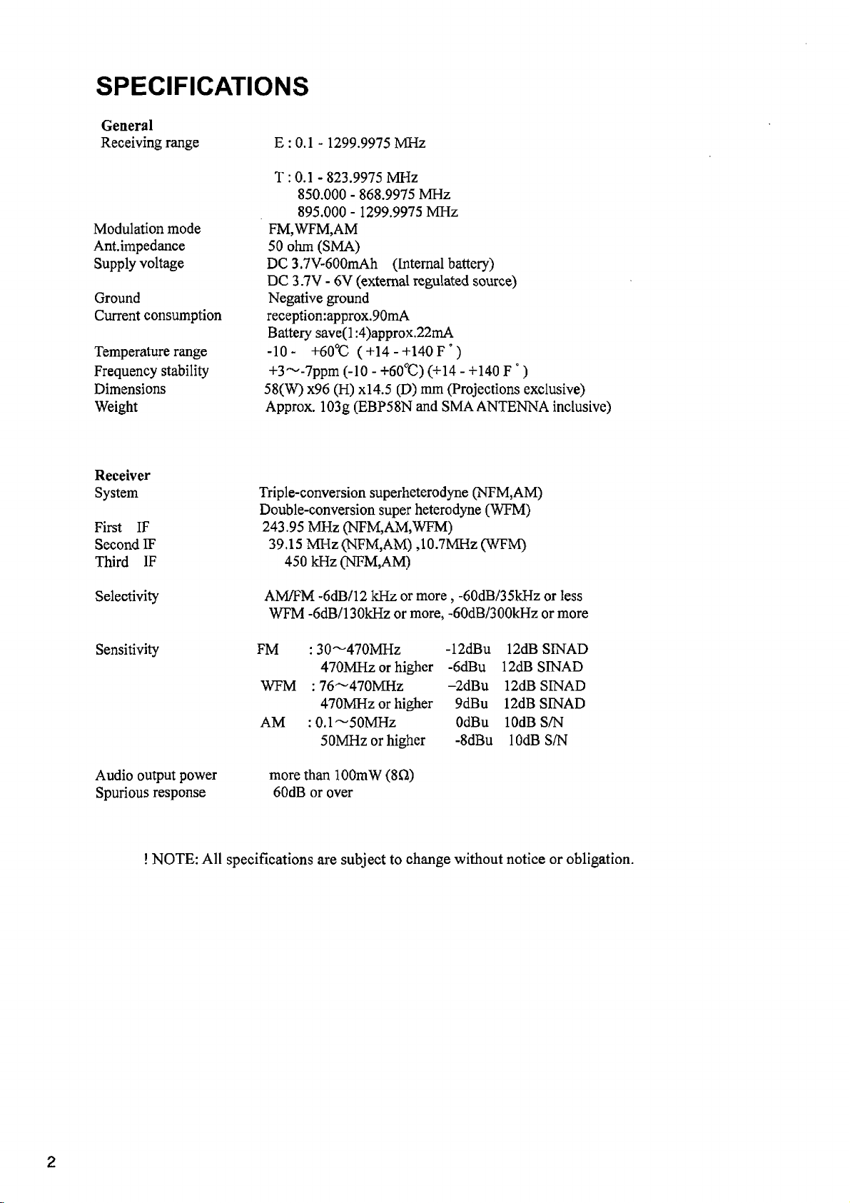
SPECIFICATIONS
G e n e r a l
Receiving range
Modulation mode
Ant. impedance
Supply voltage
Ground
Current consumption
Temperature range
Frequency stability
Dimensions
Weight
R e c e iv e r
System
First IF
Second IF
Third IF
E: 0.1 - 1299.9975 MHz
T: 0.1 -823.9975 MHz
FM,WFM,AM
50 ohm (SMA)
DC 3.7V-600mAh (Internal battery)
DC 3.7V - 6V (external regulated source)
Negative ground
reception: approx. 90mA
Battery save(l :4)approx.22mA
-10- +60°C (+14 -+140F ’)
+3~-7ppm (-10 - +60*0) (+14 - +140 F °)
58(W) x96 (H) xl4.5 (D) mm (Projections exclusive)
Approx. 103g (EBP58N and SMA ANTENNA inclusive)
Triple-conversion superheterodyne (NFM,AM)
Double-conversion super heterodyne (WFM)
243.95 MHz (NFM,AM,WFM)
39.15 MHz(NFM,AM) ,10.7MHz(WFM)
450 kHz (NFM,AM)
850.000 - 868.9975 MHz
895.000- 1299.9975 MHz
Selectivity
Sensitivity
Audio output power
Spurious response
! NOTE: All specifications are subject to change without notice or obligation.
AM/FM -6dB/12 kHz or more , -60dB/35kHz or less
WFM -6dB/l30kHz or more, -60dB/300kHz or more
FM : 30"'-'470MHz
470MHz or higher
WFM
: 76—470MHz
470MHz or higher
-12dBu 12dB SINAD
-6dBu
12dB SINAD
-2dBu 12dB SINAD
9dBu 12dB SINAD
AM :0.1~50MHz OdBu lOdB S/N
50MHz or higher
-8dBu lOdB S/N
more than lOOmW (8C2)
60dB or over
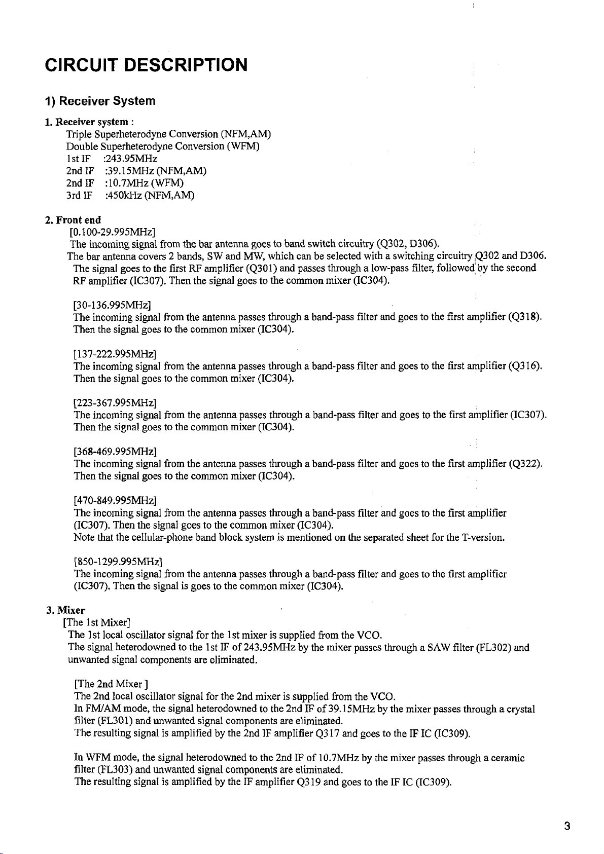
C I R C U I T D E S C R I P T I O N
1) Receiver System
1. R e c e i v e r s y s t e m :
Triple Superheterodyne Conversion (NFM,AM)
Double Superheterodyne Conversion (WFM)
1st IF :243.95MHz
2nd IF :39.15MHz (NFM,AM)
2nd IF : 10.7MHz (WFM)
3rd IF :450kHz (NFM,AM)
2. F ro n t end
[0.100-29.995MHz]
The incoming signal from the bar antenna goes to band switch circuitry (Q302, D306).
The bar antenna covers 2 bands, SW and MW, which can be selected with a switching circuitry ,Q302 and D306.
The signal goes to the first RF amplifier (Q301) and passes through a low-pass filter, followed by the second
RF amplifier (IC307). Then the signal goes to the common mixer (IC304).
[30-136.995MHz]
The incoming signal from the antenna passes through a band-pass filter and goes to the first amplifier (Q318).
Then the signal goes to the common mixer (IC304).
[137-222.995MHz]
The incoming signal from the antenna passes through a band-pass filter and goes to the first amplifier (Q316),
Then the signal goes to the common mixer (IC304).
[223-367.995MHz]
The incoming signal from the antenna passes through a band-pass filter and goes to the first amplifier (IC307).
Then the signal goes to the common mixer (IC304).
[368-469.995MHz]
The incoming signal from the antenna passes through a band-pass filter and goes to the first amplifier (Q322).
Then the signal goes to the common mixer (IC304).
[470-849.995MHz]
The incoming signal from the antenna passes through a band-pass filter and goes to the first amplifier
(IC307). Then the signal goes to the common mixer (IC304).
Note that the cellular-phone band block system is mentioned on the separated sheet for the T-version.
[850-1299.995MHz]
The incoming signal from the antenna passes through a band-pass filter and goes to the first amplifier
(IC307). Then the signal is goes to the common mixer (IC304).
3 . M i x e r
[The 1 st Mixer]
The 1st local oscillator signal for the 1st mixer is supplied from the VCO.
The signal heterodowned to the 1st IF of 243.95MHz by the mixer passes through a SAW filter (FL302) and
unwanted signal components are eliminated.
[The 2nd Mixer ]
The 2nd local oscillator signal for the 2nd mixer is supplied from the VCO.
In FM/AM mode, the signal heterodowned to the 2nd IF of 39.15MHz by the mixer passes through a crystal
filter (FL301) and unwanted signal components are eliminated.
The resulting signal is amplified by the 2nd IF amplifier Q317 and goes to the IF IC (IC309).
In WFM mode, the signal heterodowned to the 2nd IF of 10.7MHz by the mixer passes through a ceramic
filter (FL303) and unwanted signal components are eliminated.
The resulting signal is amplified by the IF amplifier Q319 and goes to the IF IC (IC309).
3
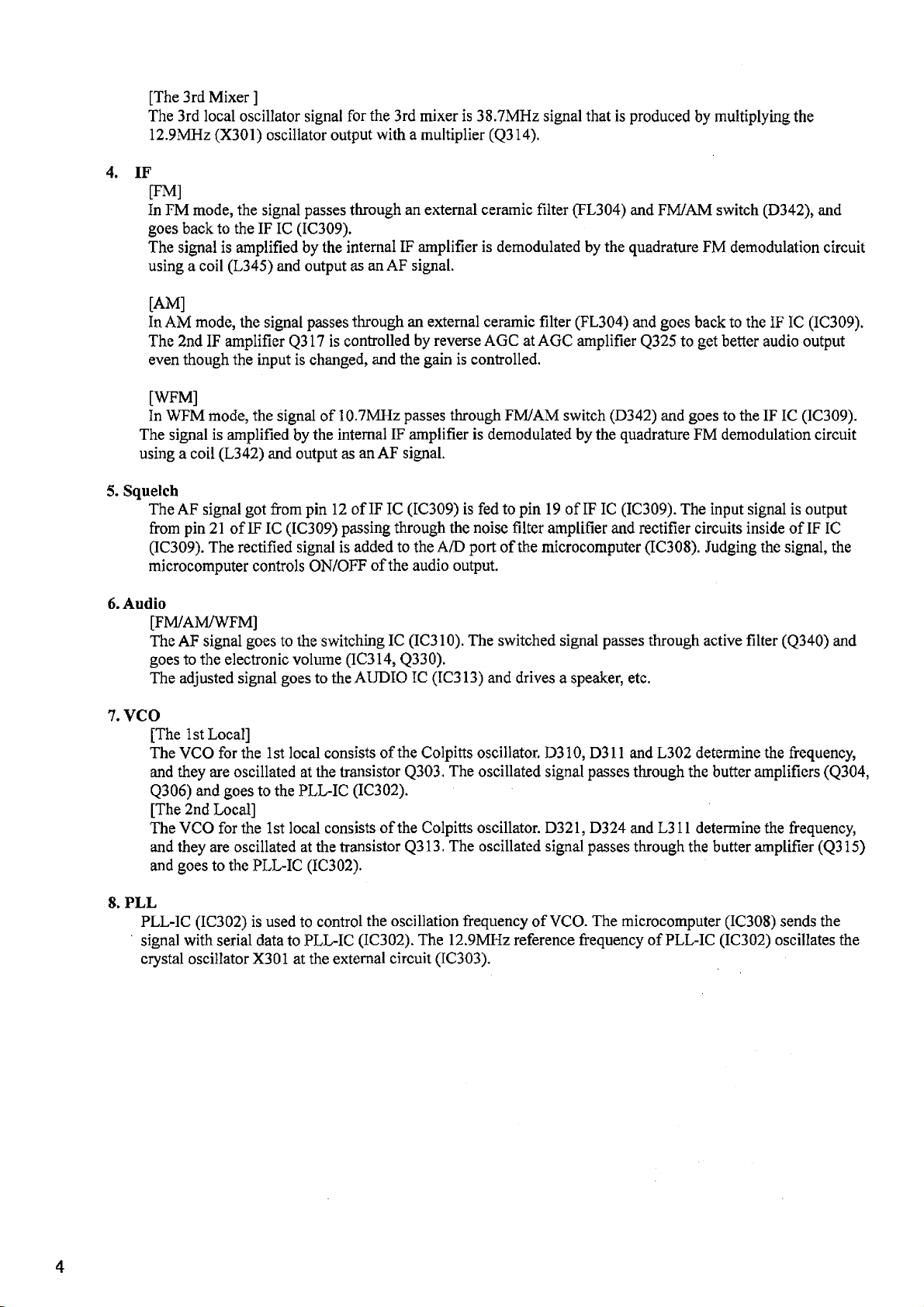
[The 3rd Mixer ]
The 3rd local oscillator signal for the 3rd mixer is 38.7MHz signal that is produced by multiplying the
12.9MHz (X301) oscillator output with a multiplier (Q314).
4 . I F
[FM]
In FM mode, the signal passes through an external ceramic filter (FL304) and FM/AM switch (D342), and
goes back to the IF IC (IC309).
The signal is amplified by the internal IF amplifier is demodulated by the quadrature FM demodulation circuit
using a coil (L345) and output as an AF signal.
[AM]
In AM mode, the signal passes through an external ceramic filter (FL304) and goes back to the IF IC (IC309).
The 2nd IF amplifier Q317 is controlled by reverse AGC at AGC amplifier Q325 to get better audio output
even though the input is changed, and the gain is controlled.
[WFM]
In WFM mode, the signal of 10.7MHz passes through FM/AM switch (D342) and goes to the IF IC (IC309).
The signal is amplified by the internal IF amplifier is demodulated by the quadrature FM demodulation circuit
using a coil (L342) and output as an AF signal.
5 . S q u e lc h
The AF signal got from pin 12 of IF IC (IC309) is fed to pin 19 of IF IC (IC309). The input signal is output
from pin 21 of IF IC (IC309) passing through the noise filter amplifier and rectifier circuits inside of IF IC
(IC309). The rectified signal is added to the A/D port of the microcomputer (IC308). Judging the signal, the
microcomputer controls ON/OFF of the audio output.
6. A u d io
[FM/AM/WFM]
The AF signal goes to the switching IC (IC310). The switched signal passes through active filter (Q340) and
goes to the electronic volume (IC314, Q330).
The adjusted signal goes to the AUDIO IC (IC313) and drives a speaker, etc.
7. V C O
[The 1st Local]
The VCO for the 1st local consists of the Colpitts oscillator,
and they are oscillated at the transistor Q303. The oscillated
D310, D311 and L302 determine the frequency,
signal passes through the butter amplifiers (Q304,
Q306) and goes to the PLL-IC (IC302).
[The 2nd Local]
The VCO for the 1st local consists of the Colpitts oscillator,
and they are oscillated at the transistor Q313. The oscillated
D321, D324 and L311 determine the frequency,
signal passes through the butter amplifier (Q315)
and goes to the PLL-IC (IC302).
8 . P L L
PLL-IC (IC302) is used to control the oscillation frequency of VCO. The microcomputer (IC308) sends the
signal with serial data to PLL-IC (IC302). The 12.9MHz reference frequency of PLL-IC (IC302) oscillates the
crystal oscillator X301 at the external circuit (IC303).
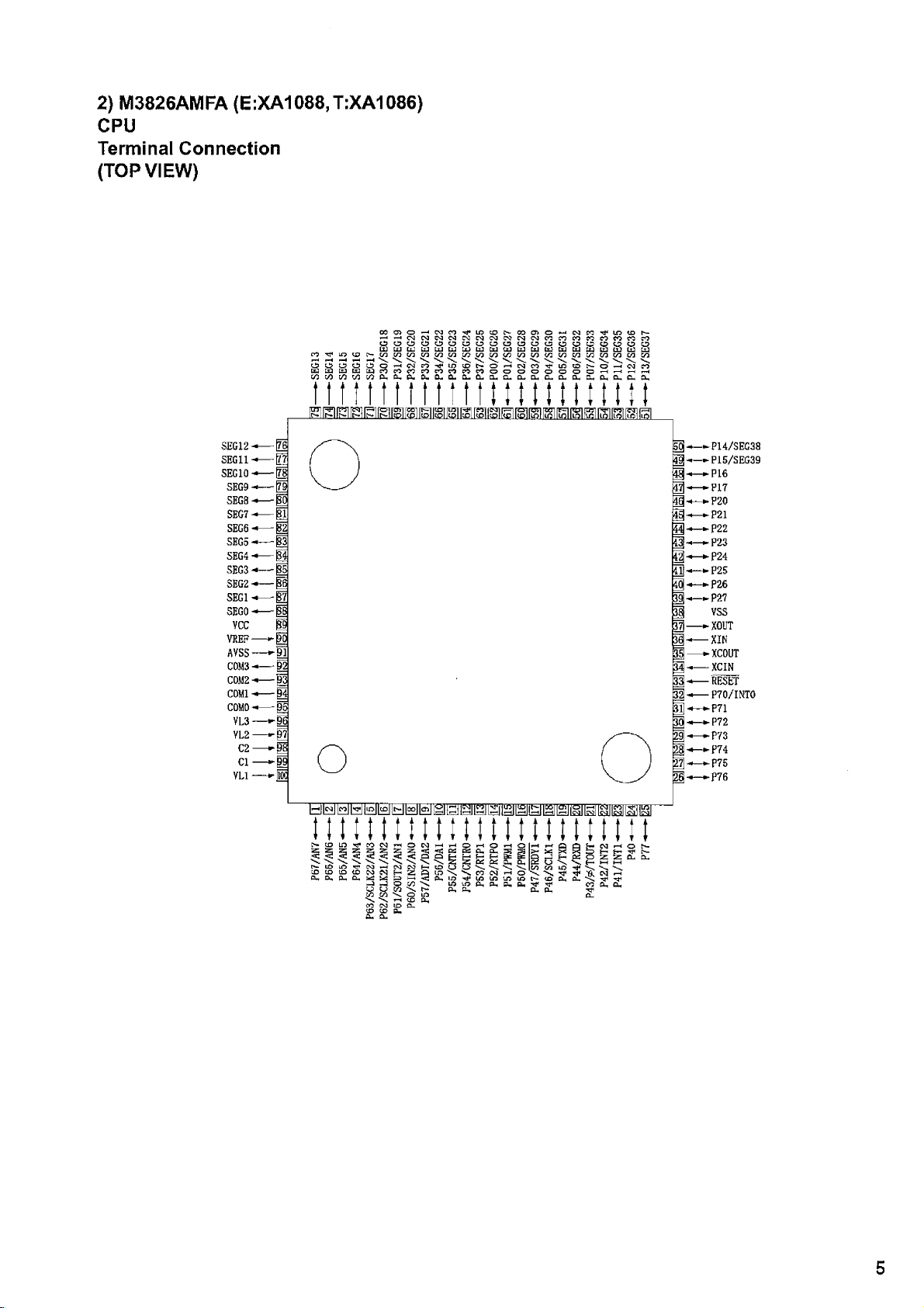
2) M3826AMFA (E:XA1088,T:XA1086)
CPU
Terminal Connection
(TOP VIEW)
C O O > O ^ N C O 'fli5 t O N C O aiO H N r t^ li5 tD N
0 0 0 0 0 0 0 0 0 0 0 0 c 3 0 0 0 0 0 0 0
«TfLOtO^WWWWWWWWWi/JWWWWCOWWWWW
.................
OOO OOO^ HCNJc O-^LO tXJt^ -
e S u a w c o r t c o c o c o r tc o rt
W0O 0O^W CL,a, O-D.O -HCLl X
[iJLtib JtiJU J b jUJtrititiJ U J tittiC tiC tittiS S tib J
...........................................................................\ N
11 i ! t f 111111 f! !l t!! I li t! t
SEG12-
SEG11-
SEG10 ■
SEG9-
SEG8-
SEG7-
SEG6-
SEG5-
SEG4-
SEG3-
SEG2-
SEG1 ■
SEGO-
VCC
VREF-
AVSS-
C0M3-
C0M2-
C0M1 ■
COMO-
VL3 ■
VL2 ■
C2
Cl-
VL1 -
o
O H C ^ r t ^ U J ^ N O
O O O O O O O O « —I —«—lr^
□m CU Cu CL, CL, Cl- 0* D-. Cu, Cu Cu, ft*
CM CO
< < K K ft, [1-
j-i pj © CO -s»
uuw\t^
[/3 w \ o in
\ \ H o a ,
rt ^ © ¡x
_ S£ S fti £3
o u u w w
lo \ ^ eo cm i-H o
___
LA IA U) U)
..ess.
-J E-m G5 o z
_
5
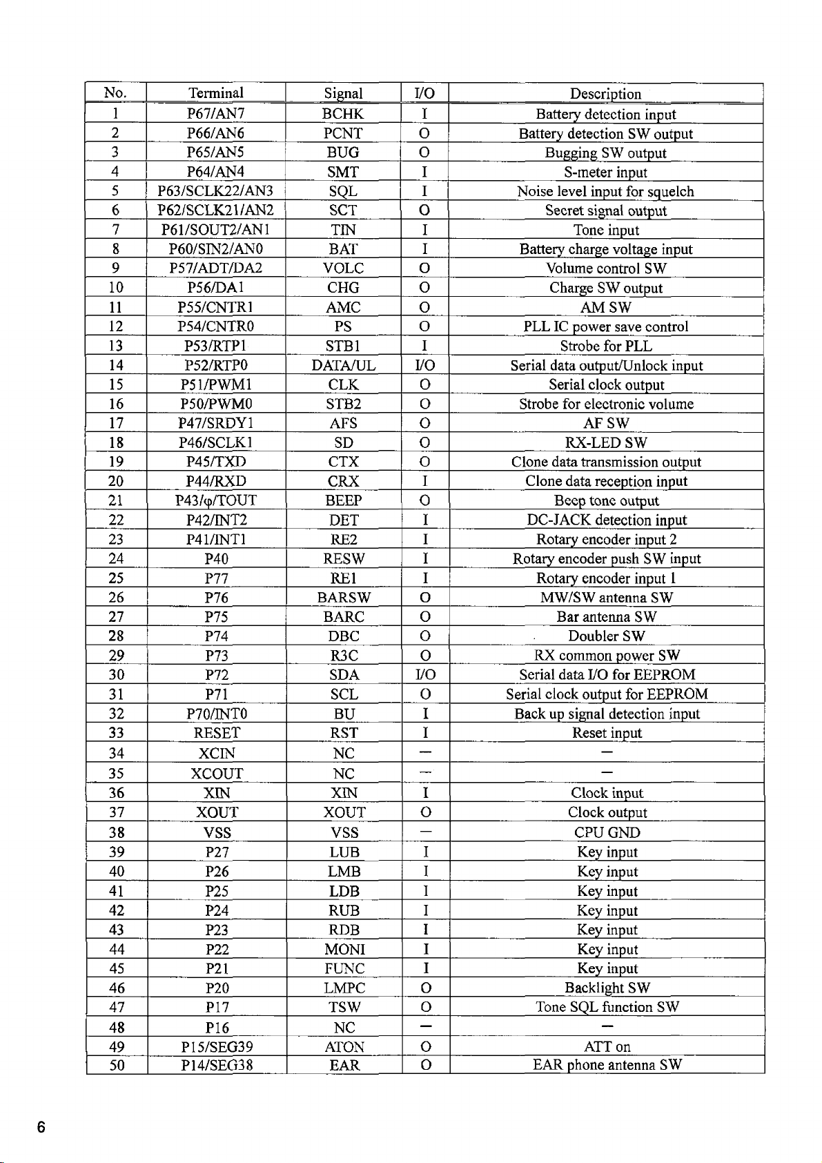
No. Terminal
1 P67/AN7
2
3 P65/AN5
4 P64/AN4
5 P63/SCLK22/AN3 SQL I
6
7
8
9 P57/ADT/DA2
10 P56/DA1
11 P55/CNTR1 AMC O AM SW
12 P54/CNTR0
13 P53/RTP1 STB1
14 P52/RTP0
15
16 P50/PWM0 STB2 O
17
18
19 P45/TXD CTX O
20
21 P43/cp/TOUT BEEP O
22
23
24
25 P77 RE1
26
27
28 P74 DBC
29
30 P72 SDA
31
32 P70/INT0
33 RESET RST I Reset input
34 XCIN NC
35 XCOUT
36
37
38
39
40
41
42
43 P23 RDB
44 P22 MONI
45 P21 FUNC
46 P20 LMPC
47 P17 TSW
48
49 P15/SEG39 ATON
50 P14/SEG38 EAR
P66/AN6
P62/SCLK21/AN2
P61/SOUT2/AN1
P60/SIN2/AN0
P51/PWM1 CLK
P47/SRDY1
P46/SCLK1
P44/RXD
P42/INT2
P41/INT1
P40 RESW
P76 BARSW
P75 BARC
P73
P71
XIN
XOUT XOUT
vss
P27
P26
P25 LDB
P24 RUB
P16
Signal VO
BCHK I
PCNT
BUG
SMT
SCT O
TIN I
BAT
VOLC
CHG
PS
DATA/UL I/O Serial data output/Unlock input
AFS O AF SW
SD O RX-LED SW
CRX
DET
RE2
R3C O
SCL O
BU
NC
XIN I Clock input
VSS
LUB
LMB I Key input
O
O
I
I
O
O
O
I
O
I
I
I
I Rotary encoder push SW input
I
O
O Bar antenna SW
O
I/O
I Back up signal detection input
— —
— —
O
—
I Key input
I
I
I Key input
I
I
Battery detection SW output
Noise level input for squelch
Battery charge voltage input
PLLIC power save control
Strobe for electronic volume
Clone data transmission output
Clone data reception input
DC-JACK detection input
Serial data VO for EEPROM
Serial clock output for EEPROM
Description
Battery detection input
Bugging SW output
S-meter input
Secret signal output
Tone input
Volume control SW
Charge SW output
Strobe for PLL
Serial clock output
Beep tone output
Rotary encoder input 2
Rotary encoder input 1
MW/SW antenna SW
Doubler SW
RX common power SW
Clock output
CPU GND
Key input
Key input
Key input
Key input
0 Backlight SW
o Tone SQL function SW
NC
—
—
o ATT on
0
EAR phone antenna SW
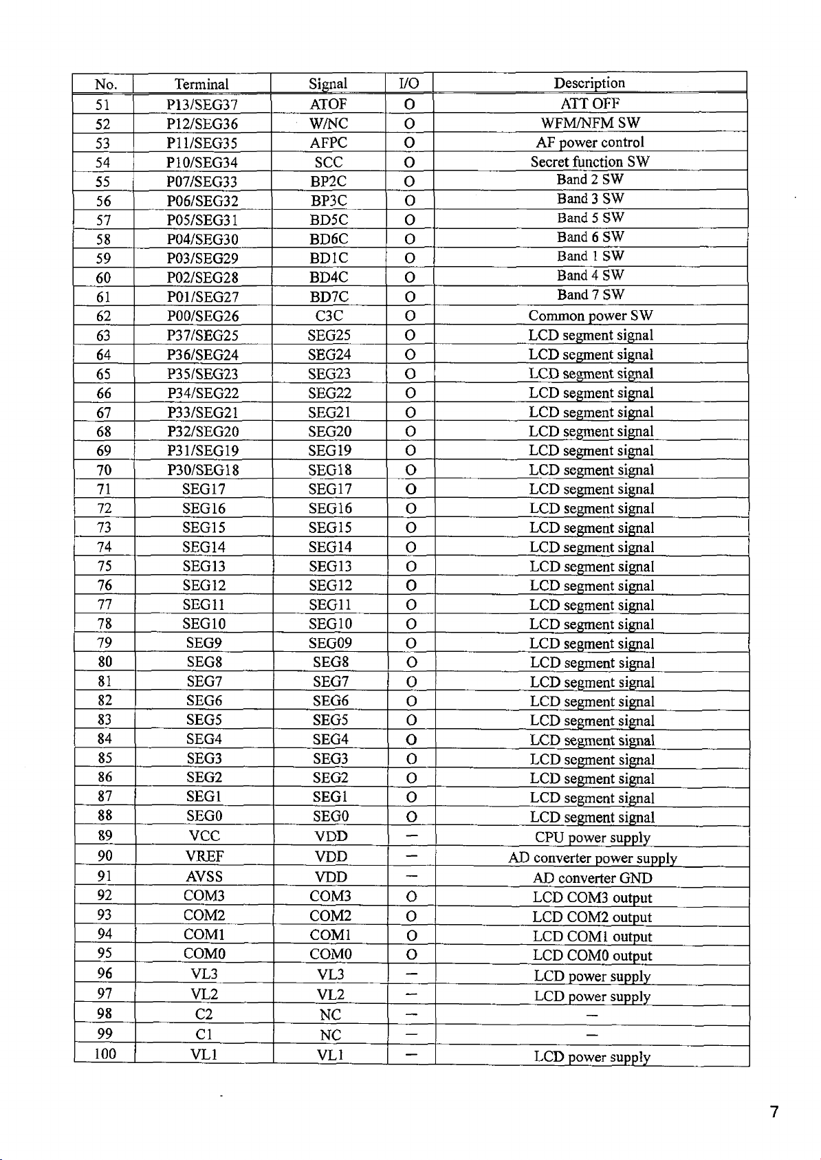
No. Terminal
51
P13/SEG37
52 P12/SEG36
53
54
55
P11/SEG35
P10/SEG34
P07/SEG33
56 P06/SEG32
57 P05/SEG31
58 P04/SEG30
59 P03/SEG29
60 P02/SEG28
61
62
P01/SEG27
P00/SEG26
63 P37/SEG25
64
P36/SEG24
65 P35/SEG23
66 P34/SEG22
67
P33/SEG21
68 P32/SEG20
69
70
71
72
73
74
75
P31/SEG19
P30/SEG18
SEG17
SEG16
SEG15
SEG14
SEG13
76 SEG12
77
78
79
80
81
82
83
84
85
86
87
88
89
SEG11
SEG10
SEG9
SEG8
SEG7
SEG6
SEG5
SEG4
SEG3
SEG2
SEG1
SEGO
vcc
90 VREF
91
92
93
94
95
96
97
98
99
100
AVSS
COM3
COM2
COMI
COMO
VL3
VL2
C2
C1
VL1
Signal
ATOF
W/NC
I/O
0
0
AFPC 0
SCC
BP2C
0
0
BP3C 0
BD5C
BD6C
BD1C
BD4C
BD7C
C3C
0
0
0
0
0
0
SEG25 0
SEG24
SEG23
SEG22
SEG21
0
0
0
0
SEG20 0
SEG19
SEG18
0
0
SEG17 o
SEG16
SEG15
SEG14
SEG13
SEG12
0
0
0
0
0
Description
ATT OFF
WFM/NFM SW
AF power control
Secret function SW
Band 2 SW
Band 3 SW
Band 5 SW
Band 6 SW
Band 1 SW
Band 4 SW
Band 7 SW
Common power SW
LCD segment signal
LCD segment signal
LCD segment signal
LCD segment signal
LCD segment signal
LCD segment signal
LCD segment signal
LCD segment signal
LCD segment signal
LCD segment signal
LCD segment signal
LCD segment signal
LCD segment signal
LCD segment signal
SEG11 0 LCD segment signal
SEG10
SEG09
SEG8
SEG7
SEG6
SEG5
SEG4
SEG3
SEG2
SEG1 0
SEGO
VDD
VDD
VDD
COM3
COM2
COMI
COMO
VL3
VL2
NC
NC
VL1
0
0 LCD segment signal
0
0
0 LCD segment signal
0
o
0
0
0
—
—
—
0
0
0
0
—
—
—
—
—
LCD segment signal
LCD segment signal
LCD segment signal
LCD segment signal
LCD segment signal
LCD segment signal
LCD segment signal
LCD segment signal
LCD segment signal
CPU power supply
AD converter power supply
AD converter GND
LCD COM3 output
LCD COM2 output
LCD COMI output
LCD COMO output
LCD power supply
LCD power supply
—
—
LCD power supply
7
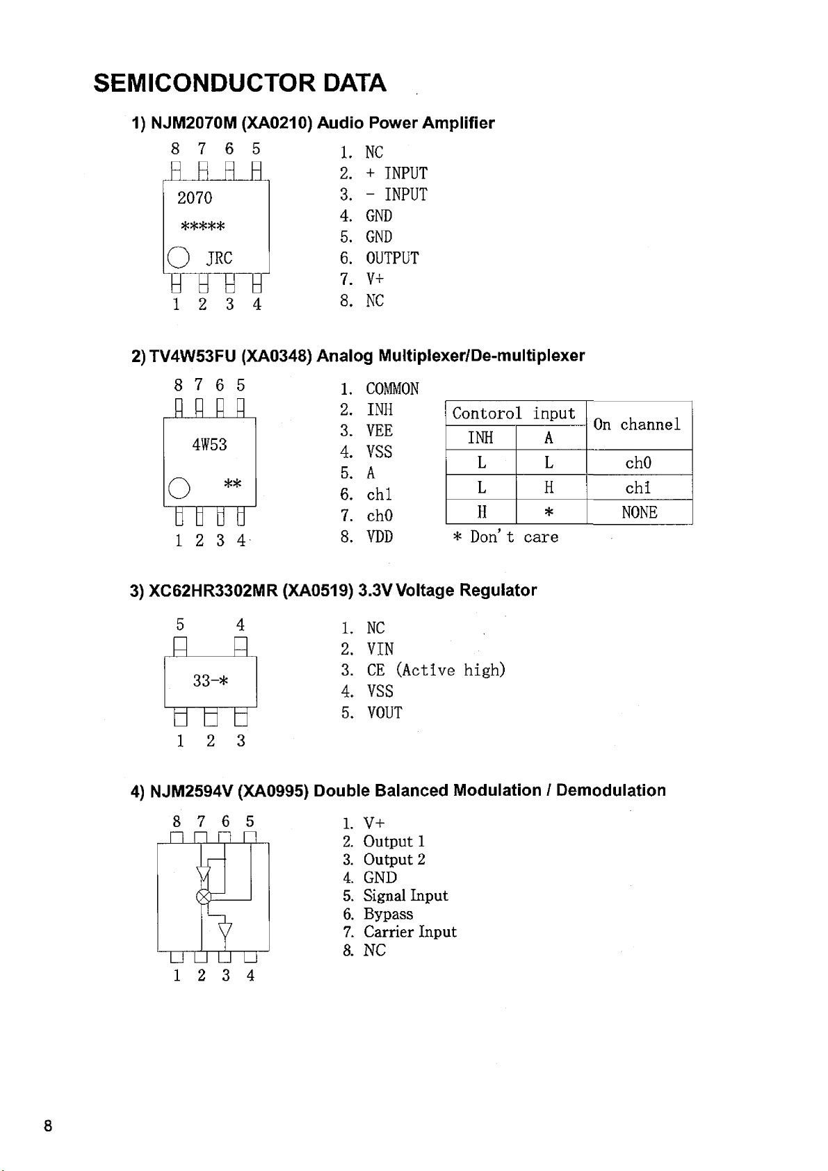
S E M I C O N D U C T O R D A T A
1) NJM2070M (XA0210) Audio Power Amplifier
8 7 6 5
R R R R
2 0 7 0
O JRC
F ÏÏ T Ï Ï
1 2 3 4
L N C
2 . + IN P U T
3 . - I N P U T
4 . G N D
5 . G N D
6 . O U T P U T
7 . V +
8 . N C
2) TV4W53FU (XA0348) Analog Multiplexer/De-multiplexer
8 7 6 5
n n r a
o
î n n n j
1 2 3 4
COMM O N
1.
2 . IN H
3 . VE E
4 . V S S
5 .
A
6 . c h i
7 . c h O
8 . VD D
C o n t o r o l i n p u t
IN H A
L L
L H
H
* D o n * t c a r e
*
O n c h a n n e l
c h O
c h i
N O N E
3) XC62HR3302MR (XA0519) 3.3V Voltage Regulator
1 . N C
2 . V I N
3 . C E ( A c t i v e h i g h )
4 . V S S
b b b
1 2 3
5 . V O U T
4) NJM2594V (XA0995) Double Balanced Modulation I Demodulation
8 7 6 5 l. V+
2. Output 1
3. Output 2
4. GND
5. Signal Input
6. Bypass
7. Carrier Input
8. NC
8
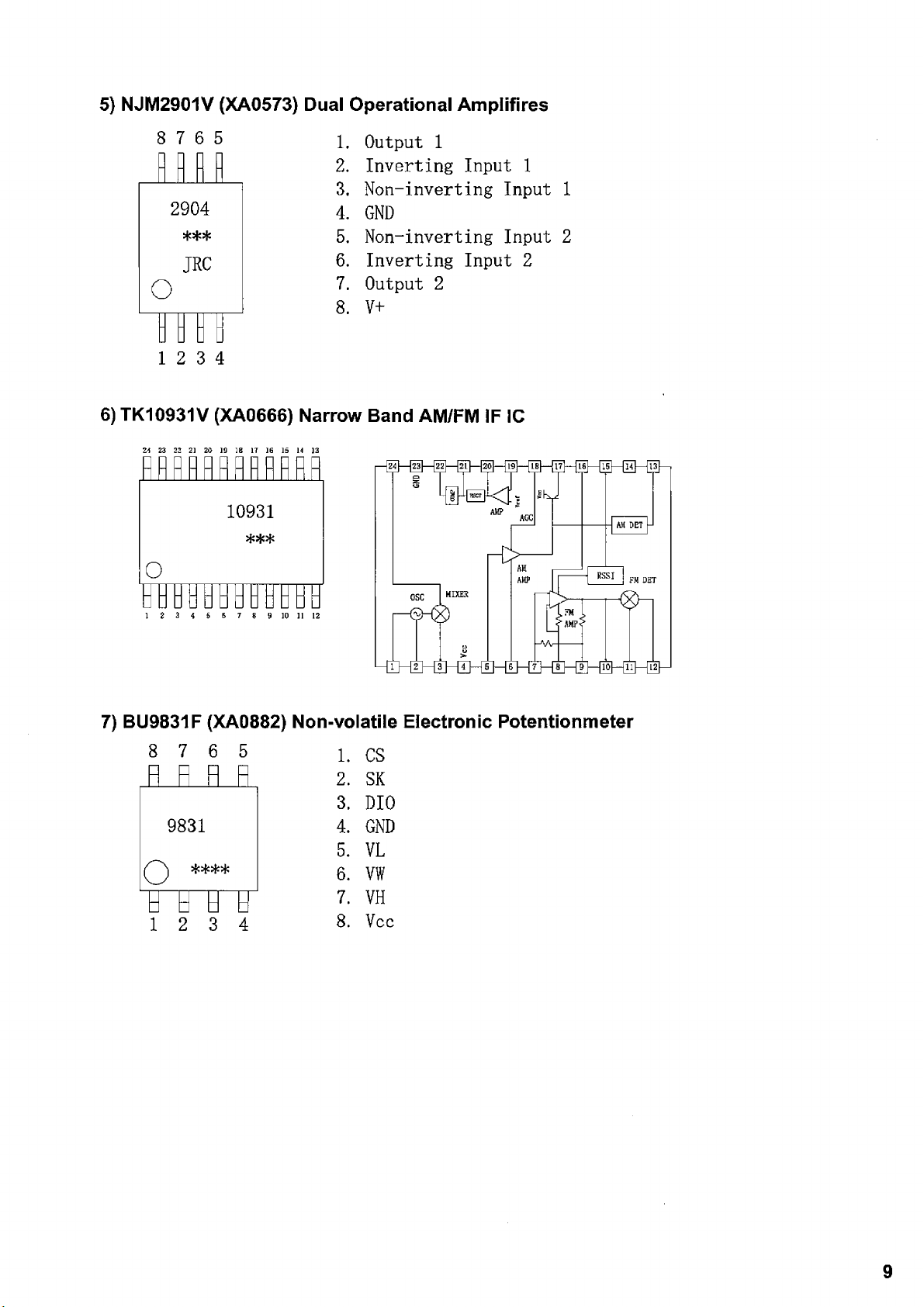
5) NJM2901V (XA0573) Dual Operational Amplifires
8 7 6 5 i' O u t p u t 1
I f
2 9 0 4
* * *
J R C
o
1 2 3 4
2 . I n v e r t i n g I n p u t 1
3 . N o n - i n v e r t i n g I n p u t 1
4 . G N D
5 . N o n - i n v e r t i n g I n p u t 2
6 . I n v e r t i n g In p u t 2
7 . O u t p u t 2
8 . V +
6) TK10931V (XA0666) Narrow Band AM/FM IF IC
24 23 22 21 20 13 18 17 16 IS 14 13
R R R H R R R R R
1 0 9 3 1
* * *
O
B T J W M M W F H
1 2 3 4 6 6 7 8 9 10 11 12
7) BU9831F (XA0882) Non-volatile Electronic Potentionmeter
8 7 6 5
R R
R
9 8 3 1
o
y
y y y
i
2 3 4
R
C S
1 .
2 . SK
3 .
D IO
4 . GND
5 . V L
6 . vw
7 .
V H
8 . V c c
9
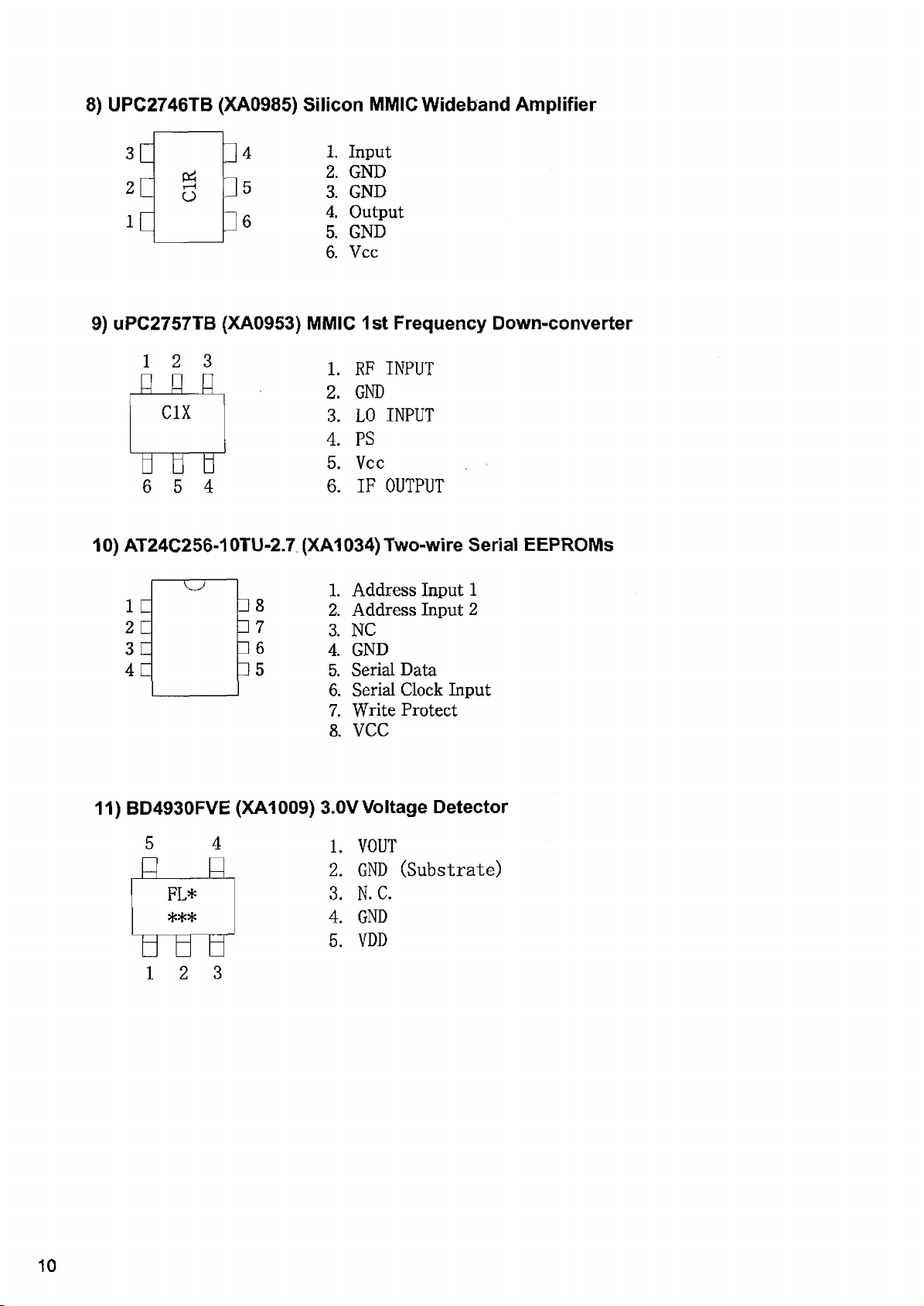
8) UPC2746TB (XA0985) Silicon MMIC Wideband Amplifier
3 E
2 L
i C
&
i—i
O
J 4
3 6
1 . Input
2. GND
GND
3.
4.
Output
GND
5.
Vcc
6.
9) uPC2757TB (XA0953) MMIC 1st Frequency Down-converter
R F IN P U T
1 .
G N D
2 .
L 0 IN P U T
3 .
P S
4 .
5 . V c c
6 . I F O U T P U T
10) AT24C256-10TU-2.7 (XA1034) Two-wire Serial EEPROMs
1. Address Input 1
1 L
2 C
3 C
4 C □ 5 5, Serial Data
^ 8 2 , Address Input 2
^ 7 3 . NC
□ 6 4. GND
6. Serial Clock Input
7. Write Protect
8. VCC
11) BD4930FVE (XA1009) 3.0V Voltage Detector
V O U T
1 .
2 . G N D
3 .
4 .
5 .
( S u b s t r a t e )
N . C .
G N D
V D D
10
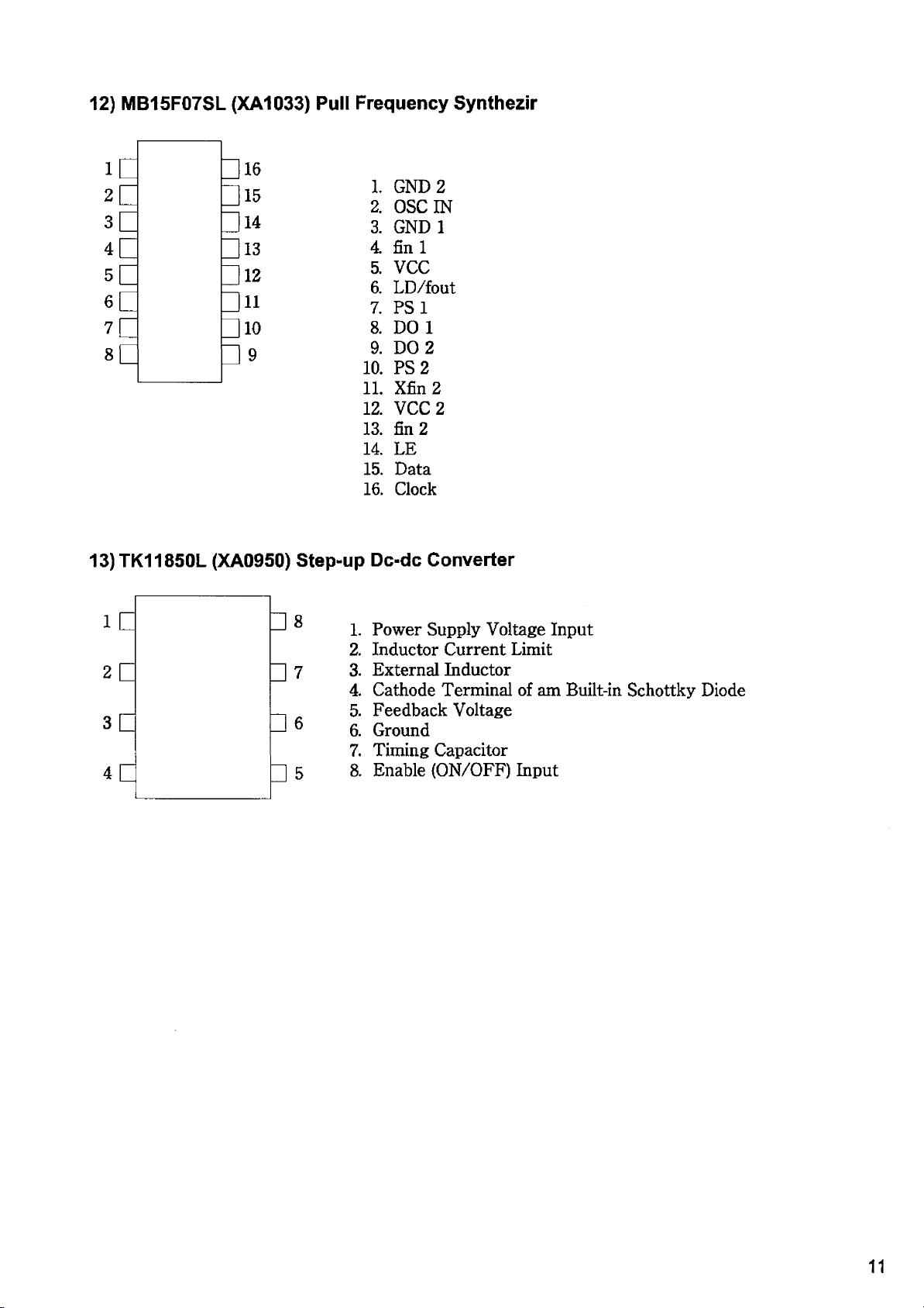
12) MB15F07SL (XA1033) Pull Frequency Synthezir
16
GND 2
15
14
13
1 2
11
1 0
9
1 .
2.
OSCIN
3. GND 1
4. fin 1
5. VCC
6.
LD/fout
7.
PS1
8. DO 1
9. DO 2
PS 2
10.
Xfin 2
11.
12. VCC 2
13. fin 2
14. LE
15. Data
16. Clock
13) TK11850L (XA0950) Step-up Dc-dc Converter
m
2 C
3 C
4 C
□ 7 3.
□ 6 a
□ 5 &
1 .
2.
4.
7.
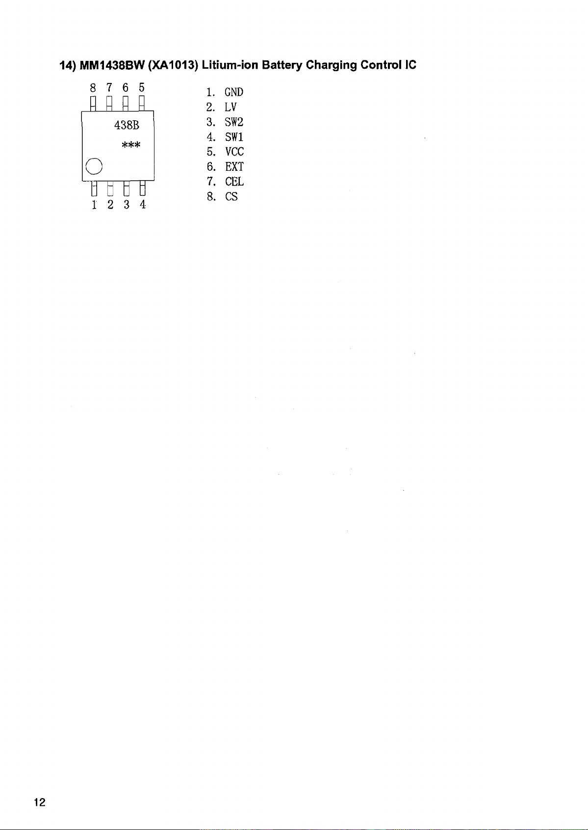
14) MM1438BW (XA1013) Litium-ion Battery Charging Control IC
8 7 6 5
w h r R
1 . G N D
2 . LV
3 . SW 2
4 . SW1
5 .
V C C
E X T
6 .
7 .
C E L
8 . CS
12
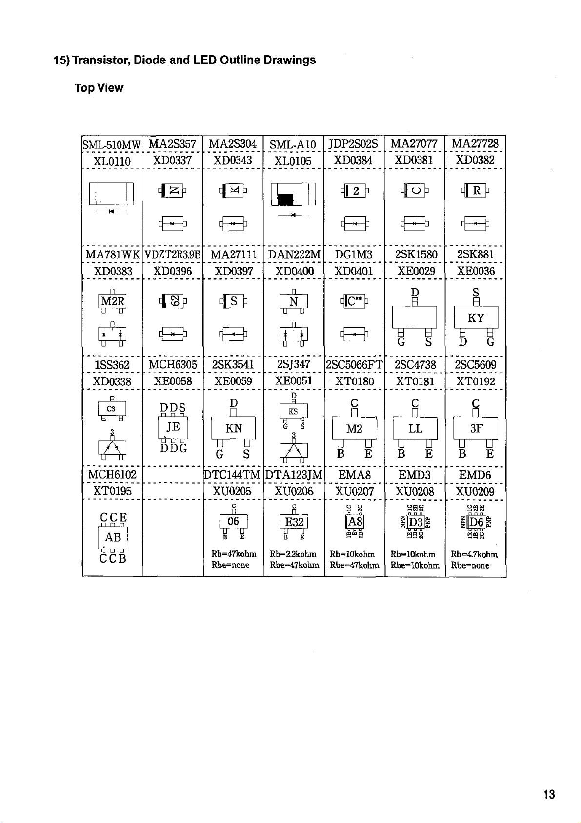
15) Transistor, Diode and LED Outline Drawings
Top View
SML-510MW
XL0110
MA2S357
XD0337
MA2S304
XD0343
MA781WK VDZT2R3.9B MA27111
XD0383
M2R
u u
XD0396 XD0397 XD0400
C D
t — H— :
ü— er
1SS362 _
XD0338
C3
B ff
□
A
U
-----
LT
MCH6102
XTÖl ’9 5 "
MCH6305
XE0058
DD S
. n n n
JE
T T Ü ' U
DDG
2SK3541
XE0059
D
ü
KN
T TGT T
DTC144TM
X U O 2Ö5" "
SML-A10
DAN222M
S
DTA123JM
"XÜÖ206 '
XL0105
-n— ,
2SJ347
XE0051
KS
Ä
JDP2S02S
XD0384
MA27077 MA27728
XD0381
DG1M3 2SK1580
XD0401
2SC5966FT
XT0180
X e 6 0 2 9
_B_
H "G" F
2SC4738
XT0181
C
X L
M2
X T
U
B
EMA8
XÜÖ207
E
X L
LL
X “
B
EMD3
XÜÖ208
XD0382
2SK881
XE0036
D
S
n
KY
X T
E ~
S
D
G
2SC5609
XTÖ192
C
C
X L
3F
u
E
X T
x r
B
EMD6
XU02Ö9
E
CCE
n n n
AB
u u u
CC B
06
u er
B E
Rb=47kohm
Rbe= none
E32
u
B E
Rb=2j2koh m
Rbe=47ko hm
A8
Rb=10 kohm
Rbe=4 7koh m
|D3 |
U LI U
Rb=1 0koh m
Rbe=10ko h m
n n n
I|D 6 |
Rb=4 .7 kohm
Rbe=n one
 Loading...