

Page 1
D J - X 3 0 T / E / K
Service Manual
C O N T E N T S
SPECIFICATIONS
General..................................
Receiver........................................................2
CIRCUIT DESCRIPTION
1) Receiver System......................................3-5
2) M30620 (E&K:XA1224B ,T:XA1232B)
SEMICONDUCTOR DATA
1) NJM2070M (XA0210)
2) TC4W53FU (XA0348)
3) TK10931V (XA0666)...................................9
4) TK11850L (XA0950)..................................10
5) uPC2757TB(XA0976)
6) NJM2594V (XA0995)
7) MB15F07SLPFV1 (XA1033)
8) TC7SZ04AFE (XA1035).............................11
9) XC62H R3002MR (XA1054)
10) BU4818FVE (XA1095).............................11
11) LM2904PWR (XA1103)............................11
12) XC6209F332MR (XA1182)
13) LC75827W (XA1183)
14) AT24C512-1.8 (XA1184)
15) BU4846FVE {XA1185).............................13
16) SM6451B (XA1186)
17) XC6371C330PR (XA1239)
18) Transistor, Diode and LED Outline Drawing
19) LCD Connection (EL0061)
.......................
.......
6-8
.................................
.................................9
...............................
................................
......................
.......................
......................
..............................
..........................13
................................
.......................
.....
.......................
10
10
10
11
12
12
13
13
14
15
EXPLODED VIEW
1) Front View................................................16
2
2) RearView
PARTS LIST
CPU Unit................................................18-19
MAIN Unit...............................................20-23
Mechanical Unit............................................23
Packing Unit.................................................23
9
ADJUSTMENT
1) Required Test Equipment..........................24
2) Entering and Releasing the Adjustment Mode
PC BOARD VIEW
SCHEMATIC DIAGRAM
BLOCK DIAGRAM...................................33
................................................
............................. 29-30
....................
.....
17
25-28
31-32
A LI N CO , Inc
Page 2
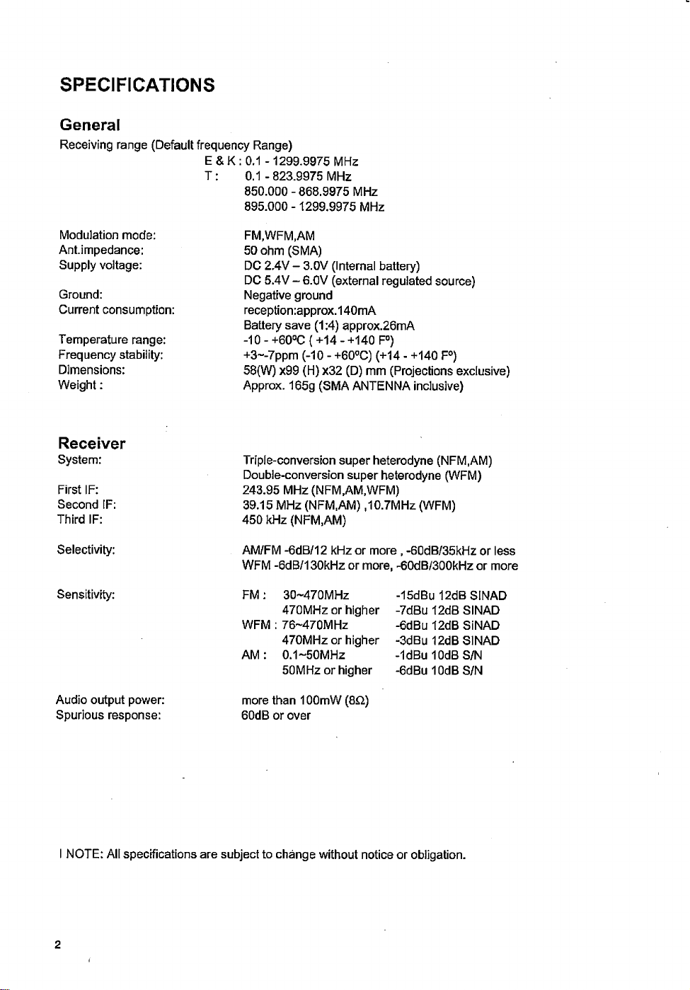
S P E C IF IC A T IO N S
General
Receiving range (Default frequency Range)
E&K: 0.1 -1299.9975 MHz
T: 0.1 -823.9975 MHz
850.000-868.9975 MHz
895.000-1299.9975 MHz
Modulation mode:
Ant.impedance:
Supply voltage:
Ground:
Current consumption:
Temperature range:
Frequency stability:
Dimensions:
Weight:
FM,WFM,AM
50 ohm (SMA)
DC 2.4V - 3.0V (Internal battery)
DC 5.4V - 6.0V (external regulated source)
Negative ground
reception :approx. 140mA
Battery save (1:4) approx.26mA
-10 - +60°C {+14 - +140 F°)
+3~-7ppm (-10 - +60°C) (+14 - +140 F°)
58(W) x99 (H) x32 (D) mm (Projections exclusive)
Approx. 165g (SMA ANTENNA inclusive)
Receiver
System:
First IF:
Second IF:
Third IF:
Selectivity:
Sensitivity: FM :
Triple-conversion super heterodyne (NFM.AM)
Double-conversion super heterodyne (WFM)
243.95 MHz (NFM,AM,WFM)
39.15 MHz (NFM.AM) ,10.7MHz (WFM)
450 kHz (NFM.AM)
AM/FM -6dB/12 kHz or more , -60dB/35kHz or less
WFM -6dB/130kHz or more, -60dB/300kHz or more
WFM : 76~470MHz
AM: 0.1~50MHz
30~470MHz
470MHz or higher
470MHz or higher
50MHz or higher
-15dBu 12dB SINAD
-7dBu 12dB SINAD
-6dBu 12dB SiNAD
-3dBu 12dB SINAD
-1dBu 10dB S/N
-6dBu 10dB S/N
Audio output power:
Spurious response:
I NOTE: All specifications are subject to change without notice or obligation.
more than 10OmW (8£2)
60dB or over
Page 3
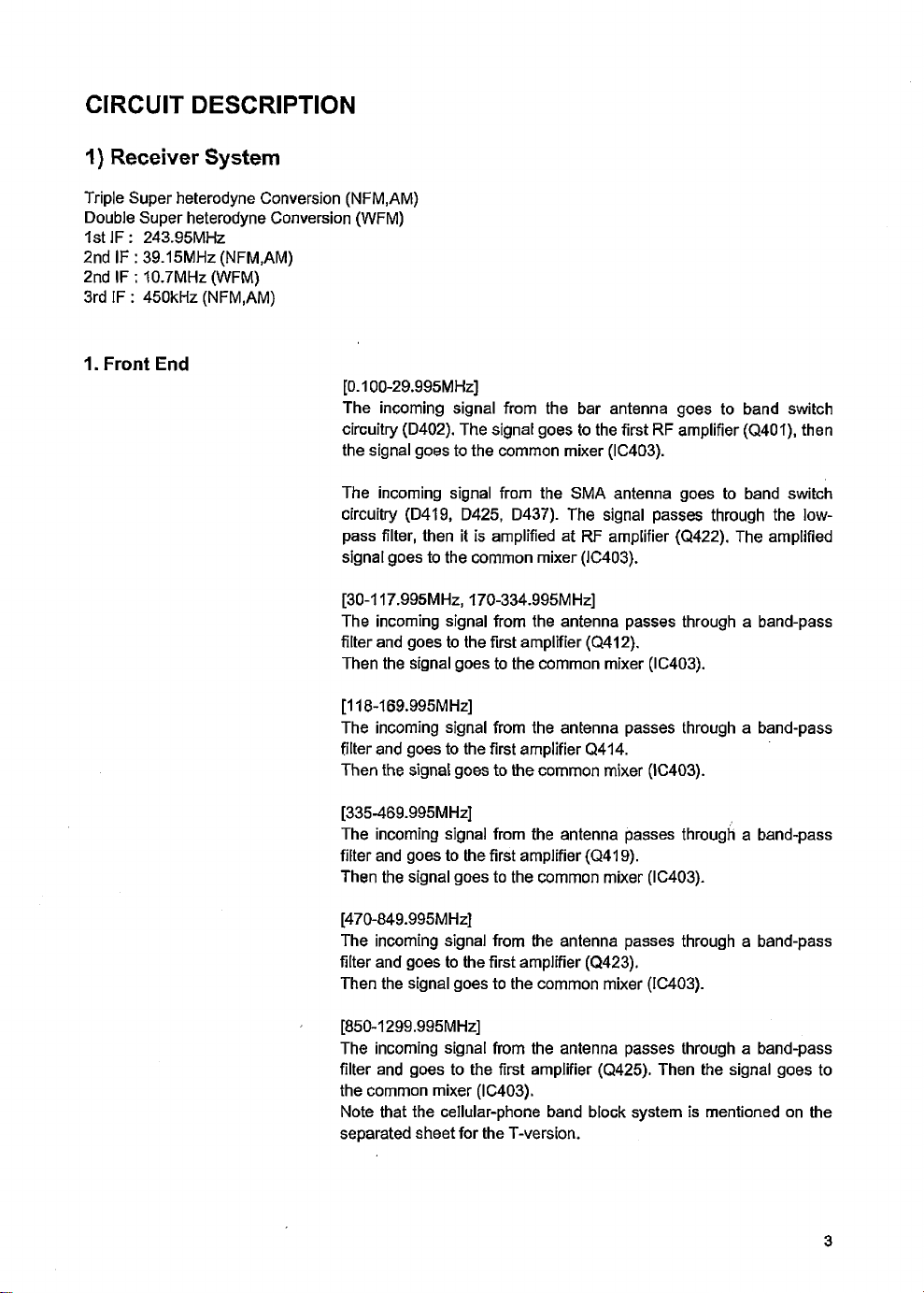
C IR C U IT D E S C R IP T IO N
1) Receiver System
Triple Super heterodyne Conversion (NFM.AM)
Double Super heterodyne Conversion (WFM)
1st IF: 243.95MHz
2nd IF: 39.15MHz (NFM.AM)
2nd IF : 10.7MHz (WFM)
3rd IF : 450kHz (NFM.AM)
1. Front End
[0.100-29.995MHz]
The incoming signal from the bar antenna goes to band switch
circuitry (D402). The signal goes to the first RF amplifier (Q401), then
the signal goes to the common mixer (IC403).
The incoming signal from the SMA antenna goes to band switch
circuitry (D419, D425, D437). The signal passes through the low-
pass filter, then it is amplified at RF amplifier (Q422). The amplified
signal goes to the common mixer (IC403).
[30-117.995MHz, 170-334.995MHz]
The incoming signal from the antenna passes through a band-pass
filter and goes to the first amplifier (Q412).
Then the signal goes to the common mixer (IC403).
[118-169.995MHz]
The incoming signal from the antenna passes through a band-pass
filter and goes to the first amplifier Q414.
Then the signal goes to the common mixer (IC403).
[335-469.995MHz]
The incoming signal from the antenna passes through a band-pass
filter and goes to the first amplifier (Q419).
Then the signal goes to the common mixer (IC403).
[470-849.995M Hz]
The incoming signal from the antenna passes through a band-pass
filter and goes to the first amplifier (Q423).
Then the signal goes to the common mixer (IC403).
[850-1299.995MHz]
The incoming signal from the antenna passes through a band-pass
filter and goes to the first amplifier (Q425). Then the signal goes to
the common mixer (IC403).
Note that the cellular-phone band block system is mentioned on the
separated sheet for the T-version.
3
Page 4
2. Mixer
3. IF
[The 1st Mixer]
The 1st local oscillator signal for the 1st mixer is supplied from the
VCO.
The incoming signal to the 1st mixer (IC403) and the 1st local signal
are added or subtracted at mixer (IC403), and the SAW filter (FL402)
selects the signal of 243.95MHz, then it goes to the 2nd mixer
(IC404) after the adjacent signal is eliminated.
[The 2nd Mixer]
The 2nd local oscillator signal for the 2nd mixer is supplied from the
VCO.
{FM/AM}
In FM/AM mode, the signal heterodowned to the 2nd IF of 39.15MHz
by the mixer passes through a crystal filter (FL401) and unwanted
signal components are eliminated.
The resulting signal is amplified by the 2nd IF amplifier Q413 and
goes to the IF ]C (IC406).
{WFM}
In WFM mode, the signal heterodowned to the 2nd IF of 10.7MHz by
the mixer passes through a ceramic filter (FL403) and unwanted
signal components are eliminated.
The resulting signal is amplified by the IF amplifier Q416 and goes to
the IF IC (IC406).
[The 3rd Mixer]
The 3rd local oscillator signal for the 3rd mixer is 38.7MHz signal that
is produced by multiplying the 12.9MHz (X401) oscillator output with
a multiplier (Q411).
[FM]
In FM mode, the signal passes through an external ceramic filter
(FL404) and FM/AM switch D440, and goes back to the IF IC
(IC406).
The signal is amplified by the internal IF amplifier is demodulated by
the quadrature FM demodulation circuit using a coil (L445) and
output as an AF signal.
[AM]
In AM mode, the signal passes through an external ceramic filter
(FL404) and goes back to the IF IC (IC406).
The 2nd IF amplifier (Q413) and RF amplifier (Q414) is controlled by
reverse AGC at AGC amplifier Q420 to get better audio output even
though the input is changed, and the gain is controlled.
[WFM]
In WFM mode, the signal of 10.7MHz passes through FM/AM switch
(D440) and goes to the IF IC (IC406).
The signal is amplified by the internal IF amplifier is demodulated by
the quadrature FM demodulation circuit using a coil (L442) and
output as an AF signal.
4
Page 5
4. Squelch The AF signal got from pin 12 of IF IC (IC406) is fed to pin 19 of IF IC
(IC406). The input signal is output from pin 21 of IF IC (IC406)
passing through the noise filter amplifier and rectifier circuits inside of
IF IC (IC406). The rectified signal is added to the A/D port of the
microcomputer (IC203). Judging the signal, the microcomputer
controls ON/OFF of the audio output.
5. Audio
[FM/AM/WFM]
The AF signal goes to the switching IC (IC407). The switched signal
passes through active filter (Q213) and goes to the electronic volume
(1C216).
The adjusted signal goes to the AUDIO IC (IC215) and drives a
speaker, etc.
6.VCO
[The 1st Local]
The VCO for the 1st local consists of the Colpitts oscillator. D406,
D409 and L403 determine the frequency, and they are oscillated at
the transistor Q402. The oscillated signal passes through the buffer
amplifiers (Q403, Q404) and goes to the PLL-IC (IC401).
[The 2nd Local]
The VCO for the 1st local consists of the Colpitts oscillator. D424,
D426 and L410 determine the frequency, and they are oscillated at
the transistor Q409. The oscillated signal passes through the butter
amplifier (Q410) and goes to the PLL-IC (IC401).
7. PLL
PLL-IC (IC401) is used to control the oscillation frequency of VCO.
The microcomputer (1C203) sends the signal with serial data to PLL-
IC (1C401). The 12.9MHz reference frequency of PLL-IC (IC401)
oscillates the crystal oscillator (X401) at the external circuit (IC402).
5
Page 6
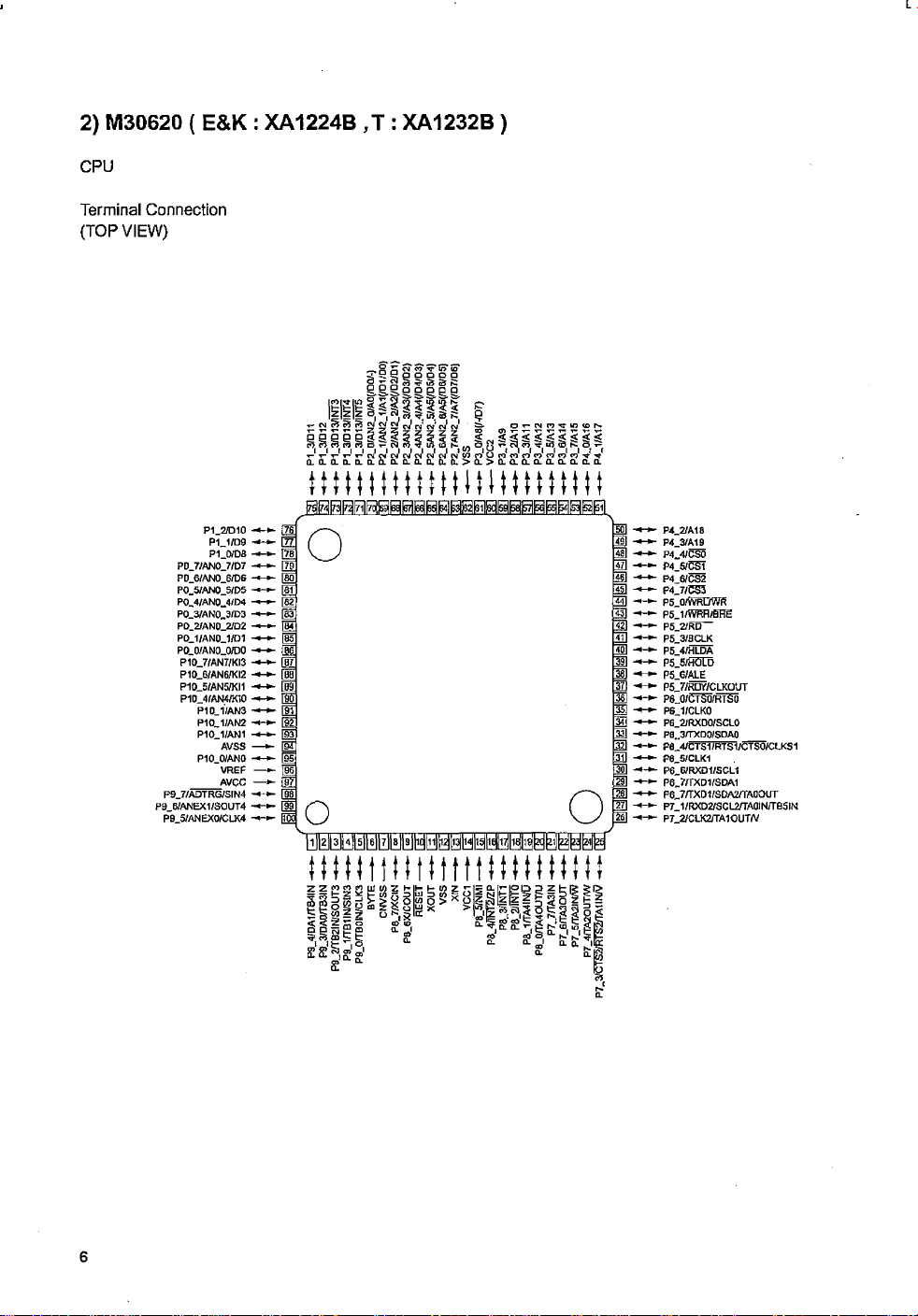
2) M30620 ( E&K : XA1224B ,T : XA1232B )
CPU
Terminal Connection
(TOP VIEW)
Z E E e'eV s W s'siV s > £ S 2 £ £ £ £ £ £ Sf2
ttttttttttHtttlttttttttt
L
P1 2Æ310
P1J/D9
P1_0/DS
PD_7/AN0_7/D7
PO_6/ANO_6/D6
PO_5/ANO_5/D5
PO_4/ANO_4iD4
P0_3/AN0_3©3
PO_2/ANO_2/D2
PO_1/ANO_1/D1
P0_0/ANO_0/D0
P10_7/AN7/KI3
P10_6/AN6/KI2
P10_5/AN5/KI1
P10_4/AN4/KI0
P10_iiAN3
P10_1/AN2
P10_1/AN1
AVSS
P10JVAN0
VREF
P9.7/ADTRG/SIN4
P9 6/ANEX1/SOUT4
P9 5/ANEX0/CLK4
AVCC
P4_2/A18
P4_3/A19
P4_4/CS0
P4_5/55t
P4_6/CS2
P4_7/CS3
P5_0/WRL/WR
P5_1/WRH/BHg
P5_2/RD
P5_3/BCLK
P5_4/HLDA
PS 5/fiÜEÖ
PS_6/ALH
P5JVRDY/CLKOUT
P6„0/CTSÜ/rTSÖ
P6.1/CLK0
P6_2/RXD0/SCL0
PB J3/TXD0/SDA0
Pfl_4/CTS1/RTS1/CTS0/CLKS1
P6_5/CLK1
P6_6/RXOt/SCL1
P6_7fTXD1/SDA1
P6„7n'XD1/SDA2/TAOOUT
P7_1 /RXD2/SCL2/TA01N/T0S IN
P7_2/CLK2/TA10UT/V
6
Page 7
No.
1
2
3
4
5
6
7
8
9
10
11
12
13
14
15
16
17
18
19 P8 1
20
21
22
23 P7 5
24
25
26
27
28 P7 0
29
30 RXD1
31 P6_5
32
33
34
35 P6 1
Terminal Signal | I/O
P9 3
DAO
P9 2
NC -
TRC 1 0
BUGC O
P9_l WFC
P9„0
BYTE
CNVSS
XCIN
XCOUT
RESET
XOUT
v ss
XIN
VCC1
NMI
INT2
SCO
VSS
v ss
NC
NC
RESET
XOUT
VSS
XIN I
VDD
VDD
BU I
INTI PWR
INTO
RE1
RE2
P8_0
P7_7
TA30UT
SCT
RESW I
BEEP
MONI
P7 4
P7 3
P7 2
P7_l
FNC I
RCSW I
AFS 0
CLNC 0
NC
TXD1 TXD
RXD I
NC
P6_4
TXDO
RXDO
RECSW
SDA
SCL
BLLMP
36 P6 0 INT
37
38
39 P5 5
40
41
42
43
44
45
46
47 P4 5
48 P4 4
P5 7
P5_6
P5 4
P5_3
P5 2
P5_l
P5 0
P4_7
P4_6
CLK I/O
DATA
R3C
NFC 0
BF6C
DB2C
BF5C 0
LCONT 0
DB3C
STB2
AFPC
TONE 0
49 P4 3 MIDO
50 P4 2
AKA
Description
—
Tracking control
Bugging SW output
0 WFM SW
0 Secret function SW
—
-
CPU GND
CPUGND
— —
—
I
—
Reset input
0 Clock output
—
CPUGND
Clock input
—
—
Power supply
Power supply
Back up signal detection input
I
I
POWER key input
Rotary encoder input 1
I Rotary encoder input 2
0 Secret signal output
Rotaiy encoder push SW input
0
Beep tone output
I MONI key input
FUNC key input
Remote controller AF SW
AF SW
Clone SW
—
0
Clone data transmission output
—
Clone data reception input
—
—
—
—
—
—
—
—
0 Backlight SW
-
—
Serial clock I/O for EEPROM
I/O
Serial data I/O for EEPROM
0 RX common power SW
NFMSW
0
BND6 power SW output
0 Doubler2 SW
BND5 power SW output
LCD driver control
0 Doubler3 SW
0 Strobe for LCD driver
0 AF power control
AF tone control
0 Green LED SW
0 Red LED SW
7
Page 8
No.
51
52
53 P3 7
54
55 P3 5
56 P3 4
57
58 P3_2
59
60 VCC2
61
62
63
64
65
66
67 AN2 3
68
69 AN2„1
70
71
72
73 PI 5
74
75 PI 3
76 PI 2
77
78
79 P0 7
80
81 P0 5
82 P0_4
83 PO_3
84 P0 2
85 P0_1
86 PO 0
87 P10_7
88 P10 6 KI1
89 P10 5
90 P10 4
91
92 AN2
93 AN1
94
95 ANO
96
97 AVCC
98 P9 7
99 P9_6 CHG o
100
Terminal
P4_l
P4 0
P3 6
P3„3
P3_l
P3 0
v s s
P2_7
P2_6 ABRC
P2_5 .
AN2„4
AN2 2
AN2 0
Pl_7
PI 6
Pl_4
Pl-1
P1_0
P0_6 PLC
AN3 CDET
AVSS
VREF
P9_5 AMC 0
Signal
DB1C 0
AT2C
EARC
TNC 0
STB1
DATA
CLK 0
PS
STB3 0
VDD
NC
VSS
SBRC 0
ATONC 0
TIN I
ADIN
SOL I
SMT
BCHK I
DCDET I
RAC
BF4C
ATOFC 0
CNT 0
BF3C 0
BF2C 0
BF1C 0
AT1C 0
RECC
KSC
K03
K02
KOI
KOO
KI2
KI0 I
KI3 I
BP1
BP2 I
VSS
NC
VDD
VDD
EVC o
I/O
—
0
0
I/O
0
—
—
—
0
—
0
0
—
—
0
0
0
0
I
I
I
—
—
—
—
Description
Doublerl SW
—
Earphone antenna SW
Tone SQL function SW
Strobe for PLL
Serial data output/Unlock input
Serial clock output
PLL IC power save control
Strobe for Evol
Power supply
—
CPU GND
SW BAR antenna control
AM BAR antenna control
ATT ON control
Tone input
I
I
Remote controller SW level input
Noise level input for squelch
S-meter input
Power supply level input
External supply level input
—
BND4 power SW output
ATT OFF control
Battery detection SW output
BND3 power SW output
BND2 power SW output
BND1 power SW output
ATT SW
PLL IC power SW
—
—
Key matrix output
Key matrix output
Key matrix output
Key matrix output
Key matrix input
Key matrix input
Key matrix input
Key matrix input
Battery Voltage input
BAND PLAN 1 input
BAND PLAN 2 input
CPU GND
—
Power supply
Power supply
Evol power control
Charge function SW
AM SW
8
Page 9
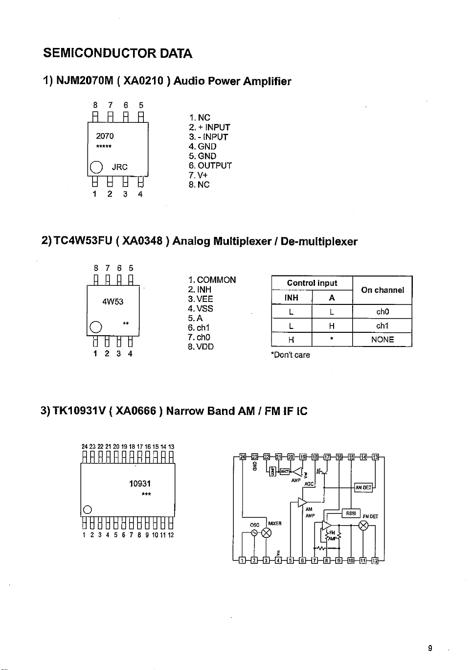
SEMICONDUCTOR DATA
1) NJM2070M ( XA0210 ) Audio Power Amplifier
8 7 6 5
R R R R
1 2 3 4
2)TC4W53FU ( XA0348 ) Analog Multiplexer / De-multiplexer
1.NC
2. + INPUT
3.-INPUT
4. GND
5.GND
6. OUTPUT
7.V+
8.NC
1 2 3 4
1. COMMON
2. INH
3.VEE
4.VSS
5. A
6. ch1
7. chO
8.VDD
Control input
INH A
L
L H ch1
H
‘Don't care
3) TK10931V ( XA0666 ) Narrow Band AM / FM IF IC
24 23 22 21 201918 171615 14 13
HRRHRHHHHRHH
10931
***
M M Ï Ï Ï Ï Ï Ï ÏÏ Ï Ï Ï Ï
1 2 3 4 5 6 7 8 9 10 11 12
On channel
L
★
chO
NONE
9
Page 10
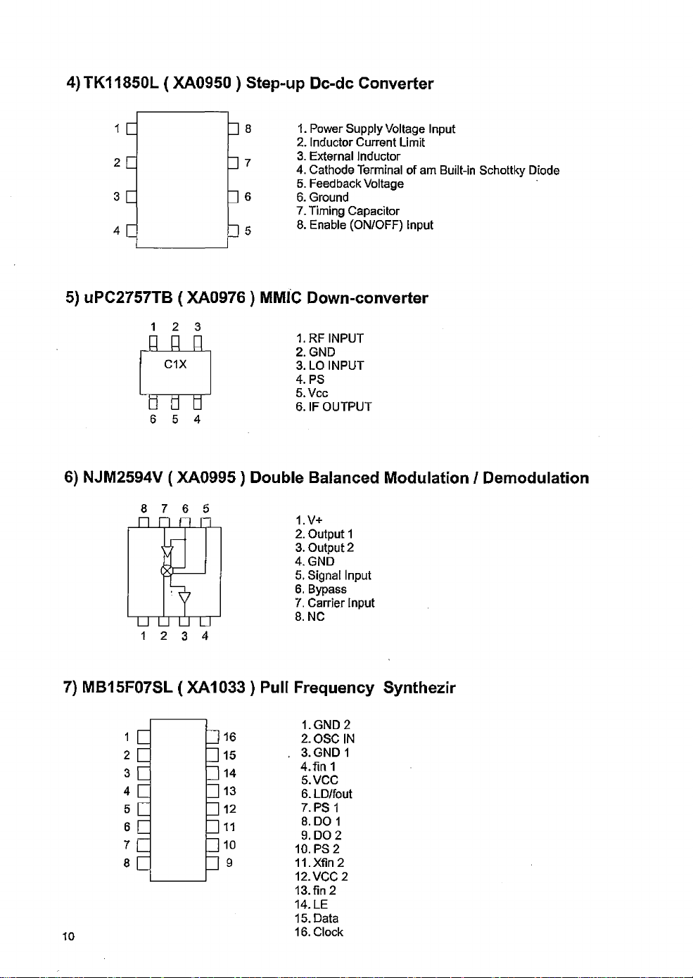
4)TK11850L ( XA0950 ) Step-up Dc-dc Converter
1 E
□ 8
1. Power Supply Voltage Input
2. Inductor Current Limit
2 C
□ 7
3. External Inductor
4. Cathode Terminal of am Built-in Schottky Diode
5. Feedback Voltage
3 C
□ 6
6. Ground
7. Timing Capacitor
4 C
□ 5
8. Enable (ON/OFF) Input
5) UPC2757TB (XA0976 ) MMIC Down-converter
1 2 3
a n n
1.RF INPUT
2.GND
3. LO INPUT
4. PS
5. Vcc
6. IF OUTPUT
6) NJM2594V (XA0995) Double Balanced Modulation / Demodulation
8 7 6 5
n n n n
T J U L T L J
1 2 3 4
1.V+
2. Output 1
3. Output 2
4.GND
5. Signal Input
6. Bypass
7. Carrier Input
8.NC
7) MB15F07SL ( XA1033 ) Pull Frequency Synthezir
1.GND2
2. OSC IN
3. GND 1
4. fin 1
5. VCC
6. LD/fbut
7. PS 1
8. DO 1
9. DO 2
10. PS 2
11. Xfin 2
12. VCC 2
13. fin 2
14. LE
15. Data
16. Clock
10
1 □
2 C
3 C
4 □
5 □
6 C
7(1
8 □
□ 16
□ 15
□ 14
□ 13
□ 12
□ 11
□ 10
□ 9
Page 11
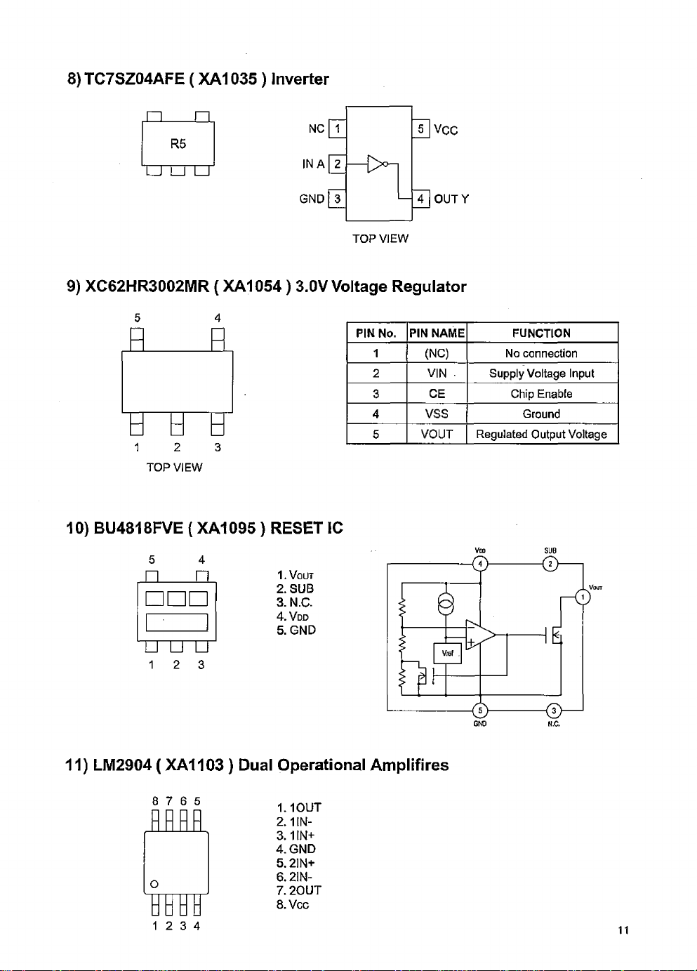
8) TC7SZ04AFE ( XA1035 ) Inverter
n n
NC 1
5
Vcc
R5
2
u u u
IN A
GND 3
I— 4
4 OUTY
TOP VIEW
9) XC62HR3002MR ( XA1054) 3.0V Voltage Regulator
PIN No.
TOP VIEW
PIN NAME FUNCTION
1
2
3
4
5
(NC) No connection
VIN ■ Supply Voltage Input
CE Chip Enable
VSS
VOUT Regulated Output Voltage
Ground
10) BU4818FVE (XA1095 ) RESET IC
1. VOUT
2. SUB
3. N.C.
dd
4. V
5.GND
11) LM2904 ( XA1103) Dual Operational Amplifires
8 7 6 5 1.10UT
2.11N-
3.1 IN+
4. GND
5.21N+
6.21N-
7.20UT
8. Vcc
1 2 3 4
11
Page 12

12) XC6209F332MR ( XA1182 ) 3.3V Voltage Regulator
1 .V 1N
2. Vss
3. CE
4. NC
5. Vout
13) LC75827W ( XA1183 ) LCD Display Driver
T V \ n W I l - l A f 0 0 N I D m t W ( M i - O 0 ) ( 0 S S ) U ) \ f n
U r V tVV
S49
S50
S51/COM4
COM3
COM2
COM1
Vdd
VLCD
VLCD1
VLCD2
vss
OSC
INH
CE □ Z
CL
DI
ww MwramrawBJfflio toiOB iBto
ARRRRRRRRRRRRRRR
49
¡O
e r
□ z
i= q
□ c
□ =
□=
□ =
e r
LJ_
□ Z
□=
□=
□=
rr~
rr~
64I
!/■
32
t l
- L J S32
U Z S31
z a S30
= □ S29
Z L J S 28
= □ S27
= □ S26
= □ S25
U n S24
= 0 S23
□ □ S22
□ Z I S21
z a S20
~T ~I S19
z n s is
z n S17
17
N
f f HÏÏ MMÏÏF Efï ï ï ïïï FE TH
T-(Mn^m<DNflOO)O T-Nm^io(o
CL Q- CL Q -Q -D -C LC LC LO i-C n
cl il El
12
t M n)
5 5 S 5
OOOO
OOOO
10
CO w
n Sl
üo m
o. CL
Pi
W V)
Page 13

14) AT24C512-1.8 ( XA1184 ) 2-wire Serial EEPROM
Pin Configurations
1 8
AO C
A1 C 2 7
NC C
3 6
GND C
4 5
8-pin PDIP
□ VCC
□ WP
D SCL
□ SDA
PIN NAME FUNCTION
A0-A1
SDA
SCL Serial Clock Input
WP
NC No Connect
15) BU4846FVE { XA1185 ) RESET IC
1-VoUT
2. SUB
3. N.C.
4. Vdd
5.GND
Address Inputs
Serial Data
Write Protect
16) SM6451B ( XA1186 ) Audio Variable Volume
RSTNH
ADRS1 C □ MCK
ADRS2C
dvddC
LOUTH
avddII
1 Q 16
linC
vrlC 8 9
TOP VIEW
HMDT
□ mlem
□ dvss
□ ROUT
□ rin
□ AVSS
□ VRR
17) XC6371C330PR ( XA1239 ) DC-DC Converter IC
h a m
SOT-89-5
TOP VIEW
Page 14

18) Transistor, Diode and LED Outline Drawings
Top View
XD 0 338
TsS362
JZL
C3
u u
XL
□ □
XD 0 364
’ 1SV279’
XD 0384
JD P 2S02S
4 j l >
XD 0 4 12
CR S09
S9 □
XD 0 427
JDV 2 S 1 4 E
XD 0 4 3 2
JDS 2 S 03S
XD 04 33
' R B715W "
c| 3D
c| -K- [zi
XD 0 43 4
1SS 4 2 6
XL0115
" P G il 'ilC "
H I
/V
XT 0 22 2
’ 2SD 2 6 5 4
C
JZL
BJ
□' U
XU0224
M T6C03A E
XD 0435
1S S 3 61 FV
B 3
TTTT
is
u u
XL01 1 6
BRPYi2 iiF ’
X U 0207
" EMA8 "
1C 2C
d
___
a
|A 8
U T J T T
1B E 2B
Rb=1Okohm
Rbe=47kohm
XD0437
RB751G
XT0180
2S C 506 6 F T
c
JZL
M2
T T ~ L T
B E
X U 020 8
“ E M M "
1C 2B 2E
n n n
| D3
uuu
1E 1B 2C
Rb=1 Okohm
Rbe=1Okohm
XD 0 449
RB 161M
72
XT 0 1 82
2SC 5 09 6F T 2S C 6026M FV
C
JZL
M9
U U
XU0210
r'n i w f v '
C
JZL
XH
TT~TT
B E
Rb=1Okohm
Rbe=47kohm
XE 0 0 29
2SK 1 5 8 b
D
G13
U U
G S
XT 0 21 0
C
JZL
HY
U U
B E
XU0211
RN2107FV
C
X L
YH
U U
B E
Rb=1 Okohm
Rbe=47kohm
XE 0 0 3 0
2SK881
S
JZL
KY
□ U
XT0211
'C P H 3 1 16'
C
JZL
AR
U U
B E
XU0212
“R N2li5FV‘
C
JZL
YS
LI U
B E
Rb=2.2kohm
Rbe=1Okohm
XE 0 0 69
SSM3Ki5FV
D
JZL
DP
U U
XT 0 2 12
2S A 1955F V
C
JZL
GA
U U
_ XU0223
"HNTb04FU
1C2B 2E
a n n
0 1D
□ U T J
IE IB 2C
14
1B 2B 2E
n n n
0 AM
UU U
1C 1E 2C
Page 15

o o o o
-*loW +
1N3W03S
( 1-90013 ) uouoauuoo a 01 (61.
Page 16

EXPLODED VIEW
1) Front View
KF005B
NKODBOB
16
Page 17

17
Page 18

PARTS LIST
CPU Unit
Ref.
Parts No. Description
No.
TL0034
TSQ185
ELQO01
DG0047 LCD LIGHT
FG0446
ST0090
C201 CU3535 Chip C.
C202 CU3535 Chip C.
C203 CS0451
C204
C207
C210
C211
C212 CS0425
C218 CU3535
C219
C220
C221
C222
C223 CU3559 Chip C.
C224
C225 CU3559
C226
C228
C229
C230 CU3547
C231
C233
C238
C237 CU3559
C238
C239 CS0451
C242 CU3535
C244 CU3559 Chip C.
C245 CU3517 Chip C.
C246 CU3517 Chip C.
C248
C250
C253
C254
C256
C259
C260
C262 CU3523 Chip C.
C263 CU3554 Chip C.
C264 CU3535
C268 CU3535 Chip C.
C270
C272
C273
C274 CS0425
C275
CS0435
CU3535
C276
C277 CU3547
C278
CU3551
C279 CU3554 Chip C.
C280 CS0425
C281 CU3554 Chip C.
C283 CS0427
C284 CU3535 Chip C.
CUS 5 59
C286
C287 CU3553 Chip C.
C288 CS0425
C289 CU3551 Chip C.
C290 CU3551 Chip C.
Chip Tantalum.
CS0451
Chip Tantalum. TMCP0G336MTR
CU3554
Chip C.
CU3559
Chip C. GRM155B30J105KE18D
CU3554
Chip C. GRM36B104K10PT
Chip Tantalum. TMCMBQJ107MTR
Chip C. GRM36B102K50PT
CU3535 Chip C.
CU3559
Chip C.
CU3547 Chip C.
CU3551
Chip C.
CS0451 Chip Tantalum.
Chip C.
CU3559 Chip C.
CU3559 Chip C. GRM155B30J105KE18D E
CU3547 Chip C.
Chip C.
Chip Tantalum. TMCPOG330MTR
CS0451
Chip Tantalum.
CS0451
CU3544
Chip C.
Chip C.
CU3547 Chip C.
Chip Tantalum.
Chip C. GRM30B1O2K5OPT
CU3552
Chip C.
CS0451
Chip Tantalum. TMCP0G336MTR
CU3554 Chip C.
CU3552
Chip C.
CU3535
Chip C.
CU3537
Chip C. G RM3 6B152K50PT
CU3554 Chip C.
Chip C.
CS0451 Chip Tantalum.
CU3535
Chip C.
CU3535 Chip C.
Chip Tantalum. TMCMBOJ107MTR
Chip Tantalum.
Chip C.
Chip C. GRM3SB103K16PT
Chip C.
Chip Tantalum. TMCMBOJ107MTR
Chip Tantalum. 6.3V10UF
Chip C. GRM155B30J105KE18D
Chip Tantalum. TMCMBOJ1Û7MTR
Parts Name Version
REFLEC7TV SHEET
SHIELD CASE
LCD X8
LCD RUBBER CONNECTOR
LCD HOLDER
GRM38B10ZK50PT
GRM 36 B102K50PT
TMCP0G336MTR
GRM36B104K10PT
GRM36B102K50PT
GRM155 B30 J105KE18 D
GRM30B1O3K16PT
GRM36B223K16PT
GRM155B30J105KE18D
TMCPOG330MTR
GRM155B30J105KE18D
G RM 155B30 J 105KE1SD
GRM36B1Q3K16PT
GRM36B103K16PT E
TMCPOG336MTR
GRM36B562K25PT
GRM155B30J105KE18D E
GRM36B103K16PT
TMCP0G336MTR
GRM155B30J105KE18D
GRM36CH330J50PT
GRM36CH330J50PT
GRM36B333K10PT
GRM36B104K10PT
GRM36B333K10PT
GRM36B102K50PT
GRM3BB104K10PT
GRM36CH101J5DPT
GRM36B104K10PT
GRM36B102K50PT
GRM 36 B102K50PT
TMCPQG336MTR
G RM36B102K50PT
G RM36B102K5 DPT
TMCMA0G107M
GRM36B102K50PT
GRM36 B223K16 PT
GRM36B104K1 OPT
GRM36B104K1 OPT
GRM36B102K50PT
GRM36B473K10PT
GRM36B223K16PT
GRM3BB223K16PT
Ref.
Parts No.
No.
CU3547
C291
C292 CS0427
C293 CU3551 Chip C.
CU3554
C294
C295
CU3559 Chip C.
C297 CSQ427 Chip Tantalum.
CU3551
C298
CU3559 Chip C.
C300
CS0397
C301
CU3554
C302
C303
CU3547 Chip C.
CU3559 Chip C.
C305
C306 CS0425
CN201 UE0530
D201
XL0115 Chip LED. PG1111C
XL0115 Chip LED.
D202
E
E
E
E
E
E
E
E
E
D203 XL0115
D204
XL0115 Chip LED. PG1111C
XL0115 Chip LED. PG1111C
D205
D2O0
XL0115 Chip LED.
XL0115
D207
XL0116 Chip LED.
D209
XD0437
D210
D211
XD0435 Chip Diode
XD0412 Chip Diode
D213
XD0412
D214
XD0412
D215
D216
XD0412 Chip Diode
D217
XD0338 Chip Diode
XD0435 Chip Diode
D218
XD0449
D219
D220
XD0437 Chip Diode RB751G '
XL0115 Chip Diode
D221
XL0115
D224
XL0115
D225
XD0412
D226
D227
XD0437 Chip Diode RB751G
1C201
XA1183 IC
XA1232B 1C
1C203
XA1224B IC
IC203
IC205
XA1103 IC
XA0995 IC
IC208
XA1184 IC
IC207
IC208
XA1095 IC
IC211
XA1103 IC
XA1054 IC
IC212
XA1182
1C213
IC214
XA1239 IC
IC215 XA0210 IC
XA1186
IC216
IC217 XA1185 IC
UJ0048
JK201
JK202 UJÛ060
L201
QC0711 Chip Inductor
QC0732
L202
QB0052
L203
XU0207 Chip Transistor EMA8T2R
Q201
XU0207
Q202
Q203 XU0211
XU0210
Q204
XU0210
Q206
XU0208
Q207
Q208 XE0069 Chip FET
Q210 XT0211 Chip Transistor
XT0210
Q211
Description Parts Name
Chip C.
Chip Tantalum. 6.3V10UF
Chip C.
Chip C. GRM36B223K16PT
Chip Tarrtalum.
Chip C.
Chip Tantalum.
Connecter
Chip LED.
Chip LED.
Chip Diode RB751G
Chip Diode
Chip Diode
Chip Diode RB101M-2O
Chip Diode
Chip Diode
Chip Diode
IC
1C SM0451B
Jack
Jack
Chip Inductor LK10051ROK-B
Chip Inductor
Chip Transistor
Chip Transistot
Chip Transistot RN1107FV
Chip Transistor
Chip Transistor
Chip Transistor 2SC6026MFV-GR
GRM36B103K16PT
GRM36B223K16PT
GRM30B1Q4K1OPT
GRM155B30J105KE18D
6.3V10UF
GRM155B3ÖJ105KE18D
16V 1UF
GRM36B104K10PT
GRM36B103K16PT
GRM155830J105KE18D
TMCMBOJ107MTR
40 R-JMCS-G-B-TF
PG1111C
PG1111C
PG1111C
PG1111C
BRPY1211F
1SS361FV
CRS09CTE85L.Q)
CRS09(TE85L,Q)
CRS09CTE85UQ)
CRS09(TE85L,Q)
1SS362(TE85L)
1SS361FV
PG1111C
PG1111C
PG1111C
CRS09(TE85UQ)
LC75827W
CPU DJX30K1) T
CPUDJX8(1) E.K
LM2904PWR
NJM2S94VTE1
AT24C512-1.8
BU4818FVE-TR
LM2904PWR
XC62HR3002MR
XC8209F332MR
XC6371C330PR
IC NJM2070M
BU4846FVE
HEC36OO-O1011O
HSJ1594-010150
CD RH 5 D28-220NC
BKP1608HS271-T
EMA8T2R
RN2107FV
RN1107FV
EMD3T2R
SSM3K15FVÍTPL3)
CPH3116TLE
Version
E
E
18
Page 19

Ref.
Parts No. Description
No.
Q212
Q213 XT0210
QZ14 XU0210 Chip Transistor
Q215 XT0212
Q216
Q217 XU0207
Q218
Q219 XU0207
Q220
Q221 XU0207
Q222 XU0207
Q223 XU0207
Q224
Q225
Q228 XT0210
Q230
XUD21Û
Q231
Q232 XE0069
XU0210
Q233
R201
R202
R203
R204
R205
R206 RK3526
R207 RK3526 Chip R 1005 1/16W 100 OHM J
R209
R210
R214
R218
RK3532 Chip R 1005 1/16W 330 OHM J
R223
RK3546 Chip R 1005 1/16W 4.7K OHMJ
R226
RK3563 Chip R 1005 1/10W 120K OHMJ
R227 RK35B1
RK3501
R228
R229
RK3538
R230
RK3568
R236
R239 RK35B6 ChipR
RK3562
R240
R241 RK3574 Chip R
R242 RK3538 Chip R 1005 1/16W1.0K OHMJ
R244 RK3566
R245
RK3552 Chip R
R246 RK3552 Chip R
R248
RK3546 Chip R
R249 RK354B
R250
RK3570 Chip R
R252 RK354.1 Chip R 1005 1/1 BW1.8K OHMJ E
R256 RK3566 Chip R 1005 1/16W 220K OHMJ E
R257
RK3574 Chip R
R258 RK3548 Chip R 1005 1/16W6.8K OHMJ
R259 RK3562
R260 RK3561
RK3546
R261
R262 RK3546
R263
RK3546 Chip R
R264 RK3546 Chip R 1005 1/1 BW4.7K OHMJ
R265 RK3574
R269
RK3554 Chip R
R270 RK3561 Chip R 1005 1/16W 82K OHMJ
RK35B2
R272
R273
RK3562 Chip R
R276
RK3561
R277 RK3562
RK0001
R278
R279 RK3562 Chip R 1005 1/16W 100K OHMJ
R282 RK3559
R28S RK3574 Chip R 1005 1/16W 1.0M OHMJ
R287 RK3570 Chip R 1005 1/16W 470K OHMJ
R288 RK3563 Chip R
R290 RK3574 Chip R
Chip Transistor 2SA1955FV-ACTPL3)
XT0212
Chip Transistor
Chip Transistor
Chip Transistor EMA8T2R
XU0207
Chip Transistor
XU0207
Chip Transistor EMA8T2R
Chip Transistor EMABT2R
Chip Transistor
XU0207
Chip Transistor
Chip Transistor EMA8T2R
Chip Transistor EMA8T2R
XU0207 Chip Transistor
XU0207
Chip Transistor EMA8T2R
Chip Transistor 2SC8O20MFV-GR
Chip Transistor EMA8T2R
XU0207
Chip Transistor RN1107FV
Chip FET SSM3K15FV(TPL3)
Chip TransistorRN1107FV
RK3537 ChipR 1005 1/16W 820 OHM J
RK3537 Chip R 1005 1/16W 820 OHM J
RK3537 Chip R 1005 1/16W 820 OHM J
RK3537
Chip R
RK3537 Chip R. 1005 1/16W 820 OHM J
Chip R
RK3557
Chip R
RK3526
Chip R. 1005 1/16W 100 OHM J
RK3526
Chip R 1005 1/16W 100 OHM J
Chip R
Chip R
Chip R 1005 1/16W 1.0K OHMJ E
RK3556 Chip R 1005 1/16W33K OHMJ E
Chip R 1005 1/16W 330K OHMJ E
Chip R. 1005 1/16W 100K OHMJ E
Chip R
Chip R
Chip R
Chip R
Chip R. 1005 1/16W 4.7K OHMJ
Chip R
Chip R 1005 1/16W1.0M OHMJ
Chip R
Chip R
Chip R
Chip R
Chip R 1005 1/16W56K OHMJ
Parts Name Version
2SC6026MFV-GR
RN1107FV
2SA1955FV-AÇTPL3)
EMA8T2R
EMA8T2R
EMA8T2R
EMA8T2R
1005 1/10W 820 OHM J
1005 1/16W 100 OHM J
1005 1/16W 39K OHM J
1005 1/16W 82K OHMJ
1005 1/16W 0 OHM J
1005 1/16W 220K OHMJ
1005 1/1 BW 1.0M OHMJ
1005 1/16W 220K OHMJ
1005 1/16W15K OHMJ
1005 1/16W15K OHMJ
1005 1/16W4.7K OHMJ
1005 1/16W 4.7K OHMJ
1005 1/16W470K OHMJ
1005 1/16W 1.0M OHMJ
1005 1/16W100K OHMJ
1005 1/10W 82K OHMJ
1005 1/1 BW4.7K OHMJ
1005 1/1 BW4.7K OHMJ
1005 1/16W22K OHMJ
1005 1/16W100K OHMJ
1005 1/16W100K OHMJ
1005 1/16W 82K OHMJ
1005 1/16W 100K OHMJ
21251/8W10 OHMJ
1005 1/16W120K OHMJ
1005 1/16W1.0M OHMJ
Ref.
Parts No. Description Parts Name
No.
R293 RK0001
R294 RK3538
R295
E
E
E
E
E
E
E
E
R296
R297 RK3530
R298
R299
R300
R301 RK3568
R302 RK3514 Chip R
R303
R304 RK3554 Chip R 1005 1/16W22K OHMJ
R305 RK3538
R3O0 RK3562
R307 RK3526
R308
R309
R310
R311 RK3548
R312
R313
R314 RK3550 Chip R 1005 1/10W1OK OHMJ
R315 RK3530
R317 RK3550 Chip R. 1005 1/16W 10K OHM J
R318
R319 RK3562 Chip R. 1005 1/16W 100K OHMJ
R320 RK3538
R323
R324 RK3537 Chip R
R327 RK35B2 Chip R 1005 1/16W 100K OHMJ
R328 RK3550 Chip R 1005 1/16W10K OHMJ
R329 RK3502
R330
R331
R332 RK3563
R333
R334 RK35B0 Chip R 1005 1/16W 220K OHMJ T.K
R335 RK3001 Chip R
RE201
SW217 UU0041
SW218 UU0041
SW219
VR201 RH0211
W201 MRCKH6AWire
W202
X201
Chip R 2125 1/8W 10 OHMJ
Chip R 1005 1/16W1.0K OHMJ
RK352B
Chip R
RK3550 Chip R 1005 1/16W 10K OHMJ
Chip R
RK3556
Chip R
RK3566
Chip R 1005 1/16W 220K OHMJ
RK3542 Chip R 1005 1/16W 2.2K OHMJ
Chip R 1005 1/16W 330K OHMJ
RK3554 Chip R
Chip R
Chip R 1005 1/16W100K OHMJ
Chip R. 1005 1/16W 100 OHMJ
RK3558 Chip R. 1005 1/16W47KOHMJ
RK3562 Chip R. 1005 1/16W100K OHMJ
RK3562 Chip R.
Chip R
RK3542 Chip R
RK3548 Chip R 1005 1/16W 6.8KOHMJ
Chip R
RK3562
Chip R
Chip R
RK3562 Chip R 1005 1/16W 100K OHMJ
Chip R
Chip R 1005 1/10W 820 OHMJ
RK3537
RK3537
ChipR
Chip R
RK3562 Chip R
Rotary Encoder
UR0023
Chip Switch EVQP4203M
Chip Switch
UU0041
Chip Switch EVQP4203M
Chip Switch PVA2A104A01R00
MBCKH7A Wire
XQ0132 Crystal
1005 1/16W 100 OHMJ
1005 1/16W 220 OHMJ
1005 1/16W 33K OHMJ
1005 1/10W 10 OHM J
1005 1/16W 22K OHM J
1005 1/16W1.0K OHMJ
1005 1/16W 100K OHMJ
1005 1/16W 6.8K OHMJ
1005 1/10W 2.2K OHMJ
1005 1/16W 220 OHMJ
1005 1/1BWIOOK OHMJ
1005 1/16W 1.0K OHMJ
1005 1/16W 820 OHMJ
1005 1/10W1OOK OHMJ
1005 1/10W 820 OHMJ
1005 1/16W 120K OHMJ
1005 1/16W 100K OHMJ
1608 / 0 OHM
TP70N00AE20 13.5F
EVQP4203M
!(—h*#28RO2-O0 5-02
iJ-h'#28B02-075-02
C SA309/4.194304MHZ
Version
T.K
E
19
Page 20

MAIN Unit
Ref.
Parts No. Description
No.
UP0556
TS0168
TSQ167
C401
CU3554 Chip C.
CU3554
C402
C403
C404
C405 CU3554
C407
C408
C409
C410
C411 CU3535
C412 CU3535
C413
C416
C417
C418
C419
C421 CU3504 Chip C. GRM36CJ030C50PT
C422
C423
C424
C425
C426
C427 CU3554 Chip C. GRM36B104K10PT
C429 CS0441
C43D
0431 CS0397
C432
C433 CU3507
C434
C435
C436
C437 CS0451
C438 CU3535
C439
C440
C441
C442
C443
C445 CU3554 Chip C. GRM36B104K10PT
C44B CU3506
C447
C44B CS0435
C449
G450
C451
C452
C453
C454 CU3547 Chip C. GRM3BB103K16PT
C455
C456
C457
C458
C459
C40O CU3527
C462 CU3535 Chip C. GRM3BB102K50PT
C463 CU3515
C404
C465 CU3547
C466 CU3535
C467 CU353S Chip C.
C468
C469 CU3527
C470
C471 CU3554 Chip C.
C472
C473
Chip C. GRM36B104K10PT
CU3554 Chip C. GRM36B104K10PT
CU3554
Chip C. GRM36B104K10PT
Chip C. GRM36B104K10PT
CU3554
Chip C. GRM3BB104K10PT
CU3554
Chip C.
CS0435
Chip Tantalum. TMCMA0G107M
CU3535 Chip C.
Chip C.
Chip C.
CU3535
Chip C. GRM36B102K50PT
CU3547 Chip C. GRM36B103K16PT
CU3539
Chip C. GRM 3 6B222K50PT
CU3511 Chip C. GRM36CH100D50PT
CU3531
Chip C. GRM36B471K50PT
Chip Tantalum.
CS0431
CS0431
Chip Tantalum.
CU3535
Chip C.
CU3502
Chip C, G RM36CK010C50PT
CU3531
Chip C. GRM30B471K5OPT
Chip Tantalum.
CU3554 Chip C.
Chip Tantalum.
CU3535
Chip C. GRM36B102K50PT
Chip C. GRM36CHO0OD5OPT
CU3507
Chip C. GRM36CH060D50PT
CU3554
Chip C. GRM36B104K10PT
CU3511
Chip C.
Chip Tantalum. TMCP0G33BMTR
Chip C. GRM36B102K50PT
CU3547
Chip C.
CU3535
Chip C.
CU3535
Chip C. GRM36B102K50PT
CU3535
Chip C.
CU3535 Chip C. GRM3 6B102K50PT
Chip C. G RM36 C H050C5QPT
CU3512
Chip C.
Chip Tantalum.
CU3535 Chip C.
GU3554 Chip C.
CU3507
Chip C. GRM36CH060D50PT
CU3535
Chip C.
CU3535 Chip C. GRM3BB102K50PT
CU3535
Chip C. GRM36B102K50PT
CU35D5
Chip C, G RM36 CH040C50PT
Chip C.
CU3547
CU3515
Chip C.
CU3554 Chip C.
Chip C.
Chip C. GRM36CH220J50PT
CU3503
Chip C. G RM36C K020C50PT
Chip C.
Chip C.
CU3501
Chip C.
Chip C,
Chip C.
CU3547
CU3506
Chip C.
CU3512
Chip C.
Parts Name
DJ-X8 INTEGRATED
VCO CASE B
VCO CASE A
GRM30B104K1 OPT
GRM36Bt04K10PT
GRM36B102K50PT
G RM36 B102K50PT
G RM36 B102K50PT
10V Z2UF
10V Z2UF
G RM36B102K50PT
TMCMA0J226MTRF
GRM36B104K10PT
16V 1UF
GRM 3 6CH10QD50PT
GRM36B103K16PT
G RM36 B102K50PT
GRM 3 6B102K50PT
GRM36CH120J50PT
TMCMA0G107M
GRM36BI02K50PT
GRM36B104K1 OPT
GRM36B102K5QPT
GRM36B1Û3K16PT
GRM36CH220J50PT
GRM36B104K1 OPT
GRM36CH221J25PT
GRM36B103K16PT
GRM36B102K50PT
G RM30 B102K50PT
GRM36CKOR5C50PT
GRM36CH221J25PT
GRM36B103K16PT
GRM36B104K10PT
GRM36CH050C50PT
GRM36CH120J50PT
Version
Ref.
Parts No.
No.
C474
CU3512
C475
CS0402
C477 CU3547
C478
CU3547
C479
CS0431
C480
CU3547 Chip C. GRM36B1O3K10PT
C481
CU3S22
C4B2
CU3524
C483
CU3515
C484 CU3511 Chip C. GRM36CH100D50PT
C485
CU3511 Chip C. GRM36CH1Q0D50PT
C487 CU3512
C488 CU3502
C489
CU3535 Chip C. GRM36B102K50PT
C490
CU3547
C491
CU3535 Chip C. GRM36B102K50PT
C492
CS0434
C493
CU3508
C494 CU3554 Chip C.
C495
CU3547 Chip C.
C496
CU3547 Chip C.
C497 CU3515 Chip C. GRM36CH220J50PT
C498 CU3515 Chip C. G RM3 6CH220J50PT
C499 CU3547
C500
CU3547
C501
CU3535
C502 CU3512 Chip C.
C503 CU3535
CU3559
C504
CU3535
C505
C506 CU3535
C507
CU3547 Chip C. GRM30B1O3K16PT
C508
CUS 508 Chip C. 1005 CH 50V7PFD
CU3503
C510
CU3503
C511
C512 CU3551
C513 CS0422
CU3518
C514
C515
CU3518 Chip C.
C510 CU3517
C518 CU3520
CU3523
C519
C520 CU3547
C521
CU3547 Chip C. GRM3BB103K16PT
C522
CS0435
C524 CU3512
C525
CU3547 Chip C.
CU3507
C527
C528 CU3535 Chip C,
C529
CU3504 Chip C.
CU3535
C530
CU35O0
C531
C532
CU3507 Chip C.
CS 33
CU3513
CU3513
C534
C535 CU3535
C537 CU3535 Chip C.
C538 CU3535
C539 CU3547 Chip C.
C540 CU3547 Chip C.
C541
CU3554
C542 CU3523 Chip C. GRM3BCH101J50PT
CUS 554
C543
C545 CU3547 Chip C.
C546
CU3523
C547 CU3554 Chip C.
C548 CU3552
C549
CU3514 Chip C.
CS50
CU3508 Chip C.
Description Parts Name
Chip C. GRM36CH120J50PT
Chip Tantalum.
Chip C. GRM36B1Q3K16PT
Chip C. GRM30B1O3K16PT
Chip Tantalum.
Chip C.
Chip C. 1005 CH 50V120PFJ
Chip C. G RM36CH220J50PT
Chip C.
Chip C. GRM36CK010C50PT
Chip C.
Chip Tantalum.
Chip C.
Chip C. GRM36B103K16PT
Chip C.
Chip C. GRM36B102K50PT
Chip C.
Chip C.
Chip C.
Chip C,
Chip C, GRM36CK020C50PT
Chip C,
Chip C.
Chip Tantalum. TMCMB1A476MTR
Chip C.
Chip C.
Chip C.
Chip C. GRM36CH101J50PT
Chip C.
Chip Tantalum. TMCMA0G107M
Chip C. G RM3 SCH120J50PT
Chip C. GRM36CH060D50PT
Chip C.
Chip C.
Chip C.
Chip C.
Chip C. GRM36B102K50PT
Chip C.
Chip C. GRM36B104K10PT
Chip C.
Chip C. GRM36CH101J50PT
Chip C. GRM36B333K10PT
TMCP1D334MTR
10V 2.2UF
GRM36CH82QJ50PT
GRM36CH120 J50PT
GRM36B103K1BPT
TMCPOJ475MTRF
1005 CH 50V 7PF D
GRM36B104K1 OPT
GRM36B103K16PT
GRM36B103K16PT
GRM36B103K16PT
GRM36CH120J50PT
GRM36B102K50PT
GRM155B30J105KE18D
GRM36B102K50PT
GRM36B102K50PT
G RM3 6CK020C50PT
GRM36B223K16PT
GRM30CH39OJ5OPT
GRM 36 CH390J 50PT
GRM36CH330J50PT
1005 CH 50V 56PF J
GRM36B103K16PT
GRM36B103K16PT
GRM36B102K50PT
GRM36CJ030C50PT
GRM36B102K50PT
GRM36CH050C50PT
GRM36CH060D50PT
GRM36CH150J50PT
GRM36CH150J50PT
GRM36B102K50PT
GRM36B102K50PT
GRM36B103K16PT
GRM36B103K16PT
GRM36B104K10PT
GRM36B103K16PT
GRM36B104K1 OPT
GRM36CH180J50PT
1005 CH 50V 7PFD
Version
20
Page 21

Ref.
Parts No.
No.
C551
CU3554 Chip C. GRM30B1O4K1OPT
C552 CU3547 Chip C.
CU3559 Chip C.
C553
CU3520
C554
CU3525 Chip C.
C555
CU3522
C556
CU3547 Chip C.
C557
CS0451
C558
CU3554 Chip C.
C559
CU3535 Chip C,
C5B0
CU3531
C5B1
C562 CU3531
C563 CU350B Chip C.
CU3559
C504
CU3554 Chip C.
C505
C566
GU3554 Chip C.
CU3554 Chip C.
C567
CU3554
C5B8
C569
CU3511 Chip C.
CU3531
C570
C571
CU3504
CU3531
C572
C573
CU3547 Chip C.
C574
CU3554 '
CU3523
C575
CU3508
C570
CU3508
C577
CU3547
C578
CU3554
C579
C580 CS0451
C581 CÜ3132
CU3531 Chip C.
C582
CU3547 Chip C. GRM36B103K16PT
C583
CU3554
C584
CU3531
C5B5
C586 CU3503
CU3504 Chip C.
C587
CU3503
C588
CU3503
C589
CU3505
C590
CÜ3547 Chip C.
C592
CU3512
C593
CU3504
C594
CU3505
C595
CU3523
C596
CS0397
C598
CU3554
C599
G6DD
CS0451 Chip Tantalum.
UE0531
CN401
D401 XD0433
D402 XD0435
XD0432 Chip Diode JDS2S03S
D403
XD0427 Chip Diode
0404
D405
XD0427 Chip Diode
XD0427
D40S
XD0432 Chip Diode
D407
XD0432 Chip Diode
D408
D409
XD0427 Chip Diode
XD0437 Chip Diode
D410
XD0437
D411
XDQ384 Chip Diode
D413
XD0432
D414
D415
XD0384 Chip Diode
XD0384 Chip Diode
D416
XD0384 Chip Diode
D417
XD0338
D418
XD0432 Chip Diode
D419
XD0384
D420
XD0432
D421
XD0432 Chip Diode
D422
D423 XD0384
Description Parts Name
Chip C.
Chip C.
Chip Tantalum. TMCPOG330MTR
Chip C.
Chip C. GRM36B471K50PT
Chip C.
Chip C. GRM30B1O4K1OPT
Chip C.
Chip C.
Chip C.
Chip C.
Chip C.
Chip C.
Chip C.
Chip C.
Chip C.
Chip Tantalum.
Chip C. GRM1883U1H471J201D
Chip C. GRM30B1O4K1OPT
Chip C.
Chip C. G RM36 CK020C50PT
Chip C.
Chip C.
Chip C.
Chip C.
Chip C.
Chip C. GRM38CH040C50PT
Chip C.
Chip Tantalum. 16V 1UF
Chip C.
Connector
Chip Diode RB715WTL
Chip Diode
Chip Diode
Chip Diode RB751G
Chip Diode
Chip Diode 1SS302CTE85L)
Chip Diode
Chip Diode JDS2S03S
Chip Diode
TMCP0G336MTR
GRM36CK020C5ÛPT
GRM36CH040C50PT
GRM36B104K10PT
TMCP0G336MTR
40P9.0-JMCS-G-B-TF
1SS351FV
JDV2S14E
JDV2S14E
JDV2S14E
JDS2S03S
JDS2S03S
JDV2S14E
RB751G
JDP2S02S(TPH3)
JDS2S03S
JDP2S02S(TPH3)
JDP2S02S(TPH3)
JDP2S02S(TPH3)
JDS2S03S
J DP2S02SCTPH3)
JDS2S03S
JDP2S02S(TPH3)
GRM36B103K16PT
GRM155B30J105KE18D
1005 CH 50V 56PFJ
GRM36CH151J50PT
GRM36CH820J50PT
GRM36B103K16PT
GRM36B104K10PT
GRM36B102K50PT
G RM3 0B471K50PT
GRM36CH050C50PT
GRM155B30J105KE18D
GRM36B104K10PT
GRM36B104K1 OPT
GRM36B1Q4K10PT
GRM36CH100D50PT
GRM38B471K50PT
GRM36CJ030C50PT
GRM36B471K50PT
GRM36B103K16PT
GRM36B104K10PT
GRM36CH101J50PT
1005 CH 50V7PFD
1005 CH 50V7PFD
GRM30B1O3K16PT
GRM30B1O4K1OPT
GRM36B471K50PT
GRM30B471K5OPT
G RM38C J030C 50PT
GRM36CK020C5QPT
GRM 36B103K16PT
GRM36CH120J50PT
GRM3GCJ030C50PT
GRM36CH101J50PT
Version
Ref.
Parts No.
No.
D424 XD0384
D425
XD0384
D426 XD0384 Chip Diode
D427 XD0432
D428
XD0432 Chip Diode
D429 XD0432
D430
XD0432 Chip Diode
D431
XD0435
D432 XD0433 Chip Diode
D433 XD0434 Chip Diode
D434 XD0432 Chip Diode
D435 XD0432 Chip Diode JDS2SQ3S
D438 XD0432 Chip Diode
D437 XD0432
D438
XD0364 Chip Diode
D439
XD0384 Chip Diode
D440
XDQ435 Chip Diode
XD0384
D441
D442 XD0384
D443 XD0384 Chip Diode
D445 XD0437 Chip Diode
D448 XD0437 Chip Diode
D448
XD0384 Chip Diode
FL401
XFOO01 Ctysral Filter DSF444SAF 39.15MHZ
FL402 XC0120 SAW Filter
FL403
XC0097 Ceramic Filter
FL404 XC0075 Ceramic Filter
IC401 XA1033 1C
IC402 XA1035 IC
IC403 XAO970 IC
IC404
XA0976 IC
IC405 XA0950 IC
XAO606
IC406
IC407 XA0348 IC
L401
QC0800
L402 QC0809
L403 QC0780
L404 QC0803
L4O0
QC0801 Chip Inductor
QCQ794
L407
QC0736
L408
L409
QC0729
L410 QC0787
QC0794
L411
L412 QC0805
L413
QC0812
L414 QC0805
L415 QC0729
L417 QC0816
QC0816 Chip Inductor
L418
QC0810
L419
L420 QC0809
L421
QC0738
QC0812 Chip Inductor
L422
L423 QC0812
L424
QC0812
QC0806
L425
L428 QC0806
L427
QC0807
L428
QC0737
QC0738
L429
L430 QC0736
QC0808 Chip Inductor 1005 47NH
L431
L432 QC0803
L433 QC0800
QC0800 Chip Inductor MLG1005S10NJT
L434
L435 QC0804
QC0804
L436
L437 QC0816
L438 QC0817
QC0801 Chip Inductor
L440
Description
Chip Diode
Chip Diode
Chip Diode JDS2S03S
Chip Diode
Chip Diode
Chip Diode
Chip Diode
Chip Diode
IC
Chip Inductor MLG1005S10NJT
Chip Inductor
Chip Inductor C1608H-12NJ
Chip Inductor
Chip Inductor MLG1005S3N3ST
Chip Inductor LK10052R2K-B
Chip Inductor LK1OO5R50K-8
Chip Inductor Ct608H-47NJ
Chip Inductor
Chip Inductor MLG1005S27NJT
Chip Inductor
Chip Inductor MLG1005S27NJT
Chip Inductor LK1005R56K-B
Chip Inductor 1005 220NH
Chip Inductor 1005 08NH
Chip Inductor 100556NH
Chip Inductor LK10052R2K-8
Chip Inductor
Chip Inductor
Chip Inductor MLG1005S33NJT
Chip Inductor MLG1005S33NJT
Chip Inductor MLG1005S39NJT
Chip Inductor C3-Z1.5R-EE
Chip Inductor
Chip Inductor LK10052R2K-B
Chip Inductor MLG1005S18NJT
Chip Inductor MLG1005S10NJT
Chip Inductor MLG1005S22NJT
Chip Inductor MLG1005S22NJT
Chip Inductor 1005 220NH
Chip Inductor MLG1005SR27JT
1SV279-TPH3
JDP2S02S(TPH 3)
1SV279-TPH3
JDS2S03S
JDS2S03S
JDS2S03S
1SS361FV
RB715WTL
1SS426
JDS2S03S
JDS2S03S
JDS2S03S
JDP2S02S(TPH3)
JDP2S02S(TPH3)
1SS361FV
JDP2S02SCTPH3)
JDP2S02SCTPH3)
JDP2S02S(TPH3)
RB751G
RB751G
JDP2S02S(TPH3)
NSVS1123
SFECV10M7JA00-R0
CFUCG450E-TC
MB15F07SLPFV1-G-BND
TC7SZ04AFE
UPC2757TB-E3
UPC2757TB-E3
TK11850LTL
TK10931V
TC4W53FU(TE12L)
1005 56NH
MLG1005S18NJT
MLG1005S12NJT
MLG1005S3N3ST
1005 100NH
1005 220NH
1005 100NH
1005 100NH
1005 100NH
LQH32CN100K33L
MLG1005S12NJT
Parts Name Version
21
Page 22

Ref.
Parts No. Description
No.
L441 QC0803 Chip Inductor
QA0160
L442
L443
L444 QC0799
L445 QA0159 Chip Inductor DET COIL QA0159
L440
L447 QC0798 Chip Inductor
L448 QC0797 • Chip Inductor MLQ1005S5NBST
L449 QC0798 Chip Inductor MLG1005S8N8JT
L450
L451 QCO730 Chip Inductor LK10052R2K-B
L452 QC0804 Chip Inductor MLQ1005S22NJT
L453 QCO730 Chip Inductor LK10052R2K-B
Q401 XE0036 Chip FET FET 2SK881-Y(TE85R)
Q402 XT0180 Chip Transístoi 2S C5066FT“ Y{TE85 L)
Q403 XT0180 Chip Transistor
Q404 XT0180 Chip Transistor
Q405 XE0029 Chip Transistor 2SK1580-T1
Q40B XT0222 Chip Transistor 2SD2054
Q407 XU0224 Chip Transistor MTGC03AE
Q408
Q409 XT0180 Chip Transistor 2SC5006FT-Y(TE8 50
Q410
Q411 XT0210 Chip Transistor 2SC6026MFV-GR
Q412
Q413 XT0210 Chip Transistor 2SCBOZ0MFV-GR
Q414 XT0180
Q415 XU0212 Chip Transistor RN2115FV
Q416 XT0210 Chip Transistor 2SCB0Z6MFV-GR
Q417 XU0211 Chip Transistor RN2107FV
Q418 XU0207 Chip Transistor EMA8T2R
Q419 XU0224 Chip Transistor MT6C03AE
Q420 XT0210 Chip Transistor 2SC6026Mt7V-GR
Q422
Q423 XT0182 Chip Transistor
Q424
Q425
Q42B XU0223 Chip Transistor
Q427 XT021D Chip Transistor 2SCB026MFV-GR
Q428 XT0210
R401 RK3550 Chip R. 1005 1/16W10K OHMJ
R402
R403 RK3542 Chip R. .
R404 RK3550 ChipR 1005 1/16W10K OHMJ
R405 RK3502 Chip R. 1005 1/16W 100K OHMJ
R408 RK3526 Chip R 1005 1/10W 100 OHMJ
R407 RK3542 Chip R. 1005 1/10W 22K OHMJ
R408
R409 RK3522 Chip R. 1005 1/16W 47 OHMJ
R410 RK3520 Chip R. 1005 1/16W 100 OHMJ
R411
R412 RK3562 Chip R.
R413 RK3550 Chip R. 1005 1/16W10K OHMJ
R414 RK3534 Chip R. 1005 1/16W 470 OHMJ
R415 RK3526
R410 RK3514 Chip R.
R417 RK3558 Chip R. 1005 1/10W 47KOHMJ
R418 RX35S2
R419 RK3540 Chip R.
R420 RK3522 Chip R. 1005 1/10W 47 OHMJ
R421 RK3544 Chip R.
R422 RK3542 Chip R.
R423 RK352G Chip R.
R424
R420 RK3542 Chip R.
R427 RK352G Chip R. 1005 1/16W 100 OHMJ
R429
R430 RK3533 Chip R.
R431
R433
R434 RK3550 Chip R.
Chip Inductor
Chip Inductor MLQ1005S8N2JT
QC0799
Chip Inductor MLG1005S8N2JT
Chip Inductor
QC0797
QC0B12 Chip Inductor
Chip Transistor RN2115FV
XU0212
XT0180 Chip Transistor 2SC5O06FT-Y(TE85L)
XT0180
Chip Transistor
Chip Transistor
XT0180
Chip Transistor
XU0210 Chip Transistor RN1107FV
XT0182
Chip Transistor
Chip Transistor
RK3533
Chip R. 1005 1/10W 390 OHMJ
RK3522 Chip R.
RK3501
Chip R. 1005 1/10W 0 OHM J
Chip R.
Chip R.
RK3538
Chip R.
RK353B
Chip R.
RK3550
Chip R.
RK3550
Chip R.
Parts Name
MLG1005S18NJT
K5-S2/33331 R12T739B
MLG1005S5N6ST
MLG1005S6N8JT
1005100NH
2SC5O06FT-Y(TE85L)
2SC5O05FT-YÍTE85L)
2SC5O06 FT-YCTE8 5L)
2SC5O06 FT-YCTi 8 5L)
2SC50G6FT-YCTE85L)
2SC5096FT-OCTE85L)
2SC5096FT-OCTE85L)
HN1B04FU
2SC6026MFV-GR
1005 1/10W 22 K OHMJ
1005 1/16W 47 OHMJ
1005 1/16W 100K OHMJ
1005 1/16W100 OHMJ
1005 1/16W 10 OHM J
1005 1/16W 100K OHMJ
1005 1/16W4.7K OHMJ
1005 1/16W 3.3 K OHMJ
1005 1/10W 21K OHMJ
1005 1/16W 100 OHMJ
1005 1/16W 1.0K OHMJ
1005 1/16W12KOHMJ
1005 1/16W 1-OKOHMJ
1005 1/16W 390 OHMJ
1005 1/16W10K OHMJ
1005 1/16W10K OHMJ
1005 1/16W10K OHMJ
Version
Ref.
Parts No.
No.
R435 RK3550 Chip R. 1005 1/16W10K OHM J
RK3519 Chip R.
R437
R438
RK3519 Chip R. 1005 1/16W27 OHM J
RK3550
R439
R440 RK3542 Chip R.
R441 RK3516 Chip R. 1005 1/16W 15 OHM J
RK3550
R442
R443 RK3520 Chip R. 1005 1/16W 100 OHMJ
R444 RK3542 Chip R. 1005 1/10W 22K OHMJ
R445 RK3542 Chip R. 1005 1/16W 22K OHMJ
R440 RK3546 Chip R.
R447 RK3542 Chip R.
R448 RK3563 Chip R. 1005 1/10W12OK OHMJ
RK3526
R449
R450 RK3522
R451
RK3526 Chip R.
R452 RK3526 Chip R.
R453 RK3544 Chip R. 1005 1/16W 3.3K OHMJ
R454 RK3550 Chip R.
R455 RK3544 Chip R. 1005 1/1 GW 3.3K OHMJ
RK3550
R456
R457 RK3534 Chip R.
R458 RK3541 Chip R. 1005 1/1GW 1.8K OHMJ
R459
RK3544 Chip R. 1005 1/16W 3.3K OHMJ
R460 RK3542
RK3550
R4G1
RK3538
R4G2
R463 RK3542 Chip R.
R464 RK3559 ChipR.
R465 RK3502 Chip R.
R4G0 RK3538 Chip R.
RK3566
R4B7
RK352S
R4B8
RK3542
R4S9
R470 RK3546
R471 RK3542 Chip R.
RK3522
R472
RK3542
R473
RK3526
R474
R475 RK35Q1
R476 RK3542
R477 RK3559 ChipR.
RK3530
R478
R479 RK3550 Chip R. 1005 1/10W 10K OHM J
R480 RK3574 Chip R. 1005 1/10W 1.0M OHMJ
RK3542
R4B1
RK35S0
R4B2
RK3526
R483
RK3530
R484
RK3542
R485
R486
RK3522 Chip R.
RK3522
R487
RK3542
R488
R489 RK3562 Chip R. 1005 1/10W 100K OHMJ
RK35S0
R490
RK3563
R491
RK3559
R492
RK3520
R493
RK3538
R494
RK3518
R495
RK3568
R496
RK3501
R497
RK3550
R498
RK3550
R499
R500 RK3530
RK3550
R501
RK3529
R502
R503 RK3566 Chip R.
R504 RK3502 Chip R. 1005 1/16W 1.0 OHM J
R505
RK3556 Chip R. 1005 1/1 GW 33KOHMJ
R506
RK3532 Chip R.
Description Parts Name Version
1005 1/16W27 OHM J
Chip R.
Chip R.
Chip R. 1005 1/1SW 100 OHM J
Chip R.
Chip R.
Chip R.
Chip R. 1005 1/1 GW 10K OHM J
Chip R.
Chip R.
Chip R.
Chip R. 1005 1/16W 2.2K OHMJ
Chip R.
ChipR.
Chip R. 1005 1/16W 2.2K OHMJ
Chip R.
Chip R.
Chip R.
Chip R. 1005 1/16W 220 OHM J
Chip R. 1005 1/10W 22K OHMJ
Chip R.
Chip R.
Chip R.
Chip R. 1005 1/16W 22K OHMJ
Chip R.
Chip R. 1005 1/16W 22K OHMJ
Chip R.
Chip R. 1005 1/16W 120K OHMJ
Chip R.
Chip R.
Chip R.
Chip R.
Chip R.
Chip R.
Chip R.
Chip R. 1005 1/1BW 10K OHMJ
Chip R.
Chip R. 1005 1/16W10K OHMJ
Chip R.
1005 1/16W10K OHM J
1005 1/16W 22K OHMJ
1005 1/10W1OK OHMJ
1005 1/16W 4.7K OHMJ
1005 1/16W 22K OHMJ
1005 1/1 GW 47 OHM J
1005 1/16W 100 OHM J
1005 1/16W 100 OHM J
1005 1/16W10K OHMJ
1005 1/16W10K OHMJ
1005 1/16W 470 OHM J
1005 1/1 GW 22K OHMJ
1005 1/16W 1-OKOHMJ
1005 1/16W Z2KOHMJ
1005 1/16W56K OHMJ
1005 1/16W100K OHMJ
1005 1/16W1.0K OHMJ
1005 1/16W 220K OHMJ
1005 1/16W 100 OHMJ
1005 1/10W 4.7K OHMJ
1005 1/10WZ2KOHMJ
1005 1/16W47 OHMJ
1005 1/10W 100 OHM J
1005 1/16W 0 OHM J
1005 1/10W 22K OHMJ
1005 1/16W 50K OHM J
1005 1/16W10K OHMJ
1005 1/16W 100 OHM J
1005 1/16W 220 OHM J
1005 1/10W 47 OHMJ
1005 1/16W 47 OHMJ
1005 1/16W10K OHMJ
1005 1/1 GW 56KOHM J
1005 1/16W 33 OHMJ
1005 1/16W1.0K OHMJ
1005 1/1 GW 22 OHMJ
1005 1/1BW330K OHMJ
1005 1/1 GW 0 OHM J
1005 1/16W10K OHMJ
1005 1/16W 220 OHMJ
1005 1/10W 180 OHMJ
1005 1/16W 220K OHMJ
1005 1/1 GW 330 OHMJ
22
Page 23

Ref.
Parts No.
No.
R507 RK3526 Chip R
R508 RK3501 Chip R
R509
RK3542 Chip R
R510 RK3559 Chip R.
R511 RK3559
R512
RK3542
R513 RK3522 Chip R 1005 1/16W47 OHMJ
RK3562
R514
R515
RK3562 Chip R
R516
RK3550 Chip R
RK3526
R518
R520
RK3542 Chip R 1005 1/16W 2J2K OHMJ
R521 RK3542 Chip R. 1005 1/16W2JZK OHMJ
R522 RK3559 Chip R. 1005 1/16W56K OHMJ
R524 RK3553
R525
RK3550
R526 RK3542 Chip R 1005 1/10W 2.2K OHMJ
RK3562
R527
RK3565
R528
R529 RK3566
R530 RK3551
R531
RK3546 Chip R
R532
RK3558 Chip R.
RK3568
R533
RK3522
R534
R535
RK3546 Chip R 1005 1/16W4.7K OHMJ
R536
RK3542 Chip R
R537 RK3542 Chip R
RK3501
R538
R539 RK3559 Chip R
R540 RK3542 Chip R 1005 1/16W2.2K OHMJ
R541 RK3542 Chip R
R542
RK3562 Chip R
RK3558
R543
R544 RK3522
RK3550
R545
R546
RK3553 Chip R
R547 RK3554 Chip R 1005 1/16W22K OHMJ
R548 RK3526 Chip R
R549
RK3554 Chip R
RK3538
R550
RK3554
R551
RK3538
R552
R553 RK3538 Chip R
R554 RK3559 Chip R 1005 1/16W 56K OHMJ
RK3582
R555
R556 RK3546 Chip R 1005 1/16W4.7K OHMJ
R557 RK3546 Chip R 1005 1/16W4.7K OHMJ
RK3532
R558
R559 RK3538 Chip R
R5B1 RK3526
RK3526
R562
R575 RK3526 Chip R 1005 1/16W 100 OHMJ
TC401 CT0050
X401
XQ0172
Description
Chip R.
Chip R.
Chip R
Chip R
Chip R
Chip R 1005 1/16W10K OHMJ
Chip R
Chip R
Chip R
Chip R
Chip R
Chip R
Chip R 1005 1/16W OOHM J
Chip R 1005 1/16W 47K OHMJ
Chip R
Chip R
Chip R 1005 1/16W1.0K OHMJ
Chip R 1005 1/16W 22K OHMJ
Chip R
Chip R 1005 1/16W100K OHMJ
Chip R
Chip R
Chip R 1005 1/16W 100 OHM J
Chip Trimmer. TZY2Z100A001ROO
Crystal
Parts Ñame
1005 1/16W 100 OHMJ
1005 1/16W OOHM J
1005 1/16W 2.2K OHMJ
1005 1/16W56K OHMJ
1005 1/16W 56K OHMJ
1005 1/16W 2.2K OHMJ
1005 1/16W lOOKOHMJ
1005 1/16W lOOKOHMJ
1005 1/16W10K OHMJ
1005 1/16W 100 OHMJ
1005 1/16W18K OHMJ
1005 1/16W .lOOKOHMJ
1005 1/16W180K OHMJ
1005 1/16W 220K OHMJ
1005 1/16W12K OHMJ
1005 1/16W4.7K OHMJ
1005 1/16W47K OHMJ
1005 1/16W 330K OHMJ
1005 1/16W47 OHMJ
1005 1/16W 2.2K OHMJ
1005 1/16W 2.2K OHMJ
1005 1/18W 58K OHM J
1005 1/16W2.2K OHMJ
1005 1/10W1OOK OHMJ
1005 1/16W 47 OHM J
1005 1/16W 10K OHMJ
1005 1/1BW 18K OHM J
1005 1/16W 100 OHMJ
1005 1/16W22K OHMJ
1005 1/16W 1.0K OHMJ
1005 1/16W 1.0K OHMJ
1005 1/18W 330 OHMJ
1005 1/16W 1.0K OHMJ
1005 1/16W 100 OHM J
DSX321G 12.9MHZ
Version
Mechanical Unit
Ref.
Parts No.
No.
SD0119
SD0118
SP0113
NK0080B KNOB
KZ0196
SD0120
SP0013
SSO104 CHASSIS
ST0091
UE0510
YX0025
YX0040 LCDT— ^
KF0058
YX0041
ES0038
AF0004
AF0020Z
AX0004Z
AN0012Z
EA0158 BAR ANTENNA DJ-X8
FG0077Z
OP0182
FG0440
KB0110
FG0441
FG0442
FG0443
FG0444
FG0445
FP0271
FP0272
FPO202
FG0281 BATT.RUBBER XH728
Description
Speaker
BATTERY SPRING C
BATTERY SPRING A
BATTERY SPRING B
FRONT CASE ASSY
BATTERY SPRING D
KNOB SPRING 7800
RF SHIELD
SMA ANTENA CONNECTOR
TAPE BA DJX2
BATTERY COVER
3 KEY TAPE
32-8BB-07GP
0PHM2+3 FE/B.ZN3
OPH M2+3 FE/N 1
OPH P2+8 FE/BZN 3
JV-WkW
CUSHION BATT. DJK1
LCD PANEL
PTT RUBBER
REAR CASE
3 KEY RUBBER
12 KEY RUBBER
ON AIR RUBBER
JACK CAP
DC CAP
LOCK LEVER
3 KEY PANEL
12 KEY PANEL X30
Packing Unit
Raf.
Parts No.
No.
EA0154
#01401
PS0542
PH0015
PR0514
DS0446 NITTO MODEL PLATE(S)
PR0478
PR0452
PR0447
HK0659
HU0249
HM0252
HU0250
FP0274 KEY COVER
FG0455
PR0513 N-13X13 SEALCWJ
HP0003 P BAG
HP0006Z
PF0135
Description
ANT£A0154
BELT CUP
INSTRUCTION DJX30
WARRANTY EXPORT T. K
E 10X49 STICKER (W)
CE PLAIN STICKER
FCC HOME USE T
WARNING FCC (N)
Inndividual Box DJX30
INNER
CARTON BOX
10 INNER
RUBBER SHEET
P BAG
ADD SHEET DJ-X30E
Parts Name
Parts Name
Version
Version
T
T, K
E
23
Page 24

A D J U S T M E N T S
1) Required Test Equipment
The following items are required to adjust radio parameters
1. Regulated Power Supply
Supply voltage:
Current:
2. Digital Multimeter
Voltage range:
Current:
Input resistance:
3. Oscilloscope
Measurable frequency:
4. Audio Dummy Load
Impedance:
Dissipation:
Jack:
5. SSG
Output frequency:
Output level:
Modulation:
6. Audio Voltmeter
Measurable frequency:
Sensitivity:
7. Audio Generator
Output frequency:
Output impedance:
8. Distortion Meter I SINAD Meter
Measurable frequency:
Input level:
Distortion level:
9. Frequency Counter
Measurable frequency:
Measurable stability:
6.0VDC
1A or more
FS = Approx. 20V
10A or more
High impedance
Audio Frequency
8 i2
1 W or more
3.5®
1300MHz or more
-20dBj[i/ 0.1 /i V to 120dB fit 1V
FM/AM
Up to 100kHz
1mV to 10V
67Hz to 10kHz
600S2 unbalanced
1kHz
Up to 40dB
1% to 100%
Up to 500MHz
Approx.±0.1ppm
Note:
»Standard modulation: 1 kHz ± 3.5kHz I DEV
• Reference sensitivity: 12dB SINAD
• Specified audio output level: 200mW at 8£1
• Standard audio output level: 50mW at 80
• Use an RF cable (3D2W: 47cm) for test equipment.
• Attach a fuse to RF indicated by EMF.
• All SSG outputs are indicated by EMF.
• Supply voltage for the transceiver: 6.0VDC
24
Page 25

2) Entering and Releasing the Adjustment Mode
The DJ-X30 does not require a serviceperson to manipulate the components on the printed-circuit board,
except the trimmer when adjusting reference frequency and deviation. Most of the adjustments for the
transceiver are mode by using the keys on it while the unit is in the adjustment mode. Because the
adjustment mode temporarily uses the channels, frequency must be set on each channel before
adjustments can be mode. For instructions on how to program the channels, see the "DJ-X30
INSTRUCTION MANUAL” which came with the product. In consideration of the radio environment, the
frequency on each channel must be near the value (+/-1MHz) listed in the table below. To enter the
adjustment mode, set key lock and press [BAND], [SCAN], [V/P/M], [BAND], [V/P/M], and [SCAN] key.
“ALL Characters" appears in LCD. When changing the adjustment parameters, press the [V/P/M] or
[BAND] key.
To exit the adjustment mode, press the [FUNC] key.
Adjustment Points
25
Page 26

Set power supply voltage to 6.0V.
1. Reference frequency adjustment
Display: FRWQ, Adjust point: TC401
Adjust the TC1 to 339.56MHz±300Hz
2. NFM-AF output adjustment
Display: N AF, Adjust point: L445
Input 60dBu to the test unit which modulation is 1kHz 3.5kHz and adjust the L445 to maximum AF
level.
Frequency: 435.17MHz
3. WFM-AF output adjustment
Display: W ÂF, Adjust point: L442
Input 60dBu to the test unit which modulation is 1kHz 50.5kHz and adjust the L442 to maximum AF
level.
Frequency: 84.5MHz
4. Descrambling Signal level Adjustment (X30E)
Display: SCR Adjust point: VR201
Input the 380.17MHz of 30dBu (standard modulation)
Then if the test unit has strange sound, adjust the VR201 until can't hear strange sound
5. Aging
Display: AGING
Press SCAN key to start Aging.
It’s finished automatically
6. NFM-SQL adjustment
SQL 1 level Adjustment
Display: SQL 3L Adjust point: [SCAN] key
Input the 145.17MHz of -13dBu which modulation is 3.5kHz, and press the [SCAN] key.
Check the BEEP sound.
SQL 9 level Adjustment
Display: SQL 3H Adjust point: [SCAN] key
Input the 145.17MHz of -5dBu which modulation is 3.5kHz, and press the [SCAN] key.
Check the BEEP sound.
26
Page 27

7. NFM S-meter adjustment
S meter 1 level Adjustment.
Display: SNL Adjust point: [SCAN] key
Input the 145.17MHz of 7dBu which modulation is 3.5kHz, and press the [SCAN] key.
Check the BEEP sound.
Display: SNH Adjust point: [SCAN] key.
Input the 145.17MHz of 16dBu which modulation is 3.5kHz, and press the [SCAN] key.
Check the BEEP sound.
Input the 119.17MHz of -2dBu which modulation is 30%, and press the [SCAN] key.
Check the BEEP sound.
8. WFM-SQL adjustment
SQL 1 level Adjustment
Display: SQL WL Adjust point: [SCAN] key
Input the 84.5MHz of -8dBu which modulation is 50.5kHz, and press the [SCAN] key. Check the BEEP
sound.
SQL 9 level Adjustment
Display: SQL WH Adjust point: [SCAN] key
Input the 84.5MHz of 4dBu which modulation is 50.5kHz, and press the [SCAN] key. Check the BEEP
sound.
9. WFM- S-meter adjustment
SQL 1 level Adjustment
Display: SWL Adjust point: [SCAN] key
Input the 84.5MHz of 17dBu which modulation is 50.5kHz, and press the [SCAN] key. Check the BEEP
sound.
SQL 9 level Adjustment
Display: SWH Adjust point: [SCAN] key
Input the 84.5MHz of 30dBu which modulation is 50.5kHz, and press the [SCAN] key. Check the BEEP
sound.
10. AM-SQL adjustment
SQL 1 level Adjustment
Display: SQL AL Adjust point: [SCAN] key
Input the 119.17MHz of -6dBu which modulation is 30%, and press the [SCAN] key.
Check the BEEP sound.
SQL 9 level Adjustment
Display: SQL AH Adjust point: [SCAN] key
Input the 119.17MHz of 1dBu which modulation is 30%, and press the [SCAN] key.
Check the BEEP sound.
27
Page 28

11. AM- S-meter adjustment
SQL 1 level Adjustment
Display: SAL Adjust point: [SCAN] key
Input the 119.17MHz of -2dBu which modulation is 30%, and press the [SCAN] key.
Check the BEEP sound.
SQL 9 level Adjustment
Display: SAH Adjust point: [SCAN} key
Input the 119.17MHz of 12dBu which modulation is 30%, and press the [SCAN] key.
Check the BEEP sound.
12. Low Battery Display Setting
Display: BATT M Adjust point: [SCAN] key
Set power supply voltage to 2.5V.
After that, press the [SCAN] key.
Check the BEEP sound.
Display: BATT L Adjust point: [SCAN] key
Set power supply voltage to 2.4V.
After that, press the [SCAN] key.
Check the BEEP sound.
26
Page 29

ALINCO, INC.
Head Office: Shin-Dai Building 9th Floor
2-6,1-Chôme, Dojimahama, Kita-ku, Osaka 530-0004, JAPAN
Phone: +81 -6-4797-2136 Fax: +81 -6-4797-2157
E-mail : export@alinco.co.jp
Dealer/Distributor
Copyright Alineo, Inc. Osaka Japan
Printed In Japan
PM0095
FNNK-NG
Page 30

PC BOARD VIEW
MAIN Unit Side A
Page 31

MAIN Unit Side B
29
Page 32

CPU Unit Side A
30
Page 33

CPU Unit Side B
Page 34

BLOCK DIAGRAM
AMT
w
IMTER
D414
1SS3Ä2
33
Page 35

SCHEMATIC DIAGRAM
MAIN Unit
cm oi
40P9.0-JMCS-G-B-TF
R3V
R3V
0F8
GFS
AMC BF4
AFS ATOF ,
003
002
WFV
NFV EAR ,
TRC
SMT PLC ,
SQAF
SQL
BUGC
O O
AF j
BF1
BF2 .
BF3 ,
ATON ,
ABR ,
SQR ,
PS >
091 ,
ATI >
STB! .
CIX ,
DATA ,
C3
21 C3
31
Page 36

CPU Unit
32
 Loading...