

Page 1
DJ -X3
Service Manual
CONTENTS
SPECIFICATIONS
1) G EN E RA L .............................................................................2
2) REC EIV ER
CIRCUIT DESCRIPTION
1) Receiver...........................................................................3~6
2) M38224M6M(E:XA0862, T:XA0836).............................7
3) Terminal function of C P U ..................................................8
SEM ICO NDUCTO R DATA
1) uPD3140GS-E1 (X A0312)............................................... 9
2) TC4W53FU (X A 0348)..................................................... 10
3) NJM2904V (XA 0573)....................................................... 10
4) CXA1622M/P (XA 0 787).................................................. 10
5) MB88347LPFV-G-BND-EF (XA0599)
6) TK11816M (XA 0665)....................................................... 12
7) TK10931V (X A0 666)........................................................ 12
8) TA4101FTE12L (XA 06 67 )
9) S-80828ALNP-EAR-T2 (XA083 4)
10) BR24C64F-E2 (XA 0669)
11) S-81230SG-QB-X (XA 0833)
12) uPC2757T-E3 (XA0743) ................................................. 15
........................................................................... 2
........................
.............................................. 13
...............................
...............................................
.........................................
11
13
14
14
13) TC7SET08FU (XA 0586)................................................. 15
14) LA3335M (X A078 6)......................................................... 16
15) NJM2107 (XA 0850 )......................................................... 17
16) Transistor, Diode and LED Outline Drawings
17) LCD C onnection...............................................................18
EXPLO DED VIEW
1) Front View
2) Bottom V iew....................................................................... 20
PARTS LIST
MAIN Un it....................................................................21~26
SW Un it...............................................................................26
Mechanical P arts..............................................................26
Packing................................................................................26
ADJU STME NT
1) How to enter the adjustment m o d e.............................27
2) Adjustment..................................................................27~29
PC BOA RD V IE W ........................................................... 30~31
SCHEMA TIC D IA GR AM .....................................................32
BLOCK D IA GR AM ................................................................33
...........................................................................19
............
17
ALINCO,INC.
Page 2
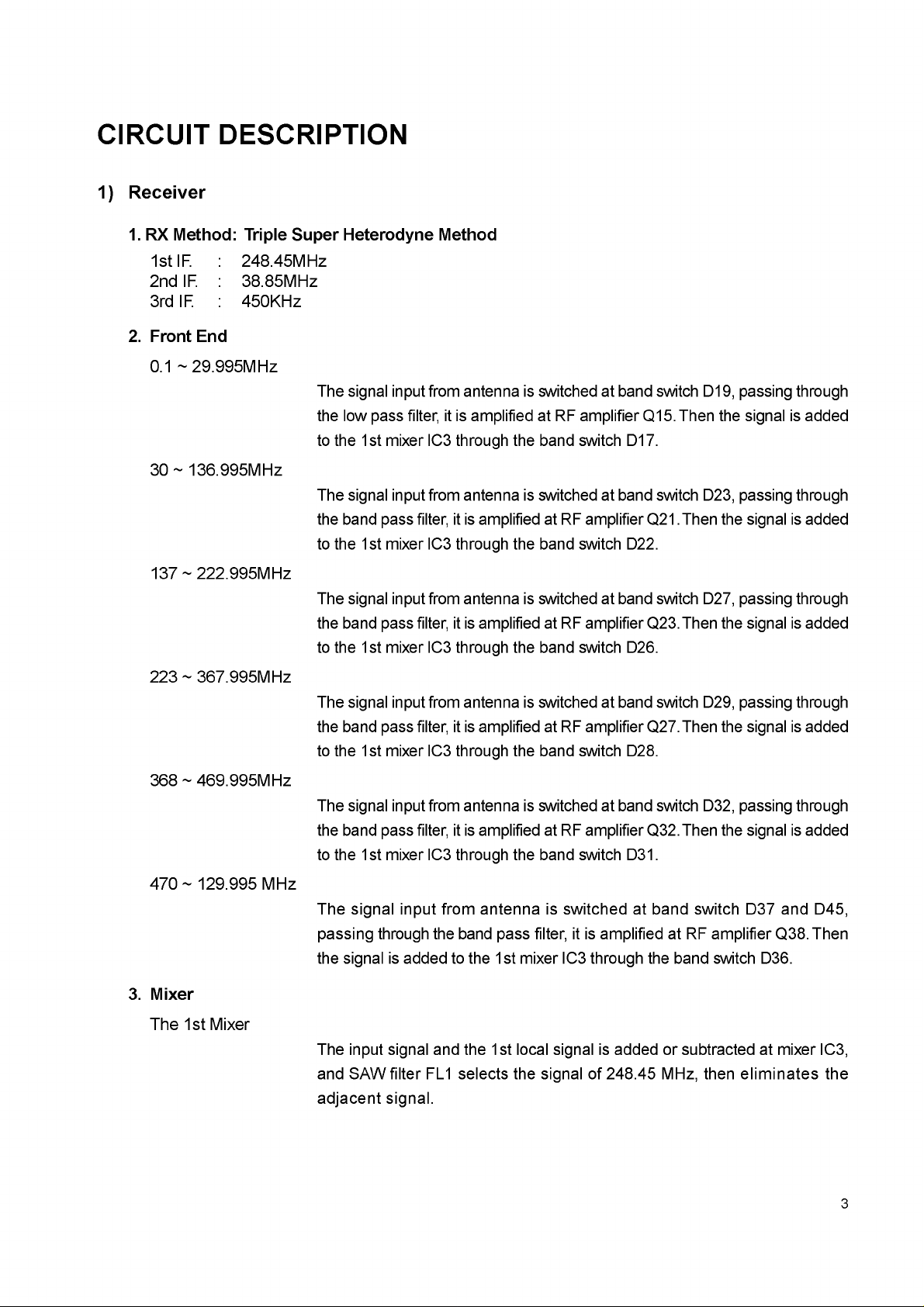
SPECIFICATIONS
1) GENERAL
Receiving range
Modulation mode
Ant. impedance
Ant. terminal
Supply voltage
Ground
Current consumption
Temperature range
Frequency stability
Dimension
Weight
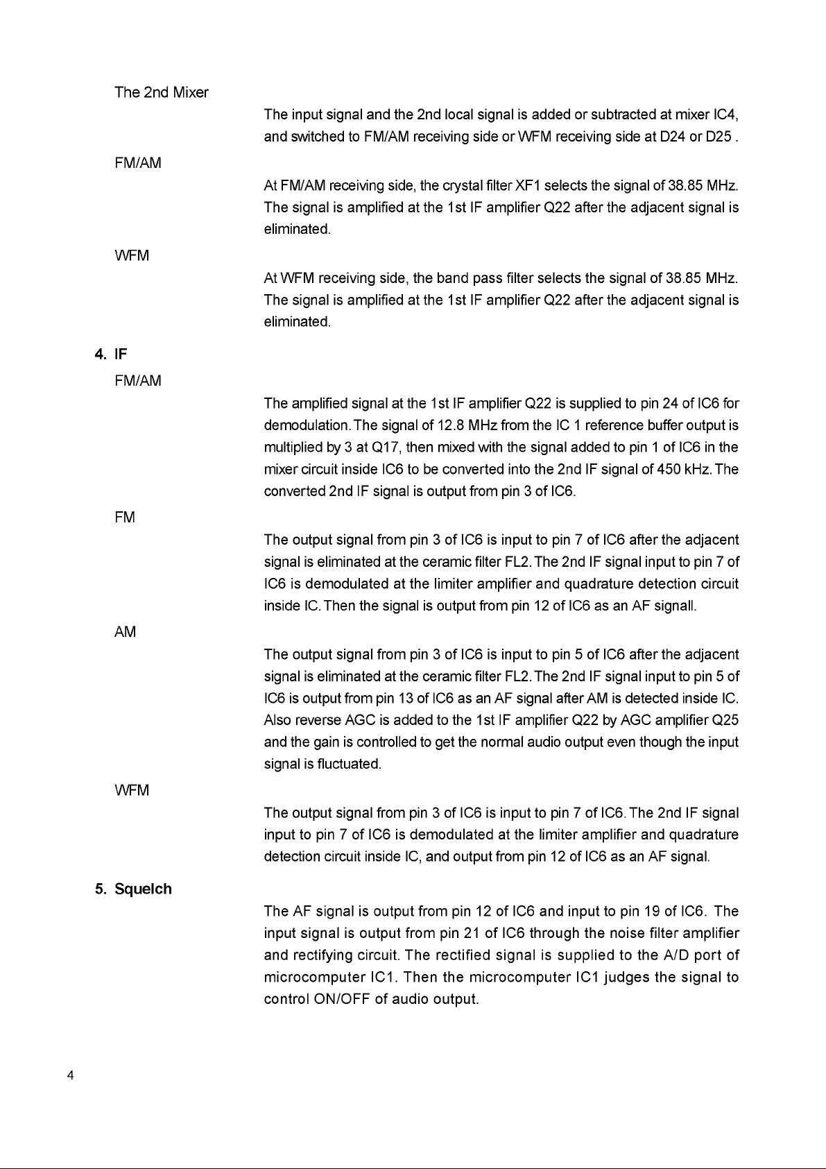
2) RECEIVER
System
First IF
Second IF
Third IF
Selectivity
Sensitivity
Typ.
Audio output power
E : 0.1 ~ 1299.995 MHz
T : 0.1 ~ 823.995 MHz
850.000 ~ 868.995 MHz
895.000 ~ 1299.995 MHz
FM, WFM, AM
50Q
SMA
DC 3.6V ~ 6V (Internal battery)
DC 4.5V ~ 16V (external regulated source)
Negative ground
reception : approx.75mA
Battery save (1:4)approx.39mA
-10 ~ +60°C (+14 ~ +140 F°)
±5ppm(-10 ~ +60°C)(+14 ~ +140F°)
56(W) x 102(H) x 23(D)mm
Approx.145g
Triple-conversion superheterodyne
248.45 MHz
38.85 MHz
450 kHz
AM/FM -6dB/12kHz or over , -60dB/30kHz or less
WFM -6dB/150kHz or over
FM/WFM 12dB SINAD, AM 10dB S/N
AM : 0.5 ~ 1.62MHz 17dBu 10dB S/N
1.625MHz or over 5dBu 10dB S/N
FM : 30 ~ 550MHz -3dBu 12dB SINAD
550MHz or over 0dBu 12dB SINAD
WFM : 76 ~ 770MHz 13dBu 12dB SINAD
more than 220mW (8Q)
2
Page 3
CIRCUIT DESCRIPTION
1) Receiver
1. RX Method: Triple Super Heterodyne Method
1st IF. : 248.45MHz
2nd IF. : 38.85MHz
3rd IF. : 450KHz
2. Front End
0.1 ~ 29.995MHz
The signal input from antenna is switched at band switch D19, passing through
the low pass filter, it is amplified at RF amplifier Q15. Then the signal is added
to the 1st mixer IC3 through the band switch D17.
30 ~ 136.995MHz
The signal input from antenna is switched at band switch D23, passing through
the band pass filter, it is amplified at RF amplifier Q21. Then the signal is added
to the 1st mixer IC3 through the band switch D22.
137 ~ 222.995MHz
The signal input from antenna is switched at band switch D27, passing through
the band pass filter, it is amplified at RF amplifier Q23. Then the signal is added
to the 1st mixer IC3 through the band switch D26.
223 ~ 367.995MHz
368 ~ 469.995MHz
470 ~ 129.995 MHz
3. Mixer
The 1st Mixer
The signal input from antenna is switched at band switch D29, passing through
the band pass filter, it is amplified at RF amplifier Q27. Then the signal is added
to the 1st mixer IC3 through the band switch D28.
The signal input from antenna is switched at band switch D32, passing through
the band pass filter, it is amplified at RF amplifier Q32. Then the signal is added
to the 1st mixer IC3 through the band switch D31.
The signal input from antenna is switched at band switch D37 and D45,
passing through the band pass filter, it is amplified at RF amplifier Q38. Then
the signal is added to the 1st mixer IC3 through the band switch D36.
The input signal and the 1st local signal is added or subtracted at mixer IC3,
and SAW filter FL1 selects the signal of 248.45 MHz, then eliminates the
adjacent signal.
3
Page 4
The 2nd Mixer
FM/AM
WFM
4. IF
FM/AM
The input signal and the 2nd local signal is added or subtracted at mixer IC4,
and switched to FM/AM receiving side or WFM receiving side at D24 or D25 .
At FM/AM receiving side, the crystal filter XF1 selects the signal of 38.85 MHz.
The signal is amplified at the 1st IF amplifier Q22 after the adjacent signal is
eliminated.
At WFM receiving side, the band pass filter selects the signal of 38.85 MHz.
The signal is amplified at the 1st IF amplifier Q22 after the adjacent signal is
eliminated.
The amplified signal at the 1st IF amplifier Q22 is supplied to pin 24 of IC6 for
demodulation. The signal of 12.8 MHz from the IC 1 reference buffer output is
multiplied by 3 at Q17, then mixed with the signal added to pin 1 of IC6 in the
mixer circuit inside IC6 to be converted into the 2nd IF signal of 450 kHz. The
converted 2nd IF signal is output from pin 3 of IC6.
FM
AM
WFM
5. Squelch
The output signal from pin 3 of IC6 is input to pin 7 of IC6 after the adjacent
signal is eliminated at the ceramic filter FL2. The 2nd IF signal input to pin 7 of
IC6 is demodulated at the limiter amplifier and quadrature detection circuit
inside IC. Then the signal is output from pin 12 of IC6 as an AF signall.
The output signal from pin 3 of IC6 is input to pin 5 of IC6 after the adjacent
signal is eliminated at the ceramic filter FL2. The 2nd IF signal input to pin 5 of
IC6 is output from pin 13 of IC6 as an AF signal after AM is detected inside IC.
Also reverse AGC is added to the 1st IF amplifier Q22 by AGC amplifier Q25
and the gain is controlled to get the normal audio output even though the input
signal is fluctuated.
The output signal from pin 3 of IC6 is input to pin 7 of IC6. The 2nd IF signal
input to pin 7 of IC6 is demodulated at the limiter amplifier and quadrature
detection circuit inside IC, and output from pin 12 of IC6 as an AF signal.
The AF signal is output from pin 12 of IC6 and input to pin 19 of IC6. The
input signal is output from pin 21 of IC6 through the noise filter amplifier
and rectifying circuit. The rectified signal is supplied to the A/D port of
microcomputer IC1. Then the microcomputer IC1 judges the signal to
control ON/OFF of audio output.
4
Page 5
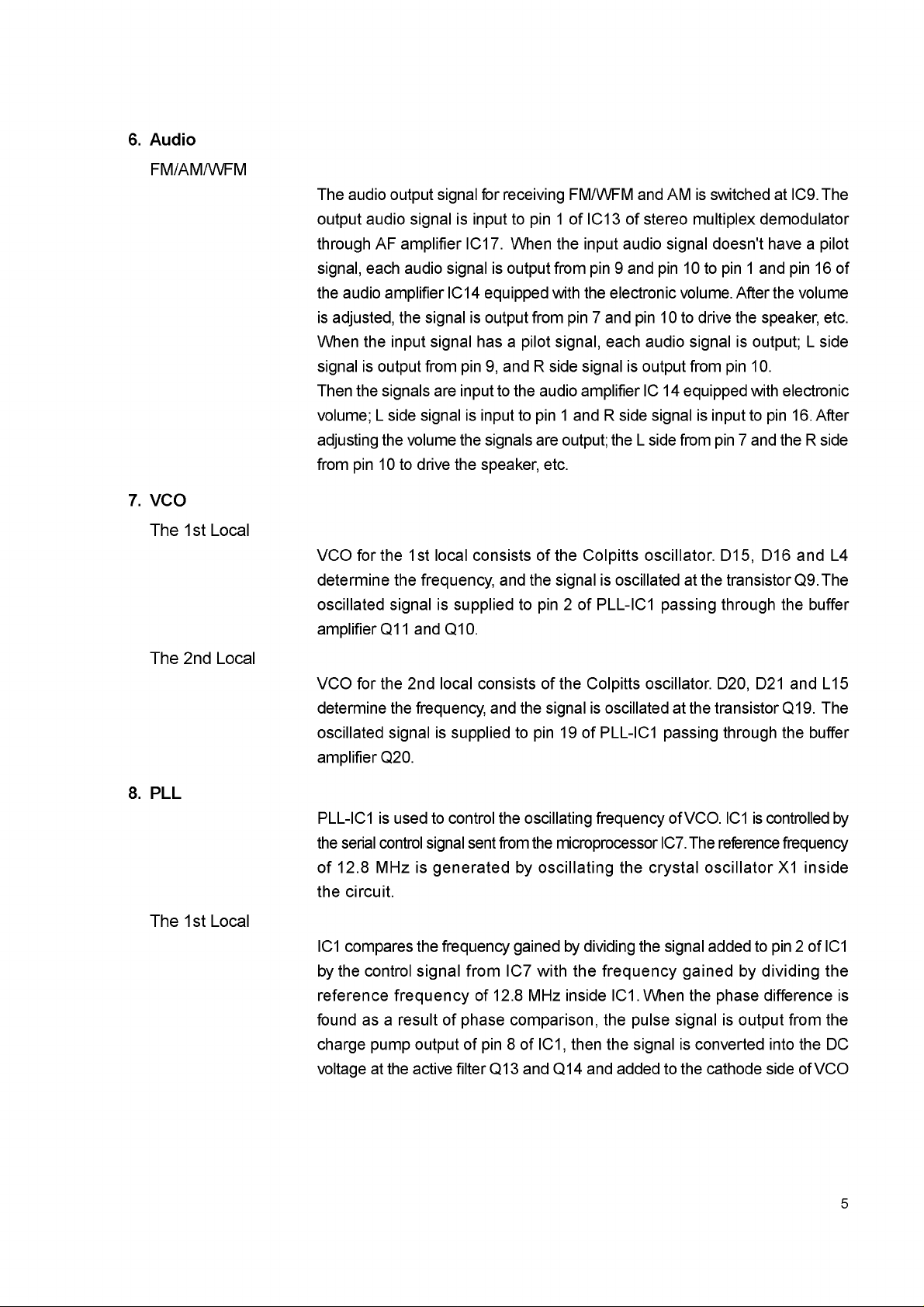
6. Audio
FM/AM/WFM
7. VCO
The 1st Local
The audio output signal for receiving FM/WFM and AM is switched at IC9. The
output audio signal is input to pin 1 of IC13 of stereo multiplex demodulator
through AF amplifier IC17. When the input audio signal doesn't have a pilot
signal, each audio signal is output from pin 9 and pin 10 to pin 1 and pin 16 of
the audio amplifier IC14 equipped with the electronic volume. After the volume
is adjusted, the signal is output from pin 7 and pin 10 to drive the speaker, etc.
When the input signal has a pilot signal, each audio signal is output; L side
signal is output from pin 9, and R side signal is output from pin 10.
Then the signals are input to the audio amplifier IC 14 equipped with electronic
volume; L side signal is input to pin 1 and R side signal is input to pin 16. After
adjusting the volume the signals are output; the L side from pin 7 and the R side
from pin 10 to drive the speaker, etc.
VCO for the 1st local consists of the Colpitts oscillator. D15, D16 and L4
determine the frequency, and the signal is oscillated at the transistor Q9. The
oscillated signal is supplied to pin 2 of PLL-IC1 passing through the buffer
amplifier Q11 and Q10.
The 2nd Local
8. PLL
The 1st Local
VCO for the 2nd local consists of the Colpitts oscillator. D20, D21 and L15
determine the frequency, and the signal is oscillated at the transistor Q19. The
oscillated signal is supplied to pin 19 of PLL-IC1 passing through the buffer
amplifier Q20.
PLL-IC1 is used to control the oscillating frequency of VCO. IC1 is controlled by
the serial control signal sent from the microprocessor IC7. The reference frequency
of 12.8 MHz is generated by oscillating the crystal oscillator X1 inside
the circuit.
IC1 compares the frequency gained by dividing the signal added to pin 2 of IC1
by the control signal from IC7 with the frequency gained by dividing the
reference frequency of 12.8 MHz inside IC1. When the phase difference is
found as a result of phase comparison, the pulse signal is output from the
charge pump output of pin 8 of IC1, then the signal is converted into the DC
voltage at the active filter Q13 and Q14 and added to the cathode side of VCO
5
Page 6

The 2nd Local
vari-cap D15 and D16 to make the phases equal. In result the stabilized
oscillation can be done at the desired frequency.
IC1 compares the frequency gained by dividing the signal added to pin 19 of
IC1 by the control signal from IC7 with the frequency gained by dividing the
reference frequency of 12.8 MHz inside IC1. When the phase difference is
found as a result of phase comparison, the pulse signal is output from the
charge pump output of pin 13 of IC1, then the signal is converted into the DC
voltage at the inside circuit for active filter and added to the cathode side of
VCO vari-cap D20 and D21 to make the phases equal. In result the stabilized
oscillation can be done at the desired frequency.
6
Page 7
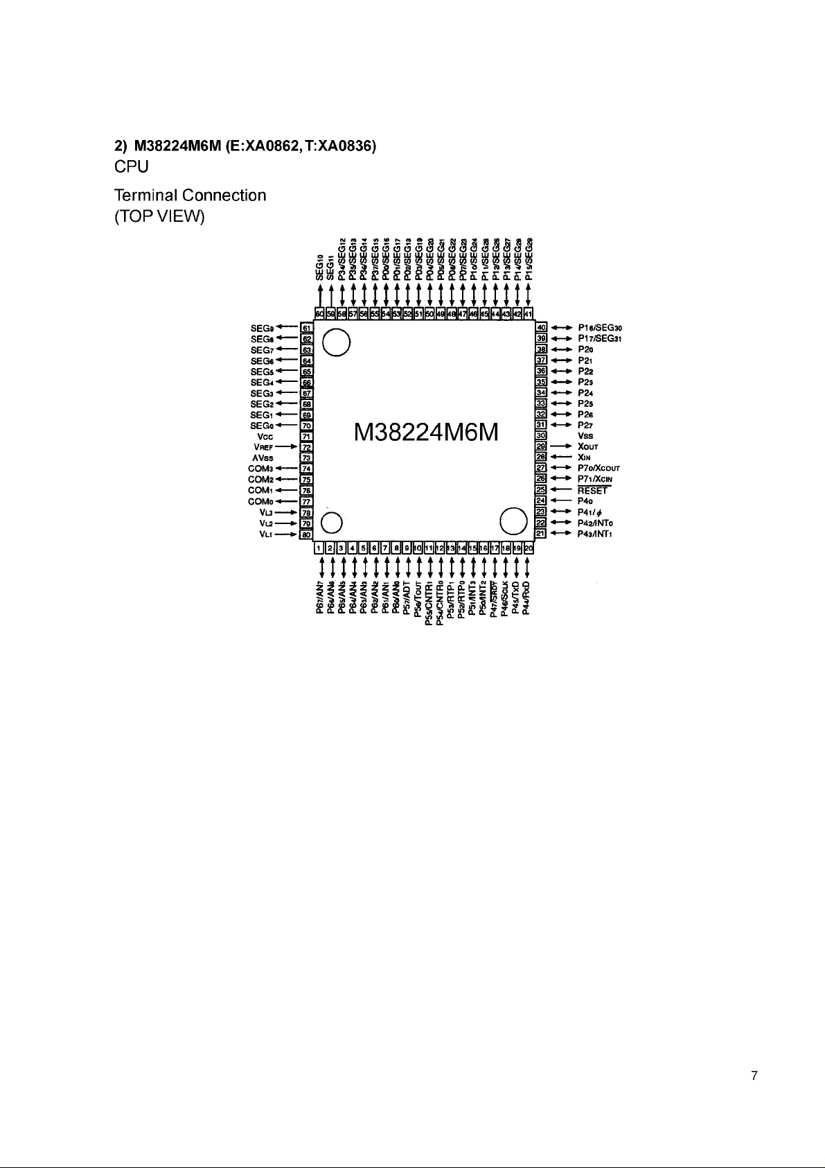
2) M38224M6M (E:XA0862, T:XA0836)
CPU
Terminal Connection
(TOP VIEW)
ssjssts-siiaaaa'aa&aa
000(900(300000000000
o »-LUUJUJlDLLILLJLULDLULULiJLUliJlULLIlULlJlU
nS!££££22 2££ £2ii£Eai
titilttiiiiiitiiilli
SEGs-
SEGs-
SEG?-
SEGe*
SEGs-
SEG4-
SE G3‘
SEG2*
SEGt-
SEGo-
Vco
Vhef-
AVss
COM3-
COM2 «
COM1-
COMo-
VL3-
Vl2 -
Vli -
■gear
o
M38224M6M
4c0 ■*—►
3g| •*—►
m ■*—* '
W + - +
36] -4—►
m ■*—►
m J ■*—►
32] -«— ►
ID -* —►
30)
1 1 — *-
10 •*—
w + - * >
m + —
¡ g * —
n * —
m ■«—►
13 <*—►
pi 6/segso
pi 7/SEG31
P2o
P21
P22
P23
P24
P25
P26
P27
Vss
XOUT
XlN
P7o/Xcout
P7i /Xcin
RESET
P4o
P4i/^
P42/INT0
P4s/INTi
m W M W M W t t
*&"»?> ^ ^
1 CD <D <0 <0 <0
CL Q l C L C L Q l
l il i
S & p
7
Page 8
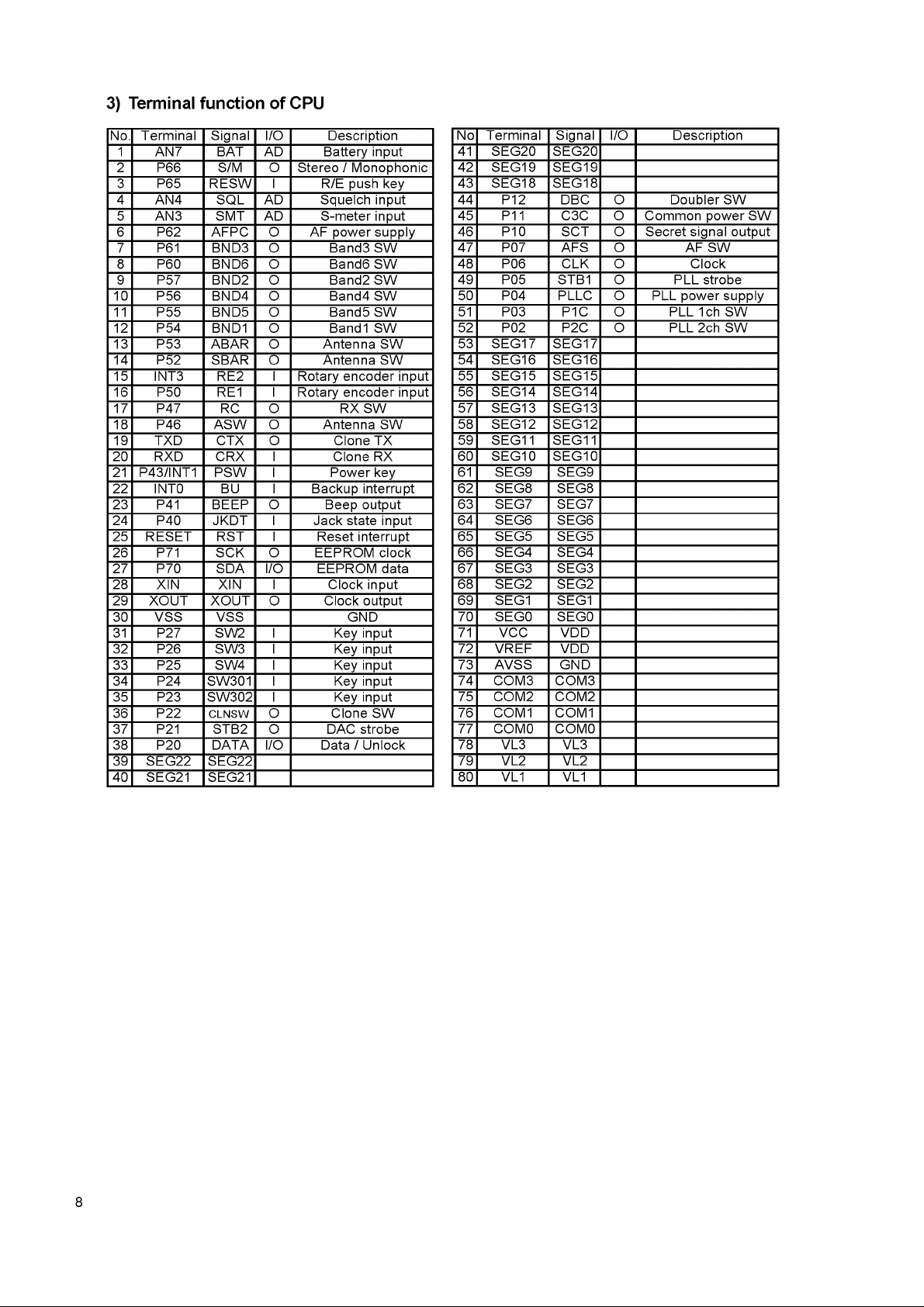
3) Terminal function of CPU
No. Term inal Signal I/O Description
1 AN7 BAT AD Battery input
2 P66 S/M O Stereo / Monophonic
3 P65 RESW I R/E push key
4 AN4 SQ L AD Squelch input
5 AN3 SMT AD S-meter input
6 P62 AFPC O AF power supply
7 P61 BND3 O Band3 SW
8 P60 BN D6 O Band6 SW
9 P57 BND2 O Band2 SW
10 P56 BND4 O Band4 SW
11 P55 BND5 O Band5 SW
12 P54 BND1 O Band1 SW
13 P53 ABAR O Antenna SW
14 P52 SBAR O Antenna SW
15 INT3 RE2 I Rotary encoder input
16 P50 RE1 I Rotary encoder input
17 P47 RC O RX SW
18 P46 AS W O Antenna SW
19 TXD CTX O Clone TX
20 RXD CRX I Clone RX
21 P43/INT1 P SW I Power key
22 INT0 BU I Backup interrupt
23 P41 BEEP O Beep output
24 P40 JKD T I Jack state input
25 RESET RST I Reset interrupt
26 P71 SCK O EEPROM clock
27 P70 SDA I/O EEPROM data
28 XIN XIN I Clock input
29 XOUT XO UT O Clock output
30 VSS VSS GND
31 P27 SW2 I Key input
32 P26 SW3 I Key input
33 P25 SW4 I Key input
34 P24 SW301 I Key input
35 P23 SW302 I Key input
36 P22 CLNSW O Clone SW
37 P21 STB2 O DAC strobe
38 P20 DATA I/O Data / Unlock
39 SEG22 SEG22
40 SEG21 SEG21
No Terminal Signal I/O Description
41 SEG20 SEG20
42 SEG19 SEG19
43 SEG18 SEG18
44 P12 DBC O Doubler SW
45 P11 C3C O Com mon power SW
46 P10 SCT O Secret signal output
47 P07 AFS O AF SW
48 P06 CLK O Clock
49 P05 STB1 O PLL strobe
50 P04 PLLC O PLL power supply
51 P03 P1C O PLL 1ch SW
52 P02 P2C O PLL 2ch SW
53 SEG17 SEG17
54 SEG16 SEG16
55 SEG15 SEG15
56 SEG14 SEG14
57 SEG13 SEG13
58 SEG12 SEG12
59 SEG11 SEG11
60 SEG10 SEG10
61 SEG9 SEG9
62 SEG8 SE G8
63 SEG7 SEG7
64 SEG 6 SEG 6
65 SEG5 SEG5
66 SEG4 SEG4
67 SEG3 SEG3
68 SEG2 SEG2
69 SEG1 SEG1
70 SEG0 SEG0
71 VCC VDD
72 VREF VDD
73 AVSS GND
74 COM3 COM3
75 COM2 COM2
76 COM1 COM1
77 COM0 COM0
78 VL3 VL3
79 VL2 VL2
80 VL1 VL1
8
Page 9
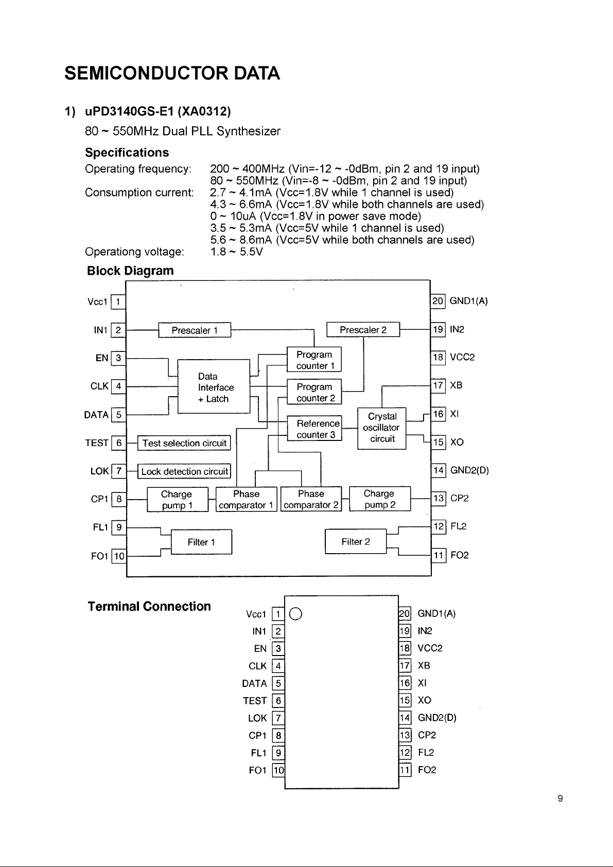
SEMICONDUCTOR DATA
1) uPD3140GS-E1 (XA0312)
80 ~ 550MHz Dual PLL Synthesizer
Specifications
Operating frequency:
Consumption current
Operationg voltage:
Block Diagram
200 ~ 400MHz (Vin=-12 ~ -0dBm, pin 2 and 19 input)
80 ~ 550MHz (Vin=-8 ~ -0dBm, pin 2 and 19 input)
2.7 ~ 4.1mA (Vcc=1.8V while 1 channel is used)
4.3 ~ 6.6mA (Vcc=1.8V while both channels are used)
0 ~ 10uA (Vcc=1.8V in power save mode)
3.5 ~ 5.3mA (Vcc=5V while 1 channel is used)
5.6 ~ 8.6mA (Vcc=5V while both channels are used)
1.8 ~ 5.5V
Vcc1 1
IN1 2
EN
CLK
DATA
TEST l~6
LOK 7
CP1
FL1
F01 10
4
Test selection circuit
Lock detection circuit
Charge
pump 1
_n
Prescaler 1
Data
Interface
+ Latch
Filter 1
Phase Phase
comparator 1
comparator 2
Program
counter 1
Program
counter 2
Reference
counter 3
Prescaler 2
Crystal
oscillator
circuit
Charge
pump 2
Filter 2
20 G ND1(A)
19 IN2
VCC2
18
XB
17
XI
16
15 XO
14 GND2(D)
CP2
13
FL2
12
11 F 0 2
Terminal Connection
Vcc1
[ I
IN1 [IF
EN 3
CLK 4
DATA 5
TEST 6
LOK 7
CP1
FL1 9
F01 10
GND1(A)
o
8
20
19 IN2
VCC2
18
17 XB
16 XI
15 XO
GND2(D)
14
CP2
13
12 FL2
11 F02
9
Page 10
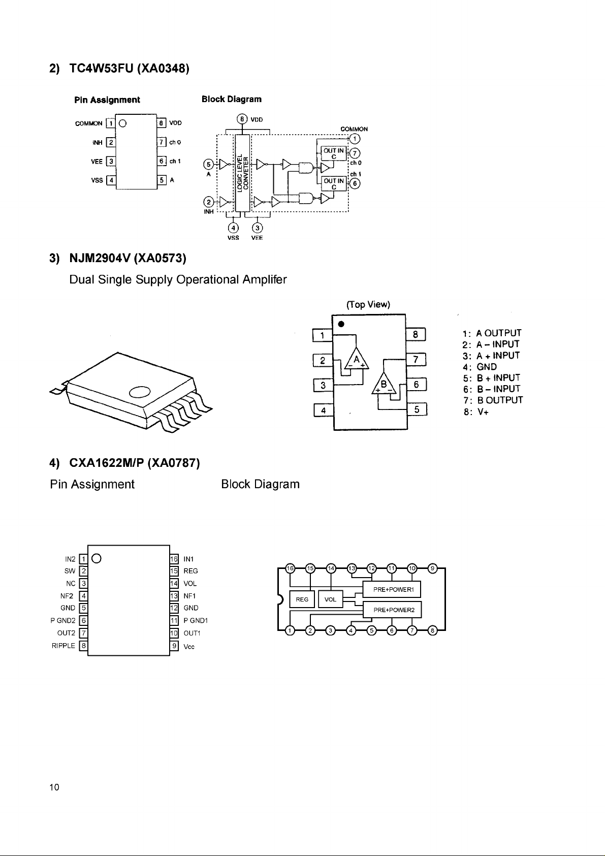
2) TC4W53FU (XA0348)
Pin Assignment
COMMON [T
O
T| VOD
Block Diagram
L-.
(NH (T
VEE [T
VSS ( T 7] A
~7~| ch 0
~6~] ch 1
®it>4
A ; ;
(Dtj>H
INH
88
VSS VEE
3) NJM2904V (XA0573)
Dual Single Supply Operational Amplifer
? ) VDD
' Ljoui ’’
: \ c
' i' '
.......................
COMMON
OUT IN
OUT IN | 0
(Top View)
1: A OUTPUT
2: A -IN PU T
3: A + INPUT
4: GND
5: B +INPU T
6: B-IN PU T
7: BOUTPUT
8: V+
4) CXA1622M/P (XA0787)
Pin Assignment
IN2 [T
o
sw [2
NC [3
NF2 [4
GND [5
P GND2 [6
OUT2 [7
RIPPLE [8
Block Diagram
10
Page 11
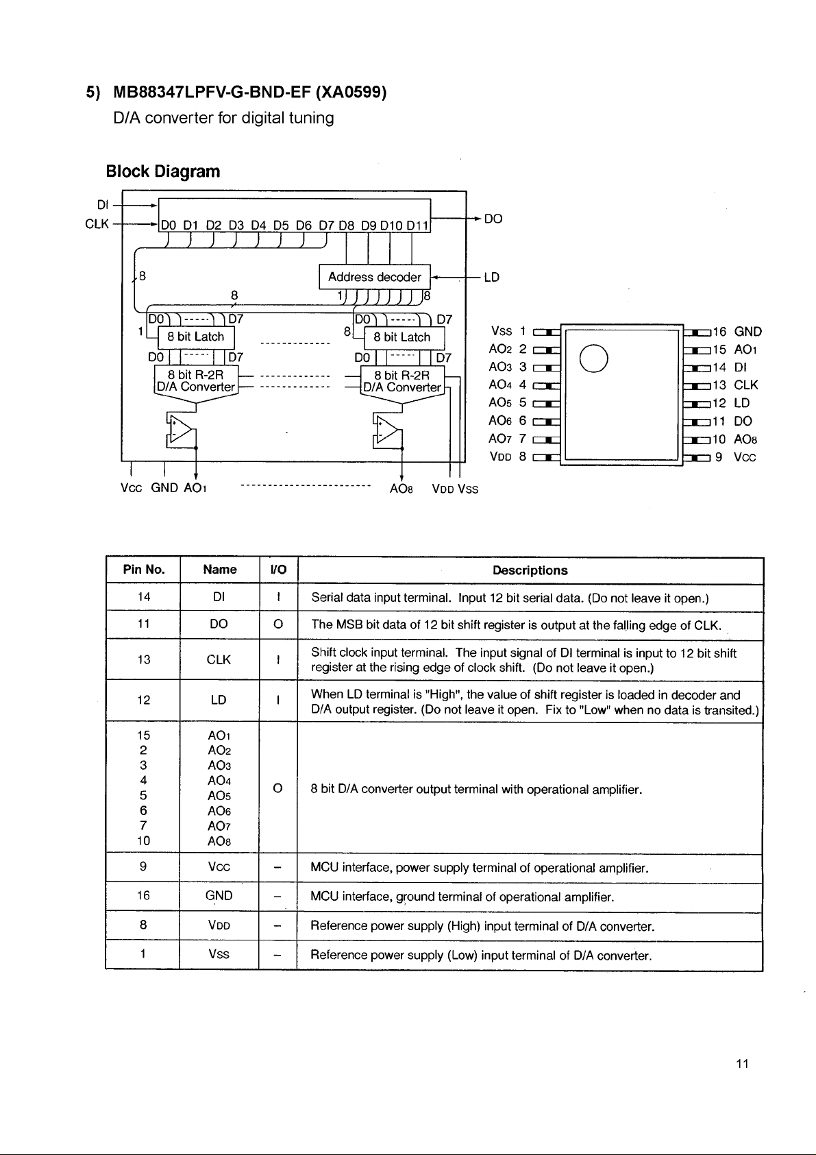
5) MB88347LPFV-G-BND-EF (XA0599)
D/A converter for digital tuning
Block Diagram
Dl
CLK •
DO D1 D2 D3 D4 D5 D6 D7 D8 D 9D 10D 11
i m r m
-DO
8
D P I 1
.........
1 1 0 7
— 8 bit Latch
Vcc GND A 0 i
Pin No. Name
14 Dl I
11
13
DO
CLK I
Address decoder
LD
'J J J J J J J J° '
p p n
.........
i ~ iD 7
— 8 bit Latch
AOs V dd V ss
I/O
Serial data input terminal. Input 12 bit serial data. (Do not leave it open.)
o
The MSB bit data of 12 bit shift register is output at the falling edge of CLK.
Shift clock input terminal. The input signal of Dl terminal is input to 12 bit shift
register at the rising edge of clock shift. (Do not leave it open.)
1
vss
r i '
A02 2
<
<
AOs 5 r m
<
A07 7
o
CO
o
o
to
<oO
i ■—
r-m -
3
4
r~r~
r " i
6
r ■
8 r ■
Descriptions
GND
1tt
15 AOi
14 Dl
CLK
13
12 LD
11
DO
10 AOs
9 Vcc
12 LD I
15
2
3
4
5
6
7
10
9
16 GND
8
1
> > > > > > > >
Vcc
V dd
Vss
o o o o o o o o
When LD terminal is "High", the value of shift register is loaded in decoder and
D/A output register. (Do not leave it open. Fix to "Low" when no data is transited.)
0
8 bit D/A converter output terminal with operational amplifier.
-
MCU interface, power supply terminal of operational amplifier.
-
MCU interface, ground terminal of operational amplifier.
-
Reference power supply (High) input terminal of D/A converter.
-
Reference power supply (Low) input terminal of D/A converter.
11
Page 12
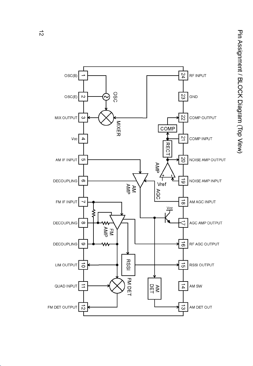
OSC(B)
OSC(E)
Pin Assignment / BLOCK Diagram (Top V iew )
MIX OUTPUT
AM IF INPUT
DECOUPLING
FM IF INPUT
DECOUPLING
DECOUPLING
LIM OUTPUT
QUAD INPUT
COMP OUTPUT
COMP INPUT
NOISE AMP OUTPUT
05
\ /
> v \ /
>
t T t
1
Vref
>
CD
O
■ O ,
NOISE AMP INPUT
5
AM AGC INPUT
AGC AMP OUTPUT
“0
-\W — "
XJ
V )
V )
RF AGC OUTPUT
RSSI OUTPUT
FM DET OUTPUT
AM DET OUT
Page 13

7) TK10931V (XA0666)
CD T)
O
O
7T
O
0)'
(Q
3
3
O
C/3
O
O
7s
O
7s
6) TK11816M (XA0665)
u '
>
(/)
(/)
cq '
=3
3
(D
O
7s
Page 14

8) TA4101F TE12L (XA0667)
Pin Assignment
8 7 6 5
n n n n
u u u u
1 2 3 4
1. IF OUT 5. BASE
2. Vcc 6. BASE
3. O S C IN 7. G ND
4. BASE 8. COLLEC TOR
9) S-80828ALNP-EAR-T2 (XA0834)
Pin Assignment
4
Top view
Block Diagram
R2 S RB3
HVW
3
1 O UT
8
1
4
6
7
3
Block Diagram
2 Vdd
3 NC
4 Vss
13
Page 15

10) BR24C64F-E2 (XA0669)
Block Diagram
AO i
Ai 2
A2 3
GND 4
4
Pin Assignment
"fiSb it
ADDRESS
DECODER
CO NTROL C IR CUIT
I
HIGH VOLTAGE
GENERATOR
Vcc WP SCL SDA
64Kbit EEP ROM ARR AY
h
iSbit
SLAVE^WORD
ADDRESS REGISTER
\
START STOP
VOLTAGE
DETECTOR
ACK
DATA
REGISTER
H
r
8 Vcc
7 WP
6 SCL
5
5 SDA
o
11 ) S-B1230SG-QB-X (XA0B33)
Pin Assignment
BR24C64/F
AO Ai A2 GND
Block Diagram
GN D V in V a n
i4
Page 16

12) uPC2757T-E3 (XA0743)
Terminal Connection
(Top View) (Bottom View)
3 □
2 H
1 H
Block Diagram
X
r >
□ 4 4 H
□ 5 5 1!
O
1: R F input 4: PS (Power Save)
2: GND 5: Vcc
3: Lo input 6: IF output
□ 6 6 H
O
3
2
1
input
13) TC7SET08FU (XA0586)
Pin Assignment Block Diagram
IN B
1
IN A
G 2
GND23
5 Vcc
4
OUT Y
15
Page 17

14)LA3335M (XA0786)
Pin Assignment
10
9 6
O
5 1
2
1: Input
2: PLL loop filter
3: Power supply
4: VCO
5: NC
Block Diagram
6 : GN D
7 : Stereo indicator fillter
8 : Pilot sync detection
9 : Decoder output (low)
10 : Decoder output (high)
16
Page 18

15) NJM2107 (XA0B50)
Pin As s ig nm en t
{T op V ie w ) i _ 4 -IN P U T
1 5
Z
3 i
^ 3 , - IN P U T
Z 2
Z . V "
4 , O rT T Ü T
5 , V H-
1e) Transistor, Diode and LED Outline Drawings
1SVS08(fPHS)
"xD0s"S9" '
SML-S10MTT86
""XLO0"S6
......
- i
2SK881Y(TE85R)
......
x'E0036.........
s
K Y
UMC5N TR
"""xU0Í52"'
DAN2S5E-TL
""xDöS2ö""
=£=
2SC47S8BL(TE85R)
......
x T0í 8í
........
1=1 1=1 1=1
L L M 2 Y R V Y
UN911H Tx
"xU0092
c
6 R
x p ii i i-tx
""xU0i7'i"'
MA2SS57-Tx
" "x D0SS'7""
p l .
N
"
2SC5066FT-Y(TE85L)
......
xfölaö.........
DTC14STE TL
"'"xU 0Í96" "
C
O 3
ISSS90 TE61
xDöS42
Ï [
2SD2216R-Tx
" " xt Oí SS
.
x P01501
"xU0i72"
5 R
Id y Id
B E B
......
MA2SS0400L
x DOSÍ2
......
f t f t
2SJ144Y(TE85R)
......
xEboÍ9""""
n
2SK1580
" xeöö29"
D
G1S
MA2S728-Tx
""xD0's'i5""
i
MA2Z720
"xDöS6"7"
Ä
2L
ISSS62 TE85L
'""xDöSS8
i :
CS
2SB11S2T
""xfo06Í"""
B A
ü bd ü
B C E
......
17
Page 19

17) LCD connection
Pin No COMO COM1 COM2 COM3
1 COMO - - -
2 - COM1 - -
3 - - COM2 -
4 - - - COM3
5 D E F
6 H I
7 L M N K
8 P
9 R
10 9c 9b 9a Y
11 9e
12 8c 8b 8a X
13 8e
14 7c 7b 7a Z
15 7e
16 6c 6b 6a 6h
17 6e
18 5c 5b 5a
19 5e
20 4c 4b 4a 4h
21 4e
22 3c 3b 3a B2
23 3e
24 2c 2b 2a B1
25 2e
26 1c 1b 1a A
27 1e
O
S U
9g
8g
7g
6g
5g
4g
3g
2g
1
g
J G
V W
9f 9d
8f 8d
7f 7d
6f 6d
5f 5d
4f 4d
3f 3d
2f 2d
1f 1d
C
T
Q
18
Page 20

EXPLODED VIEW
1) Front View
UR0023
19
Page 21

2) Bottom View
AX0005
AN0027
NK0077
VSP0013
'AN0012
20
Page 22

PARTS LIST
MAIN Unit
Parts No. Descriptin Parts Name
Ref.No.
C1 CU3111 Chip C. C 1608JB1C104KT-N
C2 CU3111 Chip C. C1608JB1C104KT-N
C3 CU3111 Chip C. C1608JB1C104KT-N
C4 CU3111 Chip C. C1608JB1C104KT-N
C5 CU3111 Chip C. C1608JB1C104KT-N
C6 CU3535 Chip C. GRM 36B102K50PT
C7 CU3535 C hip C. GRM36B102K50PT
C8 CU3535 Chip C. GRM 36B102K50PT
C9 CU3535 C hip C. GRM36B102K50PT
C10 CU3535 Chip C. GR M36B102K50PT
C11 C U3535 Chip C. GRM 36B102K50PT
C12 CU3111 Chip C. C1608JB1C104KT-N
C13 CS0395 Chip Tantal TMCMB0G686MTR
C14 CS0418 Chip Tantal TMCMC1C476MTR
C15 CU3506 Chip C. GRM 36C H050C50PT
C16 CU3547 Chip C. G RM36B103K 16PT
C17 CU3535 Chip C. G RM36B102K 50PT
C18 CS0411 Chip Tantal 4MCM 226MATER
C19 CU3111 Chip C. C1608JB1C104KT-N
C20 CU3512 Chip C. G RM36CH120J50PT
C21 CU3511 Chip C. G RM 36CH 100D50PT
C22 CU3518 Chip C. G RM36CH390J50PT
C23 CU3523 Chip C. G RM36CH101J50PT
C24 CS0397 Chip Tantal TMCP1C 105MTR
C25 CS0395
C26 CS0396 Chip Tantal TMCP1D 104MTR
C27 CU3535 Chip C. G RM36B102K 50PT
C28 CU3547 Chip C. G RM36B103K 16PT
C29 CU3501 Chip C. G RM36CK0R5C50PT
C30 CU3535 Chip C. G RM36B102K 50PT
C31 CU3111 Chip C. C1608JB1C104KT-N
C32 CS0397 Chip Tantal TMCP1C 105MTR
C33 CS0411 Chip Tantal 4MCM 226MATER
C34 CU3523 Chip C. G RM36CH101J50PT
C35 CU3535 Chip C. G RM36B102K 50PT
C36 CU3535 Chip C. G RM36B102K 50PT
C37 CS0396 Chip Tantal TMCP1D 104MTR
C38 CU3535 Chip C. G RM36B102K 50PT
C39 CU3547 Chip C. G RM36B103K 16PT
C40 CU3111 Chip C. C1608JB1C104KT-N
C41 CU3111 Chip C. C1608JB1C104KT-N
C42 CS0397 Chip Tantal TMCP1C 105MTR
C43 CU3111 Chip C. C1608JB1C104KT-N
C44 CU3111 Chip C. C1608JB1C104KT-N
C45 CU3547 Chip C. G RM36B103K 16PT
C46 CU3515 Chip C. G RM36CH220J50PT
C47 CU3547 Chip C. G RM36B103K 16PT
C48 CU3111 Chip C. C1608JB1C104KT-N
C49 CU3503 Chip C. GRM 36C K020C50PT
C50 CU3503 Chip C. GRM 36C K020C50PT
C51 C U3503 Chip C. GRM 36CK020C50PT
C52 CU3535 Chip C. G RM36B102K 50PT
C53 CU3111 Chip C. C1608JB1C104KT-N
Chip Tantal
TMCMB0G686MTR
Ver
Ref.No. Parts No. Descriptin Parts Name Ver
C54 CU3503 Chip C. GRM 36C K020C50PT
C55 CS0397
C56 CU3515 Chip C. GR M36C H220J50PT
C57 CS0403 Chip Tantal TMCP1D224MTR
C58 CU3523 Chip C. GR M36C H101J50PT
C59 CU3527 Chip C. GR M36C H221J25PT
C60 CU3527 Chip C. GR M36C H221J25PT
C61 C U3523 Chip C. GRM36CH101J50PT
C62 CU3535 Chip C. GR M36B102K50PT
C63 CS0411 Chip Tantal 4M CM 226MATER
C64 CU3503 Chip C. GRM 36C K020C50PT
C65 CU3535 Chip C. GR M36B102K50PT
C66 CU3515 Chip C. GRM36CH 220J50PT
C67 CU3535 Chip C. GR M36B102K50PT
C68 CU3547 Chip C. GRM 36B103K16PT
C69 CU3111 Chip C. C1608JB1C104KT-N
C70 CU3535 Chip C. GR M36B102K50PT
C71 C U3527 Chip C. GRM36CH221J25PT
C72 CU3514 Chip C. GR M36C H180J50PT
C73 CU3510 Chip C. GRM 36C H090D50PT
C74 CS0395 Chip Tantal TMCM B0G 686MTR
C75 CU3504 Chip C. GR M36CJ030C50PT
C76 CU3551 Chip C. G RM36B223K16PT
C77 CS0397 Chip Tantal TM CP1C105MTR
C78 CU3527 Chip C. GR M36CH221J25PT
C79 CU3547 Chip C. GR M36B103K16PT
C80 CU3535 Chip C. GR M36B102K50PT
C81 CS0412 Chip Tantal 16MCM 156MB2TER
C82 CU3547 Chip C. GR M36B103K16PT
C83 CU3521 Chip C. G RM36CH680J50PT
C84 CU3521 Chip C. G RM36CH680J50PT
C85 CU3516 Chip C. GR M36CH270J50PT
C86 CU3547 Chip C. GRM 36B103K16PT
C87 CU3517 Chip C. GR M36CH330J50PT
C88 CU3520 Chip C. GRM 36CH560J50PT
C89 CU3517 Chip C. GR M36CH330J50PT
C90 CU3547 Chip C. GR M36B103K16PT
C91 CU3547 Chip C. GR M36B103K16PT
C92 CU3547 Chip C. GR M36B103K16PT
C93 CU3547 Chip C. GR M36B103K16PT
C94 CU3505 Chip C. GR M36C H040C50PT
C95 CU3547 Chip C. GR M36B103K16PT
C96 CU3547 Chip C. GR M36B103K16PT
C97 CU3111 Chip C. C 1608JB1C104KT-N
C98 CU3513 Chip C. GR M36CH150J50PT
C99 CU3509 Chip C. GR M36C H080D50PT
C100 CU3111 Chip C. C1608JB1C 104KT-N
C101 CU3535 Chip C. GRM 36B102K50PT
C102 CS0378 Chip Tantal TMCM C0G107M TR
C103 CU3535 Chip C. GRM 36B102K50PT
C104 CU3535 Chip C. GRM 36B102K50PT
C105 CU3512 Chip C. GRM 36CH 120J50PT
C106 CU3535 Chip C. GRM 36B102K50PT
Chip Tantal
TMCP1C105MTR
21
Page 23

Parts No. Descriptin Parts Name
Ref.No.
C107 CU3502 Chip C. GRM36CK010C50PT
C10B CU3509 Chip C. GRM36CH0B0D50PT
C109 CU3509 Chip C. GRM36CH0B0D50PT
C110 CU351B Chip C. GRM 36CH390J50PT
C111 CU3535 Chip C. GRM36B102K50PT
C112 CU3516 Chip C. GRM 36CH 270J50PT
CU3520 Chip C. G RM36CH560J50PT
C113
C114 CU3516 Chip C. GRM 36CH 270J50PT
C115 CU3551 Chip C. G RM36B223K 16PT
C116 CS040B Chip Tantal 6MCM156MATER
C117
CU3111
C11B CU3535 Chip C. GR M36B102K50PT
C119 CU3515 Chip C. GRM 36CH 220J50PT
C120 CU3506 Chip C. GRM36CH050C50PT
C121 CU3506 Chip C. GRM 36CH050C50PT
C122 CU351B Chip C. GRM 36CH390J50PT
C123 CU3551 Chip C. G RM36B223K 16PT
C124 CU3523 Chip C. GRM 36CH 101J50PT
C125 CU3523 Chip C. GRM 36CH 101J50PT
C126 CU3551 Chip C. G RM36B223K 16PT
C127 CU3535 Chip C. GRM 36B102K50PT
C12B CU3551 Chip C. GR M36B223K16PT
C129 CU3535 Chip C. GRM 36B102K50PT
C130 CS0404 Chip Tantal 6MCM 106MATER
CU3535 Chip C. G RM36B102K50PT
C131
C132 CU3514 Chip C. GRM36CH1B0J50PT
C133 CU3517 Chip C. GRM 36CH 330J50PT
C134 CU3514 Chip C. GRM36CH1B0J50PT
C135 CU3535 Chip C. GRM 36B102K50PT
C136 CU3535 Chip C. GRM 36B102K50PT
C137
CU3111
C13B CS040B Chip Tantal 6MCM 156MATE R
C139 CU3531 Chip C. G RM36B471K 50PT
C140
CU3111
C141 CU3511 Chip C. GRM36C H100D50PT
C142 CU3547 Chip C. GRM 36B103K16PT
C143
CU3111
C144
CU3111
C145
CU3111
C146 CU3535 Chip C. GRM36B 102K50PT
C147 CS040B
C14B CU3531 Chip C. G RM 36B471K50PT
C150 CS0411
C151 CU3531 Chip C. G RM36B471K50PT
C152 CU3535 Chip C. GRM36B 102K50PT
C153 CU3511 Chip C. GRM 36CH 100D50PT
C154 CU3503 Chip C. GRM 36CK020C50PT
C155 CU3503 Chip C. GRM 36CK020C50PT
C156 CU3535 Chip C. GRM36B 102K50PT
C157 CU3547 Chip C. GRM36B 103K16PT
C15B CU3547 Chip C. GR M36B103K16PT
C159 CU3547 Chip C. GRM36B 103K16PT
C160 CU3547 Chip C. GRM36B 103K16PT
C161 CU3547 Chip C. GR M36B103K16PT
C162 CU3535 Chip C. GRM36B 102K50PT
C163 CS040B Chip Tantal 6MC M156M ATER
C164 CU3513 Chip C. GRM36C H150J50PT
C165 CU3517 Chip C. GRM36C H330J50PT
C166 CU3515 Chip C. GRM36C H220J50PT
C167
CU3111
C16B CS0396 Chip Tantal TM CP1D104MTR
Chip C. C160BJB1C104KT-N
Chip C. C160BJB1C104KT-N
Chip C. C160BJB1C104KT-N
Chip C. C160BJB1C104KT-N
Chip C. C160BJB1C104KT-N
Chip C. C160BJB1C104KT-N
Chip Tantal
Chip Tantal
Chip C. C160BJB1C104KT-N
6MCM156MATER
4MCM226MATER
Ver
Ref.No. Parts No. Descriptin Parts Name Ver
C169
CU3111
C170
CU3111
C171 CU3517 Chip C. GRM36C H330J50PT
C172 CU3517 Chip C. GRM 36CH 330J50PT
C173
CU3111
C174 CS039B Chip Tantal TMCP0J225MTR
C175 CS039B Chip Tantal TMCP0J225MTR
C176
CU3111
C177
CU3111
C17B CU3547 Chip C. GRM 36B103K16PT
C179 CU3513 Chip C. GRM 36CH 150J50PT
C1B0 CU3531 Chip C. GR M36B471K50PT
C1B1 CS041B Chip Tantal TMC MC1C476M TR
C1B2
CU3111
C1B3 CU3531 Chip C. GR M36B471K50PT
C1B4
CU3111
C1B5 CU3535 Chip C. GRM 36B102K50PT
C1B6 CU3535 Chip C. GRM 36B102K50PT
C1B7 CU3531 Chip C. GR M36B471K50PT
C1BB CU3507 Chip C. GRM36CH060D50PT
C1B9 CU3504 Chip C. GRM 36CJ030C50PT
C190 CU3504 Chip C. GRM 36CJ030C50PT
C191 CU3509 Chip C. GRM36CH0B0D50PT
C192 CU010B Chip C. LMK212BJ105K G
C193
CU3111
C194 CU3503 Chip C. GRM36CK020C50PT
C195 CS0395 Chip Tantal TMCMB0G6B6MTR
C196
CU3111
C197 CU351B Chip C. GRM 36CH390J50PT
C19B CU3535 Chip C. GRM 36B102K50PT
C199 CS0411 Chip Tantal 4MC M226M ATER
C200 CS0395 Chip Tantal TMCMB0G6B6MTR
C201 CU3547 Chip C. GRM36B103K16PT
C202 CU3547 Chip C. GRM 36B103K16PT
C203 CU010B Chip C. LMK212BJ105K G
C204 CS039B Chip Tantal TMCP0J225MTR
C205 CU010B Chip C. LMK212BJ105K G
C206 CU3551 Chip C. G RM36B223K 16PT
C207 CU3551 Chip C. G RM36B223K 16PT
C20B CS0397 Chip Tantal TMCP1C105MTR
C209
CU3111
C210
CU3111
C211
CU3111
C212 CS039B Chip Tantal TMCP0J225MTR
C213 CS0395 Chip Tantal TMCMB0G6B6MTR
C214
CU3111
C215 CU3523 Chip C. GRM 36CH 101J50PT
C216 CU3545 Chip C. GRM36B6B2K25PT
C217 CU3545 Chip C. GRM36B6B2K25PT
C21B CU3027 Chip C. C160BCH1H221JT-AS
C219 CU3535 Chip C. GRM 36B102K50PT
C220 CU3551 Chip C. G RM36B223K 16PT
D1 XD0339 Diode 1SV30B(TPH3)
D2 XD0342 Diode 1SS390TE61
D3 XD0342 Diode 1SS390TE61
D4 XD0342 Diode 1SS390TE61
D5 XD0342 Diode 1SS390TE61
D6 XD0342 Diode 1SS 390TE61
D7 XD033B Diode 1SS362(TEB5L)
DB XD0339 Diode 1SV30B(TPH3)
D9 XD0367 Diode MA2Z720
Chip C. C160BJB1C104KT-N
Chip C. C160BJB1C104KT-N
Chip C. C160BJB1C104KT-N
Chip C. C160BJB1C104KT-N
Chip C. C160BJB1C104KT-N
Chip C. C160BJB1C104KT-N
Chip C. C160BJB1C104KT-N
Chip C. C160BJB1C104KT-N
Chip C. C160BJB1C104KT-N
Chip C. C160BJB1C104KT-N
Chip C. C160BJB1C104KT-N
Chip C. C160BJB1C104KT-N
Chip C. C160BJB1C104KT-N
22
Page 24

Ref.No. Parts No. Descriptin Parts Name Ver
D10 XD0342 Diode 1SS 390TE61
D11 XD0320 Diode DAN235E-TL
D12 XD033B Diode 1SS362(TEB5L)
XD0320 Diode DAN235E-TL
D13
D14 XD0252 Diode MA741WK TX
D15 XD0337 Diode M A2S357-TX
D16 XD0337 Diode M A2S357-TX
D17 XD0339 Diode 1SV30B(TPH3)
D1B XD0342 Diode 1SS390TE61
D19 XD0339 Diode 1SV30B(TPH3)
D20 XD0312 Diode MA2S30400L
D21 XD0312 Diode MA2S30400L
D22 XD0339 Diode 1SV30B(TPH3)
D23 XD0339 Diode 1SV30B(TPH3)
D24 XD0320 Diode DAN235E-TL
D25 XD0320 Diode DAN235E-TL
D26 XD0339 Diode 1SV30B(TPH3)
D27 XD0339 Diode 1SV30B(TPH3)
D2B XD0339 Diode 1SV30B(TPH3)
D29 XD0339 Diode 1SVS0B(TPHS)
D30 XD0315 Diode M A 2S72B-TX
XD0339 Diode 1SVS0B(TPHS)
D31
D32 XD0339 Diode 1SVS0B(TPHS)
D33 XD0320 Diode DAN235E-TL
D34 XD0320 Diode DAN235E-TL
D35 XD0320 Diode DAN235E-TL
D36 XD0339 Diode 1SVS0B(TPHS)
D37 XD0342 Diode 1SS 390TE61
D3B XD0320 Diode DAN235E-TL
D39 XL0036 Diode SML-310MTTB6
D40 XL0036 Diode SML-310MTTB6
D41 XD0342 Diode 1SS390TE 6 1
D42 XD0320 Diode DAN235E-TL
D43 XD0342 Diode 1SS 390TE61
D44 XD0320 Diode DAN235E-TL
D45 XD0339 Diode 1SV30B(TPH3)
D46 XD0342 Diode 1SS 390TE61
FL1 XC0071 Filter W F447A SAW FILTER
FL2 XC 0075 Filter CF U CG 450E-TC
IC1 XA0312 Ic UPD3140GS-E1
IC2 XA0665 Ic TK11B16MT
XA0743 Ic UPC 2757T-E3
IC3
IC4 XA0743 Ic U PC 2757T-E3
IC5 XA0B33 Ic S-B1230SG-QB-T1
IC6 XA0666 Ic TK10931VTL
IC7 XA0B36 Ic M3B227ECHP-OTP-X3T T
IC7 XA0B62 Ic M 3B224M6H -161HP E
ICB XA0667 Ic TA 4101F (TE12L)
IC9 XA034B Ic TC 4W 53FU(TE12)
IC10 XA0B34 Ic S-80828ALNP-EAR-T2
IC11 XA0669 Ic B R 24C64F-E2
IC12 XA0573 Ic NJM2904V-TE1
XA07B6 Ic LA3335M-TE-L
IC13
IC14 XA07B7 Ic CXA1622M T4
IC15 XA0599 Ic MBBB347LPFV-G-BND-EF
IC17 XA0B50 Ic NJM2107F
IC1B XA05B6 Ic TC7SET0BFU-TEB5L
JK1 UJ0015 Jack HEC27B1 010020
JK2 UJ0019 Jack HSJ1493-01-010
L1 QC0560 Coil LL160B-FHBN2J
L2 QC0573 Coil LL160B-FHR10J
Ref.No. Parts No. Descriptin Parts Name Ver
L4 QC05B6 Co LQW160BA15NJ00
L5 QC0507 Co LK160B1R0K-T
L6 QC0507 Co LK160B1R0K-T
L7 QC0510 Co LK160B330M-T
LB QC0631 Co LL160B-FSR22J
L9 QC0631 Co LL160B-FSR22J
L10 QC0631 Co LL160B-FSR22J
L11 QC0506 Co LK160BR56K-T
L12 QC0506 Co LK160BR56K-T
QC04B9 Co LQH4N221J04
L13
L15 QC05B9 Co LQW160BA27NJ00
L16 QC0497 Co LQH4N102K04
L17 QC0630 Co LL160B-FSR1BJ
L1B QC0573 Co LL160B-FHR10J
L19 QC0573 Co LL160B-FHR10J
L20 QC0631 Co LL160B-FSR22J
L21 QC062B Co LL160B-FSR12J
L22 QC0631 Co LL160B-FSR22J
L23 QC0507 Co LK160B1R0K-T
L24 QC0570 Co LL160B-FH56NJ
L25 QC0571 Co LL160B-FH6BNJ
L26 QC056B Co LL160B-FH39NJ
L27 QC0566 Co LL160B-FH27NJ
L2B QC0573 Co LL160B-FHR10J
L29 QC0573 Co LL160B-FHR10J
L30 QC0566 Co LL160B-FH27NJ
QC0563 Co LL160B-FH15NJ
L31
L32 QC0566 Co LL160B-FH27NJ
L33 QC0564 Co LL160B-FH1BNJ
L34 QC0570 Co LL160B-FH56NJ
L35 QC0570 Co LL160B-FH56NJ
L36 QC0563 Co LL160B-FH15NJ
L37 QC0560 Co LL160B-FHBN2J
L3B QC0563 Co LL160B-FH15NJ
L39 QC0562 Co LL160B-FH12NJ
L40 QH0007 Co 5CDM 65BAN=P3
L41 QC0570 Co LL160B-FH56NJ
L42 QC0570 Co LL160B-FH56NJ
L43 QC055B Co LL160B-FH5N6S
L44 QC0556 Co LL160B-FH3N9S
L45 QC055B Co LL160B-FH5N6S
L46 QC0561 Co LL160B-FH10NJ
L4B QC0562 Co LL160B-FH12NJ
L49 QC0562 Co LL160B-FH12NJ
L50 QC0562 Co LL160B-FH12NJ
L51 QC0507 Co LK160B1R0K-T
LCD1 EL0053 LCD WD -S2304I-7TNNA A
XT0135
Q1
XT0061 Transistor 2SB1132T 100Q
Q2
Q3 XE0036 Transistor 2SKBB1-Y(TEB5R)
XU0196 Transistor DTC143TE TL
Q4
XE0029 FET 2SK15B0-T1
Q5
Q6 XT01B0 Transistor 2SC5066FT-Y (TEB5L)
XU0172 Transistor XP1501-TX
Q7
QB XE 0029 FET 2SK15B0-T1
XT01B0 Transistor 2SC5066FT-Y (TEB5L)
Q9
Q10 XT01B0 Transistor 2SC 5066FT-Y (TEB5L)
Q11 XT01B0 Transistor 2S C 5066FT-Y (TEB5L)
Q12 X U 0196 Transistor DTC143TE TL
XT01B1 Transistor 2SC473B-BL (TEB5R)
Q13
Q14 XT01B1 Transistor 2SC473B-BL (TEB5R)
Transistor
2SD2216R-TX
23
Page 25

Parts No. Descriptin Parts Name
Ref.No.
Q15 XT01B0
Q16 XU0092 Transistor UN911H-TX
Q17 XT01B0
Q1B XU0196 Transistor DTC143TE TL
Q19 XT01B0
Q20 XT01B0 Transistor 2SC 5066FT-Y (TEB5L)
Q21 XT01B0
Q22 XT01B1 Transistor 2SC473B-BL (TEB5R)
Q23 XT01B0 Transistor 2SC 5066FT-Y (TEB5L)
Q24 XU0196 Transistor DTC143TE TL
Q25 XT0135 Transistor 2SD 2216R-TX
Q26 XE0019 FET 2SJ144Y TEB5R
Q27 XT01B0 Transistor 2SC 5066FT-Y (TEB5L)
Q2B XU0171 Transistor XP1111-TX
Q29 XU0171 Transistor XP 1111-TX
Q30 XU0171 Transistor XP 1111-TX
XU0196 Transistor DTC143TE TL
Q31
Q32 XT01B0 Transistor 2SC 5066FT-Y (TEB5L)
Q33 XU0092 Transistor UN911H-TX
Q34 XT0135 Transistor 2SD 2216R-TX
Q35 XU0196 Transistor DTC143TE TL
Q36 XU0196 Transistor DTC143TE TL
Q37 XU0196 Transistor DTC143TE TL
Q3B XT01B0 Transistor 2SC 5066FT-Y (TEB5L)
Q39 XU0172 Transistor XP1501-TX
Q40 XT0061 Transistor 2SB1132T 100Q
Q41 XU0092 Transistor UN911H-TX
Q42 XE0029 FET 2SK15B0-T1
Q43 XU0092 Transistor UN911H-TX
Q44 XU0171
Q45 XU0171 Transistor XP 1111-TX
Q46 XU0171
Q47 XU0171 Transistor XP 1111-TX
Q4B XU0171
Q49 XU0196 Transistor DTC143TE TL
Q50 XU0092
Q51 XU0196 Transistor DTC143TE TL
Q52 XU0196
Q53 XE0029 FET 2SK15B0-T1
Q54 XT0135
R1 RK3550 Chip R. ERJ2G EJ103X
R2 RK3526 Chip R. ERJ2G EJ101X
R3 RK3521 Chip R. ERJ2GEJ390X
R4 RK3521 Chip R. ERJ2GEJ390X
R5 RK3542 Chip R. ERJ2G EJ222X
R6 RK3522 Chip R. ERJ2G EJ470X
R7 RK3526 Chip R. ERJ2G EJ101X
RB RK3550 Chip R. ERJ2GE J103X
R9 RK3542 Chip R. ERJ2G EJ222X
R10 RK3546 Chip R. ER J2GEJ472X
R11 RK3514 Chip R. ER J2GEJ100X
R12 RK3542 Chip R. ER J2GEJ222X
RK3522 Chip R. ERJ2GEJ470X
R13
R14 RK3522 Chip R. ER J2GEJ470X
R15 RK3550 Chip R. ER J2GEJ103X
R16 RK3542 Chip R. ER J2GEJ222X
R17 RK3542 Chip R. ER J2GEJ222X
R1B RK3522 Chip R. E RJ2GEJ470X
R19 RK3550 Chip R. ER J2GEJ103X
R20 RK3526 Chip R. ER J2GEJ101X
R21 RK3562 Chip R. ER J2GEJ104X
Transistor
Transistor
Transistor
Transistor
Transistor
Transistor
Transistor
Transistor
Transistor
Transistor
2SC5066FT-Y (TEB5L)
2SC5066FT-Y (TEB5L)
2SC5066FT-Y (TEB5L)
2SC5066FT-Y (TEB5L)
XP1111-TX
XP1111-TX
XP1111-TX
UN911H-TX
DTC143TE TL
2SD2216R-TX
Ver
Parts No. Descriptin Parts Name
Ref.No.
R22 RK3522 Chip R. ERJ2G EJ470X
R24 RK3530 Chip R. ERJ2G EJ221X
R25 RK355B Chip R. ERJ2GEJ473X
R26 RK3562 Chip R. ERJ2G EJ104X
R27 RK3530 Chip R. ERJ2G EJ221X
R2B RK3534 Chip R. ERJ2GEJ471X
R29 RK354B Chip R. ERJ2GEJ6B2X
R30 RK3550 Chip R. ERJ2G EJ103X
RK353B Chip R. ERJ2GEJ102X
R31
R32 RK3550 Chip R. ERJ2G EJ103X
R33 RK3542 Chip R. ERJ2G EJ222X
R34 RK3557 Chip R. ERJ2G EJ393X
R35 RK3550 Chip R. ERJ2G EJ103X
R36 RK3542 Chip R. ERJ2G EJ222X
R37 RK3534 Chip R. ERJ2G EJ471X
R3B RK3542 Chip R. ERJ2GEJ222X
R39 RK3546 Chip R. ERJ2G EJ472X
R40 RK3546 Chip R. ERJ2G EJ472X
R41 RK3550 Chip R. ERJ2G EJ103X
R42 RK3526 Chip R. ERJ2G EJ101X
R43 RK3550 Chip R. ERJ2G EJ103X
R44 RK3540 Chip R. ERJ2G EJ152X
R45 RK3550 Chip R. ERJ2G EJ103X
R46 RK3550 Chip R. ERJ2G EJ103X
R47 RK3546 Chip R. ERJ2G EJ472X
R4B RK353B Chip R. ERJ2GEJ102X
R49 RK3542 Chip R. ERJ2G EJ222X
R50 RK3522 Chip R. ERJ2G EJ470X
R51 RK353B Chip R. ERJ2GEJ102X
R52 RK3542 Chip R. ERJ2G EJ222X
R53 RK3550 Chip R. ERJ2G EJ103X
R54 RK3570 Chip R. ERJ2G EJ474X
R55 RK355B Chip R. ERJ2GEJ473X
R56 RK3550 Chip R. ERJ2G EJ103X
R57 RK355B Chip R. ERJ2GEJ473X
R5B RK3522 Chip R. ERJ2GEJ470X
R59 RK3532 Chip R. ERJ2G EJ331X
R60 RK3542 Chip R. ERJ2G EJ222X
R61 RK3550 Chip R. ERJ2G EJ103X
R62 RK3550 Chip R. ERJ2G EJ103X
R63 RK353B Chip R. ERJ2GEJ102X
R64 RK3550 Chip R. ERJ2G EJ103X
R65 RK3522 Chip R. ERJ2G EJ470X
R66 RK3562 Chip R. ER J2GEJ104X
R67 RK3546 Chip R. ERJ2G EJ472X
R6B RK3526 Chip R. ER J2GEJ101X
R69 RK3542 Chip R. ERJ2G EJ222X
R70 RK3542 Chip R. ERJ2G EJ222X
R71 RK353B Chip R. ERJ2GEJ102X
R72 RK3550 Chip R. ERJ2G EJ103X
R73 RK3530 Chip R. ERJ2G EJ221X
R74 RK3550 Chip R. ERJ2G EJ103X
R75 RK3566 Chip R. ERJ2G EJ224X
R76 RK3526 Chip R. ERJ2G EJ101X
R77 RK3522 Chip R. ERJ2G EJ470X
R7B RK3522 Chip R. ERJ2GEJ470X
R79 RK3550 Chip R. ERJ2G EJ103X
RB0 RK3550 Chip R. ERJ2GEJ103X
RB1 RK3566 Chip R. ERJ2GEJ224X
RB2 RK353B Chip R. ERJ2GEJ102X
RB3 RK3522 Chip R. ERJ2GEJ470X
Ver
24
Page 26

Ref.No. Parts No. Descriptin Parts Name Ver
RB4 RK3542 Chip R. ERJ2G EJ222X
RB5 RK3554 Chip R. ERJ2G EJ223X
RB6 RK3546 Chip R. ERJ2G EJ472X
RB7 RK3542 Chip R. ERJ2G EJ222X
RBB RK3542 Chip R. ERJ2GEJ222X
RB9 RK3550 Chip R. ERJ2G EJ103X
R90 RK3556 Chip R. ERJ2GEJ333X
R91 RK355B Chip R. ERJ2GEJ473X
R92 RK3550 Chip R. ERJ2GEJ103X
R93 RK355B Chip R. ERJ2GEJ473X
R94 RK355B Chip R. ERJ2GEJ473X
R95 RK3562 Chip R. ERJ2GEJ104X
R96 RK3554 Chip R. ERJ2GEJ223X
R97 RK3562 Chip R. ERJ2GEJ104X
R9B RK3522 Chip R. ERJ2G EJ470X
R99 RK3574 Chip R. ERJ2GEJ105X
R100 RK3542 Chip R. ERJ2G EJ222X
R101 RK3550 Chip R. ERJ2G EJ103X
R102 RK3550 Chip R. ERJ2G EJ103X
R103 RK3562 Chip R. ERJ2G EJ104X
R104 RK3559 Chip R. ERJ2G EJ563X
R105 RK3554 Chip R. ERJ2G EJ223X
R106 RK355B Chip R. ERJ2GEJ473X
R107 RK3570 Chip R. ERJ2G EJ474X
R10B RK3553 Chip R. ERJ2GEJ1B3X
R109 RK3562 Chip R. ERJ2G EJ104X
R110 RK3566 Chip R. ERJ2G EJ224X
R111 RK3550 Chip R. ERJ2G EJ103X
R112 RK353B Chip R. ERJ2GEJ102X
RK3546 Chip R. ERJ2GEJ472X
R113
R114 RK353B Chip R. ERJ2GEJ102X
R115 RK3501 Chip R. ERJ2GE0R00X
R116 RK3522 Chip R. ERJ2G EJ470X
R117 RK3550 Chip R. ERJ2G EJ103X
R11B RK3542 Chip R. ERJ2GEJ222X
R119 RK3552 Chip R. ERJ2G EJ153X
R120 RK3526 Chip R. ERJ2G EJ101X
R121 RK3550 Chip R. ERJ2G EJ103X
R122 RK3559 Chip R. ERJ2G EJ563X
R123 RK3550 Chip R. ERJ2G EJ103X
R124 RK355B Chip R. ERJ2GEJ473X
R125 RK3550 Chip R. ERJ2G EJ103X
R126 RK356B Chip R. ERJ2GEJ334X
R127 RK3553 Chip R. ERJ2GEJ1B3X
R12B RK3534 Chip R. ERJ2GEJ471X
R129 RK3542 Chip R. ERJ2G EJ222X
R130 RK3550 Chip R. ERJ2G EJ103X
RK3562 Chip R. ERJ2GEJ104X
R131
R132 RK3554 Chip R. ERJ2G EJ223X
R133 RK3554 Chip R. ERJ2G EJ223X
R134 RK354B Chip R. ERJ2GEJ6B2X
R135 RK3526 Chip R. ERJ2G EJ101X
R136 RK3550 Chip R. ERJ2G EJ103X
R137 RK3562 Chip R. ERJ2G EJ104X
R13B RK3554 Chip R. ERJ2GEJ223X
R139 RK353B Chip R. ERJ2GEJ102X
R140 RK3550 Chip R. ERJ2G EJ103X
R141 RK3562 Chip R. ERJ2G EJ104X
R142 RK3550 Chip R. ERJ2G EJ103X
R143 RK3550 Chip R. ERJ2G EJ103X
R144 RK3550 Chip R. ERJ2G EJ103X
Ref.No. Parts No. Descriptin Parts Name Ver
R145 RK3550 Chip R. E R J2GEJ103X
R146 RK3574 Chip R. E R J2GEJ105X
R147 RK3554 Chip R. E R J2GEJ223X
R14B RK3562 Chip R. ERJ2GEJ104X
R149 RK3552 Chip R. E R J2GEJ153X
R150 RK3566 Chip R. E R J2GEJ224X
R151 RK3570 Chip R. ERJ2GEJ474X
R152 RK353B Chip R. ERJ2GEJ102X
R153 RA0009 Chip R. EXBVBV102JV
R154 RK3522 Chip R. E R J2GEJ470X
R155 RK3542 Chip R. E R J2GEJ222X
R156 RK3534 Chip R. E R J2GEJ471X
R157 RK3552 Chip R. E R J2GEJ153X
R15B RK354B Chip R. ERJ2GEJ6B2X
R159 RK3562 Chip R. E R J2GEJ104X
R160 RK3550 Chip R. E R J2GEJ103X
R161 RK3522 Chip R. ERJ2GEJ470X
R162 RK3552 Chip R. E R J2GEJ153X
R163 RK3556 Chip R. E R J2GEJ333X
R164 RK3557 Chip R. E R J2GEJ393X
R165 RK3555 Chip R. E R J2GEJ273X
R166 RK3557 Chip R. E R J2GEJ393X
R167 RK3546 Chip R. E R J2GEJ472X
R16B RK3542 Chip R. ERJ2GEJ222X
R169 RK3566 Chip R. E R J2GEJ224X
R170 RK356B Chip R. ERJ2GEJ334X
R171 RK353B Chip R. ERJ2GEJ102X
R172 RK356B Chip R. ERJ2GEJ334X
R173 RK3522 Chip R. E R J2GEJ470X
R174 RK356B Chip R. ERJ2GEJ334X
R175 RK3574 Chip R. E R J2GEJ105X
R176 RK352B Chip R. ERJ2GEJ151X
R177 RK3522 Chip R. E R J2GEJ470X
R17B RK3540 Chip R. ERJ2GEJ152X
R179 RK3550 Chip R. E R J2GEJ103X
R1B0 RK3001 Chip R. M CR 03EZHJ000
R1B1 RK3540 Chip R. ERJ2GEJ152X
R1B2 RK3550 Chip R. ERJ2GEJ103X
R1B3 RK352B Chip R. ERJ2GEJ151X
R1B4 RK352B Chip R. ERJ2GEJ151X
R1B5 RK3550 Chip R. ERJ2GEJ103X
R1B6 RK3550 Chip R. ERJ2GEJ103X
R1B7 RK3562 Chip R. ERJ2GEJ104X
R1BB RK3543 Chip R. E RJ2GEJ272X
R1B9 RK3556 Chip R. ERJ2GEJ333X
R190 RK355B Chip R. ERJ2GEJ473X
R191 RK3501 Chip R. ERJ2GE0R00X
R192 RK352B Chip R. ERJ2GEJ151X
R193 RK3562 Chip R. E R J2GEJ104X
R196 RK0105 Chip R. ERJ6GEYJ2R2V
R19B RK3034 Chip R. MCR03EZHJ471
R200 RK353B Chip R. ERJ2GEJ102X
R201 RK3574 Chip R. ERJ2GEJ105X
R203 RK356B Chip R. ERJ2GEJ334X
RE1 UR0023 Chip R. TP70N00AE20
TC1 CT0045 Trimmer SMD3-010C1
VR1 RH0142 Volume MVR22HXBRN103
X1 XQ 0140 Crystal SX-2112
X2 XQ0132 Crystal CSA-309 4.194304MHZ
XF1 XF0047
TS016B
Filter
RE63SM113 38.850MHZ
VCO CASE B
25
Page 27

Ref.No. Parts No. Descriptin Parts Name Ver
TS0167 VCO CASE A
UP0426 PCB DJX3 INTEGRATED 0.5
TL0027 REFLECTIVE SHEET
TL0026 DIFFUSION SHEET
ST0069 LCD HOLDER
DG0040 LCD LIGHT
SW Unit
Ref.No. Parts No. Descriptin Parts Name
SW301
SW302
W301
W302
W303
UU0027
UU0027
MGCL02AA
MRCL02GG
MBCL02GG
Switch
Switch
Wire
Wire
Wire
SKQGAA
SKQGAA
#30G02-020-02
#30RH1-020-H1
#30BH1-020-H1
Ver
Mechanical Parts
Ref.No. Parts No. Descriptin Parts Name Ver
W1 MRCL03AA W ire #30R02-030-02
W2 MBCLH4GG Wire #30BH1-045-H1
W3 MACK02GG Wire #28AH1-020-H1
FG0337 DC CAP
ES0021 T032S 23A0000
FG0331 TERM INAL RUBBER 2
AN 0012 RND N7X0.75 BR/B.ZN
FP0179 REAR PANEL
FG0334 SP CAP
FG0335 JACK RUBBER
FG0338 FUNC RUBBER
YX0032 LCDTAPE
AN0027 ANTENNA NUT XH720
KZ0137 REAR CASE
FG0330 KEY RUBBER
TS0166 RF SHIERD
SD0093 TERM INAL R
SD0092 TERM INAL L
NK0078 VOL NOB X3
DP0139 LCD PANEL
KZ0136 FRONT CASE
AX0005 OPH P 1.7+5.5 FE NI3 2
FG0347 AN TENNA cushion
EA0096 ANTEN NA EA96
FM0201 A NTENNA EARTH
AX0008 OPH P 1.7+4 FEBC3 2
FG0346 Cushion A
FP0182 SP cushion 2
SP0013 LECTRA #7800
UE0338 SMA 19-16-3TGG
AF0025 0PH M2+2.5 FE/N1 2
Ref.No. Parts No. Descriptin Parts Name Ver
PH0009A W arranty T
DS0446 Spec.sheet
PR0478 Serial seal 2.1
PR0452 FCC homeuse label T
PR0447 FCC warning label T
HK0538 Pacage
HU0175 Inner DJ-S40Z
HU0176 10 Inner DJ-S40Z
HM0201 Carton
HP0006Z
PR0513 Label N-13*13 T
PR0514 Label E-10 *49 2
#G1024 Belt clip unit
Protection bag
Packing
Parts No. Descriptin Parts Name
Ref.No.
EA0081
PS0384
26
Ver
Antenna
Instruction Manual
Page 28

ADJUSTMENT
1) How to enter the adjustment mode
Press the key like the below after Key Lock.
BANK > SCAN > V/P/M > BANK > V/P/M > SCAN
2) Adjustment
Display Memory Content Adjust point
FrEq Frequency Adjustment TC1
FrEq Maximum AF output level Adjustment L40
PLt-F Stereo Adjustment VR1
1n1
1nF
2n1 BP2 Squelch level 1 Setting SCAN key
2nF BP2 Squelch level 5 Setting SCAN key
3n1 BP3 Squelch level 1 Setting SCAN key
3nF BP3 Squelch level 5 Setting SCAN key
4n1 BP4 Squelch level 1 Setting SCAN key
4nF BP4 Squelch level 5 Setting SCAN key
5n1 BP5 Squelch level 1 Setting SCAN key
5nF BP5 Squelch level 5 Setting SCAN key
6n1
6nF BP6 Squelch level 5 Setting SCAN key
3S1 BP3 S meter level 1 Setting SCAN key
3SF BP3 S meter level 5 Setting SCAN key
Wn1 WFM Squelch level 1 Setting SCAN key
WnF WFM Squelch level 5 Setting SCAN key
ws1 WFM S meter level 1 Setting SCAN key
wsF WFM S meter level 5 Setting SCAN key
dSPv Reduction Battery Display Setting SCAN key
bUGvoL Wiretapping Detector Sound Volume Setting SCAN key
BP1 Squelch level 1 Setting SCAN key
BP1 Squelch level 5 Setting SCAN key
BP6 Squelch level 1 Setting SCAN key
When want to change the display, press the V/P/M key or BANK key.
27
Page 29

Item Adjustment Content Specification
Reference
Frequency
Adjustm ent
AF output
Adjustm ent
Adjust the TC1 to 391.05MHz.
Display : FrE9 Adjust Point : TC1
Check Point : TP 2
AF maximum output Display : FrEq
Input the 142.6MH z of 30dBu to the test unit which
modulation is 1KHz 3.5K Hz and adjust the L40 to become
maximum AF level.
391.05M Hz
+ -100H z
More than
20m w(8Q )
Stereo
Adjustm ent
SQL
Adjustm ent
( BP1 )
SQL
Adjustm ent
( BP2 )
SQL
Adjustm ent
( BP3 )
Adjust Point : L40 (A side of main board)
Pilot Frequency A d justm ent Display:pLt-F
Input the 90.5M Hz of 30dBu (no modulation) and adjust the
VR1 to 7 6K Hz of the Pilot Frequency. (Connect the
Ear-phone plug when adjust this item.)
Adjust Point : VR1 Check Point : T P15
SQL level 1 Adjustm ent Display : 1n1
Input the 14.3M H z of -8 dB u (standard modulation), and
press the SCA N key.
Check if can hear the BEEP sound, when press the SCA N
key.
SQL level 5 Adjustment Display : 1nF
Input the 14.3MH z of -2dBu (standard modulation), and press
the SCAN key.
Check if can hear the BEEP sound, when press the SCA N
key._____________________________________________________________
SQL level 1 Adjustm ent Display : 2n1
Input the 109.15M Hz of -10 dB u (standard modulation), and
press the SCA N key.
Check if can hear the BEEP sound, when press the SCA N
key.
SQL level 5 Adjustment Display : 2nF
Input the 1 09.15 MH z of -4dBu (standard m odulation), and
press the SCA N key.
Check if can hear the BEEP sound, when press the SCA N
key.
SQL level 1 Adjustm ent Display : 3n1
Input the 145.13M Hz of -8d Bu (standard modulation), and
press the SC A N key.
Check if can hear the BE E P sound.
_____________________
_____________________
76KHz
+ -1 KHz
SQL
Adjustm ent
( BP4 )
28
SQL level 5 Adjustment Display : 3nF
Input the 145.13M Hz of -2d Bu (standard modulation),
press the SC A N key.
Check if can hear the BE E P sound.
SQL level 1 Adjustm ent Display : 4n1
Input the 29 0 .15 MH z of -8d Bu (standard modulation), and
press the SC A N key.
Check if can hear the BE E P sound.
SQL level 5 Adjustment Display : 4nF
Input the 29 0 .15 MH z of -2d Bu (standard modulation), and
press the SC A N key.
Check if can hear the BE E P sound.
and
Page 30

Item Adjustment Content Specification
SQL
Adjustm ent
( BP5 )
SQL
Adjustm ent
( BP6 )
S M eter
Adjustm ent
( BP3 )
SQL
Adjustm ent
( W FM )
SQL level 1 A djustment Display : 5n1
Input the 43 5.1 3 MH z of -6 d Bu (standard modulation), and
press the SCAN key.
Check if can hear the B E E P sound.
SQL level 5 Adjustment Display : 5nF
Input the 43 5 .13 MH z of 0dBu (standard modulation), and
press the SCAN key.
Check if can hear the B E E P sound.
SQL level 1 A djustment Display : 6n1
Input the 79 7.1M H z of -4 dBu (standard modulation), and
press the SCAN key.
Check if can hear the B E E P sound.
SQL level 5 Adjustment Display : 6nF
Input the 79 7.1M Hz of 2dBu (standard m odulation), and
press the SCAN key.
Check if can hear the B E E P sound.
S M eter level 1 Adjustment Display : 3S1
Input the 145.13M Hz of -5dB u (standard m odulation), and
press the SCA N key.
Check if can hear the BE E P sound.
S M eter level 5 Adjustm ent Display : 3S F
Input the 1 45 .13M Hz of 15dBu (standard modulation), and
press the SCA N key.
Check if can hear the BE E P sound.
SQL level 1 Adjustm ent Display : Wn1
Input the 90.5M Hz of 6dBu which modulation is 22.5K Hz, and
press the SCA N key.
Check if can hear the BE E P sound.
S M eter
Adjustm ent
( W FM )
Battery
Indication
Setting
SQL level 5 Adjustment Display : WnF
Input the 9 0.5M H z of 18dBu which modulation is 22 .5KH z,
and press the SCA N key.
Check if can hear the BE E P sound.
S M eter level 1 Adjustment Display : WS1
Input the 9 0.5M H z of 13dBu which modulation is 22.5KH z,
and press the SCA N key.
Check if can hear the BE E P sound.
S M eter level 5 Adjustm ent Display : W SF
Input the 9 0.5M H z of 20dBu which m odulation is 22.5KH z,
and press the SCA N key.
Check if can hear the BE E P sound.
Turn on the Reduction B attery Character
Display : dSpv
Change the input voltage from 4.5V to 3 .8V, and press the
SCAN key.
Check if can hear the BE E P sound.
( A fter checking return the voltage to 4.5 V.)
After finishing all adjustment items, press the FU NC key, and
then change the mode from adjustment mood.
( If want to change the mode before finish the adjustment,
press the FUNC key before get off the adjustment mode.)
29
Page 31

Page 32

PC BOARD VIEW
1) DJ-X3T /X3E Side A
W2 #30BH1-045-H 1
to ^ f BLACK W IRE
SPEAKE R ^ R ED WIRE
W1 # 30R02 -030 -02
t NATURAL W IRE
to -c =
BAR A NTEN NA RED WIRE
R£4 QZD n
„
__ rrioj
RI60ZD ñ u
to ^
PT T BO ARD
--------------
Í BLACK W IRE
RED W IRE
GR EEN WIRE
30
Page 33

2) DJ-X3T/X3E Side B
wana #30BH1-020-h i
W302 #30RH1-020-H1
W301 #30G02-020-02
BLACKWIRE
RED WIRE
GREEN WIRE
Page 34

SCHEMATIC DIAGRAM
ifc fT ;
^ |?51 0.1-30 (BP1) Ssl BP1 1 84V
: M B S S
BP1108V ^ ^ ^ ^ I ^ BP1 2 67V
jr^ J lf ^ B a sfjTjis sg||i»
BP1 0 7V
BP2 2 86V
7V ATT OFF 0 94V
i - I -
ATT ON 0 93V
^ n 114 l 16
32
Page 35

BLOCK DIAGRAM
33
Page 36

IC5:S—B1230SG
- > RECEIVE
CONTOROL SIGNAL
-► CONTOROL VOLTAGE
Page 37

ALINCO, INC
Head Office : Shin-Dai Building 9th Floor
2-6, 1-Chome, Dojimahama, Kita-ku, Osaka 530-0004, Japan
Phone: +81-6-4797-2136 Fax: +81-6-4797-2157
E-mail:export@alinco.co.ip
Dealer/Distributor
V
__________________
Copyright 2000 Alinco, lnc. Osaka Japan
Printed in Japan
___________
PM0064
/
 Loading...