

Page 1
DJ-X2E/DJ-X2T
Service Manual
CONTENTS
SPECIFICATIONS
1) G EN E RAL .............................................................................2
2) REC EIV E R
CIR CUIT DESC RIPTIO N
1) Receiver...........................................................................3~5
2) M 38224M6M(E:XA0728, T:XA 0729)
3) Terminal function of C P U ..................................................7
SEM IC ONDU CTO R DATA
1) NJM2070M (X A0210 )
2) uPD3140GS-E1 (X A 0312)...........................................8~9
3) TC4W53FU (XA0348)........................................................9
4) S-80730SL-AT (X A 00356)............................................. 10
5) M5222FP-600C (X A038 5 )............................................. 10
6) XC62SPR332MR (XA0519)...........................................11
7) NJM2904V (XA0573)....................................................... 11
8) MB88347LPFV-G-BND-EF (XA 0 599)
9) TK11816M (X A0665)....................................................... 13
10) TTK10931V (XA 066 6)
........................................................................... 2
.............................
........................................................8
........................
....................................................
12
13
11) TA4101FTE12L (XA 0667)
12) S-80829ALNP-EAS-T2 (XA 0668)................................ 14
13) BR24C64F-E2 (X A06 6 9)................................................ 15
14) uPC2757T-E3 (XA 0743)................................................. 16
15) Transistor, Diode, and LED Ontline Drawings
6
16) LCD C onnection...............................................................18
EXPLO DED VIEW
1) Front View
2) Rear V iew ........................................................................... 20
PARTS LIST
CPU U nit.............................................................................21
MAIN Unit....................................................................21~25
ADJU STME NT
1) Entering and releasing the adjustment mode
2) Adjustment..................................................................26~27
PC BOARD V IE W
SCHEM ATIC D IAG R AM
BLOCK D IA GR AM ................................................................ 32
........................................................................... 19
...........................................................
..............................................
..............................................30~31
...........
...........
28~29
14
17
26
ALINCO,INC.
Page 2

Page 3
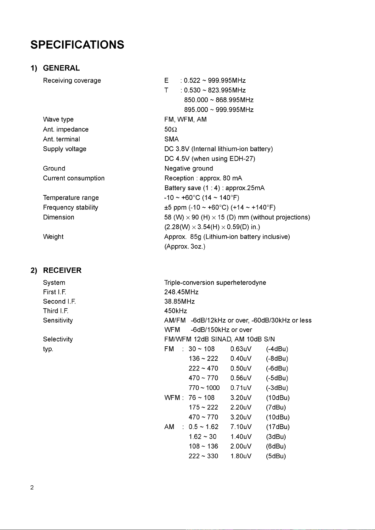
SPECIFICATIONS
1) GENERAL
Receiving coverage
Wave type
Ant. impedance
Ant. terminal
Supply voltage
Ground
Current consumption
Temperature range
Frequency stability
Dimension
Weight
E : 0.522 ~ 999.995MHz
T : 0.530 ~ 823.995MHz
850.000 ~ 868.995MHz
895.000 ~ 999.995MHz
FM, WFM, AM
50Q
SMA
DC 3.8V (Internal lithium-ion battery)
DC 4.5V (when using EDH-27)
Negative ground
Reception : approx. 80 mA
Battery save (1 : 4) : approx.25mA
-10 ~ +60°C (14 ~ 140°F)
±5 ppm (-10 ~ +60°C) (+14 ~ +140°F)
58 (W) x 90 (H) x 15 (D) mm (without projections)
(2.28(W) x 3.54(H) x 0.59(D) in.)
Approx. 85g (Lithium-ion battery inclusive)
(Approx. 3oz.)
2) RECEIVER
System
First I.F.
Second I.F.
Third I.F.
Sensitivity
Selectivity
typ.
Triple-conversion superheterodyne
248.45MHz
38.85MHz
450kHz
AM/FM -6dB/12kHz or over, -60dB/30kHz or less
WFM -6dB/150kHz or over
FM/WFM 12dB SINAD, AM 10dB S/N
FM : 30 ~ 108 0.63uV (-4dBu)
136~222 0.40uV (-8dBu)
222 ~ 470 0.50uV (-6dBu)
470 ~ 770 0.56uV (-5dBu)
770~1000 0.71uV (-3dBu)
WFM : 76 ~ 108 3.20uV (10dBu)
175~222 2.20uV (7dBu)
470 ~ 770 3.20uV (10dBu)
AM : 0.5 ~ 1.62 7.10uV (17dBu)
1.62 ~ 30 1.40uV (3dBu)
108~136 2.00uV (6dBu)
222 ~ 330 1.80uV (5dBu)
2
Page 4
CIRCUIT DESCRIPTION
1) Receiver
1. Receiver system : Triple Superheterodyne Conversion
1st IF. : 248.45MHz
2nd IF. : 38.85MHz
3rd IF. : 450KHz
2. Front End
0.5 ~ 29.995MHz
The signal from the antenna is switched by the band switch (D109), passed
through the low-pass filter and amplified by RF amplifier Q109. Then the
signal is fed to the 1st mixer IC103 via the band switch D115.
30 ~ 136.995MHz
The signal from the antenna is switched by the band switch (D128), passed
through the low-pass filter and amplified by RF amplifier Q111. Then the
signal is fed to the 1st mixer IC103 via the band switch D112.
137 ~ 222.995MHz
The signal from the antenna is switched by the band switch (D116), passed
through the low-pass filter and amplified by RF amplifier Q116. Then the
signal is fed to the 1st mixer IC103 via the band switches D107 and D129.
223 ~ 367.995MHz
368 ~ 469.995MHz
470 ~ 999.995MHz
3. Mixer
The 1st Mixer
The signal from the antenna is switched by the band switch (D132), passed
through the low-pass filter and amplified by RF amplifier Q118. Then the
signal is fed to the 1st mixer IC103 via the band switches D107 and D129.
The signal from the antenna is switched by the band switch (D122), passed
through the low-pass filter and amplified by RF amplifiers Q123 and Q138.
Then the signal is fed to the 1st mixer IC103 via the band switch D134.
The signal from the antenna is switched by the band switch (D133), passed
through the low-pass filter and amplified by RF amplifier Q126. Then the
signal is fed to the 1st mixer IC103 via the band switch D120.
The input signal and 1st local signal generate sum and difference frequencies
in the mixer IC103. SAW filter FL101 selects the signal of 248.45MHz and
eliminates the adjacent channel signals.
The 2nd Mixer
The input signal and the 2nd local signal generate sum and difference fre
quencies in the mixer IC104. Then the signals are divided into the receiving
sides of FM/AM and WFM at D113 and D114.
3
Page 5
FM/AM
WFM
4. IF
FM/AM
FM
In the receiving side of FM/AM the signal of 38.85MHz is selected by crystal
filter XF101. Then the signal is amplified at the 1st IF amplifier Q112 after
eliminating the adjacent channel signal.
In the receiving side of WFM the signal of 38.85MHz is selected by band-pass
filter. Then the signal is amplified at the 1st IF amplifier Q112 after eliminating
the adjacent channel signal.
The amplified signal at the 1st IF amplifier Q112 is led to the demodulator pin
24 of IC105. The signal of 12.8MHz from the reference buffer output of IC101
is multiplied by 3 in Q133. Then the signal is mixed with the signal of pin 1 of
IC105 in the mixer circuit inside of IC105 and converted into the 2nd IF signal
of 450kHz. The converted 2nd IF signal is output from pin 3 of IC105.
The output signal from pin 3 of IC105 is led to pin 7 of IC105 after eliminating
the adjacent channel signal at the ceramic filter FL103. The input 2nd IF
signal to pin 7 of IC105 is demodulated at the limiter amplifier and quadrature
detector circuits inside of IC105, then output from pin 12 of IC105 as an AF
signal.
AM
WFM
5. Squelch
The output signal from pin 3 of IC105 is led to the pin 5 of IC105 after eliminat
ing the adjacent channel signal at the ceramic filter FL103. The 2nd IF signal
input to pin 5 of IC105 is AM-demodulated inside of IC and output from pin 13
of IC105 as an AF signal. The 1st IF amplifier Q112 is controlled by reverse
AGC at AGC amplifier Q117 to get better audio output even though the input
is changed, and the gain is controlled.
The output signal from pin 3 of IC105 is led to pin 7 of IC105. The input 2nd IF
signal to pin 7 of IC105 is demodulated at the limiter amplifier and quadrature
detector circuits inside of IC, then output from pin 12 of IC105 as an AF signal.
The AF signal got from pin 12 of IC105 is fed to pin 19 of IC105. The input
signal is output from pin 21 of IC105 passing through the noise filter amplifier
and rectifier circuits inside of IC. The rectified signal is added to the A/D port
of the microcomputer IC1. Judging the signal, the microcomputer controls
ON/OFF of the audio output.
4
Page 6
6. Audio
FM/AM/WFM
7. VCO
The 1st Local
The 2nd Local
The selection of receiving audio output signal between FM/WFM and AM is
performed at IC106. The volume of output audio signal is adjusted at the
electronic volume IC108 via the AF amplifier Q120. After converting the im
pedance of the signal whose volume is adjusted at Q124, the signal is input to
pin 2 of audio power amplifier IC110 and output from pin 6 to drive a speaker,
etc.
The VCO for the 1st local consists of the Colpitts oscillator. D106, D108 and
L105 determine the frequency, and they are oscillated at the transistor Q103.
The oscillated signal is added to pin 2 of PLL-IC101 through the butter ampli
fiers Q105 and Q134.
The VCO for the 2nd local consists of the Colpitts oscillator. D110, D111 and
L113 determine the frequency, and they are oscillated at the transistor Q110.
The oscillated signal is added to pin 19 of PLL-IC101 through the butter am
plifier Q135.
8. PLL
The 1st Local
The 2nd Local
PLL-IC101 is used to control the oscillation frequency of VCO. The micro
computer IC1 sends the signal with serial data to control IC101. The 12.8
MHz reference frequency of IC101 oscillates the crystal oscillator X101 at the
inside circuit.
Using the control signal from IC1, IC101 compares the divided value of the
added signal to pin 2 of IC101 with the divided value of 12.8 MHz reference
frequency inside IC101. When the phase difference is occurred, IC101 out
puts the pulse signal from pin 8 and converts into DC voltage at the active filter
Q107 and Q108. Then it is fed to the cathode of the VCO vari-cap diodes of
D106 and D108 to reduce the phase difference. This brings the stable oscilla
tion at the desired frequency.
Using the control signal from IC1, IC101 compares the divided value of the
added signal to pin 19 of IC101 with the divided value of 12.8 MHz reference
frequency inside IC101. When the phase difference is occurred, IC101 out
puts the pulse signal from the charge pump output pin 13 and converts into
DC voltage at the inside circuit for the active filter. Then it is fed to the cathode
of the VCO vari-cap diodes of D110 and D111 to reduce the phase difference.
This brings the stable oscillation at the desired frequency.
5
Page 7
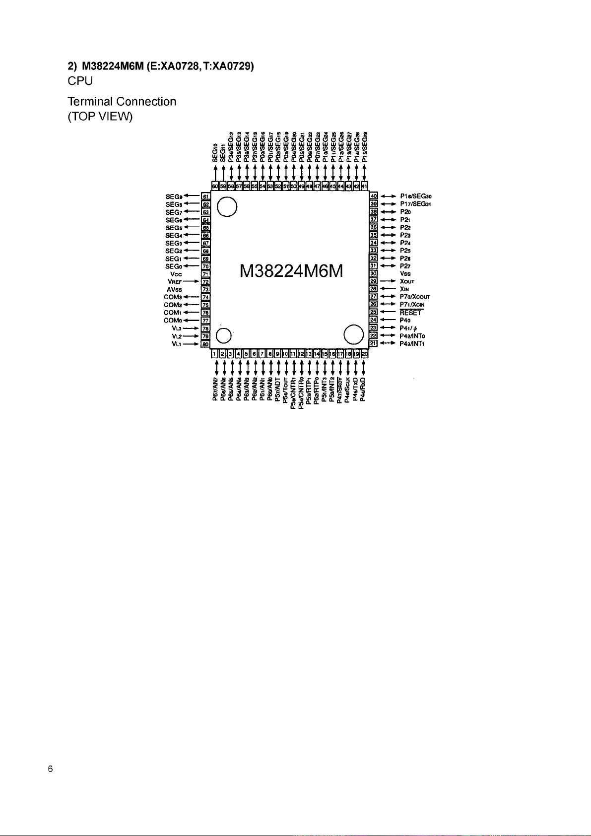
2) M38224M6M (E:XA0728, T:XA0729)
CPU
Terminal Connection
(TOP VIEW)
ssjssts-siiaaaa'aa&aa
000(900(300000000000
o »-LUUJUJlDLLILLJLUUJLULULiJLUliJlULLIlULlJlU
t m t m m m m m
SEGs-
SEGs”
SEG?-
SEGs"
SEGs-
SEG4-
SEG3-
SEG2-
SEGt-
SEGo-
Vco
Vh ef-
AVss
COM3-
COM2-
COM1-
COMo-
VL3-
VL2-
Vli -
i@ S T
o
M38224M6M
o O
4c0 ■*—►
3g| •*— ►
m ■*—* '
W + - +
36] -4—►
m ■*—►
m J ■*— ►
32] -«—►
ID -* —►
30)
1 1 — *-
10 •*—
w + - * >
m + —
¡ g * —
n * —
m ■*—►
13 *•—►
pi 6/segso
pi 7/SEG31
P2o
P21
P22
P23
P24
P25
P26
P27
Vss
XOUT
XlN
P7o/Xcout
P7i /Xcin
RESET
P4o
P4i/^
P42/1NTo
P4s/INTi
t t tw w w t w w t
!*&"»?> ^ ^
> CD <P (0 (O <0
. CL Ql CL CL O.
I— I - »- O w~ O « • »
5 5 (r QC Q. Q. I-
It s s l
K 1 a . 2 2 ^ 2 i a.
0 . Q.
I *
q a
6
Page 8
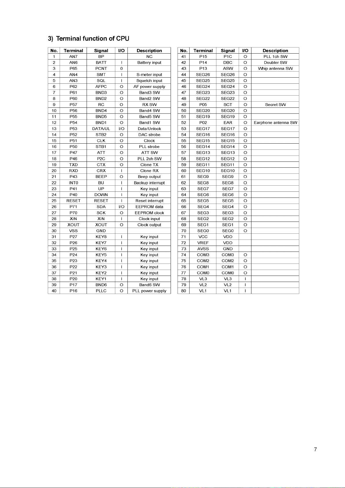
3) Terminal function of CPU
No. Terminal Signal I/O Description
1 AN7 BP NC
2 AN6 BATT I Battery input
3 P65 PCNT 0
4 AN4 SMT I S-meter input
5 AN3 SQL I Squelch input
6
P62 AFPC O AF power supply
7 P61 BND3 O Band3 SW
8 P60 BND2 O Band2 SW
9 P57 RC O RX SW
10 P56 BND4 O Band4 SW
11 P55 BND5 O Band5 SW
12 P54 BND1 O Band1 SW
13 P53 DATA/UL I/O Data/Unlock
14 P52 STB2 O DAC strobe
15 P51 CLK O Clock
16 P50 STB1 O PLL strobe
17 P47 ATT O ATT SW
18 P46 P2C O PLL 2ch SW
19 TXD CTX O Clone TX
20 RXD CRX I Clone RX
21 P43 BEEP O Beep output
22 INT0 BU I Backup interrupt
23 P41 UP I Key input
24 P40 DOWN I Key input
25 RESET RESET I Reset interrupt
26 P71 SDA I/O EEPROM data
27 P70 SCK O EEPROM clock
28 XIN XIN I Clock input
29 XOUT XOUT O Clock output
30 VSS GND
31 P27 KEY8 I Key input
32 P26 KEY7 I Key input
33 P25 KEY6 I Key input
34 P24 KEY5 I Key input
35 P23 KEY4 I Key input
36 P22 KEY3 I Key input
37 P21 KEY2 I Key input
38 P20 KEY1 I Key input
39 P17 BND6 O Band6 SW
40 P16 PLLC O PLL power supply
No. Terminal Signal I/O Description
41 P15 P1C O PLL 1ch SW
42 P14 DBC O Doubler SW
43 P13 ASW O Whip antenna SW
44 SEG26 SEG26 O
45 SEG25 SEG25 O
46 SEG24 SEG24 O
47 SEG23 SEG23 O
48 SEG22 SEG22 O
49 P05 SCT O Secret SW
50 SEG20 SEG20 O
51 SEG19 SEG19 O
52 P02 EAR O Earphone antenna SW
53 SEG17 SEG17 O
54 SEG16 SEG16 O
55 SEG15 SEG15 O
56 SEG14 SEG14 O
57 SEG13 SEG13 O
58 SEG12 SEG12 O
59 SEG11 SEG11 O
60 SEG10 SEG10 O
61 SEG9 SEG9 O
62 SEG8 SEG8 O
63 SEG7 SEG7 O
64 SEG6 SEG6 O
65 SEG5 SEG5 O
66 SEG4 SEG4 O
67 SEG3 SEG3 O
68 SEG2 SEG2 O
69 SEG1 SEG1 O
70 SEG0 SEG0 O
71 VCC VDD
72 VREF VDD
73 AVSS GND
74 COM3 COM3 O
75 COM2 COM2 O
76 COM1 COM1 O
77 COMO COM0 O
78 VL3 VL3 I
79 VL2 VL2 I
80 VL1 VL1 I
7
Page 9
SEMICONDUCTOR DATA
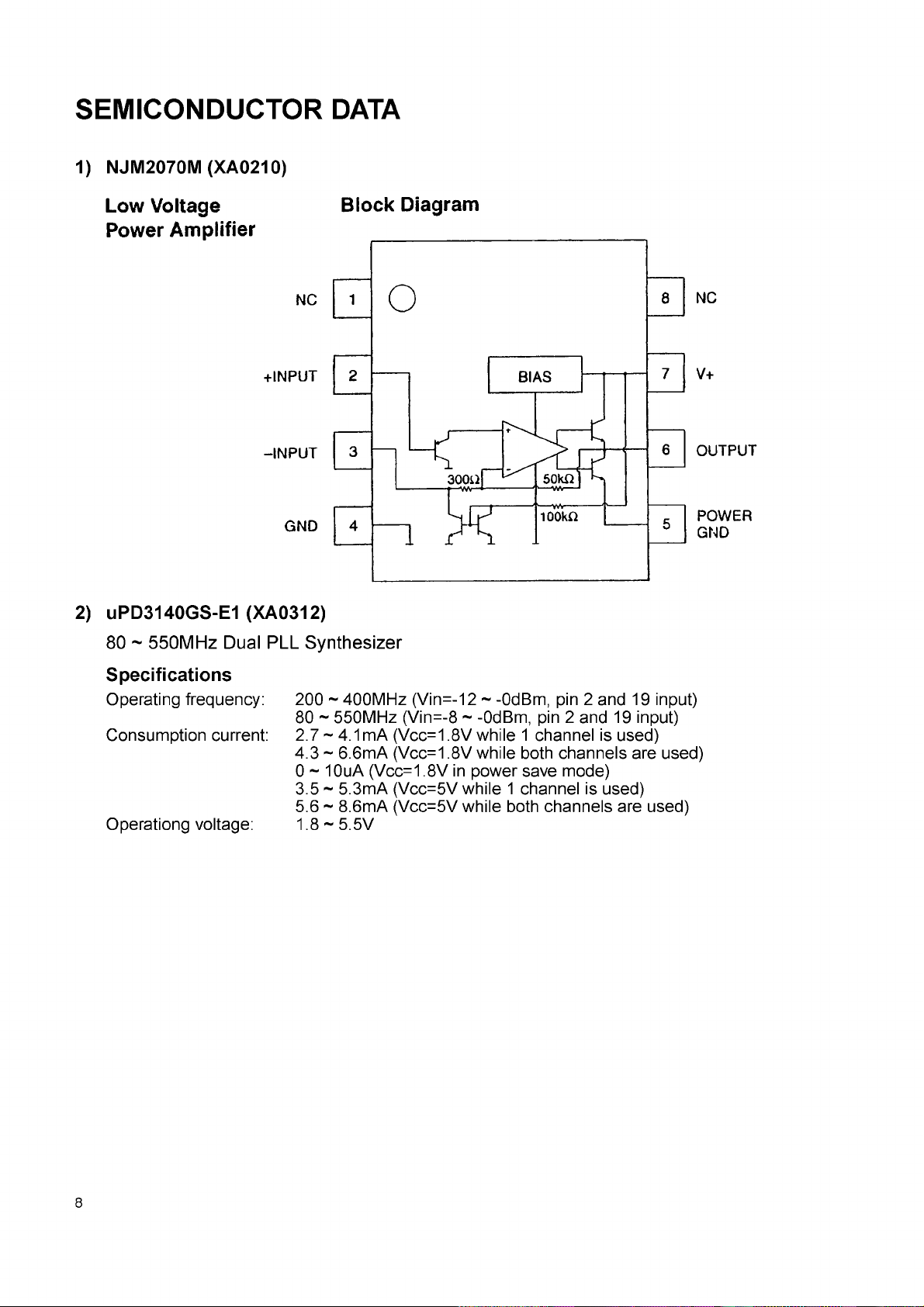
1) NJM2070M (XA0210)
2) uPD3140GS-E1 (XA0312)
80 ~ 550MHz Dual PLL Synthesizer
Specifications
Operating frequency:
Consumption current:
Operationg voltage:
200 ~ 400MHz (Vin=-12 ~ -0dBm, pin 2 and 19 input)
80 ~ 550MHz (Vin=-8 ~ -0dBm, pin 2 and 19 input)
2.7 ~ 4.1mA (Vcc=1.8V while 1 channel is used)
4.3 ~ 6.6mA (Vcc=1.8V while both channels are used)
0 ~ 10uA (Vcc=1.8V in power save mode)
3.5 ~ 5.3mA (Vcc=5V while 1 channel is used)
5.6 ~ 8.6mA (Vcc=5V while both channels are used)
1.8 ~ 5.5V
8
Page 10
Block Diagram
3) TC4W53FU (XA0348)
Pin Assignment
COMMON
1NH
VEE
VSS
[T
H
[I
\L
0
3
3
I]
H
VDD
ch 0
ch 1
A
Block Diagram
(8 ) VDD
1..JL
......
© 4 M
A :
INH - - - I -
sir
VSS VEE
OUT IN
OUT IN
COMMON
!ch 1
9
1-
Page 11
4) S-80730SL-AT (XA0356)
5) M5222FP-600C (XA0385)
Electronic Volume
10
Page 12
6) XC62SPR332MR (XA0519)
Pin Assignment Block Diagram
7) NJM2904V (XA0573)
Dual Single Supply Operational Amplifer
11
Page 13

8) MB88347LPFV-G-BND-EF (XA0599)
D/A converter for digital tuning
12
Page 14

OSC(B)
OSC(E)
Pin Assignment / BLOCK Diagram (Top View)
MIX OUTPUT
AM IF INPUT
DECOUPLING
FM IF INPUT
DECOUPLING
DECOUPLING
LIM OUTPUT
QUAD INPUT
COMP OUTPUT
COMP INPUT
NOISE AMP OUTPUT
05
J' £ c \ r f
>
\ /
> v \ /
1
Vref
>
CD
O
■ O ,
NOISE AMP INPUT
5
AM AGO INPUT
AGO AMP OUTPUT
“0
-\W— "
ZJ
C/)
C/)
RFAGC OUTPUT
RSSI OUTPUT
FM DET OUTPUT >o *
co AM DETOUT
r
Page 15

10) TK10931V (XA0666)
CD T)
O
O
7T
O
0)'
(Q
3
3
O
C/3
O
O
7s
O
7s
9) TK11816M (XA0665)
u '
>
(/)
(/)
cq '
=3
3
(D
O
7s
Page 16

11) TA4101F TE12L (XA0667)
Pin Assignment
8 7 6 5
n n n n
u u u u
1 2 3 4
1. IF OUT 5. BASE
2. Vcc 6. BASE
3. O SC IN 7. GND
4. BASE 8. COLLECTO R
12) S-80829ALNP-EAS-T2 (XA0668)
Pin Assignment
4
Top view
Block Diagram
R2 S RB3
HVW
3
1 O UT
8
1
4
6
7
3
Block Diagram
2 V dd
3 NC
4 Vss
14
Page 17

13) BR24C64F-E2 (XA0669)
Block Diagram
AO i
Ai 2
A2 3
GND 4
4
Pin Assignment
i3bit
ADDRESS
DECODER
CO NTRO L C IR CUIT
I
HIGH VOLTAGE
GENERATOR
Vcc WP SCL SDA
64Kbit EE PROM A RRAY
i3b it
START STOP
SLAVE^WORD
ADDRESS REGISTER
VOLTAGE
DETECTOR
ACK
DATA
REGISTER
H
r
8 Vcc
7 WP
6 SCL
BR24C64/F
o
AO Ai A2 GND
iS
Page 18

14) uPC2757T-E3 (XA0743)
Terminal Connection
(Top View) (Bottom View)
3 H
2 H
1 m
Block Diagram
X
r >
□ 4 4 C
□ 5 5 1!
U
1: RF input 4: PS (Power Save)
2: GN D 5: Vcc
3: Lo input 6: IF output
□ 6 6 H
O
3
2
1
input
16
Page 19

15) Transistor, Diode and LED Outline Drawings
1SV308(TPH3)
""xD0339 " '
SML-310MTT86
""x'D0036'""
- 4
2SK881Y(TE85R)
......
x Eo036
........
s
K Y
DAN235E-TL
""""xDÖ32Ö"""
MA2S357-Tx
""" XD0337"""'
ISS390 TE61
xDd342
MA2S30400L
"xD03"í2
......
MA2S728-Tx
x"DO"3Í5"
A
B
-----
B
M
2SC4738BL(TE85R)
......
xT0í8"í
n n n n n n
L L M 2 Y R V Y M A
UMC5NTR
"'xu'di'S'i'"
2SC5066FT-Y(TE85L)
.......
......
""x'U0'd92""
N
xTöisO.........
UN911H Tx
C
6 R
2SD2216R-Tx
" " x t OVSS
DTC143TE TL
""xUÖV96
C
O 3
......
......
f t f t
2SJ144Y(TE85R))
......
xEboig
......
x p i i i i-tx
"'x 'U 0i7i'"
2SC5O96FT-O(TE85L)
........
xT0i 82
.......
ISS362 TE85L
xD0338
*
C3
2SC4618TL
'''x T0i72'"
A Í J
17
Page 20

16) LCD connection
LCD Common
LCD Segment
18
Page 21

EXPLODED VIEW
1) Front View
AX0005
AP0027
19
Page 22

2) Rear View
PR0309 (*E)
20
Page 23

PARTS LIST
Ref.
Parts No. Description Parts Name X2
No.
CPU Unit
YX 0004 TAPE
C1 CU3535 Chip C. GRM 36B102K50PT
C2 CU3111 Chip C. C1608JB1C104KT-N
C3 CU3111 Chip C. C1608JB1C104KT-N
C300 CS0403 Chip Tantal TMCP1D224MTR
C4 CU3547 Chip C. GRM 36B103K16PT
C5 CU3517 Chip C. GRM3 6CH330J50PT
C6 CU3517 Chip C. GRM3 6CH330J50PT
C7 CS0398 Chip Tantal TMCP0J225MTR
C8 CU3111 Chip C. C1608JB1C104KT-N
C9 CS0398 Chip Tantal TMCP0J225MTR
CN1 UE0403 Connector AXK 5S3024
D1 XD0315 Diode MA2S728-TX
IC1 XA0729 IC M38224M6M-142HP E
IC1 XA0728 IC M38224M6M-141HP T
IC2 XA0356 IC S-80730SL-AT-T1
IC3 XA0669 IC BR 24C64F-E2
L1 Q C0507 Coil LK160 81R0K-T
XU0152 Transistor UMC5NTR
Q1
R1 RK3542 Cihp R. ERJ2GEJ222X
R13 RK3550 Cihp R. ERJ2GEJ103X
R14 RK3538 Cihp R. ERJ2GEJ102X
R15 RK3559 Cihp R. ERJ2GEJ563X
R16 RK3526 Cihp R. ERJ2GEJ101X
R17 RK3562 Cihp R. ERJ2G EJ104X
R18 RK3538 Cihp R. ERJ2GEJ102X
R19 RA0009 Cihp R. EXBV8V102JV
R20 RK3562 Cihp R. ERJ2GEJ104X
R21 RK3562 Cihp R. ERJ2GEJ104X
R22 RA0009 Cihp R. EXBV8V102JV
R23 RK3562 Cihp R. ERJ2G EJ104X
R24 RK3562 Cihp R. ERJ2G EJ104X
R25 RK3562 Cihp R. ERJ2G EJ104X
R26 RA0008 Cihp R. EXBV4V102JV
R3 RK3558 Cihp R. ERJ2GEJ473X
R4 RK3558 Cihp R. ERJ2GEJ473X
R6 RK3558 Cihp R. ERJ2GEJ473X
R7 RK3558 Cihp R. ERJ2GEJ473X
R8 RK3558 Cihp R. ERJ2GEJ473X
X1 XQ 0132 Crystal C SA309/4.1943MHz
MAIN Unit
UT0042 JY U DENTANSIXH 662
TS0160 VCO CASE
C101 CU3111 Chip C. C1608JB1C104KT-N
C102 CU3111 Chip C. C1608JB1C104KT-N
C103 CU3111 Chip C. C1608JB1C104KT-N
C104 CU3515 Chip C. GRM 36CH 220J50PT
C105 CU3535 Chip C. GRM36B102K50PT
C106 CU3111 Chip C. C1608JB1C104KT-N
C107 CU3506 Chip C. GRM 36CH050C50P T
C108 CU3535 Chip C. GRM36B102K50PT
C109 CS0411 Chip Tantal 4M CM226MATER
C110 CU3535 Chip C. GRM36B102K50PT
C111 CU3512 Chip C. GRM36CH120J50PT
C112 C U3503 Chip C. GRM36CK020C50PT
C113 CU3111 Chip C. C1608JB1C104KT-N
C114 CU3547 Chip C. GRM36B103K16PT
C115 CU3511 Chip C. GRM 36CH100D50PT
C116 CU3523 Chip C. GRM36CH101J50PT
C117 CU3511 Chip C. GRM 36CH100D50PT
Ref.
Parts No. Description Parts Name X2
No.
C118 CU3547 Chip C. GR M36B103K16PT
C119 CS 0396 Chip Tantal TMCP1D104MTR
C120 CU3501 Chip C. GRM36C K0R5C50PT
C121 CU3547 Chip C. GRM36B103K16PT
C122 CS0408 Chip Tantal 6M CM156MATER
C123 CU3523 Chip C. GRM 36CH 101J50PT
C124 CU3535 Chip C. GR M36B102K50PT
C125 CS0397 Chip Tantal TMCP1C105MTR
C126 CU3535 Chip C. GRM36B102K50PT
C127 CS0396 Chip Tantal TMCP1D104MTR
C128 CS0397 Chip Tantal TMCP1C105MTR
C129 CU3535 Chip C. GRM36B102K50PT
C130 CU3111 ChipC. C1608JB1C104KT-N
C131 CU3111 ChipC. C1608JB1C104KT-N
C132 CU3547 Chip C. GR M36B103K16PT
C133 CU3547 Chip C. GR M36B103K16PT
C134 CU3111 ChipC. C1608JB1C104KT-N
C135 CS0397 ChipTantal TMCP1C105MTR
C136 CU3111 ChipC. C1608JB1C104KT-N
C137 CU3111 ChipC. C1608JB1C104KT-N
C138 CU3531 Chip C. GRM 36B471K50PT
C139 CU3547 Chip C. GRM36B103K16PT
C140 CU3503 Chip C. GR M36C K020C50PT
C141 C U3503 Chip C. GR M36C K020C50PT
C142 C U3503 Chip C. GR M36C K020C50PT
C143 CU3535 Chip C. GRM36B102K50PT
C144 CU3535 Chip C. GRM36B102K50PT
C145 CU3111 Chip C. C1608JB1C104KT-N
C146 CU3505 Chip C. GRM36CH040C50PT
C147 CU3523 Chip C. GR M 36CH 101J50PT
C148 CU3527 Chip C. GRM 36CH 221J25PT
C149 CU3527 Chip C. GR M 36CH 221J25PT
C150 CU3523 Chip C. GR M 36CH 101J50PT
C151 C U3535 Chip C. GRM36B102K50PT
C152 CU3501 Chip C. GR M36C K0R5C50PT
C153 CU3111 Chip C. C1608JB1C104KT-N
C154 CU3111 Chip C. C1608JB1C104KT-N
C155 CU3535 Chip C. GRM36B102K50PT
C156 CU3509 Chip C. GRM3 6CH080D50PT
C157 CS0411 Chip Tantal 4M CM226MATER
C158 CU3527 ChipC. GRM 36CH 221J25PT
C159 CS0397 Chip Tantal TMCP1C105MTR
3
C160 CU3527 Chip C. GRM36CH221J25PT
C161 CU3502 Chip C. GR M36C K010C50PT
2
C162 CU3535 Chip C. GRM36B102K50PT
C163 CU3503 Chip C. GR M36C K020C50PT
C164 CU3514 Chip C. GRM 36CH 180J50PT
C165 CU3011 Chip C. C1608CH1H100DT-AS
C166 CU3535 Chip C. GR M36B102K50PT
C167 CU3547 Chip C. GRM36B103K16PT
C168 CU3111 Chip C. C1608JB1C104KT-N
C169 CU3547 Chip C. GR M36B103K16PT
C170 CU3547 Chip C. GRM36B103K16PT
C171 CU3547 Chip C. GR M36B103K16PT
C172 CU3547 Chip C. GRM36B103K16PT
C173 CU3547 Chip C. GRM36B103K16PT
C174 CU3021 Chip C. C1608CH1H680JT-AS
C175 CU3021 Chip C. C1608CH1H680JT-AS
C176 CU3516 Chip C. GRM 36CH 270J50PT
C177 CU3547 Chip C. GRM36B103K16PT
C178 CU3509 Chip C. GRM3 6CH080D 50PT
21
Page 24

Ref.
Parts No. Description Parts Name X2
No.
C179 CU3502 Chip C. GRM36CK010C50PT
C180 CU3517 Chip C. GRM3 6CH330J50PT
C181 CU3020 Chip C. C1608CH1H560JT-AS
C182 CU3517 Chip C. GRM3 6CH330J50PT
C183 CU3547 Chip C. GRM36B103K16PT
C184 CU3551 Chip C. GRM 36B223K16PT
C185 CU3535 Chip C. GRM36B102K50PT
C186 CU3535 Chip C. GRM36T
C187 CU3535 Chip C. GRM36B102K50PT
C188 CU3523 Chip C. GRM 36CH 101J50PT
C189 CU3523 Chip C. GRM3 6CH101J50PT
C190 CU3111 Chip C. C1608JB1C104KT-N
C191 CU3547 Chip C. GRM36B103K16PT
C192 CU3535 Chip C. GRM36B102K50PT
C193 CS0404 Chip Tantal 6M CM106MATER
C194 CU3013 Chip C. C1608CH1H150JT-AS
C196 CU3535 Chip C. GRM36B102K50PT
C197 CU3551 Chip C. GRM 36B223K16PT
C198 CU3551 Chip C. GRM 36B223K16PT
C199 CU3535 Chip C. GRM36B102K50PT
C200 CU3535 Chip C. GRM36B102K50PT
C201 CU3535 Chip C. GRM36B102K50PT
C202 CU3509 Chip C. GRM36CH080D50PT
C203 CU3509 Chip C. GRM 36CH080D50P T
C204 CU3518 Chip C. GRM3 6CH390J50PT
C205 CU3512 Chip C. GRM36CH120 J50PT
C206 CU3033 Chip C. C1608JB1H681KT-AS
C207 CU3516 Chip C. GRM3 6CH270J50PT
C208 CU3020 Chip C. C1608CH1H560JT-AS
C209 CU3516 Chip C. GRM3 6CH270J50PT
C210 CU3547 Chip C. GRM36B103K16PT
C211 CU3535 Chip C. GRM36B102K50PT
C212 CU3111 Chip C. C1608JB1C104KT-N
C213 CU3111 Chip C. C1608JB1C104KT-N
C214 CU3111 Chip C. C1608JB1C104KT-N
C215 CU3511 Chip C. GRM36CH100D 50PT
C216 CU3535 Chip C. GRM36B102K50PT
C217 CU3547 Chip C. GRM36B103K16PT
C218 CU3535 Chip C. GRM36B102K50PT
C219 CS0411 Chip Tantal 4MCM 226MATER
C220 CU3535 Chip C. GRM36B102K50PT
C221 CU3111 Chip C. C1608JB1C104KT-N
C222 CU3019 Chip C. C1608CH1H470JT-AS
C223 CU3535 Chip C. GRM36B102K50PT
C224 CU3506 Chip C. GRM36CH050C50PT
C225 CU3506 Chip C. GRM36CH050C50PT
C226 CU3535 Chip C. GRM36B102K50PT
C227 CS0408 Chip Tantal 6M CM156MATER
C228 CU3547 Chip C. GRM36B103K16PT
C229 CU3547 Chip C. GRM36B103K16PT
C230 CU3547 Chip C. GRM36B103K16PT
C231 CU3547 Chip C. GRM36B103K16PT
C232 CU3111 Chip C. C1608JB1C104KT-N
C233 CS0408 Chip Tantal 6M CM156MATER
C234 CU3514 Chip C. GRM3 6CH180J50PT
C235 CU3517 Chip C. GRM3 6CH330J50PT
C236 CU3514 Chip C. GRM3 6CH180J50PT
C237 CU3111 Chip C. C1608JB1C104KT-N
C238 CU3531 Chip C. GRM 36B471K50PT
C239 CS0408 Chip Tantal 6M CM156MATER
C240 CU3531 Chip C. GRM 36B471K50PT
Ref.
Parts No. Description Parts Name X2
No.
C241 CU3111 Chip C. C1608JB1C104KT-N
C242 CS0396 Chip Tantal TMCP1D104MTR
C243 CU3531 Chip C. GRM 36B 471K50PT
C244 CS0398 Chip Tantal TM CP0J225MTR
C245 CU3511 Chip C. GRM36CH100D50PT
C246 CU3535 Chip C. GRM36B102K50PT
C247 CU3503 Chip C. GRM36CK020C50PT
C248 CU 3503 Chip C. GRM 36CK020C50P T
C249 CU3535 Chip C. GRM36B102K50PT
C250 CU3008 Chip C. C1608CH1H070CT-A
C251 CS0397 Chip Tantal TMCP1C105MTR
C252 CU3111 Chip C. C1608JB1C104KT-N
C253 CU3514 Chip C. GR M 36CH 180J50PT
C254 CU3517 Chip C. GR M 36CH 330J50PT
C255 CU3515 Chip C. GRM36CH220J50PT
C256 CU3551 Chip C. GRM36B223K16PT
C257 CS0414 Chip Tantal 6M CM476MB TER
C258 CU3111 Chip C. C1608JB1C104KT-N
C259 CU3111 Chip C. C1608JB1C104KT-N
C260 CU3535 Chip C. GRM36B102K50PT
C261 C U3547 Chip C. GRM36B103K16PT
C262 CU3111 Chip C. C1608JB1C104KT-N
C264 CS0411 Chip Tantal 4M CM226MATER
C265 CU3111 Chip C. C1608JB1C104KT-N
C266 CU3518 Chip C. GRM36CH390J50PT
C267 CU3547 Chip C. GRM36B103K16PT
C268 CU3535 Chip C. GRM36B102K50PT
C269 CS0412 Chip Tantal. 16MCM156MBTER
C270 CU3535 Chip C. GR M36B102K50PT
C271 CS0414 Chip Tantal 6M CM476MBTER
C272 CU3531 Chip C. GR M36B471K50PT
C273 CU3531 Chip C. GR M36B471K50PT
C274 CU3535 Chip C. GRM36B102K50PT
C275 CU3531 Chip C. GRM36B471K50PT
C276 CS0414 Chip Tantal 6M CM476MBTER
C277 CS0413 Chip Tantal 6M CM107MCTER
C278 CU3535 Chip C. GRM36B102K50PT
C279 CU3531 Chip C. GR M36B471K50PT
C280 CU3511 Chip C. GRM36CH100D50PT
C281 C U3505 Chip C. GRM36CH040C50PT
C282 C U3505 Chip C. GRM36CH040C50PT
C283 CU3007 Chip C. C1608CH1H060CT-A
C284 CU3547 Chip C. GRM 36B 103K16PT
C285 CU3535 Chip C. GRM36B102K50PT
C286 CU3547 Chip C. GR M36B103K16PT
C287 CU3547 Chip C. GR M36B103K16PT
C288 CU3111 Chip C. C1608JB1C104KT-N
C289 CS0413 Chip Tantal 6MC M 107MCTER
C290 CU3535 Chip C. GRM36B102K50PT
C291 CU3111 Chip C. C1608JB1C104KT-N
C292 C U3547 Chip C. GRM36B103K16PT
C293 CU3547 Chip C. GRM36B103K16PT
C294 CU3512 Chip C. GR M 36C H120J50PT
C295 CU3515 Chip C. GRM36CH220J50PT
C296 CU3021 Chip C. C1608CH1H680JT-AS
C297 CU3111 Chip C. C1608JB1C104KT-N
C298 CU3535 Chip C. GRM36B102K50PT
C299 CU3531 Chip C. GRM36B471K50PT
C301 C U3515 Chip C. GR M 36CH 220J50PT
C302 C U3535 Chip C. GRM36B102K50PT
C303 CU3518 Chip C. GR M 36CH 390J50PT
22
Page 25

Ref.
Parts No. Description Parts Name X2
No.
C3Ö4 CU3535 Chip C. GRM36B1Ö2K5ÖPT
C3Ö5 CU35Ö5 Chip C. GRM36CHÖ4ÖC5ÖPT
C3Ö6 CU35Ö6 Chip C. GRM36CHÖ5bC5bPT
C3Ö7 C U 3 ii i Chip C. C i6ÖBJBiCib4KT-N
C3ÖB CU3535 Chip C. G RM36BiÖ2K5ÖPT
C3Ö9 CU3523 Chip C. GRM36CH1Ö1J5ÖPT
C3ib CU3535 Chip C. GRM36BiÖ2K5ÖPT
C N ib i UEÖ396 Connector AXK6S3Ö645P
CN1Ö2 UEÖ32Ö Connector PI2BBÖ2M
D ib i XDÖ339 Diode ÍSV 30B
Dib2 XDÖ339 Diode ÍSV30B
DiÖ3 XDÖ32Ö Diode DAN235E-TL
DiÖ4 XDÖ33B Diode 1SS362
DiÖ5 XDÖ32Ö Diode DAN235E-TL
DiÖ6 XDÖ337 Diode MA2S357
D1Ö7 XDÖ32Ö Diode DAN235E-TL
DibB XDÖ337 Diode MA2S357
DiÖ9 XDÖ339 Diode 1SV3Ö8
D ii b XDÖ312 Diode MA2S3Ö4bbL
D iii XDÖ3i2 Diode MA2S3Ö4bbL
D ii2 XDÖ342 Diode iSS39b
D ii3 XDÖ32Ö Diode DAN235E-TL
D ii4 XDÖ32Ö Diode DAN235E-TL
D ii5 XDÖ339 Diode ÍSV30B
D ii6 XDÖ339 Diode ÍSV30B
D117 XDÖ32Ö Diode DAN235E-TL
D iiB XDÖ32Ö Diode DAN235E-TL
D ii9 XLÖÖ36 LED SML-31ÖM TT86
Di2 b XDÖ339 Diode ÍSV30B
D i2 i XDÖ32Ö Diode DAN235E-TL
Di22 XDÖ339 Diode ÍSV30B
Di23 XDÖ32Ö Diode DAN235E-TL
Di24 XDÖ339 Diode ÍSV30B
Di25 XDÖ339 Diode ÍSV30B
Di26 XDÖ339 Diode ÍSV30B
D127 XDÖ339 Diode ÍSV30B
D128 XDÖ342 Diode iSS39b
D129 XDÖ339 Diode 1SV3Ö8
D13Ö XDÖ339 Diode ÍSV30B
Di32 XDÖ339 Diode ÍSV30B
Di33 XDÖ339 Diode ÍSV30B
Di34 XDÖ339 Diode ÍSV30B
Di35 XDÖ342 Diode iSS39b
Di36 XDÖ342 Diode iSS39b
Di37 XDÖ33B Diode 1SS362
FL1Ö1 XCÖÖ7i Filter WF477A
FLib3 XCÖÖ75 Filter CFUCG45ÖE
IC ib i XAÖ3i2 IC UPD3i4Ö GS-E i
IC1Ö2 XAÖ599 IC MB88347LPFV-G-BND-EF
IC ib3 XAÖ743 IC uPC2757T
IC1Ö4 XAÖ743 IC uPC2757T
IC1Ö5 XAÖ666 IC T K ib 9 3iV
IC1Ö6 XAÖ34B IC TC4W53FU (TEi2)
IC1Ö7 XAÖ667 IC T A 4ibiF
ICibB XAÖ3B5 IC M5222FP-6ÖÖC
IC1Ö9 XAÖ665 IC T K iiBi6M TL
IC iib XAÖ2ib IC NJM2Ö7ÖM T i
IC i i i XAÖ573 IC NJM29Ö4V-TE1
IC ii2 XAÖ519 IC XC62SPR 332M R
IC ii3 XAÖ66B IC S-8Ö829ALNP
JKibi UJÖÖ44Z Jack H SJ i6 2 i-b i 9 bii
Ref.
Parts No. Description Parts Name X2
No.
Libi QCÖ56Ö Co LL16Ö8-FH8N2J
Lib2 QCÖ564 Co LL16ÖB-FH1BNJ
Lib3 QHbbb7 Co 5CDM 65BAN
Lib5 QCÖ586 Co LQW16bBA15NJbb
Lib6 QCÖ51Ö Co LK16bB33ÖM-T
Lib7 QCÖ6bb Co LQW16ÖBAR22Jbb
LibB QCÖ6bb Co LQW16ÖBAR22Jbb
Li 09 QCÖ6bb Co LQW16ÖBAR22Jbb
L i ib QCÖ569 Co LL16ÖB-FH47NJ
L i i i QCÖ5Ö6 Co LK16ÖBR56K-T
L112 QCÖ57Ö Co LL16Ö8-FH56NJ
L ii 3 QCÖ59Ö Co LQW16ÖBA33NJbb
L ii 4 QCÖ633 Co MLF16ÖBAR1BK-T
L ii 5 QCÖ596 Co LQW16bBAR1ÖJbb
L ii 6 QCÖ596 Co LQW16bBAR1ÖJbb
L ii 7 QCÖ571 Co LL16ÖB-FH6BNJ
LiiB QCÖ6bb Co LQW16ÖBAR22Jbb
L ii 9 QCÖ597 Co LQW16bBAR12Jbb
L12Ö QCÖ6bb Co LQW16ÖBAR22Jbb
Li2i QCÖ56B Co LL16ÖB-FH39NJ
Li22 QCÖ596 Co LQW16Ö8AR1ÖJÖÖ
123 QCÖ596 Co LQW16bBAR1ÖJbb
Li2 4 QCÖ5Ö7 Co LK16bB1RÖK-T
Li2 5 QCÖ566 Co LL16ÖB-FH27NJ
Li2 6 QCÖ5B9 Co LQW16ÖBA27NJbb
Li2 7 QCÖ5B6 Co LQW16bBA15NJbb
Li2B QCÖ5B9 Co LQW16ÖBA27NJbb
Li2 9 QCÖ564 Co LL16ÖB-FH1BNJ
Li3b QCÖ593 Co LQW16ÖBA56NJbb
Li3i QCÖ593 Co LQW16ÖBA56NJbb
Li32 QCÖ5B6 Co LQW16Ö8A15NJÖÖ
Li3 3 QCÖ5B3 Co LQW16ÖBABN2Dbb
Li3 4 QCÖ5B6 Co LQW16bBA15NJbb
Li3 5 QCÖ562 Co LL16ÖB-FH12NJ
L136 QCÖ593 Co LQW16ÖBA56NJbb
L137 QCÖ593 Co LQW16ÖBA56NJbb
L138 QCÖ497 Co LQH4N1b2KÖ4
L139 QCÖ497 Co LQH4N1Ö2KÖ4
L14Ö QCÖ5B1 Co LQW16ÖBA5N6Dbb
Li4i QCÖ579 Co LQW16ÖBA3N9Dbb
Li42 QCÖ5B1 Co LQW16Ö8A5N6DÖÖ
Li4 3 QCÖ5B7 Co LQW16ÖBA1BNJbb
Li4 4 QCÖ5B5 Co LQW16ÖBA12NJbb
Li4 5 QCÖ585 Co LQW16ÖBA12NJbb
L146 QCÖ555 Co LL16ÖB-FH3N3S
L147 QCÖ573 Co LL16bB-FHR1ÖJ
L148 QCÖ562 Co LL16ÖB-FH12NJ
L149 QCÖ5Ö7 Co LK16bB1RÖK-T
L15Ö QCÖ5Ö7 Co LK16bB1RÖK-T
L151 QCÖ5Ö7 Co LK16bB1RÖK-T
L152 QCÖ5Ö7 Co LK16Ö81RÖK-T
L153 QCÖ5Ö6 Co LK16ÖBR56K-T
L154 QCÖ56Ö Co LL16ÖB-FHBN2J
L155 QCÖ564 Co LL16ÖB-FH1BNJ
L156 QCÖ555 Co LL16ÖB-FH3N3S
L157 QCÖ56Ö Co LL16ÖB-FHBN2J
LCD1 ELÖÖ4B LCD LCD XH757
Q1Ö1 XTÖ1BÖ Transistor 2SC5Ö66FT-Y
Q1Ö2 XUÖ196 Transistor DTC143TE
Q1Ö3 XTÖ1BÖ Transistor 2SC5Ö66FT-Y
Q1Ö4 XUÖÖ92 Transistor UN911H-TX
23
Page 26

Ref.
Parts No. Description Parts Name X2
No.
Q105 XT0180 Transistor 2SC5066FT-Y
Q106 XU0196 Transistor DTC143TE
Q107 XT0181 Transistor 2SC4738-BL
Q108 XT0181 Transistor 2SC4738-BL
Q109 XT0180 Transistor 2SC5066FT-Y
Q110 XT0180 Transistor 2SC5066FT-Y
Q111 XT0172 Transistor 2SC4618TLP
Q112 XT0181 Transistor 2SC4738-BL
Q113 XU0171 Transistor XP 1111-TX
Q114 XU0171 Transistor XP 1111-TX
Q115 XU0171 Transistor XP 1111-TX
Q116 XT0180 Transistor 2SC5066FT-Y
Q117 XT0135 Transistor 2SD2216R-TX
Q118 XT0180 Transistor 2SC5066FT-Y
Q119 XU0092 Transistor UN911H-TX
Q120 XT0135 Transistor 2SD2216R-TX
Q121 XU 0092 Transistor UN911H-TX
Q122 XU0196 Transistor DTC143TE
Q123 XT0182 Transistor 2SC50 96FT-0
Q124 XT0135 Transistor 2SD2216R-TX
Q125 XU0152 Transistor UMC5NTR
Q126 XT0182 Transistor 2SC50 96FT-0
Q127 XU0171 Transistor XP 1111-TX
Q128 XU0171 Transistor XP 1111-TX
Q129 XU0171 Transistor XP 1111-TX
Q130 XU0171 Transistor XP 1111-TX
Q131 XU0171 Transistor XP1111-TX
Q132 XT0135 Transistor 2SD2216R-TX
Q133 XT0180 Transistor 2SC5066FT-Y
Q134 XT0180 Transistor 2SC5066FT-Y
Q135 XT0180 Transistor 2SC5066FT-Y
Q136 XU0196 Transistor DTC143TE
Q137 XU0152 Transistor UMC5NTR
Q138 XT0180 Transistor 2SC5066FT-Y
Q139 XT0135 Transistor 2SD2216R-TX
Q140 XE0036 FET 2SK881-Y(TE85R)
Q141 XE0019 FET 2SJ144Y TE85R
RK3542 Cihp R. ERJ2GEJ222X
R101
R102 RK3522 Cihp R. ERJ2GEJ470X
R103 RK3542 Cihp R. ERJ2GEJ222X
R104 RK3542 Cihp R. ERJ2GEJ222X
R105 RK3562 Cihp R. ERJ2GEJ104X
R106 RK3021 Cihp R. M CR03EZHJ390
R107 RK3021 Cihp R. M CR03EZHJ390
R108 RK3546 Cihp R. ERJ2GEJ472X
R109 RK3522 Cihp R. ERJ2GEJ470X
R110 RK3542 Cihp R. ERJ2GEJ222X
R111 RK3562 Cihp R. ERJ2GEJ104X
R112 RK3522 Cihp R. ERJ2GEJ470X
R113 RK3542 Cihp R. ERJ2GEJ222X
R114 RK3530 Cihp R. ERJ2GEJ221X
R115 RK3014 Cihp R. M CR03EZHJ100
R116 RK3522 Cihp R. ERJ2GEJ470X
R117 RK3550 Cihp R. ERJ2GEJ103X
R118 RK3542 Cihp R. ERJ2GEJ222X
R119 RK3542 Cihp R. ERJ2GEJ222X
R120 RK3542 Cihp R. ERJ2GEJ222X
R121 RK3562 Cihp R. ERJ2GEJ104X
R122 RK3048 Cihp R. M CR03EZHJ682
R123 RK3556 Cihp R. ERJ2GEJ333X
R124 RK3542 Cihp R. ERJ2GEJ222X
Ref.
Parts No. Description Parts Name X2
No.
R125 RK3542 CihpR. ERJ2GEJ222X
R126 RK3542 CihpR. ERJ2GEJ222X
R127 RK3526 CihpR. ERJ2GEJ101X
R128 RK3550 CihpR. ERJ2GEJ103X
R129 RK3542 CihpR. ERJ2GEJ222X
R130 RK3550 CihpR. ERJ2GEJ103X
R131 RK3540 CihpR. ERJ2GEJ152X
R132 RK3530 CihpR. ERJ2GEJ221X
R133 RK3550 CihpR. ERJ2GEJ103X
R134 RK3542 CihpR. ERJ2GEJ222X
R135 RK3522 CihpR. ERJ2GEJ470X
R136 RK3542 CihpR. ERJ2GEJ222X
R137 RK3538 CihpR. ERJ2GEJ102X
R138 RK3546 CihpR. ERJ2GEJ472X
R139 RK3522 CihpR. E RJ2GEJ470X
R140 RK3522 CihpR. ERJ2GEJ470X
R141 RK3542 CihpR. ERJ2GEJ222X
R142 RK3526 CihpR. ERJ2GEJ101X
R143 RK3562 CihpR. ERJ2GEJ104X
R144 RK3562 CihpR. ERJ2GEJ104X
R145 RK3570 CihpR. ERJ2GEJ474X
R146 RK3550 CihpR. ERJ2GEJ103X
R147 RK3530 CihpR. ERJ2GEJ221X
R148 RK3522 CihpR. ERJ2GEJ470X
R149 RK3550 CihpR. ERJ2GEJ103X
R150 RK3542 CihpR. ERJ2GEJ222X
R151 RK3032 CihpR. MCR03EZHJ331
R152 RK3522 CihpR. ERJ2GEJ470X
R153 RK3550 CihpR. ERJ2GEJ103X
R154 RK3522 CihpR. ERJ2GEJ470X
R155 RK3542 CihpR. ERJ2GEJ222X
R156 RK3542 CihpR. ERJ2GEJ222X
R157 RK3546 CihpR. ERJ2GEJ472X
R158 RK3559 CihpR. ERJ2GEJ563X
R159 RK3554 CihpR. ERJ2GEJ223X
R160 RK3550 CihpR. ERJ2GEJ103X
R161 RK3550 Cihp R. ERJ2GEJ103X
R162 RK3522 Cihp R. ERJ2GEJ470X
R163 RK3566 Cihp R. ERJ2GEJ224X
R164 RK3554 Cihp R. ERJ2GEJ223X
R165 RK3558 Cihp R. ERJ2GEJ473X
R166 RK3542 Cihp R. ERJ2GEJ222X
R167 RK3542 Cihp R. ERJ2GEJ222X
R168 RK3538 Cihp R. ERJ2GEJ102X
R169 RK3538 Cihp R. ERJ2GEJ102X
R170 RK3542 Cihp R. ERJ2GEJ222X
R171 RK3556 Cihp R. ERJ2GEJ333X
R172 RK3550 Cihp R. ERJ2GEJ103X
R173 RK3071 Cihp R. M CR03EZHJ564
R174 RK3555 Cihp R. ERJ2GEJ273X
R175 RK3566 Cihp R. ERJ2GEJ224X
R176 RK3550 Cihp R. ERJ2GEJ103X
R177 RK3550 Cihp R. ERJ2GEJ103X
R178 RK3550 Cihp R. ERJ2GEJ103X
R179 RK3546 Cihp R. ERJ2GEJ472X
R180 RK3542 Cihp R. ERJ2GEJ222X
R181 RK3526 Cihp R. ERJ2GEJ101X
R182 RK3522 Cihp R. ERJ2GEJ470X
R183 RK3542 Cihp R. ERJ2GEJ222X
R184 RK3542 Cihp R. ERJ2GEJ222X
R185 RK3559 Cihp R. ERJ2GEJ563X
24
Page 27

Ref.
Parts No. Description Parts Name X2
No.
R186 RK3550 Cihp R. ERJ2GEJ103X
R187 RK3053 Cihp R. M CR03EZHJ183
R188 RK3538 Cihp R. ERJ2GEJ102X
R189 RK3554 Cihp R. ERJ2GEJ223X
R190 RK3554 Cihp R. ERJ2GEJ223X
R191 RK3528 Cihp R. ERJ2GEJ151X
R192 RK3554 Cihp R. ERJ2GEJ223X
R193 RK3542 Cihp R. ERJ2GEJ222X
R194 RK3570 Cihp R. ERJ2GEJ474X
R195 RK3554 Cihp R. ERJ2GEJ223X
R196 RK3542 Cihp R. ERJ2GEJ222X
R197 RK3550 Cihp R. ERJ2GEJ103X
R198 RK3546 Cihp R. ERJ2GEJ472X
R199 RK3550 Cihp R. ERJ2GEJ103X
R200 RK3522 Cihp R. ERJ2GEJ470X
R201 RK3558 Cihp R. ERJ2GEJ473X
R202 RK3562 Cihp R. ERJ2GEJ104X
R203 RK3542 Cihp R. ERJ2GEJ222X
R204 RK3559 Cihp R. ERJ2GEJ563X
R205 RK3559 Cihp R. ERJ2GEJ563X
R206 RK3559 Cihp R. ERJ2GEJ563X
R207 RK3574 Cihp R. ERJ2GEJ105X
R208 RK3034 Cihp R. MCR03EZHJ471
R209 RK3550 Cihp R. ERJ2GEJ103X
R210 RK3052 Cihp R. M CR03EZHJ153
R211 RK3014 Cihp R. MCR03EZHJ100
R212 RK3538 Cihp R. ERJ2GEJ102X
R213 RK3556 Cihp R. ERJ2GEJ333X
R214 RK3570 Cihp R. ERJ2GEJ474X
R215 RK3558 Cihp R. ERJ2GEJ473X
R216 RK3554 Cihp R. ERJ2GEJ223X
R217 RK3550 Cihp R. ERJ2GEJ103X
R218 RK3550 Cihp R. ERJ2GEJ103X
R219 RK3060 Cihp R. M CR03EZHJ683
R221 RK3550 Cihp R. ERJ2GEJ103X
R222 RK3542 Cihp R. ERJ2GEJ222X
R223 RK3052 Cihp R. M CR03EZHJ153
R224 RK3542 Cihp R. ERJ2GEJ222X
R225 RK3522 Cihp R. ERJ2GEJ470X
R226 RK3542 Cihp R. ERJ2GEJ222X
R227 RK3574 Cihp R. ERJ2GEJ105X
R228 RK3018 Cihp R. M CR03EZHJ220
R229 RK3556 Cihp R. ERJ2GEJ333X
R230 RK3550 Cihp R. ERJ2GEJ103X
R231 RK3566 Cihp R. ERJ2GEJ224X
R232 RK3568 Cihp R. ERJ2GEJ334X
R233 RK3562 Cihp R. ERJ2GEJ104X
R234 RK3556 Cihp R. ERJ2GEJ333X
R235 RK3568 Cihp R. ERJ2GEJ334X
R236 RK3546 Cihp R. ERJ2GEJ472X
R237 RK3546 Cihp R. ERJ2GEJ472X
R238 RK3522 Cihp R. ERJ2GEJ470X
R239 RK3568 Cihp R. ERJ2GEJ334X
R240 RK3550 Cihp R. ERJ2GEJ103X
R241 RK3562 Cihp R. ERJ2GEJ104X
R242 RK3550 Cihp R. ERJ2GEJ103X
R243 RK3542 Cihp R. ERJ2GEJ222X
R244 RK3550 Cihp R. ERJ2GEJ103X
R245 RK3538 Cihp R. ERJ2GEJ102X
R246 RK3562 Cihp R. ERJ2GEJ104X
R247 RK3526 Cihp R. ERJ2GEJ101X
R248 RK3554 Cihp R. ERJ2GEJ223X
R249 RK3542 Cihp R. ERJ2GEJ222X
R250 RK3546 Cihp R. ERJ2GEJ472X
R251 RK3542 Cihp R. ERJ2GEJ222X
R252 RK3558 Cihp R. ERJ2GEJ473X
Ref.
Parts No. Description Parts Name X2
No.
R253 RK3522 Cihp R. ERJ2GEJ470X
R254 RK3550 Cihp R. ERJ2GEJ103X
R255 RK3574 Cihp R. ERJ2GEJ105X
R256 RK3562 Cihp R. ERJ2GEJ104X
R257 RK3530 Cihp R. ERJ2GEJ221X
R258 RK3562 Cihp R. ERJ2GEJ104X
R259 RK3530 Cihp R. ERJ2GEJ221X
SW101 UU0019 Switch SKQLLC
SW 102 UU0019 Switch SKQLLC
SW103 US0021 Switch SSSS812-B-2A
SW104 US0022 Switch HSW1060-01-010
TC101 C T0037 Trimmer CTZ2S-10A-W 2
X101 XQ0123 Crystal 12.8MHz
XF101 XF0047 Filter 38.85M Hz
UP0405 PCB DJX2 INTEGRATED 0.5
Mechanical Parts
Parts No.
KB0079
DK0137
FP0116
FP0122
ED0008A
ES0020
MRCKH9GG
MBCKH9GG
YX0023
FG 0229Z
AX0005
AP0027
FG0311
YX0025
EA0082
KZ0106
FP0154
NS0007
FM0185
FM0186
UE0395
FP0157
TN 0008
AN 0027
Description Parts Name Ver
Rear Case
Panel
Power switch
Terminal base
Li-ion Battery
Speaker
Wire #28RH1-095-H1
Wire #28BH1-095-H1
SP tape P88
Mic Cushion
OP 1.7*5.5 Ni3
P 2*8 Ni 2
BA Cushion
BA tape
Bar Antenna
Front Case Assy
PTT knob
Slide knob
Strut
Antenna earth
Antenna connector
AT connector sheet
Antenna shield
Antenna nut
Packing Parts
Parts No.
EDH27
EDC76
EDC77
EA81
FG0309
EM E18
PR0435
PS0340
PH0009A
DS0419
DS0388A
PR0447
PR0309
HK0495
HU0154
HM0192
HU0155
HP0006
HP0016
PR0452
PT0004A
PR0453
Description Parts Name Ver
Drycall Case EDH-27
Wall charger EDC-76Z T
Wall charger EDC-77Z E
Antenna
Antenna Cap
Earphone (EZ0 005)
Quick Manual label
Instruction Manual
Warranty T
Spec.sheet DJ-X2T T
Spec.sheet DJ-X2E E
FCC Warning label T
CE label E
Item Carton DJ-X2
Fixture
Carton 10pcs
Fixture 10pcs
Protection Bag 5*90*170
Protection Bag 5*75*90
FCC homeuse label
Serial No.for Carton
T label for Carton T
3
25
Page 28

ADJUSTMENT
1) Entering and releasing the adjustment mode
DJ-X2 adjusts various items in the adjustment mode.
1. Press FUNC key more than 1 sec. (The key is locked.)
2. Press PS, 10MHz, MONI, V/P/M, 1MHz, SCAN, VOL/SQL and MONI with the keyboard.
3. “FrEq” is indicated and the unit enters the adjustment mode.
4. Press FUNC key to settle the adjustment when finished, then go back to the normal mode.
2) Adjustment
No. Display Items Points
1
2
3
4
5
6
7
8
9
10
11
12
13
14
15
16
17
18
19
20
The display can be changed using UP/DOWN key.
FrEq Reference frequency
FrEq AF output
1 n 1
1 n F BP1 squelch level 5 setting
2 n 1 BP2 squelch level 1 setting
2 n F BP2 squelch level 5 setting
3 n 1 BP3 squelch level 1 setting
3 n F BP3 squelch level 5 setting
4 n 1 BP4 squelch level 1 setting
4 n F BP4 squelch level 5 setting
5 n 1 BP5 squelch level 1 setting
5 n F BP5 squelch level 5 setting
6 n 1 BP6 squelch level 1 setting
6 n F BP6 squelch level 5 setting
3 S 1 BP3 S-meter level 1 setting
3 S F
n 1 WFM squelch level 1 setting
n F WFM squelch level 5 setting
S 1 WFM S-meter level 1 setting
S F WFM S-meter level 5 setting
BP1 squelch level 1 setting
BP3 S-meter level 5 setting
TC101
L103
V/P/M key
V/P/M key
V/P/M key
V/P/M key
V/P/M key
V/P/M key
V/P/M key
V/P/M key
V/P/M key
V/P/M key
V/P/M key
V/P/M key
V/P/M key
V/P/M key
V/P/M key
V/P/M key
V/P/M key
V/P/M key
26
Page 29

NO Item Condition
Reference
1
2
3
4
5
6
7
8
9
10
11
12
13
14
15
16
17
18
19
20
frequency
AF output
Squelch
S meter
Squelch
(WFM)
S meter
(WFM)
f=142.60
f=142.60
0utput:30dB|i
Mod:1kHz
Dev:3.5kHz
f=14.1MHz
Output:-11dB|i
Mod:1kHz
Dev:3.5kHz
f=14.1MHz
Output:-5dB|i
Mod:1kHz
Dev:3.5kHz
f=109.15MHz
Output:-8dB|i
Mod:1kHz
Dev:3.5kHz
f=109.15MHz
Output:-2dB|i
Mod:1kHz
Dev:3.5kHz
f=145.13MHz
Output:-11dB|i
Mod:1kHz
Dev:3.5kHz
f=145.13MHz
Output:-5dB|i
Mod:1kHz
Dev:3.5kHz
f=290.15MHz
0utput:-10dB|i
Mod:1kHz
Dev:3.5kHz
f=290.15MHz
Output:-5dB|i
Mod:1kHz
Dev:3.5kHz
f=435.13MHz
Output:-9dB|i
Mod:1kHz
Dev:3.5kHz
f=435.13MHz
Output:-3dB|i
Mod:1kHz
Dev:3.5kHz
f=797.10MHz
Output:-6dB|i
Mod:1kHz
Dev:3.5kHz
f=797.10MHz
0utput:0dB|i
Mod:1kHz
Dev:3.5kHz
f=145.13MHz
Output:-5dB|i
Mod:1kHz
Dev:3.5kHz
f=145.13MHz
Output:15dB|i
Mod:1kHz
Dev:3.5kHz
f=90.50MHz
Output:7dB|i
Mod:1kHz
Dev:22.5kHz
f=90.50MHz
Output:16dB|i
Mod:1kHz
Dev:22.5kHz
f=90.50MHz
Output:12dB|i
Mod:1kHz
Dev:22.5kHz
f=90.50MHz
Output:19dB|i
Mod:1kHz
Dev:22.5kHz
Adjustment
Disp Part Method
FrEq TC101
FrEq L103
f=391.05
AF level
max
1 n 1
1 n F
2 n 1
2 n F
3 n 1
3 n F
4 n 1
4 n F
5 n 1
V/P/M
key
5 n F
Press FUNC
key to finish.
A beep sounds
6 n 1
6 n F
3 S 1
3 S 5
n 1
n 5
S 1
S F
Spec
391.05MHz
±100Hz
27
Page 30

PC BOARD VIEW
1) CPU Unit Side A
28
Page 31

CT>
CM
C105
C288
C505
LI 07
CS18
C149
C150
Cl 45
C194
R169
C138
C20B
R140
Q108
C125
C285
o o
Q130
R256
nun R246
__
R244
R190
2) MAIN Unit Side A 3) MAIN Unit Side B (UPO 400 1/1)
Page 32

SCHMATIC DIAGRAM
1) CPU Unit
COM0
30
IC1
X2 , X2E M38224M6M-1 41 HP
X2T M38224M6M—142HP
Page 33

2) MAIN Unit
MAIN Unit
31
Page 34

BLOCK DIAGRAM
MAIN UNIT CPU UNIT
32
Page 35

Page 36

Page 37

ALINCO, INC.
Head Office
U.S.A.
Germany
Dealer/Distributor
“TWIN 21” MID Tower Building 25F
1-61, 2-Chome, Shiromi, Chuo-ku, Osaka 540-8580, Japan
Phone: 06-6946-8150 Fax: 06-6946-8175
E-mail:export@alinco.co.ip
438 Amapola Ave., Suite 130, Torrance, CA 90501-6201, U.S.A.
Phone: 310-618-8616 Fax: 310-618-8758
http://www.alinco.com/
Eschborner Landstrasse 55, 60489 Frankfurt am Main, Germany
Phone: 069-786018 Fax: 069-789-60766
http://www.alinco.de/
Copyright 2000 Alinco, Inc. Osaka Japan
Printed in Japan PM0064
 Loading...