

Page 1
DJ-X10
S e r v i c e M a n u a l
CON TE NTS
• SPECIFICATIONS
• CIRCUIT DESCRIPTION
•SEMICONDUCTOR DATA........................................7
• EXPLODED V IE W
• PARTS LIST...............................................................17
•ADJUSTMENT...........................................................21
• PC BOARD VIEW
• BLOCK DIAGRAM
• CIRCUIT DIAGRAM
....................................................
..................... .................
....................................................
....................................................
..................................................
.................................................. 33
2
3
14
24
31
ES AL IN CO , IN C
Page 2
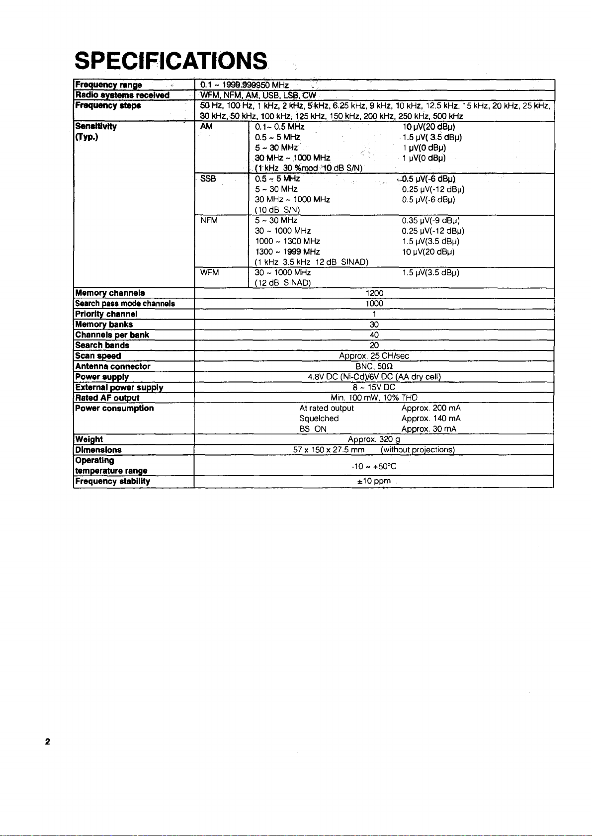
S P E C I F I C A T I O N S
Frequency range
Radio systems received
Frequency steps
Sensitivity
CTYP-)
Memory channels
Search pass mode channels
Priority channel 1
Memory banks
Channels per bank 40
Search bands
Scan speed Approx. 25 CH/sec
Antenna connector
Power supply
External power supply
Rated AF output
Power consumption At rated output Approx. 200 mA
Weight
Dimensions
Operating
temperature range
Frequency stability
0.1 - 1999.999950 MHz .
WFM, NFM, AM, USB, LSB.CW
50 Hz, 100 Hz, 1 kHz, 2 kHz, 5*Hz, 6.25 kHz, 9 kHz, 10 kHz, 12.5 kHz, 15 kHz, 20 kHz, 25 kHz,
30 kHz, 50 kHz, 100 kHz, 125 kHz, 150 kHz, 200 kHz. 250 kHz, 500 kHz
AM
SSB
NFM
WFM
0.1-0.5 MHz 10pV(20dBp)
0.5 - 5 MHz 1.5 pV( 3.5 dBp)
5 - 3 0 MHz 1 pV(0 dBp)
30 M Hz- .1000 MHz 1 pV(0 dBp)
(1 kHz 30 %mod *10 dB S/N)
0 .5 -5 MHz , -.0.5 pV(-6 dBp)
5 -3 0 MHz 0.25 |jV(-12 dB|j)
30 MHz ~ 1000 MHz 0.5 pV(-6 dBp)
(10 dB S/N)
5 -3 0 MHz 0.35 pV(-9 dBp)
30 - 1000 MHz 0.25 pV(-12 dBp)
1000 - 1300 MHz 1.5 pV(3.5 dBp)
1300 - 1999 MHz 10 pV(20 dBp)
(1 kHz 3.5 kHz 12 dB SINAD)
30 - 1000 MHz 1.5 pV(3.5 dBp)
(12 dB SINAD)
1200
1000
30
20
BNC, 50il
4.8V DC (Ni-Cd)/6V DC (AA dry cell)
8 - 15V DC
Min. 100 mW, 10% THD
Squelched Approx. 140 mA
BS ON Approx. 30 mA
Approx. 320 g
57 x 150 x 27.5 mm (without projections)
-10 - +50°C
±10 ppm
Page 3
C I R C U I T D E S C R IP T I O N
1) Frequency
• Signals in the 0.1 - 449.99 MH z and 1500 ~ 2000 MHz bands are converted into the 736.25 MHz first IF
signal by the first local oscillator signal.
• Signals in the 450 ~ 1499.99 M Hz band are converted into the 275.45 MHz first IF signal by this same
first local oscillator signal.
• The first IF signal is converted into the 45.05 MHz second IF signal from the two second local oscillator
signals (671.2 and 230.4 MHz) by the second mixer circuit.
• Depending on the mode, the second IF signal is input to one of the two IF amplifier ICs. In one mode,
the second IF signal is mixed with a 34.35 M Hz third local oscillator signal and converted into a third IF
signal of 10.7 MHz, while in the other, it is mixed with a 44.595 MHz third local oscillator signal and
converted into the third IF signal of 455 kHz.
2) Receiver Block
Front-End Circuit
• The received signal from the antenna goes through the antenna circuits (D128, D124 and D125) and is
screened by seven band pass filters consisting of several antenna switches (D131, D111, D127, D112,
D126, D114, D 130, D115, D134, D119, D135, D121, D136, D122 and D133) to remove unwanted
signals.
•T he RF signal is amplified by each of the RF amplifiers Q123 (0.1 - 222 MH z), Q 125 (222 ~ 797 M Hz),
Q12 6 (797 ~ 2000 MHz) and Q118. It is then converted into the first IF signal by the first mixer circuit
(T101, T100, D109 and D 1 16).
• The adjacent signals in first IF signal, the 275.45 M Hz IF signal and the 736.25 MHz IF signal are filtered
out respectively by the band switch (D110 and D102), the IF filter (L113, L110, L107 and L101) and the
IF filter (FL102 and FL101). Then, the signals are input into the second mixer circuit (Q102).
• In the second mixer circuit, the 12.8 M Hz reference signal is mixed with either a 230.4 MHz second local
oscillator signal (amplified 18 times) or a 691. 2 MHz second local oscillator signal (amplified 54 times)
selected by a switch (D101), and is converted into a 45.05 MHz second IF signal.
• In the W FM mode, the second IF signal goes through an IF filter (L301) and is input into pin No. 16 of an
IF IC (IC305). A 10.7 M Hz third IF signal converted by the IC’s internal mixer is output from pin No. 14,
filtered of adjacent signals by a ceramic filter (FL302) and input into pin No. 12. Next, it is demodulated
by IC’s internal limiter amplifier and quadrature detection circuit, and output from pin No. 8 as an AF
signal.
Page 4
• In the NFM, AM, SSB and C W modes, the second IF signal goes through an IF filter (XF300 and XF301)
and is input to pin No. 16 of an IF IC (IC304). A 455 kHz third IF signal converted by the IC ’s internal
mixer is output from pin No. 3 and is filtered of adjacent signals by a ceramic filter (FL301). Thereafter, a
switch (D 30 6 and D309) selects the m ode. In the NFM m ode, the signal is input to pin No. 5,
demodulated by IC ’s internal limiter amplifier and quadrature detection circuit, and output from pin No. 9
as an AF signal. In the AM mode, the signal is amplified by an AGC amplifier (Q313) and input to pin No.
7 of an IF IC (IC305). It is amplified inside the circuit, demodulated by the detection circuit and output
from pin No. 8 as an AF signal. In the SSB mode, the signal goes through a ceramic filter (FL303) and is
amplified by an AGC amplifier (Q313) and an IF amplifier (Q316). It is then mixed with a carrier signal,
which is generated by the BFO circuit (X302 and Q318) and fed through a buffer (Q317), demodulated
by a balanced modulation circuit consisting of diodes (Q315, D314 and D313), and output as an AF
signal.
• The AF signal for each of the modes is selected with a switch (IC308) and amplified by an AF signal
amplifier (IC309). It is controlled by an AF mute circuit (Q 319) and adjusted for volume by an electronic
volume (IC306). It is then amplified by an audio amplifier (IC307) and input to the speaker.
3) PLL Synthesizer Circuit
•T h e signal from a 12.8 M Hz crystal (X100) oscillator circuit (Q 100) is input to a PLL IC (IC101) to obtain
a 10 MH z reference oscillation signal frequency. The comparison frequency is output from a VCO circuit
(Q 114, L108, D104, D105, D107 and D108), amplified by an amplifier (Q115, Q 113 and Q 116) and
divided by a divider inside the PLL IC. It is then compared against the reference frequency to make the
PLL synthesizer.
•T he V CO output signal (675 ~ 1225 MHz) is amplified by a buffer amplifier (Q115, Q 1 13 and Q120) and
input into the first mixer as the first local oscillator signal.
• Frequencies of 9 kHz steps or less are varied by the VCX O circuit (X300, D 304 and D305) of the D/A
converter (IC303).
Page 5
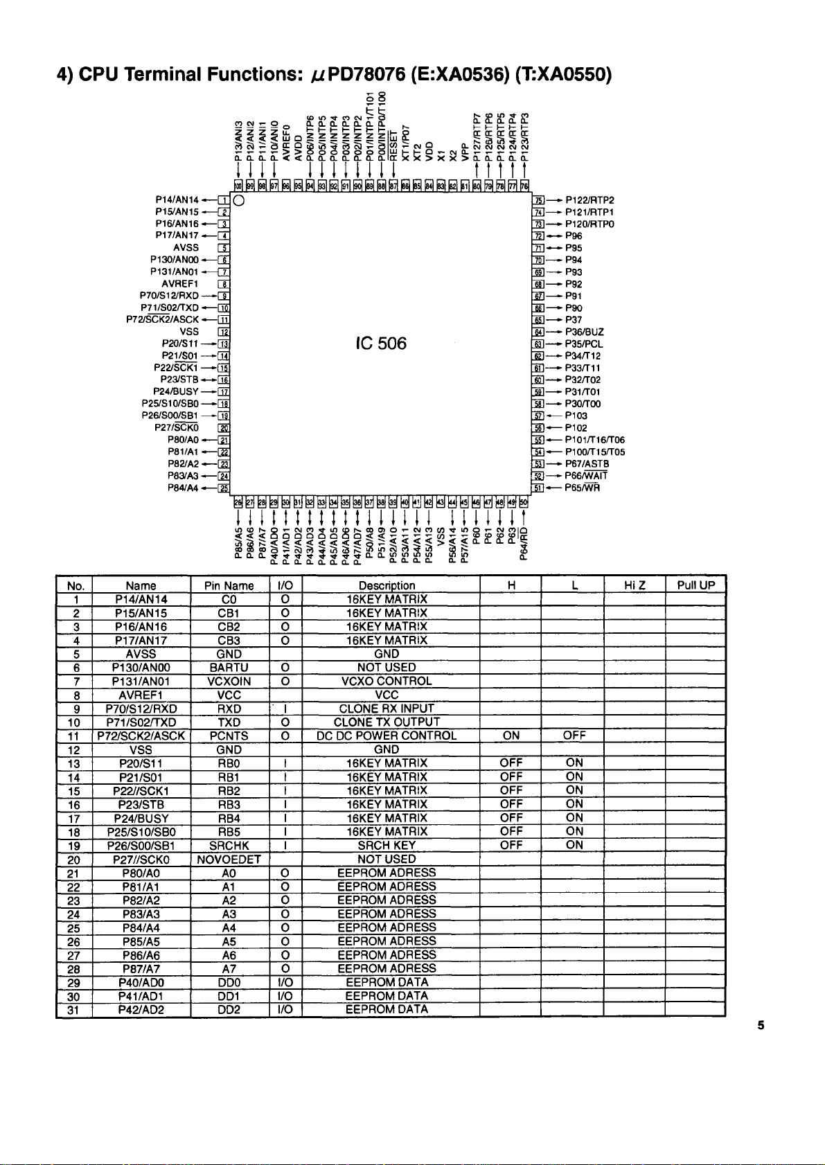
4) CPU Terminal Functions: /iPD78076 (E:XA0536) (T:XA0550)
o 8
o _ Û. 0. CL CL Q. Û. Q.
5 ? t— H H h* h- H h-
< < <
c\l •«-
^->> 00 00 000
CL<<(LCLCLQ_CLÜ-CL
CD ir> Tf co cm ^ o
ts£
CO ^ CM û
œ5<5<>><S>Q.Q.Ü.Q.Q.
n. çp in m
CL O. CL CL CL
H H I- I- H
Œ Œ <r Œ Œ
K <3 ÎÎ5 ^ C»5
Q- CM CM CM CM CM
Û. 1- 1- r- f- f-
P1 4 /AN 1 4 — [ i
P15 /AN15 «— E
P16 /AN16 •*— Œ
P17 /AN 1 7 - — ( T
AVSS E
P130/A N0 0 — Œ 70] — - P94
P1 31/AN01 -— (T
AVR E F1 CE
P70/S12/R XD — CL
P71/S02/TXD — Q ï
P72 /SC K 2 /ASC K — Q ï
O
vs s nz S ] — ► P36/BU Z
P2 0/S 11 —- Q I
P21/S01 — - E
P22/SCK1 — Q I
P23 /ST B — Q I 1 ] — P3 2/T02
P24/B US Y — Qz
P25/S 1 0 /SB 0 — Q I
P2 6/S 00/SB1 — Q I
P2 7 /S C K 0 S
P8 0 /A 0 — m 1 3 — P 101/T16/T06
P81/A1 -—E s a — P 100/T15 /T0 5
P82/A 2 » — [ S S I - P67 /A STB
P8 3/A 3 — |S
P8 4/A 4 •*—[ S 3 H — P 65/W R
U ) Ö S Q i- M < t) ^ m < Ü S # ® 0 ’-C M n W ^ W 0 i-C M «IQ
<<<ûûûû ûûûû<<^^^;w^^»® œ 5plS
cooBcoô^côcîî^îBtâî^^^c^cn^1« con. 3
Û-Û-Û-Û-Û-Û-Û-Û- Û. Û. Û. Û. Û. Û.
No.
1
Name Pin Name
P14/AN 14
CO
2 P15/AN 15 CB1
3
4
5
6
7 P131/AN01
8
9
10
11
12 VSS
13 P20/S11
14
15
16
17
18
19
20
21
22
23
24
25
26
27
28
29
30
31
P16/AN 16 CB2 0
P17/AN17
CB3 0
AVSS GND GND
P130/AN00
BARTU
VCXOIN O
AVREF1
VCC
P70/S12/RXD RXD ' I
P71/S02/TXD TXD O CLONE TX OUTPUT
P72/SCK2/ASCK
PCNTS 0
GND
RBO
P21/S01 RB1
P22//SCK1 RB2
P23/STB RB3
P24/BUSY RB4 I
P25/S10/SBO RB5
P26/S00/SB1 SRCHK
P27//SCK0
P80/A0
P81/A1
NOVOEDET
AO
A1 0
P82/A2 A2
P83/A3
A3 0
P84/A4 A4 0
P85/A5
P86/A6
A5 0
A6 0
P87/A7 A7 0
P40/AD0 DDO I/O
P41/AD1 DD1 I/O
P42/AD2
DD2 I/O
I/O
0 16KEY MATRIX
0 16KEY MATRIX
16KEY MATRIX
16KEY MATRIX
0
VCXO CONTROL
CLONE RX INPUT
DC DC POWER CONTROL
I
16KEY MATRIX
I 16KEY MATRIX
I
16KEY MATRIX
I 16KEY MATRIX
16KEY MATRIX
I
16KEY MATRIX
I SRCH KEY
0
EEPROM ADRESS
EEPROM ADRESS
0 EEPROM ADRESS
EEPROM ADRESS
EEPROM ADRESS
EEPROM ADRESS
EEPROM ADRESS
EEPROM ADRESS
EEPROM DATA
EEPROM DATA
EEPROM DATA
IC 506
Description H
NOT USED
VCC
GND
OFF ON
OFF ON
OFF
OFF
OFF ON
OFF
OFF ON
NOT USED
S — P122/RTP 2
Ï D - P1 21/RTP1
3 ] — P1 2 0/R TP0
2 ] - — P9 6
ID —— P 95
1 0 — ► P93
M l— - P92
S I — - P91
a — - P9o
S I — - P37
S ] — ► P35 /P C L
S I— ► P 34/T12
ID — P 3 3 /T11
M l - P 31/T01
I D - P 30/T00
E l — P103
sa-— pi o2
S ] — P66/W A IT
L HiZ
ON OFF
ON
ON
ON
Pull UP
5
Page 6
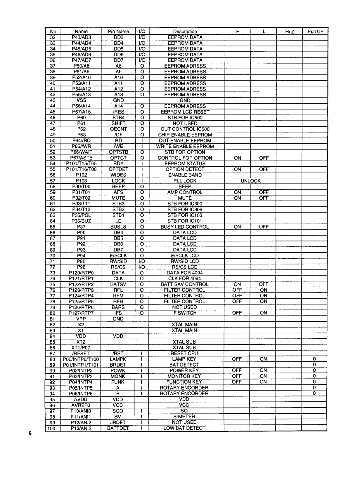
No. Name Pin Name
32 P43/AD3 DD3
33
34
35 P46/AD6 DD6 I/O
36
37 P50/A8 A8
38 P51/A9 A9
39 P52/A10 A10 O
40 P53/A11 A11
41
42
43
44
45 P57/A15
46 P60
47 P61
48 P62
49
50 P64//RD RD I OUT ENABLE EEPROM
51
52
53 P67/ASTB OPTCT
54
55 P101/T16/T06 OPTDET I OPTION DETECT
56 P102 WIDES I
57 P103 LOCK I PLLLOCK UNLOCK
58 P30/T00 BEEP
59 P31/T01 AFS
60 P32/T02 MUTE
61
62 P34/T12 STB2
63 P35/PCL
64 P36/BUZ
65 P37 BUSLS 0 BUSY LED CONTROL
66
67
68 P92 DB6 o DATA LCD
69 P93
70
71 P95 RW/SID I/O RW/SID LCD
72 P96 RS/CS I/O
73 P120/RTP0
74 P121/RTP1
75
76 P123/RTP3
77
78 P125/RTP5
79 P126/RTP6
80
81
82 X2
83
84 VDD VDD
85 XT2
86 XT1/P07
87
88
89 P01/INTP1/T101
90
91 P03/INTP3
92 P04/INTP4 FUNK
93 P05/INTP5
94
95
96
97
98
99
100
P44/AD4 DD4
P45/AD5 DD5 I/O EEPROM DATA
P47/AD7 DD7 I/O EEPROM DATA
P54/A12 A12 O EEPROM ADRESS
P55/A13 A13 O EEPROM ADRESS
VSS GND
P56/A14
P63
P65//WR
P66/WAIT
P100/T15/T05 RDY I EEPROM STATUS
P33/T11
P90
P91 DB5 0
P94 E/SCLK 0 E/SCLK LCD
P122/RTP2 BATSV
P124/RTP4
P127/RTP7
VPP GND
X1 XTAL MAIN
/RESET
POO/INTPO/T100 LAMPK
P02/INTP2 POWK
P06/INTP6
AVDD VDD
AVREFO
P10/ANI0
P11/ANI1
P12/ANI2
P13/ANI3
A14 O EEPROM ADRESS
/RES O EEPROM LCD RESET
STB4 O
SHIFT
OECNT O OUT CONTROL IC500
/CE
/WE I
OPTSTB 0 STB FOR OPTION
STB3
STB1
LE 0 STB FOR IC101
DB4
DB7
DATA
CLK 0
RFL 0 FILTER CONTROL
RFM
RFH
BARS
IFS 0
/RST I RESET CPU
BRDET
MONK I MONITOR KEY
A I ROTARY ENCORDER
B I
VCC
SQD I
SM I
JRDET
BATTDET I
I/O
I/O
I/O
O EEPROM ADRESS
O
O EEPROM ADRESS
O NOT USED
0
0 CONTROL FOR OPTION ON OFF
0 BEEP
0
0
0 STB FOR IC300
0 STB FOR IC306
0 STB FOR IC103
0 DATA LCD
0
0
0
0 FILTER CONTROL
0 FILTER CONTROL
0
I LAMP KEY
I
I POWER KEY
I
I
Description H
EEPROM DATA
EEPROM DATA
EEPROM DATA
EEPROM ADRESS
EEPROM ADRESS
GND
STB FOR IC500
CHIP ENABLE EEPROM
WRITE ENABLE EEPROM
ENABLE BAND
AMP CONTROL
MUTE ON OFF
DATA LCD
DATA LCD
RS/CS LCD
DATA FOR 4094
CLK FOR 4094
BATT SAV CONTROL
NOT USED
IF SWITCH
XTAL MAIN
XTAL SUB
XTAL SUB
BAT DETECT
FUNCTION KEY
ROTARY ENCORDER
VDD
VCC
SO
S-METER
NOT USED
LOW BAT DETECT
ON OFF
ON OFF
ON OFF
ON OFF
OFF ON
OFF’ ON
OFF ON
OFF
OFF ON
OFF
OFF
OFF ON
L
ON
ON p
ON 0
HiZ
Pull UP
0
0
0
0
0
Page 7
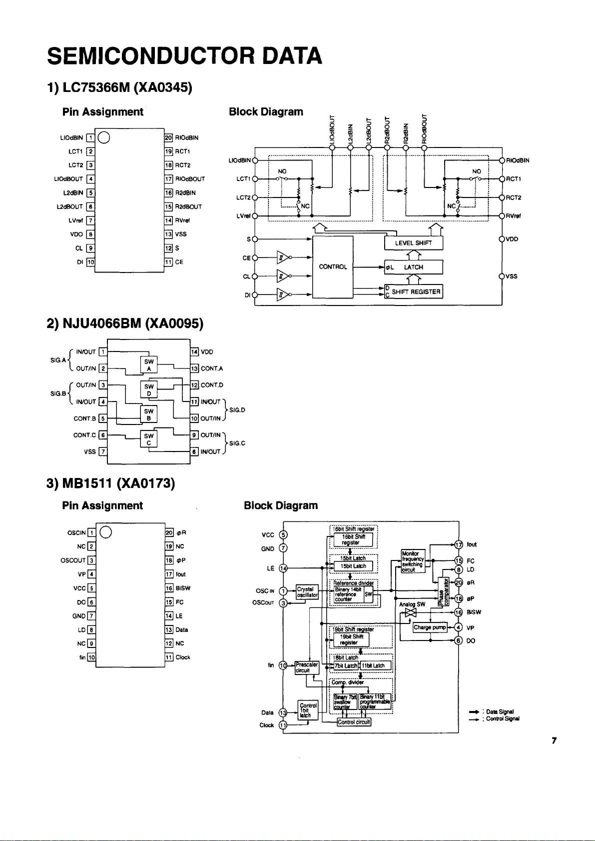
S E M I C O N D U C T O R D A T A
1) LC75366M (XA0345)
Pin Assignment
LIOdBIN [ 7
LIOdBOUT [T 17] RIOdBOUT
L2dBIN [5 16] R2dBIN
L2dBOUT [ T
0
LCT1 [2
LCT2 [ ? Tß] RCT2
LVref |T Ü ] RVrel
VDO [¥
CL ( J 32] S
DI [To TT] c e
20] RIOdBIN
19] RCT1
Ü R2dBOUT
13] VSS
2) NJU4066BM (XA0095)
SIQ.A
SIQ.B
ÏÏ] IN/OUT 'I
TÖ] OUT/IN J
9] OUT/IN 'j
T ] IN/OUT
Block Diagram
r
LIOdBIN Q
NO
LCT1 O
LC T 2 0
LVref Q
^•SJG.D
j-SIG.C
- o > o -
S O
C E O
C L Q
l NC
K
8
■o
0
<) -
CONTROL
z
GO
T3
1-
D
s
-0 -
1-
z
0
CO
T3
8
CM
CM
Œ
cr
- O--0-
LEVEL SHIFT
z z n
0L LATCH
~ T F
. SHIFT REGISTER
1-
■>
0
§
0
1r
- O
NC >
NO
-o-fo -
RIOdBIN
ÖHCT 1
QRCT2
QRVref
QVDD
QVSS
3) MB1511 (XA0173)
Pin Assignment
OSCIN [T
o s c o u t |T
O
NC [?
v p | T
vc c|T Tê] Bisw
d o [ F
g n d |T
l d [ 7
n c [ ?
tin [To
20] 0 R
19] NC
ïj[] 0 P
17] fout
T5] FC
14] LE
13] Data
12] NC
ÏT| Clock
Block Diagram
VCC
GNO
LE
OSCiN
OSCouT
: Data Signal
; Control Signai
Page 8
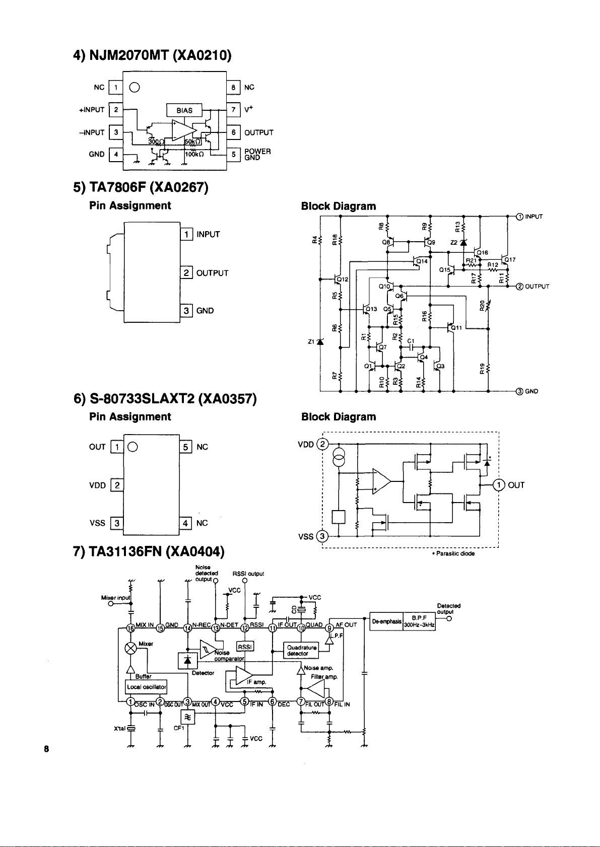
4) NJM207 0 M T (X A 0 2 10 )
5) TA7806F (XA0267)
Pin Assignment Block Diagram
6) S-80733SLAXT2 (XA0357)
Pin Assignment Block Diagram
7) TA31136FN (XA0404)
detected RSSI output
Page 9
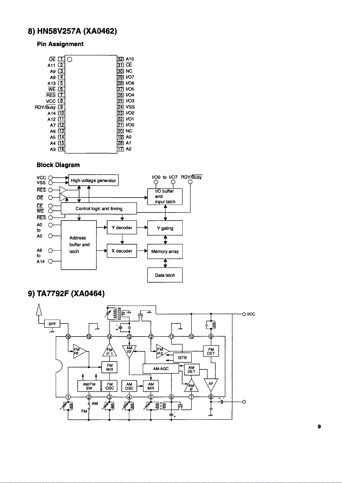
8) HN58V 2 5 7A (X A 04 62 )
Pin Assignment
OE ü
A11 GE
A13 SI
WE E
RES IX
VCC QT
RDY/Busy tH
A14 QS
A12 QI
O
A9 DE
A8 EE
A7 Q2 52 i/oo
A6 Q3
A5 IS
A4 QI
A3 (31
Block Diagram
m aio
in ce
30] NC
m i/o7
55] 1/06
57] 1/05
m 1/04
IS 1/03
Sä VSS
53] 1/02
52] 1/01
5Ü] NC
T51 AO
551 A1
T7] A2
9) TA7792F (XA0464)
9
Page 10
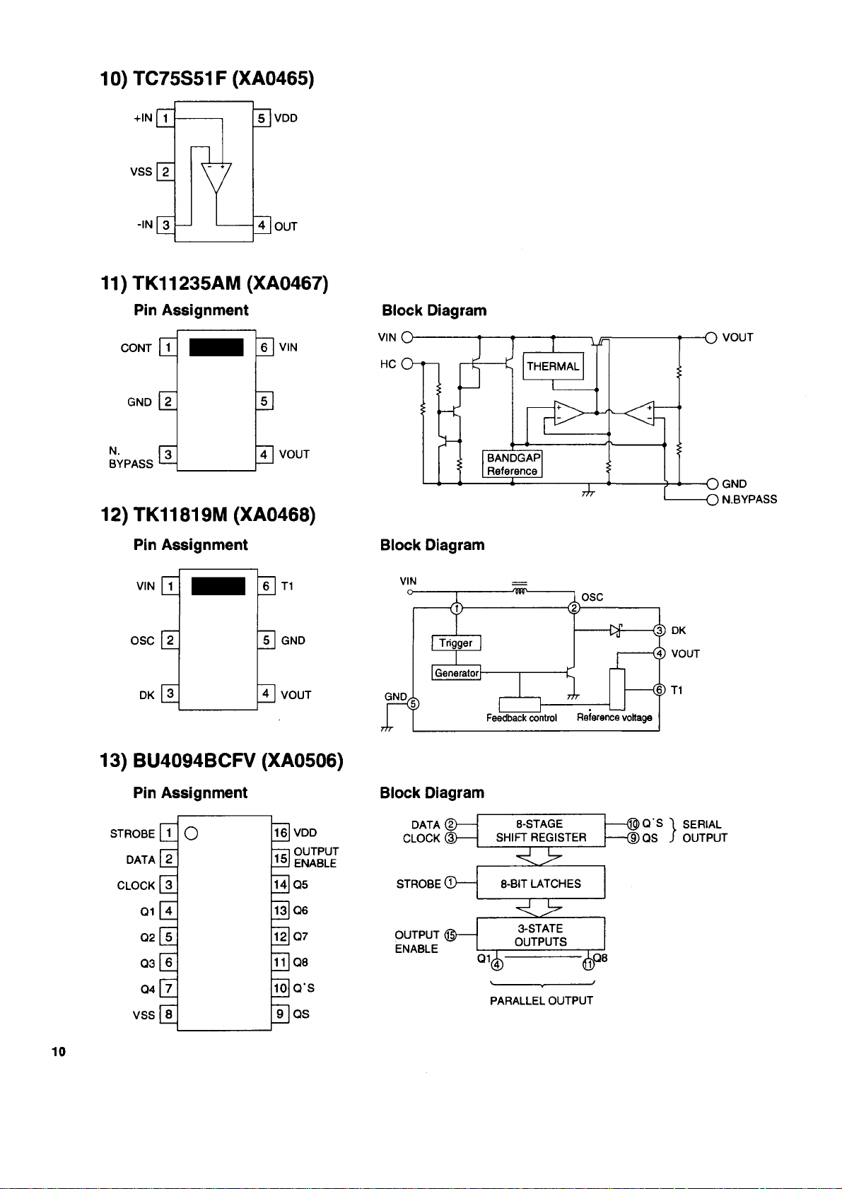
10) TC75S 5 1F (XA 0 4 6 5)
+IN 1
VSS 2
-IN 3
5 VDD
4 OUT
11) TK11235AM (XA0467)
Pin Assignment Block Diagram
12) TK11819M (XA0468)
Pin Assignment
VIN 1
OSC 2
DK 3
6 T1
5 GND
4 VOUT
13) BU4094BCFV (XA0506)
Pin Assignment
VDD
STROBE
DATA
CLOCK
Q1
Q2
Q3
o
16
15
14
13
12
11
OUTPUT
ENABLE
Q5
Q6
Q7
Q8
Block Diagram
VIN
Block Diagram
DATA (2)
CLOCK ©
STROBE ©
OUTPUT ©
ENABLE
-----
-----
-----
-----
8-STAGE
SHIFT REGISTER
8-BIT LATCHES
3-STATE
OUTPUTS
Q1
-----
©Q 'S "I SERIAL
-----
d)QS J OUTPUT
Q4
VSS 8
10
9 QS
Q S
PARALLEL OUTPUT
Page 11
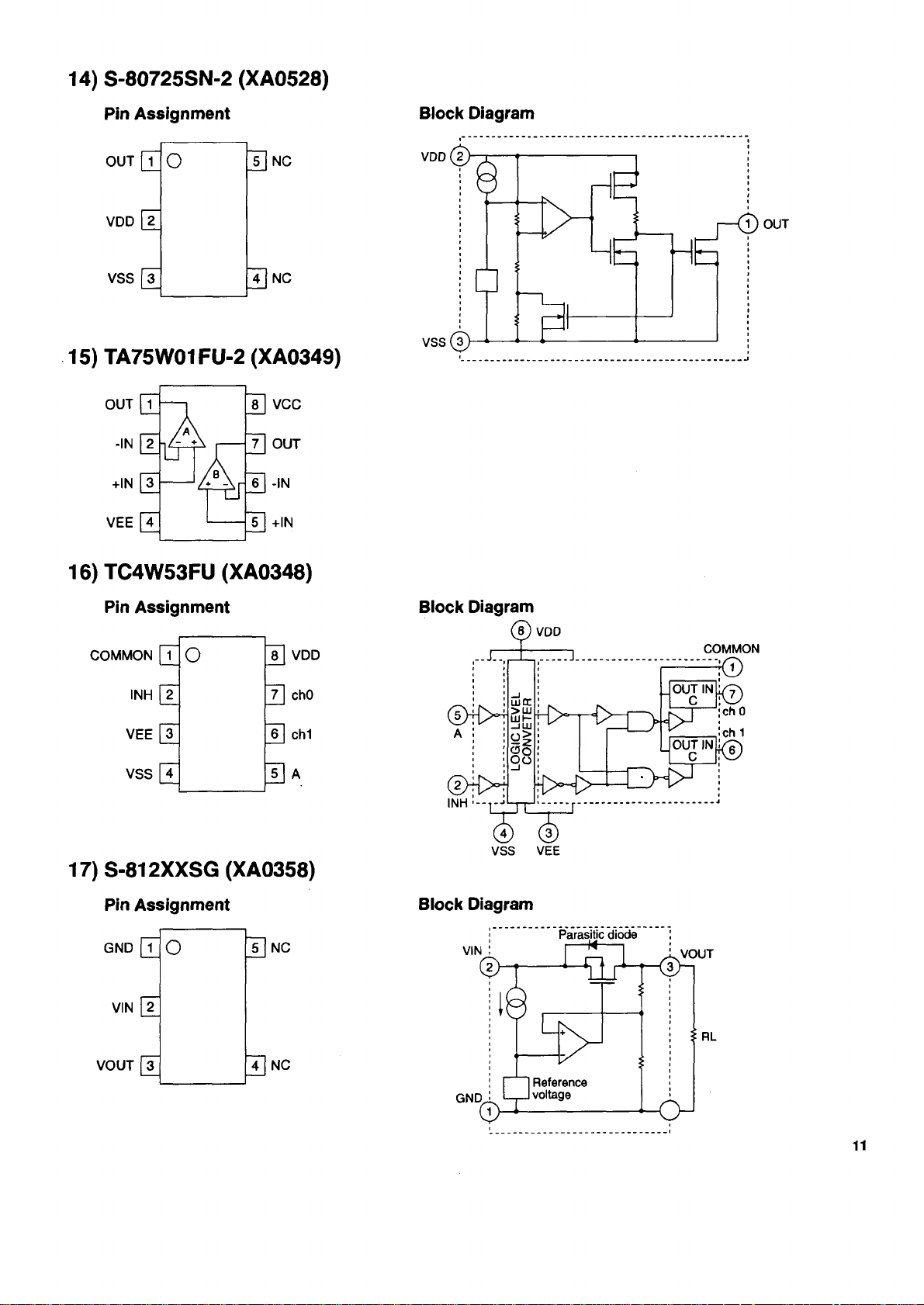
14) S-80725SN-2 (XA0528)
Pin Assignment
OUT 1
VDD 2
VSS 3
o
5 NC
4 NC
15) TA75W01FU-2 (XA0349)
OUT
-IN
Block Diagram
16) TC4W53FU (XA0348)
Pin Assignment
COMMON [T
INH
VEE
VSS
o
2 7
3
4 5
VDD
8
chO
6
ch1
A
17) S-812XXSG (XA0358)
Pin Assignment
GND
VIN 2
o
NC
Block Diagram
Block Diagram
VOUT 3
4 NC
Page 12
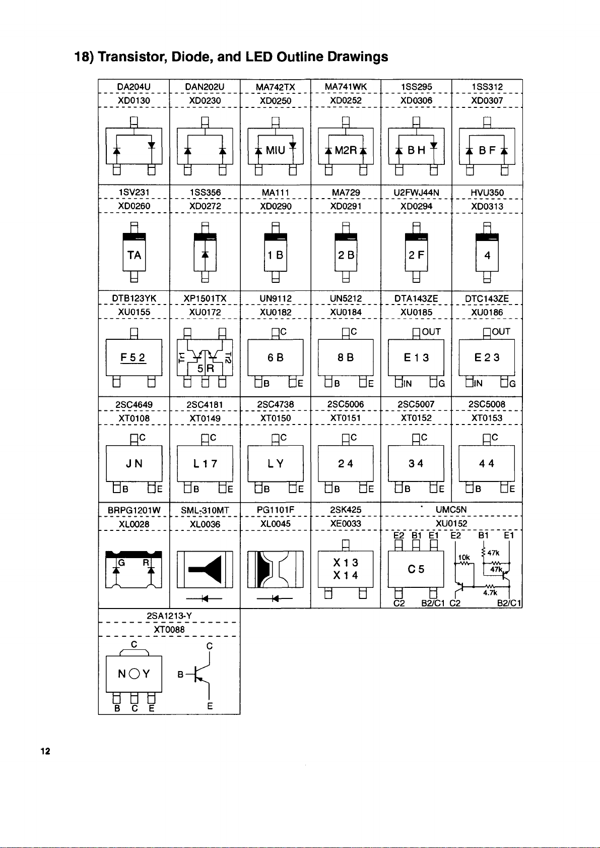
18) Transistor, Diode, and LED Outline Drawings
DA204U
XD0130
DAN202U
XD0230
"d d
1SV231 1SS356
XD0260
XD0272
-
TA
■ff
DTB123YK
XU0155
XP1501TX
XU0172
MA742TX
XD0250
MA111
XD0290
A
1 B
UN9112
XU0182
MA741WK
XD0252
U f f
MA729
XD0291
A
2 B
u
UN5212
XU0184
1SS295
XD0306
U2FWJ44N
XD0294
A
2 F
f f
DTA143ZE
XU0185
1SS312
XD0307
d d
HVU350
XD0313
A
4
n
DTC143ZE
XU0186
□ OUT
2SC4649
XT0108
m .
J N
" E l i E f i
BRPG1201W
XL0028
2SA1213-Y
XT0088
d d d
2SC4181
XT0149
m .
L 1 7
f f i
SML:310MT
XL0036
2SC4738 2SC5006
XT0151
ne
LY
U b f f i
PG1101F
XL0045
m
2 4
dB B i
2SK425
XE0033
_ ff
X 1 3
X 1 4
H4-
f f f f
2SC5007
XT0152
m
3 4
Ü B Ü E
2SC5008
XT0153XT0150
m
4 4
L J B S i
UMC5N
XU0152
B C E
Page 13

19 ) L C D Di a g ra m
ii
LCD Center
l h -
TCP,SEAL Center
\ V -
ii
n
i •
9 M PMS VFO ® O B S
“ PRIO SKIP ¡ATT o-n-€II
I i m m i i i i i
m w w w
Page 14

E X P L O D E D V I E W
1) Front/Rear View
Parts No.
1
KZ0073Y
2
YZ0149 $
3 FG0236Y
4
AX0003
5 PR 00 340
?£YZ0149 is integrated
into 1.
Page 15

2) IF Uni t/ C P U Un i t
Parts No.
1
AF0020
2
UP0282
3 FM0100
4 FG0178Y
AP0004
5
TN006Z
6
7
UP0281
AX0002
8
FM0098
9
TL0017
10
DG0027
11
12 TL0020
TX0004
13
EL0037
14
TZ0064
15
16 AX0001
17 FG0218
ST0052
18
MKCLOOAA
19
20 MNCLH2AA
21 ES0011
22 FG0255
FG0180Y
23
FG0176Y
24
FG0235
25
FG0242
26
FG0243Y
27
FG0177Y
28
KZ0051Y
29
Page 16

3) Charge/RF Uni t
Parts No.
1
AK0001
2
AX0001
3 TS0141
4
AF0020
5 S D0045
SC0008A
6
7 FP0093A
TS0110
8
(T/E version only)
9 FP0094
10 NK0042Y
11 FG0181Y
12 AN0012Y
13
UE0193AZ
14 FM0112
15 KB0064Y
A
Page 17

i i ü ü ü l ü
S g
l i l l l l l l l l l l i l l l l l l l l l l l i l l l l l l l l l l l l l i l i
...............................
111 S S1 1 SS I11 1 1 11
i l i i i i i i i i i i l i l l l ü l l i l l i l I I H I i i i l l i i i i i i i i i l l l l l i i i i l i l i l l i l I I i l i i l i
ï l i i s i l P i i i i
s î s s ;
lü U O Ü U Ü X X X K X X X S k Œ Œ Œ
P A R T S L IS T
i S S X S S (o t
S S iliS isgoa a a
üsss.
l i i
Page 18

00
FM. No. Parts No.
C3Ú0 CU0104 C2012JB1E104M
0301 C$0213 TMCMA1A225MTR
C302
C303
C304 CS0068
C305 CU3035
0306
0307
C308 CU3059
C309 CU3069 C1608JF1E104ZTA
0310
0311
0313
0315 CS0216
C316
C317
0318
0319
0320
0321
0322
0325 CU3105 C1608UJ1H180JT-A\
0326
0327 CU3047 C1608JB1H103KTA
0328 CU3047 C1608JB1H103KTA
0329
0330 CU3059
0333 CU3059
0334
0335
0336 CU3113
0337 CU3023 C1608CH1H101JTA
0338
0339 CU3016
0340
0341 CU3047
0342 CU3016
0343 CU3047
0344 CU0103
0345 CU3101
0346
0347
0348 CU3006 C1608CH1H050CTA
0349
C350
0351
0352
C353
0354
0355
C356 CU3116
0358 CU3016 C1608CH1H270JTA
C359 CU3047 C1608JB1H103KTA
C360 CU305A C1606JF1E104ZTA
0361
0362 CSQ213
0363
0364
0365
0366 CU3059 C1608JF1E104ZTA
0367
C368
0369
C370
0371
0372
0373 CU3069
0374
0375 CS0213
0376 CU3059 C1608JF1E104ZTA
0377 CU3059
0378 CU3059 C1606JF1E104ZTA
C379 CU3059
0380 CS0063 TMCSA1V104MTR
0361 CU3069
0382 CU3069
0383 CS0063
0384
0385 CU3043 01608JB1H472KTA
0386
0387
TZ0049 Silicon dumper
CS0213
CU3047 C1608JB1H103KTA
CS0213 TMCMA1A225MTR
CU3114 EMK107BJ105ZA-T
CU0104 C2012JB1E104M
CU3059
CU3059 C1608JF1E104ZTA
CU3047 C1608JB1H103KTA
CU0104
OS0369
CU3047 C1608JB1H103KTA
CU3047 C1608JB1H103KTA
CU30C5 C1608CH1H040CTA
CS0213
CU3047 C1606JB1H103KTAX
CU3047
CU3047
CU3047
CU3017
CU3015
CU3047 C1608JB1H103KTA
CU3059
CU3107
CU3027 C1608CH1H221JTA
CU3027
CU3111 C1608JB1 Cl 04M
CU3035
CU3035 C1608JB1H102KT A
CU3047 C1608JB1H103KT A
CU3035 C1606J61H102KTA
CU 3012 C1608CH1H120JTA
CU3115 C1608RH1H101JT-A
CU3047 C1608JB1H103KTA
CU3047
CU3047 C1606JB1H103KTA
CU3027 C1608CH1H221JTA
CU3035 C1608JB1H102KTA
CU3031 C1608JB1H471KTA
CU3047 C1608JB1H103KTA
CS0382
0U3021 C1608CH1H660JTA
CU3051
CU3059 C160BJF1E104ZTA
IFUnit
TMCMA1A225MTR
TMCSC1E475MTR
C1606JB1H102KTA
C1608JF1E104ZTA
C1608JF1E104ZTA
TMCMB1A106MTR
C2012JB1E104M
TMCMO0J107MTR
TMCMA1A225MTR
C1606JB1H103KTA
C1608JF1E104ZTA
C1608JF1E104ZTA
C1608JB1H103KTA
C1608JB1H103KTA
C1608CH1H910JTA
C1608CH1H330JTA
C1608CH1H270JTA
C1608CH1H220JTA
C1606JB1H103KTA
C1608CH1H270JTA
C1608JB1H103KT A
C2012JF1C105ZT-N
C1608JB1C473KTA
C1606JF1E1042TA
C1608UJ1H820JT-A
C1608CH1H221JTA
C1608JB1H102KTA
C1608CH1H471KT-A
TMCMA1A225MTR
C1608JB1H103KTA
C1606JF1E104ZTA
TMCMB1A226MTR
TMCWA1A225MTR
C1606JF1E104ZTA
C1606JF1E104ZTA
C1608JF1E104ZTA
C1606JF1E104ZTA
TMCSA1V104UTR
C1606JB1E223KTA
Parts Name
Ver.
Ref.No. Parts No Parts Name
0388 CÜ3059 Ciè06JPiEi042TA
0389
C390
0391
0392
0393
C394
0395
0396
0397 CU3047
0398
C399
C400 CS0213 TMCMA1A225MTR
C401 CS0213 TMCMA1A225MTR
0402
0403 CU3043
0404
0405 CU3033
C407 CU3047
0408 CS0213 TMCMA1A225MTR
C409 CS0213
0410
0411 CU3047
0413
0414
C415
0416 CS0213
C417
0418
0419
0420
0421 CU3023 C1608CH1H101JTA
0422 CS0213 TMCMA1A225MTR
0425
0426 CU0103 C2012JF1C105ZT-N
C427
0428
0429
0430 CS0369 TMCMD0J107MTR
0431 CU3111 C1608JB1C104M
0433
0436
C437 CU3047
CN301 UE0240 AXN440C530P
CN302 UE0308 IL-WX-10SB-VF
D300 X00290
0301
D302
D303
D304
D305 XD0313 HVU350TRF
D306 XD0230 DAN202U T106
D307
D308
D309
D310 X00250 MA742TX
D311
D313
D314
FL301
FL302
FL303 XC0025
10300 XA0506
IC301
IC303 XA0465 TC75S51 F(TE8SL)
IC304
IC306
IC306 XA0345 LC75366M-TLM
10307
10308
IC309
10310
IC311 XA0348
10312 XA034S
JK300
JK301 UJ0019 HSJ1493-01-010
U01 QC0522
L303
L304 OH0005
L305 QH0006 KE-07727
L306 000507 LK16081R0K-T
1307 QH0002
L309
CU3059 C1606JF1E104ZTA
CU3059
CU3059
CU3023
CU3059
CU3059 C1608JF1E104ZTA
CU3059 C1606JF1E104ZTA
CU3035
CU3114
CU3023 C1608CH1H101JTA
CU3047
CU3035 CJW8JSJH1Û2KTA
CU3114
CS0216 ■ TMCMB1A106MTR
CU3059
CU3047 C1608J61H103KTA
CS0213 TMCMA1A225MTR
CU3114
CS0213 TMCMA1A225MTR
CU3047 C1608JB1H103KTA
CU3047
CU30J1
CU3047
CS0213
CU3059 C1608JF1E104ZTA
CU3114
XD0307
X00250
XD0252 MA741WKTX
XD0313
XD0272 1SS356 TW11
XD0250 MA742TX
X00230
XD0250 MA742TX
XD0250 MA742TX
X00250
XC0024
XC0037 •
XAM67
XA0404
XA0464
XA0210 NJM2070M TI
XA0095 NJU4066BMT1
XAM65 TC75S51 F(TE85L)
XAQ349
UJ0022
QC0506
QH0004
C1G08JF1E104ZTA
C1606JF1E1Û42TA
C1608CH1H101JTA
C1608JF1E104ZTA
C1606JB1H102KTA
01608JB1H103KTA
EMK107BJ105ZA-T
C160BJB1H103KTA
01608JB1H472KTA
C1606JB1H681KTA
C1608J61H103KTA
TMCMA1A225MTR
EMK107BJ105ZA-T
C1608JB1H1Q3KTA
C1608JF1E104ZTA
TMCMA1A225MTR
EMK107BJ105ZA-T
Cl 608JBIH103KTA
C1508CHIH100CTA
C1608JB1H103KTA
TMCMA1A225MTR
EMK107BJ105ZA-T
C1608JB1H103KTA
MA111-TX
1SS312(TE85L)
MA742TX
HVU350TRF
DAN202U T106
MA742 TX
CFWM455F
SFE10.7MJA
CFWM455I
BU4094BCFV-E2
TK11235AMTL
TA31136FN(EL)
TA7792F(TP1)
TA75W01FU(TE12L)
TC4W53FU(TE12)
TC4W53FU(TE12)
HSJ1102-01-540
LÛH1N1R5JÛ4
LK1608R56K-T
KE-07725
KE-07731
KE-07724-1
Y
Page 19

n Ref. No. Parts No.
Q300
0301 XU0186
0302 XE0033
0303 XU0186
0304
Q305
0306
0307
0306 XU0185
0309 XT0106
0310 XT0106
0311 XT0106
0312 XT0106
0313 XT0106
0314
0315 XT0150
0316 XT0150
0317
0318 XT0106
0319 XT0150
0320 XU0184
R300
R301 RK3053
R302 RK3043
R304 RK3052 ERJ3GSYJ153V R392
R305 RK3056 ERJ3GSYJ333V R393 RK3034 ERJ3GSYJ471V
R306 RK3056
R307
R308 RK3062
R309
R310
R311
R312 RK3062 ERJ3GSYJ104V R401 RK3061 ERJ3GSYJ823V
R316 RK30S8
R317 RK3047 ERJ3GSYJ562V
0318
R319
R320 RK3038
R321 RK3038 ERJ3GSYJ102V R408
R322 RK3039
R323 RK3053
R324 RK3050 ERJ3GSYJ103V
R325 RK3026
R326
R327 RK3067 ERJ3GSYJ274V R414
R328 RK3036
R330 RK3070 ERJ3GSYJ474V
R331 RK3035
R332 RK3048
R333 RK3040 ERJ3GSYJ152V R421
R334 RK3026 ERJ3GSYJ101V
R335
R336 RK3001 ERJ3GSYOROOV R425
R337 RK3051 ERJ3GSYJ123V
R338
R339
R340
R341 RK3031
R342 RK3026 ERJ3GSYJ101V
R343 RK3048
R344
R34S RK3054 ERJ3GSYJ223V
R346 RK3054 ERJ3GSYJ223V
R347 RK3054 ERJ3GSYJ223V
R346
R349 RK3001 ERJ3GSY0R00V R444
R350
R351
R352
R353
R354 RK3054 ERJ3GSYJ223V
R355
R356 RK3048 ERJ3GSYJ682V
R357 RK3026 ERJ3GSYJ101V
R358 RK3050 ERJ3GSYJ103V
R359 RK3031 ERJ3GSYJ271V
R360
R361 RK3046
R362
R363
R364
R365 RK3059 ERJ3GSYJ563V
R366 RK3022 ERJ3GSYJ470V
XU0172
XT0150 2SC4738(TE85L)
XT0066
XU018S 0TA143ZEATI R373
XU0185
XT0150 2SC4738(TE85L)
XT0108
RK0114 ERJ6GEYJ1R0V
RK3026
RK3048
RK3046
RK3047 ERJ36SYJ562V
RK3038
RK3039
RK30S2 ERJ3GSYJ153V
RK3040 ERJ3GSYJ152V R424
RK30S8 ERJ3GSYJ473V R427 RK3059
RK30S8 ERJ3GSYJ473V R426 RK3050
RK3039
RK3051
RK3014 ERJ3GSYJ100V
RK3064
RK30S0
RK3042 ERJ3GSYJ222V R447
RK3044 ERJ3GSYJ332V
RK3052 ERJ3GSYJ153V
RK3059 ERJ3GSYJ563V
RK3032
RK3034 ERJ3GSYJ471V
RK3022 ERJ3GSYJ470V
Parts Ñama
XP1501-TX R367 RK30?1
DTC143ZEATL
2SK425-T1B X13 X14 R369 RK3034
0TC143ZEATL R370
2SA1213YTE12R R372
0TA143ZEATI
0TA143ZEATI R375 RK3054
2SC4649-TLN
2SC4649*TLN R377
2SC4649*TLN
2SC4649-TLN R379 RK3040 ERJ3GSYJ152V
2SC4649-TLN R380
2SC4738<TE85L) R382 RK3054 ERJ3GSYJ223V
2SC4738(TE85L) R363 RK3001 ERJ3GSYOROOV
2SC4649-TLN
2SC4649-TIN
2SC4738(TE85L) R386
UN5212-(TX)
ERJ3GSYJ183V
ERJ3GSYJ272V
ERJ3GSYJ473V R394
ERJ3GSYJ101V
ERJ3GSYJ104V R396
ERJ3GSYJ682V R397
ERJ3GSYJ472V
ERJ3GSYJ473V
ERJ3GSYJ102V
ERJ3GSYJ122V
ERJ3GSYJ102V R407
ERJ3GSYJ122V
ERJ3GSYJ183V
ERJ3GSYJ101V R412
ERJ3GSYJ102V R417
ERJ3GSYJ561V
ERJ3GSYJ682V
ERJ3GSYJ122V
ERJ3GSYJ271V
ERJ3GSYJ682V
ERJ3GSYJ123V R437
ERJ3GSYJ154V
ERJ3GSYJ103V
ERJ3GSYJ682V
ERJ3GSYJ331V
Ver.
Ref. No.
R368
R371
R374
R376 RK3031
R378
R381
R384
R38S
R388 RK3034
R389
R390
R391
R395
R399 RK3034 ERJ3GSYJ471V
R400 RK3034
R402 RK3054 ERJ3GSYJ223V
R403 RK3054 ERJ3GSYJ223V
R405
R406
R409
R410 RK3001 ERJ3GSYOROOV
R411
R413
R418 RK3034 ERJ3GSYJ471V
R419
R420
R423 RK3074 ERJ3GSYJ105V
R426 RK3030 ERJ3GSYJ221V
R432 RK3062 ERJ3GSYJ104V
R434 RK3062
R435 RK3056 ERJ3GSYJ473V
R436 RK3050 ERJ3GSYJ103V
R438
R439 RK3001 ERJ3GSY0R00V T
R442
R443 RK3054
R445 RK3001
R446 RK3001 ERJ3GSY0R00V
R446
R449 RK3038 ERJ3GSYJ102V
R499 RK3050
TC300
VR300 RH0142
VR301 RH0146 MVR22HXBRN473
VR302 RH0146
VR303
VR304 RH0142
X300 XQ0095 UM-S 44.595MHz
X301 XQ0094
X302
XF300 XF0029
XF301 XF0029
Parts No. Parts Ñame
RK3022
RK3Q26
RK3054
RK3026
RK3001
RK3049
RK3038
RK3062
RK3001
RK3022
RK3038
RK3038
RK3038
RK3026
RK30S9
RK3030
RK3034
RK3026
RK30S9
RK3059
RK3026
RK3038
RK3074
RK3038 ERJ3GSYJ102V
RK3050
RK30S1
RK3001 ERJ3GSY0R00V
RK3030
RK3062
RK3050
RK3030
RK3050
RK3050
RK3074 ERJ3GSYJ105V
RK3034 ERJ3GSYJ471V
RK3046
RK3050 ERJ3GSYJ103V
RK3014
RK3054 ERJ3GSYJ223V
RK3001
RK3001
RK3030 ERJ3GSYJ221V
CT0034
RH0144
XC0027
ERJ3GSYÓR00V
ERJ3GSYJ470V
ERJ3GSYJ471V
ERJ3GSYJ101V
ERJ3GSYJ223V
ERJ3GSYJ101V
ERJ3GSY0R00V
ERJ3GSYJ822V
ERJ3GSYJ223V
ERJ3GSYJ271V
ERJ3GSYJ102V
ERJ3GSYJ104V
ERJ3GSYOROOV
ERJ3GSYJ470V
ERJ3GSYJ102V
ERJ3GSYJ102V
ERJ3GSYJ102V
ERJ3GSYJ471V
ERJ3GSYJ101V
ERJ3GSYJ563V
ERJ3GSYJ221V
ERJ3GSYJ471V
ERJ3GSYJ101V
ERJ3GSYJ563V
ERJ3GSYJ563V
ERJ3GSYJ101V
ERJ3GSYJ471V
ERJ3GSYJ102V
ERJ3GSYJ105V
ERJ3GSYJ103V
ERJ3GSYJ123V
ERJ3GSYJ221V
ERJ3GSYJ475V
ERJ3GSYJ103V
ERJ3GSYJ221V
ERJ3GSYJ103V
ERJ3GSYJ103V
ERJ3GSYJ472V
ERJ3GSYJ563V
ERJ3GSYJ103V
ERJ3GSYJ104V
ERJ3GSYJ100V
ERJ3GSYJ223V
ERJ3GSY0R00V
ERJ3GSY0R00V
ERJ3GSY0R00V
ERJ3GSYJ103V
CTZ3S-30CW1-P
MVR22HXBRN103
MVR22HXBRN473
MVR22HXBRN223
MVR22HXBRN103
UM-5 34.35MHz
CSK455J
45M3065F(45.055MHz)
45M3065F(45.055MHz)
Ver.
Page 20

S s e g g s § § § g ig g g g g g § e a S S s i8 is iS llli!IiI!iI
^ I lilllë B illliîg lillS lî I Ig l^ iS I Ü S à llia iS Ig s is s s s s I H S S â is s S S e s g iâ g S S iiS
5 5 5 5 5 5 5 5 5 5
i ü ü ü i
¡ ¡ ¡ ¡ ¡ ¡ ¡ ¡ ¡ ¡ l l l l í í l l l l l í l l l l l l l l l l l l l l l i l í l l l l l l l l l l i l l l l l f l l l l í í l l l l l l l
r l I I I I
I! ï i
lisáass§a¿
I f l l l l l l l l ü l l l í i l i l i í l i i l l i i l l
Page 21

oo co
¡8
a i
R i l I I i I i i i i i ! ! I I ! i ! I l i ! I I ! ! l l i l ! i l i l i l l ! f I I i i i i S i i i l i i i i i i l i i l i i ü i i i g g l ï
i li ä i ä ä i ä ä
? ^ g y j t S y g B H ¿ H O fjO w O O
J s a S§ 1 s g I s § g te i te S t> te „ _
é é s á 5 Íd d Í5 d § §5 Íͧ § § iÍ3 ͧ 5 § § § 5 § lii5 lI§5 ͧ Íͧ § ͧ IÍ^^^ ^ as aa « s
3 - ç ç3 çç ç55 5^ eç e e j s ç ç f i
______
_
i i i i l i l i l i l i l i l l i
loo i l l l l i l l i l l i l l l i l l l l i i
a§ § l § § 5 5 i i l l 5 5 g ^ § m § l ! l § l § g § § ^ § ! l ^ ll g ^ l g s g ll i I i l i! l ! I I ! ! ll i I I I I i ll li il
Page 22

A D J U S T M E N T
1) Required measuring instruments and tools
1. Digital voltmeter
2. Regulated power supply of 10 V, 1 A or more
3. Oscilloscope
4. Frequency counter
5. External speaker
6. 0.1 M H z - 2 GH z SG
7. Audio analyzer
Level meter, distortion factor meter, linear detector
8. Spectrum analyzer
1 m coaxial cable with BNC connector
Speaker cable with 3.50 plug
f t 1 — 1
AF GND
Cloning cable with 2.5o stereo plug on both ends
NC CLONE GND
Power supply cable for external power supply terminal (For DJG5)
2) Adjustment
All SSG outputs are indicated in EMF.
The SP is 8 £2. Output is 50 mW.
Level meter filter must be H PF (30 - 50 Hz) and LPF ( 1 0 - 1 5 kHz).
Page 23

■ Power supply 10 V
After connecting and turning ON the power supply:
Turn the BS OFF.
Transfer adjustment data by cloning.
■ Frequency adjustment
Encircled numbers correspond to memory Nos. in the memory AO bank.
1. PLL reference frequency
• While receiving on f=198.70(NFM © ), using the frequency counter, measure TP104 in the RF Unit and
adjust TC 100 to obtain 934.95MHz ±1 k H z.
2. VCXO frequency
• While receiving on f=198.70(step=100H z, NFM © ), using the frequency counter, measure TP304 in the IF
Unit, and adjust VR303 and V R300 to obtain 44.595 M Hz ±20 0H z.
• When receiving on f=198.701 MH z © , adjust to 44.60 49M H z±2 00H z.
• Switch © 198.700 M Hz and © 198.7001 M Hz and set amplitude to 9.9 kHz from VR303. Adjust to 44.5950
MHz when at 198.700 M Hz from VR300.
3. SSB BFO frequency
•W h ile receiving on f=198.70(USB © ), using the frequency counter, measure T P308 in the IF Unit and
adjust TC 300 to obtain 456.0kHz +200Hz / -600Hz.
4. PLL lock check
• Check that voltage is 8 ~ 15 V using the digital voltmeter on f=300.0(NFM @ ) and measuring TP103 in the
RF Unit.
• Check that voltage is in 3 - 25 V using the digital voltmeter on f=449.940(NFM © ) and measuring T P103 in
the RF Unit.
5. Local level adjustment
• Connect the spectrum analyzer to antenna connector.
Set to maximum value while receiving on f=198.70 © and adjusting L103, L105, L106, and FL100 in the RF
Unit.
6. NFM distortion
• Apply SG=60dBu 1 kHz. Measure SP terminal. Adjust L307 in the IF Unit.
While receiving on f= 198.70, using the distortion factor meter and oscilloscope, set distortion factor to
minimum before making other adjustments, and set max. AF output to 6%.
• When receiving on 3.5kH z DEV (N FM © ), always turn adjustment core of L307 counter-clockwise. Be
careful not to crack the core when turning clockwise.
Page 24

7. NFM sensitivity
•A pply SG=6dBu 1kHz and 3.5kHz DEV (NFM © ) . Measure SP terminal. Adjust FI102, FL101, and L102 in
the RF Unit.
While receiving on f=198.70, using the distortion factor meter oscilloscope, repeat adjustment until obtaining
optimum SINAD.
•A pply SG=0dBu 1kHz and 3.5kH z D EV(NFM ® ). Measure SP terminal. Adjust L113, L110, L107, and
L101 in the RF Unit.
While receiving on f=510.03, using the distortion factor meter oscilloscope, repeat adjustment until obtaining
optimum SINAD.
8. WFM distortion
• Apply SG=60dBu 1kHz and 22.5kHz DEV(WFM ® ). Measure SP terminal. Adjust L305 in the IF Unit.
While receiving on f=198.7, using the distortion factor meter oscilloscope, set distortion factor to minimum
and max. AF output to 6% .
9. WFM sensitivity
• Apply SG=10dB u 1 kHz and 22.5kHz D EV(W FM ® ) . Measure SP terminal. Adjust L304 and L309 in the IF
Unit.
While receiving on f=198.70, using the distortion factor meter oscilloscope, repeat adjustment until obtaining
optimum SINAD.
10. SQ level adjustment
• Apply SG=-3dBu. Measure SP BUSY terminal. Adjust VR302 in the IF Unit.
While receiving on f=198.70(N FM ® ), adjust on LCD SQ level 1, turn VR 304 clockwise to close squelch.
Then, turn counter-clockwise to open and fix. However, close with SQ.
11. NFM S meter adjustment
• Apply SG=25dBu, unmodulated(NFM (D). Measure LCD terminal. Adjust VR302 in the IF Unit.
While receiving on f=198.70, turn SG OFF when S meter is full scale. Check S meter does not light up.
12. WFM S meter adjustment
• Apply SG=32dBu, unmodulated ® , WFM . Measure LCD terminal. Adjust VR301 in the IF Unit.
While receiving on f=198.70, turn SG OFF when S meter is full scale. Check S meter does not light up.
Page 25

P C B O A R D V I E W
C P U Un it Side A
J j swsiau
C 503
o
SV511
o
o
0511
pnq
i t }
5 3
C
Bf
“ 'V
Jl
SW5B0
f8e
V □
O
o
R551
C332QZD
cs s ïED
C555 (TED
C334ŒZD
R3390
C5Ï0HD
C5Í4ÍFT1
C555 ÜZD
Oi
D O
C558ED
C53/ED
C5 56E D
C55e
E D
C559
ED
Ç337 IJVJ] E D C361
JC558
E D
E D
C540
SI
E3JC544
EDC545
EDC545
a r
tfl {
® V
a> V m
□
5)
o
0500 O501
0
D D B D $ O Q 0 Q Q O
0502
(O
3 3
0505
Q ]
24
Page 26

CPU Unit Side B
CiUc*»
QR57I
UJra^g g
o
o
10508
o
[EDC530
o o
25
Page 27

RF Unit Side A
CP 100
IO
a
C210
IO
SH RS 8 F$R
e U U s 5 B P SFl
cu
-j
_í
—-
in.
..
a
♦
z n < Q
t u
J t
r r m ΠH 1
LED C219
C215
QZD
C214
-|fU
3a
0151 PI 55 D1Î6
9 I Í Í O ’ Ö 0
4 Up 0 1 3 0 rn m 0155
a - 4 D o , = . 0
caseaZD 0126 G3iC25^
C249LLiD
<c-
L 1 2 5
■£255fFT1 JQ
■
-j
N.
CU
0)
fU
Il »’II
0227<UIO
«J
0 1 1 6
3
□
3
ZD
dp
3
(X
□
tn
LmmJ
LanaJ
C231
fU
in
ßmtmm,
10
ED
-J
C 2 3 0
C 1 9 9
11 »11
0119,
!Q k
R20511 II ru ]£ N B
8 s S S
" BB Q
C9
h-
II » 1IC1B6
fT^TlLlll
¡Q c , P ñ a » ' » 7
cieflZD Qi is QZD ciee
R160O ÍM jB s
Or
S r-jr D u
C l+4 Cl 48
11° II I M l
(I II U ll
RT42 RT45
o
Hi 43 n
A ñ fl ib °
a o
f i h l s r a I
LI 03
TC100
in
S 1
I o
R123
iia
Cl 48
0 1 0 9
R150 R155
o o
n~ °Tici51
Û o » . .
0*151
Cl 50
w
TP 1 0 0
26
Page 28

RF Unit Side B
Q 1 5 4
AJ
CC C
1
Cg 40
11° II n n R224
q Í )
R B
I I J ) r S 5 7
Q R 2 3 8
Rgggim
C2320ZÖ
ñ?
(VJ
tt
e q
C 2 5 9
RaP
f t
Q131
O
R 2 S 5
C 2 2 8
II«It
:225[T°TI
0128
4 ir >
D J 2 5
’Ql3
|$ra icgsi
0£ »
Q 3
0 1 2 4
0 1 3 0
f t
10)
R228
o to
C247
II » II
2 2
ivi w
(j oc
(S.—.
m
R2170 in
R2161Í II
II ° 11
C 2 42
rm R 2i4
E Ü C 2 0 9
Ö
0153 Rg08fm
R g lg d II II» ||C 2 05
R e n rm
Q126
O ” 87
11 11
RFTC
C 2 0 3Q Z D
O
R 2 0 9
a *
D120
C N 1 0 0
fiO
CD
ö
Q 1 1 9
It ° P
C 182 o
a»
i " l
.7 8
o
1.1» ll
C 1 8 1
0110
— a
tn r
0112
II
«-
Cl 59
R135
Cl38 E D
Cl 36ir°Tl
a ®
R 1 3 6 0
R157 fT~n
C1401HD
®
a *-4
_ u
a ►-*
133 Cl 37
Q102
R 1 1 3 0
R u s o
C 2 7 1 ÍF T 1
o n
o76e y
0EDC135
_____
in
C C
o DouPi - y
Cl 14
fl»11
_ l a ^
e i ¿ / " t o a w ® j o ,a 0 . a
O t o O Z D R is e fts O R is e n - n ^ p
8B08ia® O ? 117
D118C 3 h 5 F i
R ioorm S D n l r >
C176ÍFT1 Ä 72lO F
C177HZD 0V 8 O 1=
C178EED QZDr i74
I!0 U O kR
d Z I j « 1 7 6 r i
tHDci80 | s
Q
R 177
C156Í1 ?J1
Cl 5511133
II0II
Cl 54
3 ^
1 <0
J 0J
3 U
C153
n*Ti
Bs ft®
0r3ii Q>05
O
R131
H C 1 5 2 iT 7 n
“ 2 EDciízg
n n L
Cl 33
ll » II
_
0110
1in
3 C C.
\
N io in co
tr J <r o
|C192
« » » O , u ,
ftj w w
n - n l86[°!
[ O r 190
Q Í2 3
^ "cTsTdHI ED tnR181
ö ^ 6 8 C163ED ^
QU7 FIS R162° 0U3 DfP.
_ R I 6 3 0
Q J 1 p _ < o R 1 8 1
Cl 71
U U 2E D «
CM5ff3l£y 2
D * "ä SQ Qj§
Qs
O r h 6
|C 147
^ £12? 012)
S O (0 1
¡B
R103O 0 8 t o
1100OÄD ED c 0
R101O 0101
C 186
m b D s
“ C l 85
0 0120
E 1 C 1 8 4
EDc^r
QZDR157
or
£Z
@23
o ^ ö
rrjT]fu “ » (RD
u— u r . 0 2 0 T T 1 9
jllfi.ll IHJ R, m
o
C102ÜZD
27
Page 29

R38l|Q Œ33 c587
8 0 l g Us
f ~ \ pEB
A I
TP307 R584
è ñ £
TP303
M (vj ^ r
TP508 J fc
■ S K R H flñ ñ R f l ñ i U L g
, e h ic 508 V ) rar
R406Í1 H
iO R4^
yyyyyyyyy dlO
n—ri TP306 ( > ^ 0 3 1 8
™ ‘ TP505y J4 R374 W ? ....
m K j g Ü 3
C374
C348
n « n ti ° n C356
gf=l IHDC35iO R 3 55
SS ^ C55¿ 3]H353
J ^ f C Í EB « *»
E f e « « tEDC357
Rin f i ] OR552
Sri o
R333
R301O
DDD B S ^ - ^
s l i K a u e . i b ¡
n=, 3 p STB F
iLÜ
TP300 f â l TP501 O
VRÎ00
R3U
Page 30

IF Unit Side B
11 »'fl C433
1111
IC312
lo
TTTT
rSS
'K
30
K)|
ILJU1 Ü JSk
to I—~1
UTTU
ï B
ÍU no
frHR455
Q520
(U
K) q: u
K> J±, ,—,
U bl C4£0(FT1a
O R « i iñ p c c
>404
„ s S S g d g
Sr I I S
h * d B Ê b q
C405[I » II
GT“
ju y y Q3i7 u
v i a qxoqtî n m 55 ^ f í
R398QZD
C398 ED
C384
11 flR577
G
na
0310
glBBO
« I s * r,l7 U 3 E
j£R357 o: a C354 Ufc ^
D ) ED C553
00
S ñ B S o l r-n
in
ED z
C359 H| IC304
0>
ED
C381
R3761
O
N.
K)
U
0309
^ R 3 4 7 Í1 il
n.0309
" U » o R3e8
5Q > 5 |i5 a
0305
____
D304G)3 hd (TTn ?!
o
»55811 II ¡8 C328 £
° I C 3 0 2
R315
c
c
c
“ EDC314
k rrnR5i3
a:
« - ^
5 ; O
R422Ü TI
I423n— n R421
R42 5
□ to q
0
(xbd cd __
n j s ^ u__y C3
R394 0
R593fl f| 051^Tl 0 R388
a 0314
Q»«<
__
w t f b B |
£?ara,4EQ 0ZDr387
J5S5 a E l g
R372 ED
to
N. C
K> I
OC [
1 ü ® n
03
l û - sQ
3 R3
fl_Q,
“ S - S L5^ n
0300
IS.
K)
-R307 0IIlCS7lñ@ U0311 C363
c c
P. E» i s
C543 CD
fl »11 ¡2
^
S ^ t E D
ÍEJJ „ ®
R 3 4 4
o
R543fm
EDC3£1
II » II
C324
»50.0
Q303 Ú ÚQ301
V U TT
C412
Il II
R416
ŒIDC410
0
3D313
rr
'ù[Ë31C 390
n_EL-
R382
S R365
I ^
K)
1 U
o
-----
C335
ED
C353
jl I ° II
39P~
y * I r
C 3 8 8 m
nx.io £ H3D5 «
Ife 0 “ S ® i flf
u[OR3e5c367 j-u jjjjj
w
■ °is
tn fo
C jz
T T O
EÜC340
tm R340£
O) —
»0 ▼
KÎ »O
u CC
R5S7ED
C320 0301
E , g ,
R3220
ù û û
Q3
W » Q 30 7
„ R305
a
a;
B am 0
m O "
0 3 0 0
U
= _
II » 11
C 3 1 9
0 3 0 0
m
R4I2
O
g
u
ir
R316
O
g a
T T T B
I
e n « *
ED
C407
J Z L
Q305
“onr
C317
Q 3 0 0
C300
29
Page 31

PTT SW Unit Side A
PTT SW Unit Side B
O
J J siwiV V.
[o ]
“v r V
ÍOJ
¿> ^
O
f í
CHARGE Unit Side A
o o o
TPW3 fc
°
CHARGE Unit Side B
3G
C803
BID
Page 32

BLOCK DIAGRAM
31
32
Page 33

C I R C U I T D IA G R A M
CPU Unit
33
34
Page 34

HN58V257
- AS
- AI 3
- /WE
- /RES
- yç ç
- RDY//BUSY
-AM
-A12
-A7
-A6
IC506
ID
CNl
h-
ID
CM
00
m
A10
32
A10
31 /CE \
/CE
36
NC
29
1/07
28 DD6 \
1/06
I
>
27
1/05
26
1/04
25 DD3 N
1/03
24 \
VSS
23 DD2
1/02
22
1/01
21 DD0 \
I/O0
29
NC
19 7
18
17
DD7
DD5 N
DD4 N
DD1, \
A1 \
A2 \
\
\
\
CN504
CFP0508-0201
CFP0508-0201 «« «
o •- o
Page 35

RF U nit
35
Page 36

IH I
-------------------------------
lílí:
35
36
Page 37

IF Unit
R439
X10 X10T
0 0
37
X10E X10K
NC NC
Page 38

Page 39

D801
DA204U
Page 40

77 77
in Q-
-<s> ©
-0 0 (S>
JK 801
HEC2781 —010 0 2 0
— o
777 7
--------
CHARGE Unit
C=3
 Loading...