

Page 1

DJ-S40T / E
Service Manual
CONTENTS
SPECIFICATIONS
1) GENERAL ................................................................ 2
2) TRANSMITTER ........................................................ 2
3) RECEIVER ............................................................... 2
CIRCUIT DESCRIPTION
1) Receiver system ....................................................... 3
2) Terminalmitter system ............................................... 4
3) PLL, VCO Circuit.......................................................4
4) M38224M6M ............................................................ 5
SEMICONDUCTOR DATA
1) M64082A (XA0543) .................................................. 7
2) NMJ2070MT1 (XA210) ............................................. 8
3) NJM2904V (XA0573)................................................ 8
4) NJM2902V-TE1 (XA0596) ........................................ 9
5) TA31136FN (XA0404)...............................................9
6) UPC2771T (XA0545).............................................. 10
7) CAT24WC16JITE13 (XA0855)................................ 10
8) S-816A30AMC (XA0848)........................................ 10
9) S-80827ALNP (XA0857)......................................... 11
10) MRF9745T1 (XE0034)............................................ 11
11) Transistor, Diode and LED Outline Drawings........... 12
12) LCD Connection ..................................................... 13
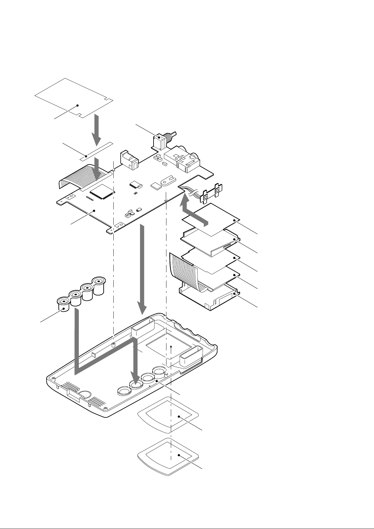
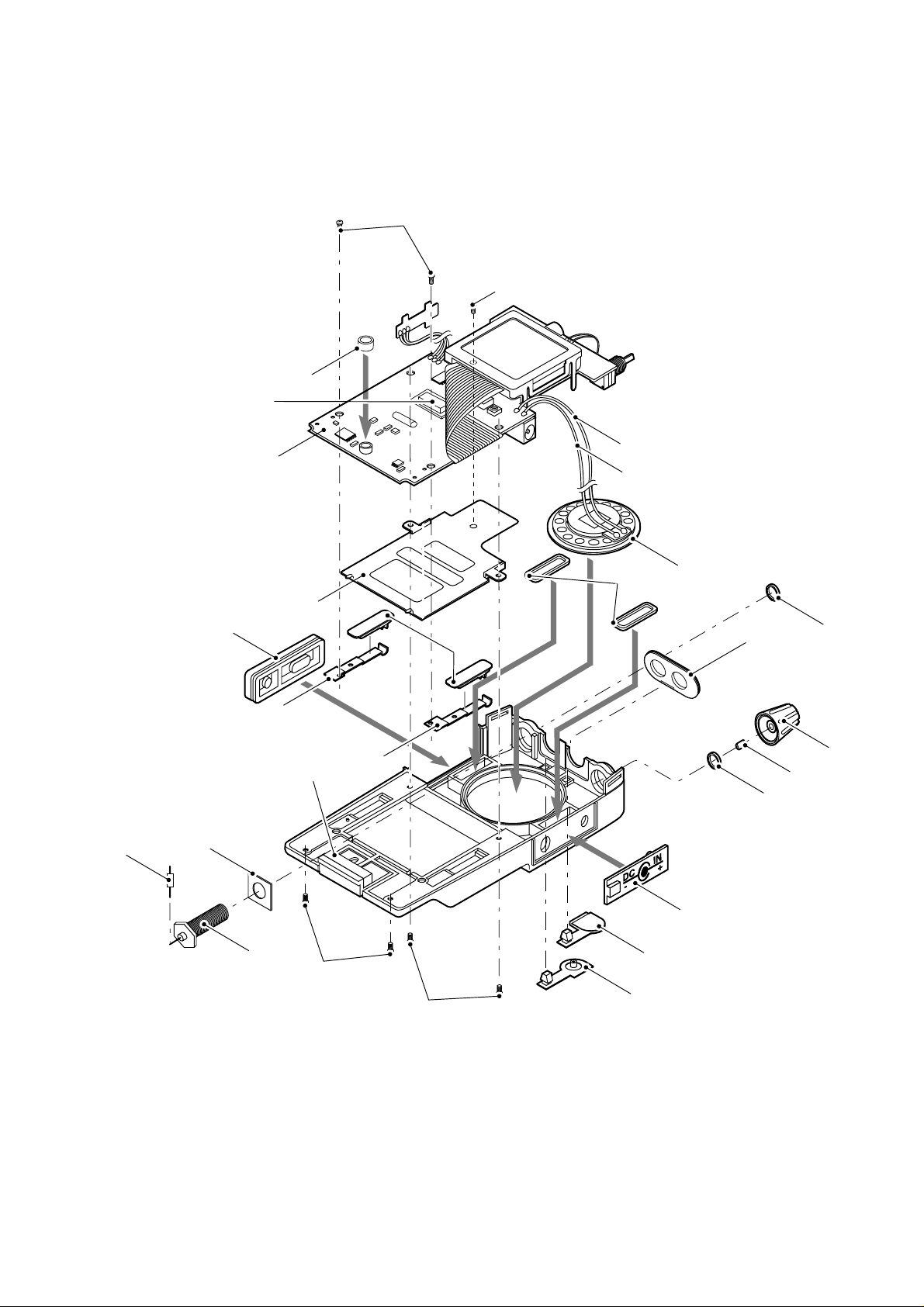
EXPLODED VIEW
1) Front V iew............................................................... 14
2) Bottom View............................................................15
PARTS LIST
MAIN Unit ......................................................... 16~20
SW Unit .................................................................. 20
Mechanical Parts .................................................... 20
Packing................................................................... 20
ADJUSTMENT ...................................................... 21~22
PC BOARD VIEW
1) UP0433(1/2) side A ................................................ 23
2) UP0433(1/2) side B ................................................ 24
3) PTT Unit WIRING ................................................... 25
SCHEMATIC DIAGRAM............................................. 26
BLOCK DIAGRAM...................................................... 27
ALINCO,INC.
Page 2

SPECIFICATIONS
1) GENERAL
Frequency coverage T : TX 430 ~ 449.995MHz RX 410 ~ 470MHz
E : TX 430 ~ 439.995MHz RX 430 ~ 439.995MHz
TA : TX 410 ~ 470MHz RX 410 ~ 470MHz
Mode F3E (FM)
Channel steps 5, 10, 12.5, 15, 20, 25, 30 & 50kHz
Memory channels 99 channels+1 CALL channel
Antenna connector SMA (50Ω unbalanced)
Frequency stability ±5 ppm
Microphone impedance 2kΩ nominal
Power supply 4.5 ~ 16.0V DC (EXT.ter monai)
3.6 ~ 16.0V DC (BATT ter minal)
Current 600mA (typical) Transmit high at 1W
150mA (typical) Receive at 280mW
40mA (typical) standby
15mA (typical) Battery save on
Usable temperature range -10 ~ +60° C (14 ~ 140°F)
Dimensions 56 (W) × 102 (H) × 30 (D) mm (with EDH-31)
2.2"(W) × 4.0"(H) × 1.18"(D) inches (with EDH-31)
(Projections not included)
Weight Approx. 160g (5.6oz) (with EBP-53N)
Approx. 95g (3.3oz) (without Battery)
Sub audible Tone(CTCSS) encoder/decoder installed (38tones)
2) TRANSMITTER
Output power Approx. 1.0W EBP-53N installed
Approx. 1.0W 13.8V DC
Approx. 0.6W EDH-31 installed
Approx. 0.2W (LOW)
Modulation system Variable reactance frequency modulation
Spurious emissions -60dB or less
Max. frequency deviation ±5kHz
3) RECEIVER
Receive system Double conversion superheterodyne
Intermediate frequencies 1st 21.7MHz / 2nd 450kHz
Sensitivity(12dB SINAD) -14.0µdB (0.2uV) or less [430 ~ 450MHz]
Selectivity -6dB : 12kHz or more
-60dB : 28kHz or less
Audio output power 280mW or higher( 8Ω load)
2
200mW (8Ω10% THD)
Page 3

CIRCUIT DESCRIPTION
1) Receiver System
The receiver system is a double superheterodyne system with a 21.7MHz first IF and
a 450kHz second IF.
1. Front End
The signal from the anntena is pssed through low-pass filter and input to RF coil L24
and L17(band pass filter).
The signal from L24 and L17 is amplified by Q9,Q10 and led to the band pass filter,
and let to the first mixer base of Q11.
2. First Mixer
The amplified signal (f0) by Q9,Q10 is mixed eith the first local oscillator signal(f0-21.7MHz)
from the PLL circuit by the first stage mixer Q11 and so is converted into the first IF signal.
The unwanted frequency band of the first IF signal is eliminated by the monolithic
crystal filter FL3,and led to IF amplifier Q8.
3. IF Circuit
The first IF signal is amplified by Q8, and input to pin 16 of IC3, where it is mixed withthe
second local oscillator signal(21.25MHz)and so is converted into the second IF signal(450kHz).
The second IF signal is output from pin3 of IC3, and unwanted frequency band of second IF
signal is eliminated by a ceramic filter FL2.
The resulting signal is then amplified by the second IF limiting amplifier, and detected
by quadrature circuit. the audio signal is output from pin9 of IC3
4.Audio Circuit
The demodulated signal in IF IC3 contains the audio signal and CTCSS signal .
CTCSS signal is passed through the low-pass filter of IC5 and led to TIN por t of CPU
to be decoded. The audio signal is input to the main volume VR3 passing through
de-emphasis circuit and high-pass filter circuit of Q19.The signal of which level is
adjusted at the main volume VR3 is input to IC6 of AF amp, then it is amplified to the
level that can drive the speaker.
5.Squelch Circuit
The noise in the audio signal from IC3 is passed through the noise-filter and input to pin8 of IC3.
IC3 includes filter amplifier,high-pass filter and rectifier.
The rectified voltage level from pin14 of IC3 is deliverd to the comparator of the CPU.
The voltage is led to pin1 of CPU and compared with the setting voltage.The squelch
will open if the input voltage is lower than the setting voltage.
During open squelch ,pin11(AFS)of CPU becomes”H”level and pin9(AFP)of CPU
becomes”L”level, AF control signal is being controlled and sounds is outputted from
the speaker.
3
Page 4

2)Transmitter System
1.Microphone Amplifier
The input signal from built-in or external microphone is led to the microphone mute
circuit Q15,pre-emphasis circuit ,IDC circuit IC4,the signal is input to the maximum
deviation adjustment volume VR2.Then mixed at the add VR2 with the CTCSS tone
signal which is generated by CPU,Then it is input to VCO as the modulation signal.
2.P o wer Amplifier
The signal from VCO is amplified by IC1 and then passed through the low-pass filter,
the antenna switch circuit and the output low-pass filter.
The unwanted harmonics frequency signal is eliminated by the low-pass filter and
input to the antenna.
3)PLL,VCO Circuit
Output frequency of PLL circuit is set by the serial data from microprocessor.
PLL circuit consists of VCO Q2,buffer amplifier Q6.
The pulse wave output of chage pump is converted to DC voltage by PLL loop filter
circuit,snd supplied to D2,D15 of varicap diode in VCO unit.
The frequency modulation is executed when audio signal voltage is supplied to the
varicap D3.
When PLL is unlocked,pin10 of IC2 goes to “High”.
4
Page 5
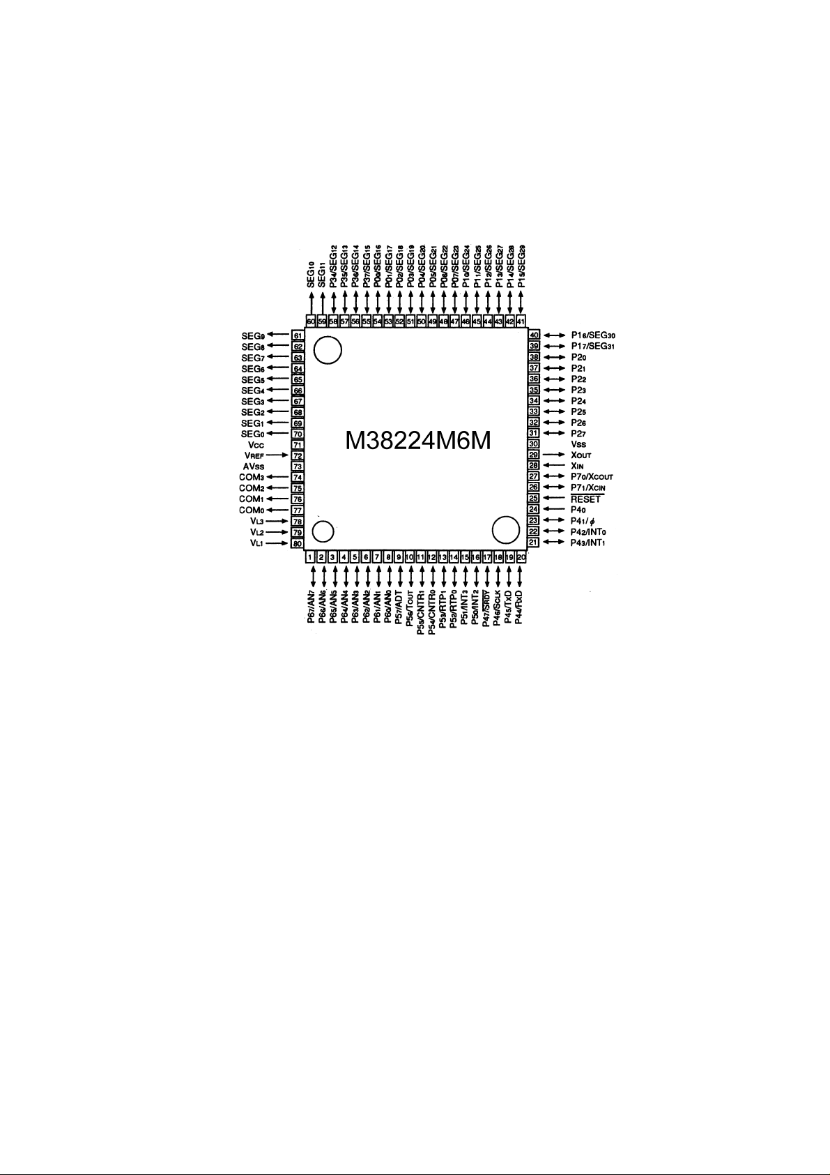
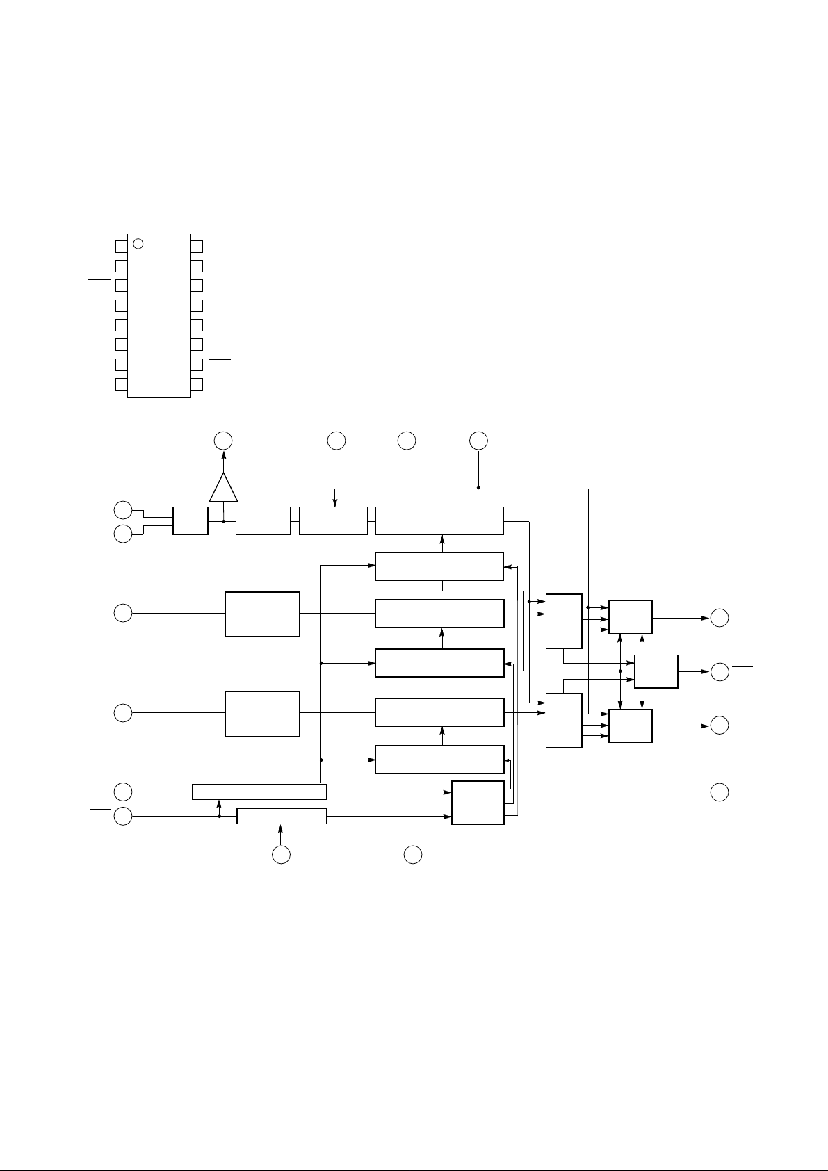
4) M38224M6M
CPU
Terminal Connection
(TOP VIEW)
5
Page 6
Terminal function of CPU
No. Pin Name Function I/O Logic
1 P67 SQL I A/D
2 P66 KEY I A/D
3 P65 VOX O Activ high
4 P64 EXTDC I A/D
5 P63 BP1 I A/D
6 P62 TIN I A/D
7 P61 SMT I A/D
8 P60 BATT I A/D
9 P57 AFP O Activ low
10 P56 BEEP I/O Pulse
11 P55 AFS O Activ high
12 CNTR0 TBST I/O Pulse
13 P53 BP3 I
14 P52 MONI I Activ low
15 P51 PSW I Activ low
16 P50 STB O Pulse
17 P47 DATA I/O Pulse
18 P46 CLK O Pulse
19 TxD CTX O Pulse
20 RxD CRX I Pulse
21 P43 SCR I Activ high
22 INTO BU I Activ low
23 P41 PTTK I Activ high
24 P40 BP4 I Activ high
25 RESET RESET I Activ low
26 P71 SCL O Pulse
27 P70 SDA I/O Pulse
28 Xin XIN I
29 Xout XOUT O
30 Vss GND
31 P27 MMUTE O Activ high
32 P26 H/L O Activ high
33 P25 EXP O Activ low
34 P24 FUNC I Activ low
35 P23 PTTC O Activ high
36 P22 P3C O Activ low
37 P21 C3C O Activ high
38 P20 R3C O Activ low
39 P17 T3C O Activ low
40 P16 TON4 O Activ high
Noise level input for squelch
Description
Key input ( , ,V/M)
Power cont.
Ext voltage input
Band plan 1
CTCSS tone input
S-meter input
Batt voltage input
Audio Amp ON/OFF
Beep sound out
Audio signal ON/OFF
Art tone output
Band plan 3
Monitor key input
Power switch input
Strobe for PLL
Data for PLL
Clock for PLL
UART data transmission output
UART data reception input
Alarm signal input
Back up signal detection input
PTT signal input
Band plan 4
Reset input
Serial clock for EEPRPM
Serial data for EEPRPM
CPU GND
Microphone mute output
Power control high=H
EXP terminal control
Func key input
Beep sound level control
Power supply control for VCO output
Power supply control
Power supply control for RX
Power supply control for TX
Tone output 4
No. Pin Name Function I/O Logic
41 P115 TON3 O Activ high
42 P14 TON2 O Activ high
43 P13 TON1 O Activ high
44 SEG26 SEG22 O
45 P115 SHIFT O Activ high
46 P10 LAMPC O Activ high
47 SEG23 SEG21 O
48 SEG22 SEG20 O
49 SEG21 SEG19 O
50 SEG20 SEG18 O
51 SEG19 SEG17 O
52 SEG18 SEG16 O
53 P01 CHG O Activ high
54 P00 MICC O Activ low
55 SEG15 SEG15 O
56 SEG14 SEG14 O
57 SEG13 SEG13 O
58 SEG12 SEG12 O
59 SEG11 SEG11 O
60 SEG10 SEG10 O
61 SEG9 SEG9 O
62 SEG8 SEG8 O
63 SEG7 SEG7 O
64 SEG6 SEG6 O
65 SEG5 SEG5 O
66 SEG4 SEG4 O
67 SEG3 SEG3 O
68 SEG2 SEG2 O
69 SEG1 SEG1 O
70 SEG0 SEG0 O
71 Vcc VDD
72 Vref VDD
73 Avss GND
74 COM3 COM3 O
75 COM2 COM2 O
76 COM1 COM1 O
77 COM0 COM0 O
78 VL3 VL3 I
79 VL2 VL2 I
80 VL1 VL1 I
Tone output 3
Description
Tone output 2
Tone output 1
LCD SEG 22
VCO shift output TX=H
Lamp ON/OFF output
LCD SEG 21
SEG 20
SEG 19
SEG 18
SEG 17
SEG 16
Battery charge control
TX mic amp power supply outout
SEG 15
SEG 14
SEG 13
SEG 12
SEG 11
SEG 10
SEG 9
SEG 8
SEG 7
SEG 6
SEG 5
SEG 4
SEG 3
SEG 2
SEG 1
SEG 0
LCD COM 3
LCD COM 2
LCD COM 1
LCD COM 0
LCD power supply
LCD power supply
LCD power supply
6
Page 7
SEMICONDUCTOR DATA
1) M64082AGP (XA0543)
DUAL PLL FREQUENCY SYNTHESIZER
XBo
CPS
RST
Vcc
Fin1
Vss
PD1
Xout
Xin
Fin2
1
SI
2
3
4
5
6
7
8
15
16
11
M64082AGP
16
Xin
15
Xout
14
GND
13
CONT
12
Vc1
11
Fin2
10
Lock
PD2
9
XBo
1 12 14 13
Buffer
OSC
1/2 divider
2-modulus
prescaler
(1/128, 1/129)
1/4 divider
through
for reference frequency
Data latch (11 or 17 bits)
GNDVc1
Programmable divider
Programmable divider
for local oscillator 2
CONT
Phase
comparator
Charge
pump
9
PD2
Fin1
CPS
Data latch (17 bits)
6
SI
2
3
2-modulus
prescaler
(1/128, 1/129)
Shift register (21 bits)
21 pulse counter
4 5
RST
Programmable divider
for local oscillator 1
Data latch (17 bits)
latch
Vcc
Phase
comparator
Charge
pump
Lock
detection
10
Lock
PD1
8
7
Vss
7
Page 8
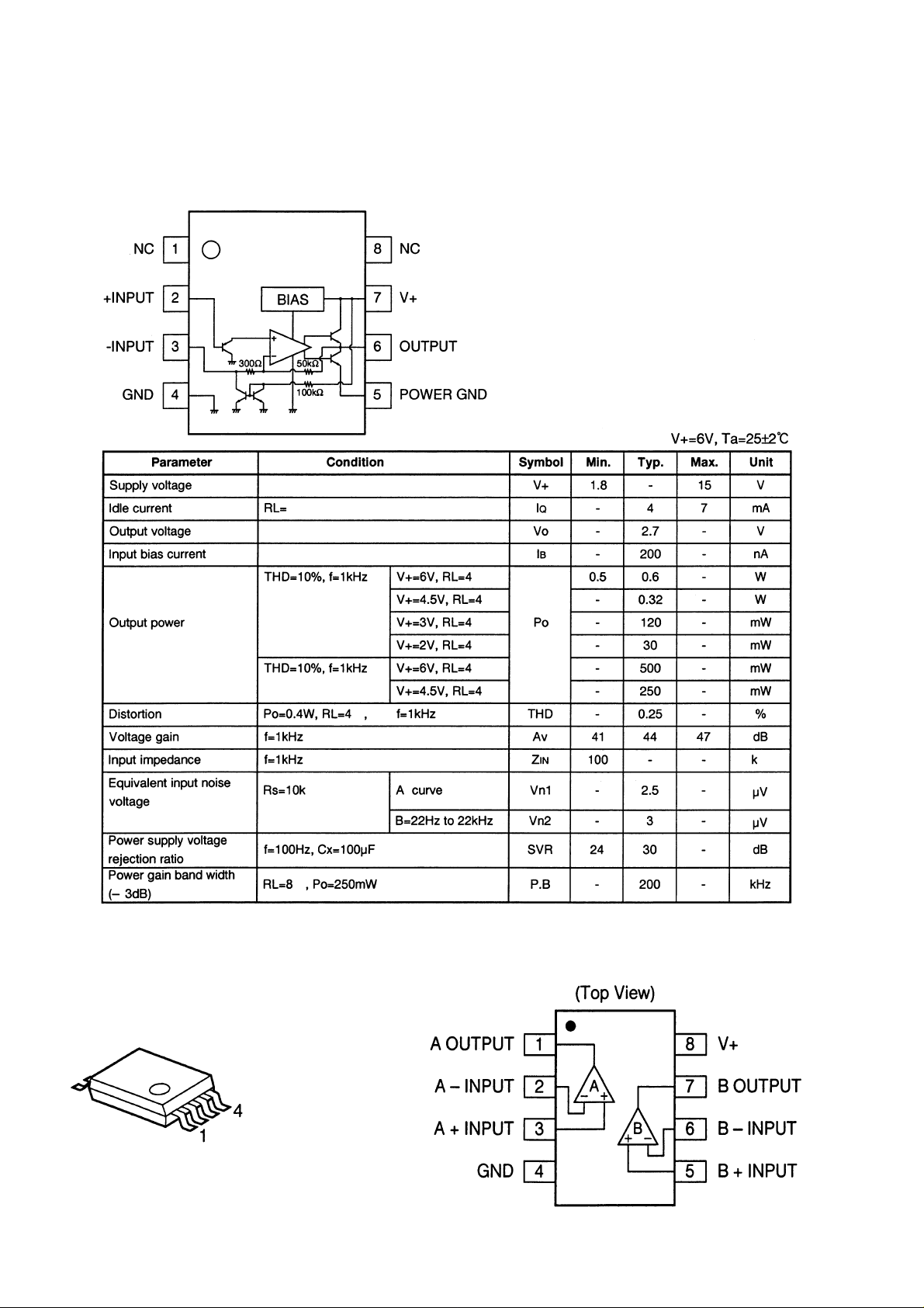
2) NJM2070MT1 (XA210)
Low V oltage P ower Amplifier
Equivalent Circuit
3) NJM2904V-TE1 (XA0573)
8
Page 9
4) NJM2902V-TE1 (XA0596)
Quad Single Supply Operational Amplifier
5) TA31136FN (XA0404)
Low Power FM IF
9
Page 10

6) UPC2771T(XA0545)
Terminal Connection
(Top View)
3
2
1
C2H
7) CAT24WC16JITE13 (XA0855)
PDIP
A0
A1
A2
Vss SDA
Vcc
WP
SCL
8) S-816A30AMC (XA0848)
4
1: INPUT
2: GND
3: GND
5
4: OUTPUT
5: GND
6
6: Vcc
Name
A0..A2
Vss
SDA
SCL
WP Write Protect Input
Vcc
User Configurable Chip Selects
Ground
Serial Address/Data I/O
Serial Clock
2.5V~6.0V Power Supply
Function
SOT-23-5
Top view
54
MC
1
23
IN
ON/OFF
V
EXT
IN
41
S-816A
3
2
OUT
V
OUT
~
R = 0.3Ω
5
CL
V
SS
10
Page 11

9) S-80827ALNP (XA0857)
Pin Assignment
Block Diagram
V
DD
Top view
34
1 OUT
2 V
3 NC
4 V
12
DD
SS
OUT
V
V
CC
10) MRF9745T1 (XE0034)
PAKEGE DIMENSIONS
REF
1
34
STYLE 1 :
PIN 1. DRAIN
2. GATE
3. SOURCE
2
4. SOURCE
11
Page 12

11) Transistor, Diode and LED Outline Drawings
1SV307(TPH3)
XD0326
TX
2SC5066-O(TE85L)
XT0138
MA2S728-TX
XD0315
B
XP1114 (TX)
XU0161
2SA1036K T146Q
XT110
2SD2216R-TX
XT0135
MA741WA TX
XD0251
XP1501-TX
XU0172
2SA1576A
XT0094
C
FR
BE
2SK3074
XE0044
WA
GDS
MA729-TX
XD0291
UMC5N TR
XU0152
2SB766A-TX
XT0170
DA204U
XD0130
K
MRF9745T1
XE0034
2SC4081 T106R
XT0095
HSU277TRF
XD331
RN1107 TE85L
XU0193
2SC4618TLP
XT0172
ISV311(TPL3)
XD0344
V1
RN2107 TE85L
XU0192
2SC4808-TX. AR
XT0171
M1FE 40400V1A
XD0368
SML-310MTT86
XL0036
12
Page 13

12) LCD connection
Pin No COM0 COM1 COM2 COM3
1 COM0 - - 2 - COM1 - 3 - - COM2 4 - - - COM3
5DEFC
6HI JG
7LMNK
8POVW
9RSUT
10 9c 9b 9a Y
11 9e 9g 9f 9d
12 8c 8b 8a X
13 8e 8g 8f 8d
14 7c 7b 7a Z
15 7e 7g 7f 7d
16 6c 6b 6a 6h
17 6e 6g 6f 6d
18 5c 5b 5a Q
19 5e 5g 5f 5d
20 4c 4b 4a 4h
21 4e 4g 4f 4d
22 3c 3b 3a B2
23 3e 3g 3f 3d
24 2c 2b 2a B1
25 2e 2g 2f 2d
26 1c 1b 1a A
27 1e 1g 1f 1d
13
Page 14
EXPLODED VIEW
1) Front View
TN0014
TZ0088
UR0023
UP0433
TL0027
DG0040
TL0026
EL0053
FG0330
14
ST0069
KZ0134
YX0032
DP0139
Page 15
2) Bottom View
AF0025
AF0031
FG0336
FG0345
RD0108
FM0201
FG0329
UP0433
SD0092
TS0165
FG0346
SD0093
FG0331
RED(MRCL04AA
BLUE(MACL04AA
ES0025
FP0182
)
)
FG0333
AN0012
AN0027
NK0077
SP0013
UE0338
FG0337
FG0332
AX0008
FG0334
AX0005
15
Page 16
PARTS LIST
MAIN Unit
Ref.
Parts No. Description Parts Name
No. T E TA
UP0433 PC Board DJS40 INTEGRATED 0.5 0.5 0.5
C1 CU3531 Chip C. GRM36B471K50PT 1 1 1
C2 CU3547 Chip C. GRM36B103K16PT 1 1 1
C3 CU3531 Chip C. GRM36B471K50PT 1 1 1
C4 CU3531 Chip C. GRM36B471K50PT 1 1 1
C5 CU3547 Chip C. GRM36B103K16PT 1 1 1
C6 CU3535 Chip C. GRM36B102K50PT 1 1 1
C7 CS0408 Chip tantalum 6MCM156MATER 1 1 1
C8 CU3511 Chip C. GRM36CH100D50PT 1 1 1
C10 CU3531 Chip C. GRM36B471K50PT 1 1 1
C11 CU3008 Chip C. C1608CH1H070CT-A 1 1 1
C12 CU3531 Chip C. GRM36B471K50PT 1 1 1
C14 CS0411 Chip tantalum 4MCM226MATER 1 1 1
C15 CU3531 Chip C. GRM36B471K50PT 1 1 1
C16 CU3531 Chip C. GRM36B471K50PT 1 1 1
C17 CU3531 Chip C. GRM36B471K50PT 1 1 1
C18 CU3531 Chip C. GRM36B471K50PT 1 1 1
C19 CU3531 Chip C. GRM36B471K50PT 1 1 1
C20 CU3531 Chip C. GRM36B471K50PT 1 1 1
C21 CU3008 Chip C. C1608CH1H070CT-A 1 1 1
C22 CU3531 Chip C. GRM36B471K50PT 1 1 1
C23 CU3507 Chip C. GRM36CH060D50PT 1 1 1
C24 CU3531 Chip C. GRM36B471K50PT 1 1 1
C25 CU3531 Chip C. GRM36B471K50PT 1 1 1
C26 CU3505 Chip C. GRM36CH040C50PT 1 1 1
C27 CU3510 Chip C. GRM36CH090D50PT 1 1 1
C28 CU3508 Chip C. GRM36CH070D50PT 1 1 1
C29 CU3511 Chip C. GRM36CH100D50PT 1 1 1
C30 CU3111 Chip C. C1608JB1C104KT-N 1 1 1
C32 CU3502 Chip C. GRM36CK010C50PT 1 1 1
C34 CU3501 Chip C. GRM36CK0R5C50PT 1 1 1
C35 CU3503 Chip C. GRM36CK020C50PT 1 1 1
C36 CU3515 Chip C. GRM36CH220J50PT 1 1 1
C37 CU3514 Chip C. GRM36CH180J50PT 1 1 1
C38 CU3509 Chip C. GRM36CH080D50PT 1 1 1
C39 CU3111 Chip C. C1608JB1C104KT-N 1 1 1
C40 CU3502 Chip C. GRM36CK010C50PT 1 1 1
C41 CU3503 Chip C. GRM36CK020C50PT 1 1 1
C42 CU3503 Chip C. GRM36CK020C50PT 1 1 1
C44 CU3501 Chip C. GRM36CK0R5C50PT 1 1 1
C46 CU3101 Chip C. C1608JB1C473KT-NS 1 1 1
C47 CS0406 Chip tantalum 35MCM105MATER 1 1 1
C48 CU3505 Chip C. GRM36CH040C50PT 1 1 1
C50 CU3111 Chip C. C1608JB1C104KT-N 1 1 1
C51 CU3531 Chip C. GRM36B471K50PT 1 1 1
C52 CU3531 Chip C. GRM36B471K50PT 1 1 1
C53 CU0108 Chip C. LMK212BJ105KG 1 1 1
C54 CU3531 Chip C. GRM36B471K50PT 1 1 1
C55 CU3523 Chip C. GRM36CH101J50PT 1 1 1
C56 CU3520 Chip C. GRM36CH560J50PT 1 1 1
C57 CU3516 Chip C. GRM36CH270J50PT 1 1 1
C58 CU3511 Chip C. GRM36CH100D50PT 1 1 1
C59 CU3535 Chip C. GRM36B102K50PT 1 1 1
C60 CU3531 Chip C. GRM36B471K50PT 1 1 1
C61 CU3535 Chip C. GRM36B102K50PT 1 1 1
C62 CU3547 Chip C. GRM36B103K16PT 1 1 1
C63 CU3547 Chip C. GRM36B103K16PT 1 1 1
C64 CU3111 Chip C. C1608JB1C104KT-N 1 1 1
Version
Ref.
Parts No. Description Parts Name
No. T E TA
C65 CS0367 Chip tantalum TMCMA0J106MTR 1 1 1
C66 CU3531 Chip C. GRM36B471K50PT 1 1 1
C67 CU3531 Chip C. GRM36B471K50PT 1 1 1
C68 CU3547 Chip C. GRM36B103K16PT 1 1 1
C69 CU3527 Chip C. GRM36CH221J25PT 1 1 1
C70 CU3505 Chip C. GRM36CH040C50PT 0 1 0
C70 CU3504 Chip C. GRM36CJ030C50PT 1 0 1
C71 CU3504 Chip C. GRM36CJ030C50PT 1 1 1
C72 CU3504 Chip C. GRM36CJ030C50PT 1 1 1
C73 CU3503 Chip C. GRM36CK020C50PT 1 1 1
C74 CU3502 Chip C. GRM36CK010C50PT 1 1 1
C75 CU3503 Chip C. GRM36CK020C50PT 1 1 1
C76 CU3503 Chip C. GRM36CK020C50PT 1 1 1
C77 CU3502 Chip C. GRM36CK010C50PT 1 1 1
C79 CU3510 Chip C. GRM36CH090D50PT 1 1 1
C80 CU3503 Chip C. GRM36CK020C50PT 1 1 1
C81 CU3508 Chip C. GRM36CH070D50PT 1 1 1
C82 CU3527 Chip C. GRM36CH221J25PT 1 1 1
C83 CU3531 Chip C. GRM36B471K50PT 1 1 1
C84 CU3503 Chip C. GRM36CK020C50PT 1 1 1
C85 CU3515 Chip C. GRM36CH220J50PT 1 1 1
C86 CU3503 Chip C. GRM36CK020C50PT 1 1 1
C87 CU3510 Chip C. GRM36CH090D50PT 1 1 1
C90 CU3507 Chip C. GRM36CH060D50PT 1 1 1
C92 CU3502 Chip C. GRM36CK010C50PT 1 1 1
C93 CU3523 Chip C. GRM36CH101J50PT 1 1 1
C95 CU3111 Chip C. C1608JB1C104KT-N 1 1 1
C96 CU3522 Chip C. GRM36CH820J50PT 1 1 1
C97 CU3535 Chip C. GRM36B102K50PT 1 1 1
C98 CU3535 Chip C. GRM36B102K50PT 1 1 1
C100 CU3535 Chip C. GRM36B102K50PT 1 1 1
C101 CU3551 Chip C. GRM36B223K16PT 1 1 1
C102 CU3539 Chip C. GRM36B222K50PT 1 1 1
C103 CU3539 Chip C. GRM36B222K50PT 1 1 1
C104 CU3547 Chip C. GRM36B103K16PT 1 1 1
C105 CU0108 Chip C. LMK212BJ105KG 1 1 1
C106 CU3551 Chip C. GRM36B223K16PT 1 1 1
C107 CU3101 Chip C. C1608JB1C473KT-NS 1 1 1
C108 CU3524 Chip C. GRM36CH121J50PT 1 1 1
C109 CU3111 Chip C. C1608JB1C104KT-N 1 1 1
C110 CU3111 Chip C. C1608JB1C104KT-N 1 1 1
C111 CU3111 Chip C. C1608JB1C104KT-N 1 1 1
C112 CU3111 Chip C. C1608JB1C104KT-N 1 1 1
C113 CU3547 Chip C. GRM36B103K16PT 1 1 1
C114 CU3111 Chip C. C1608JB1C104KT-N 1 1 1
C115 CU3111 Chip C. C1608JB1C104KT-N 1 1 1
C116 CU3541 Chip C. GRM36B332K50PT 1 1 1
C117 CU3535 Chip C. GRM36B102K50PT 1 1 1
C118 CS0408 Chip tantalum 6MCM156MATER 1 1 1
C119 CU0108 Chip C. LMK212BJ105KG 1 1 1
C120 CU3538 Chip C. GRM36B182K50PT 1 1 1
C121 CU3101 Chip C. C1608JB1C473KT-NS 1 1 1
C122 CU3523 Chip C. GRM36CH101J50PT 1 1 1
C123 CU3547 Chip C. GRM36B103K16PT 1 1 1
C124 CU3111 Chip C. C1608JB1C104KT-N 1 1 1
C125 CU3549 Chip C. GRM36B153K16PT 1 1 1
C126 CU0108 Chip C. LMK212BJ105KG 1 1 1
C127 CU3547 Chip C. GRM36B103K16PT 1 1 1
Version
16
Page 17

Ref.
Parts No. Description Parts Name
No. T E TA
C128 CU3551 Chip C. GRM36B223K16PT 1 1 1
C129 CS0367 Chip tantalum TMCMA0J106MTR 1 1 1
C130 CS0414 Chip tantalum 6MCM476MB2TER 1 1 1
C131 CS0408 Chip tantalum 6MCM156MATER 1 1 1
C132 CU3544 Chip C. GRM36B562K25PT 1 1 1
C133 CU3540 Chip C. GRM36B272K50PT 1 1 1
C134 CU3547 Chip C. GRM36B103K16PT 1 1 1
C135 CU3545 Chip C. GRM36B682K25PT 1 1 1
C137 CU3543 Chip C. GRM36B472K25PT 1 1 1
C138 CU3111 Chip C. C1608JB1C104KT-N 1 1 1
C139 CU3535 Chip C. GRM36B102K50PT 1 1 1
C140 CU0108 Chip C. LMK212BJ105KG 1 1 1
C141 CU3111 Chip C. C1608JB1C104KT-N 1 1 1
C142 CU3535 Chip C. GRM36B102K50PT 1 1 1
C143 CU3547 Chip C. GRM36B103K16PT 1 1 1
C144 CS0408 Chip tantalum 6MCM156MATER 1 1 1
C145 CU3535 Chip C. GRM36B102K50PT 1 1 1
C146 CS0408 Chip tantalum 6MCM156MATER 1 1 1
C147 CS0422 Chip tantalum TMCMB1A476MTR 1 1 1
C148 CU0108 Chip C. LMK212BJ105KG 1 1 1
C149 CU3111 Chip C. C1608JB1C104KT-N 1 1 1
C150 CU3551 Chip C. GRM36B223K16PT 1 1 1
C151 CU3551 Chip C. GRM36B223K16PT 1 1 1
C152 CU3111 Chip C. C1608JB1C104KT-N 1 1 1
C157 CE0411 Electrolytic C. 16MV10UWA3 1 1 1
C158 CS0414 Chip tantalum 6MCM476MB2TER 1 1 1
C159 CU3535 Chip C. GRM36B102K50PT 1 1 1
C160 CU0108 Chip C. LMK212BJ105KG 1 1 1
C161 CU3535 Chip C. GRM36B102K50PT 1 1 1
C162 CU3517 Chip C. GRM36CH330J50PT 1 1 1
C163 CU3517 Chip C. GRM36CH330J50PT 1 1 1
C165 CU3535 Chip C. GRM36B102K50PT 1 1 1
C166 CS0414 Chip tantalum 6MCM476MB2TER 1 1 1
C167 CU3503 Chip C. GRM36CK020C50PT 1 1 1
C168 CU3531 Chip C. GRM36B471K50PT 1 1 1
C169 CU3531 Chip C. GRM36B471K50PT 1 1 1
C170 CU3111 Chip C. C1608JB1C104KT-N 1 1 1
C171 CU3535 Chip C. GRM36B102K50PT 1 1 1
C172 CU3535 Chip C. GRM36B102K50PT 1 1 1
C173 CE0411 Electrolytic C. 16MV10UWA3 1 1 1
C174 CS0367 Chip tantalum TMCMA0J106MTR 1 1 1
C175 CU3111 Chip C. C1608JB1C104KT-N 1 1 1
C178 CU3519 Chip C. GRM36CH470J50PT 1 1 1
C179 CU3519 Chip C. GRM36CH470J50PT 1 1 1
C180 CU3535 Chip C. GRM36B102K50PT 1 1 1
C181 CU3535 Chip C. GRM36B102K50PT 1 1 1
C182 CU3519 Chip C. GRM36CH470J50PT 1 1 1
C184 CU3510 Chip C. GRM36CH090D50PT 1 0 1
C184 CU3511 Chip C. GRM36CH100D50PT 0 1 0
C185 CU3503 Chip C. GRM36CK020C50PT 1 1 1
C186 CU3111 Chip C. C1608JB1C104KT-N 1 1 1
C187 CU3111 Chip C. C1608JB1C104KT-N 1 1 1
C188 CU3509 Chip C. GRM36CH080D50PT 1 1 1
C209 CU3535 Chip C. GRM36B102K50PT 1 1 1
C210 CU3531 Chip C. GRM36B471K50PT 1 1 1
C212 CU0108 Chip C. LMK212BJ105KG 1 1 1
C213 CU3004 Chip C. C1608CH1H030CT-AS 1 1 1
D1 XD0326 Chip Diode 1SV307(TPH3) 1 1 1
D2 XD0344 Chip Diode 1SV311 (TPL3) 1 1 1
D3 XD0331 Chip Diode HSU277TRF 1 1 1
D4 XD0251 Chip Diode MA741WA TX 1 1 1
D5 XD0331 Chip Diode HSU277TRF 1 1 1
D6 XD0291 Chip Diode MA729-TX 1 1 1
D7 XD0368 Chip Diode M1FE40-4063 1 1 1
Version
Ref.
Parts No. Description Parts Name
No. T E TA
D8 XL0036 Chip Diode SML-310MTT86 1 1 1
D10 XL0036 Chip Diode SML-310MTT86 1 1 1
D11 XD0331 Chip Diode HSU277TRF 1 1 1
D13 XD0130 Chip Diode DA204U T106 1 1 1
D15 XD0344 Chip Diode 1SV311 (TPL3) 1 1 1
D16 XD0291 Chip Diode MA729-TX 1 1 1
D17 XD0315 Chip Diode MA2S728-TX 1 1 1
EL1 EL0053 LCD WD-S2304I-7TNNAA 1 1 1
FL2 XC0075 Ceramic Filter CFUCG450E-TC 1 1 1
FL3 XF0034 Crystal Filter DSF753S 21.700MHZ 1 1 1
IC1 XA0545 IC UPC2771T 1 1 1
IC2 XA0543 IC M64082AGP 1 1 1
IC3 XA0404 IC TA31136FN(EL) 1 1 1
IC4 XA0573 IC NJM2904V-TE1 1 1 1
IC5 XA0596 IC NJM2902V-TE1 1 1 1
IC6 XA0210 IC NJM2070M T1 1 1 1
IC7 XA0903 IC M38224M6M233HP DJS40 1 1 1
IC9 XA0817 IC S-24C16AFJX-TB-01 1 1 1
IC10 XA0848 IC S-816A30AMC-BAF-T2 1 1 1
IC11 XA0857 IC S-80827ALNP 1 1 1
JK1 UJ0022 Jack HSJ1102-01-540 1 1 1
JK2 UJ0019 Jack HSJ1493-01-010 1 1 1
JK3 UJ0015 Jack HEC2781 010020 1 1 1
L1 QC0215 Chip Inductor MLF2012A1R0K-T 1 1 1
L2 QC0533 Chip Inductor LQN21A39NJ04 1 1 1
L3 QC0507 Chip Inductor LK16081R0K-T 1 1 1
L4 QC0623 Chip Inductor LL1608-FS47NJ 1 1 1
L5 QC0627 Chip Inductor LL1608-FSR10J 1 1 1
L6 QKA45A Coil MR1.5 4.5T 0.4 1 1 1
L7 QKA45A Coil MR1.5 4.5T 0.4 1 1 1
L8 QKA25A Coil MR1.5 2.5T 0.4 1 1 1
L9 QC0619 Chip Inductor LL1608-FS22NJ 1 1 1
L10 QC0616 Chip Inductor LL1608-FS12NJ 1 1 1
L11 QC0616 Chip Inductor LL1608-FS12NJ 1 1 1
L12 QC0527 Chip Inductor LQN21A12NJ04 1 1 1
L13 QC0507 Chip Inductor LK16081R0K-T 1 1 1
L14 QC0527 Chip Inductor LQN21A12NJ04 1 1 1
L15 QC0528 Chip Inductor LQN21A15NJ04 1 1 1
L16 QC0507 Chip Inductor LK16081R0K-T 1 1 1
L17 QC0618 Chip Inductor LL1608-FS18NJ 1 1 1
L18 QC0526 Chip Inductor LQN21A10NJ04 1 1 1
L19 QC0526 Chip Inductor LQN21A10NJ04 1 1 1
L20 QC0527 Chip Inductor LQN21A12NJ04 1 1 1
L21 QC0527 Chip Inductor LQN21A12NJ04 1 1 1
L22 QC0507 Chip Inductor LK16081R0K-T 1 1 1
L23 QC0623 Chip Inductor LL1608-FS47NJ 1 1 1
L24 QC0534 Chip Inductor LQN21A47NJ04 1 1 1
L25 QC0616 Chip Inductor LL1608-FS12NJ 1 1 1
MIC1 EY0017 Mic OB-27P44 1 1 1
Q1 XU0193 Chip Transistor RN1107 TE85L 1 1 1
Q2 XT0138 Chip Transistor 2SC5066-O(TE85L) 1 1 1
Q3 XE0034 FET MRF9745T1 1 1 1
Q4 XE0044 FET 2SK3074 TE12L 1 1 1
Q5 XU0172 Chip Transistor XP1501-TX 1 1 1
Q6 XT0138 Chip Transistor 2SC5066-O(TE85L) 1 1 1
Q7 XT0138 Chip Transistor 2SC5066-O(TE85L) 1 1 1
Q8 XT0172 Chip Transistor 2SC4618TLP 1 1 1
Q9 XT0138 Chip Transistor 2SC5066-O(TE85L) 1 1 1
Q10 XT0138 Chip Transistor 2SC5066-O(TE85L) 1 1 1
Q11 XT0138 Chip Transistor 2SC5066-O(TE85L) 1 1 1
Q12 XT0171 Chip Transistor 2SC4808-TX.AR 1 1 1
Q13 XU0092 Chip Transistor UN911H-TX 1 1 1
Q15 XT0095 Chip Transistor 2SC4081 T106R 1 1 1
Q16 XU0193 Chip Transistor RN1107 TE85L 1 1 1
Version
17
Page 18

Ref.
Parts No. Description Parts Name
No. T E TA
Q17 XT0170 Chip Transistor 2SB766A-TX 1 1 1
Q19 XT0095 Chip Transistor 2SC4081 T106R 1 1 1
Q20 XT0135 Chip Transistor 2SD2216R-TX 1 1 1
Q21 XT0110 Chip Transistor 2SA1036K T146Q 1 1 1
Q22 XU0161 Chip Transistor XP1114(TX) 1 1 1
Q23 XT0135 Chip Transistor 2SD2216R-TX 1 1 1
Q24 XU0193 Chip Transistor RN1107 TE85L 1 1 1
Q26 XU0172 Chip Transistor XP1501-TX 1 1 1
Q27 XT0170 Chip Transistor 2SB766A-TX 1 1 1
Q28 XU0152 Chip Transistor UMC5NTR 1 1 1
Q29 XU0192 Chip Transistor RN2107 TE85L 1 1 1
Q30 XU0172 Chip Transistor XP1501-TX 1 1 1
Q31 XT0094 Chip Transistor 2SA1576A T106R 1 1 1
Q32 XT0170 Chip Transistor 2SB766A-TX 1 1 1
Q35 XU0192 Chip Transistor RN2107 TE85L 1 1 1
Q36 XU0193 Chip Transistor RN1107 TE85L 1 1 1
Q39 XT0110 Chip Transistor 2SA1036K T146Q 1 1 1
Q40 XT0135 Chip Transistor 2SD2216R-TX 1 1 1
R4 RK3550 Chip R. ERJ2GEJ103X 1 1 1
R5 RK3526 Chip R. ERJ2GEJ101X 1 1 1
R6 RK3558 Chip R. ERJ2GEJ473X 1 1 1
R8 RK3558 Chip R. ERJ2GEJ473X 1 1 1
R9 RK3522 Chip R. ERJ2GEJ470X 1 1 1
R11 RK3522 Chip R. ERJ2GEJ470X 1 1 1
R12 RK3572 Chip R. ERJ2GEJ684X 1 1 1
R13 RK3562 Chip R. ERJ2GEJ104X 1 1 1
R14 RK3562 Chip R. ERJ2GEJ104X 1 1 1
R15 RK3522 Chip R. ERJ2GEJ470X 1 1 1
R16 RK3526 Chip R. ERJ2GEJ101X 1 1 1
R17 RK3546 Chip R. ERJ2GEJ472X 1 1 1
R18 RK3522 Chip R. ERJ2GEJ470X 1 1 1
R19 RK3546 Chip R. ERJ2GEJ472X 1 1 1
R20 RK3550 Chip R. ERJ2GEJ103X 1 1 1
R21 RK3545 Chip R. ERJ2GEJ392X 1 1 1
R22 RK3558 Chip R. ERJ2GEJ473X 1 1 1
R23 RK3550 Chip R. ERJ2GEJ103X 1 1 1
R24 RK3544 Chip R. ERJ2GEJ332X 1 1 1
R25 RK3566 Chip R. ERJ2GEJ224X 1 1 1
R26 RK3562 Chip R. ERJ2GEJ104X 1 1 1
R28 RK3534 Chip R. ERJ2GEJ471X 1 1 1
R29 RK3530 Chip R. ERJ2GEJ221X 1 1 1
R31 RK3544 Chip R. ERJ2GEJ332X 1 1 1
R32 RK3556 Chip R. ERJ2GEJ333X 1 1 1
R33 RK3530 Chip R. ERJ2GEJ221X 1 1 1
R34 RK3544 Chip R. ERJ2GEJ332X 1 1 1
R35 RK3518 Chip R. ERJ2GEJ220X 1 1 1
R36 RK3554 Chip R. ERJ2GEJ223X 1 1 1
R37 RK3518 Chip R. ERJ2GEJ220X 1 1 1
R38 RK3538 Chip R. ERJ2GEJ102X 1 1 1
R39 RK3538 Chip R. ERJ2GEJ102X 1 1 1
R40 RK3526 Chip R. ERJ2GEJ101X 1 1 1
R41 RK3526 Chip R. ERJ2GEJ101X 1 1 1
R42 RK3526 Chip R. ERJ2GEJ101X 1 1 1
R43 RK3518 Chip R. ERJ2GEJ220X 1 1 1
R44 RK3538 Chip R. ERJ2GEJ102X 1 1 1
R45 RK3544 Chip R. ERJ2GEJ332X 1 1 1
R46 RK3530 Chip R. ERJ2GEJ221X 1 1 1
R47 RK3530 Chip R. ERJ2GEJ221X 1 1 1
R48 RK3566 Chip R. ERJ2GEJ224X 1 1 1
R49 RK3559 Chip R. ERJ2GEJ563X 1 1 1
R50 RK3559 Chip R. ERJ2GEJ563X 1 1 1
R51 RK3562 Chip R. ERJ2GEJ104X 1 1 1
R52 RK3539 Chip R. ERJ2GEJ122X 1 1 1
R53 RK3539 Chip R. ERJ2GEJ122X 1 1 1
Version
Ref.
Parts No. Description Parts Name
No. T E TA
R54 RK3550 Chip R. ERJ2GEJ103X 1 1 1
R55 RK3564 Chip R. ERJ2GEJ154X 1 1 1
R56 RK3526 Chip R. ERJ2GEJ101X 1 1 1
R59 RK3540 Chip R. ERJ2GEJ152X 1 1 1
R61 RK3562 Chip R. ERJ2GEJ104X 1 1 1
R62 RK1018 Chip R. ERJ8GEYJ101V 1 1 1
R63 RK3554 Chip R. ERJ2GEJ223X 1 1 1
R64 RK3558 Chip R. ERJ2GEJ473X 1 1 1
R66 RK3562 Chip R. ERJ2GEJ104X 1 1 1
R67 RK3501 Chip R. ERJ2GE0R00X 1 1 1
R68 RK3552 Chip R. ERJ2GEJ153X 1 1 1
R69 RK3548 Chip R. ERJ2GEJ682X 1 1 1
R70 RK3555 Chip R. ERJ2GEJ273X 1 1 1
R71 RK3562 Chip R. ERJ2GEJ104X 1 1 1
R72 RK3562 Chip R. ERJ2GEJ104X 1 1 1
R73 RK3556 Chip R. ERJ2GEJ333X 1 1 1
R75 RK3562 Chip R. ERJ2GEJ104X 1 1 1
R76 RK3550 Chip R. ERJ2GEJ103X 1 1 1
R77 RK3572 Chip R. ERJ2GEJ684X 1 1 1
R78 RK3562 Chip R. ERJ2GEJ104X 1 1 1
R79 RK3558 Chip R. ERJ2GEJ473X 1 1 1
R80 RK3558 Chip R. ERJ2GEJ473X 1 1 1
R81 RK3550 Chip R. ERJ2GEJ103X 1 1 1
R82 RK3522 Chip R. ERJ2GEJ470X 1 1 1
R83 RK3557 Chip R. ERJ2GEJ393X 1 1 1
R84 RK3554 Chip R. ERJ2GEJ223X 1 1 1
R85 RK3558 Chip R. ERJ2GEJ473X 1 1 1
R86 RK3548 Chip R. ERJ2GEJ682X 1 1 1
R87 RK3559 Chip R. ERJ2GEJ563X 1 1 1
R88 RK3558 Chip R. ERJ2GEJ473X 1 1 1
R89 RK3538 Chip R. ERJ2GEJ102X 1 1 1
R90 RK3567 Chip R. ERJ2GEJ274X 1 1 1
R91 RK3545 Chip R. ERJ2GEJ392X 1 1 1
R92 RK3563 Chip R. ERJ2GEJ124X 1 1 1
R93 RK3558 Chip R. ERJ2GEJ473X 1 1 1
R94 RK3561 Chip R. ERJ2GEJ823X 1 1 1
R95 RK3550 Chip R. ERJ2GEJ103X 1 1 1
R96 RK3543 Chip R. ERJ2GEJ272X 1 1 1
R97 RK3542 Chip R. ERJ2GEJ222X 1 1 1
R98 RK3545 Chip R. ERJ2GEJ392X 1 1 1
R99 RK3560 Chip R. ERJ2GEJ683X 1 1 1
R100 RK3550 Chip R. ERJ2GEJ103X 1 1 1
R101 RK3563 Chip R. ERJ2GEJ124X 1 1 1
R102 RK3552 Chip R. ERJ2GEJ153X 1 1 1
R103 RK3559 Chip R. ERJ2GEJ563X 1 1 1
R104 RK3563 Chip R. ERJ2GEJ124X 1 1 1
R105 RK3546 Chip R. ERJ2GEJ472X 1 1 1
R106 RK3540 Chip R. ERJ2GEJ152X 1 1 1
R107 RK3514 Chip R. ERJ2GEJ100X 1 1 1
R108 RK3550 Chip R. ERJ2GEJ103X 1 1 1
R109 RK3550 Chip R. ERJ2GEJ103X 1 1 1
R111 RK3550 Chip R. ERJ2GEJ103X 1 1 1
R112 RK3572 Chip R. ERJ2GEJ684X 1 1 1
R113 RK3550 Chip R. ERJ2GEJ103X 1 1 1
R114 RK3567 Chip R. ERJ2GEJ274X 1 1 1
R115 RK3560 Chip R. ERJ2GEJ683X 1 1 1
R116 RK3538 Chip R. ERJ2GEJ102X 1 1 1
R117 RK3546 Chip R. ERJ2GEJ472X 1 1 1
R118 RK3526 Chip R. ERJ2GEJ101X 1 1 1
R119 RK3538 Chip R. ERJ2GEJ102X 1 1 1
R120 RK3546 Chip R. ERJ2GEJ472X 1 1 1
R121 RK3550 Chip R. ERJ2GEJ103X 1 1 1
R122 RK3546 Chip R. ERJ2GEJ472X 1 1 1
R123 RK3546 Chip R. ERJ2GEJ472X 1 1 1
Version
18
Page 19

Ref.
Parts No. Description Parts Name
No. T E TA
R124 RK3550 Chip R. ERJ2GEJ103X 1 1 1
R125 RK3562 Chip R. ERJ2GEJ104X 1 1 1
R126 RK3546 Chip R. ERJ2GEJ472X 1 1 1
R127 RK3550 Chip R. ERJ2GEJ103X 1 1 1
R128 RK3542 Chip R. ERJ2GEJ222X 1 1 1
R129 RK3541 Chip R. ERJ2GEJ182X 1 1 1
R130 RK3564 Chip R. ERJ2GEJ154X 1 1 1
R131 RK3550 Chip R. ERJ2GEJ103X 1 1 1
R132 RK3566 Chip R. ERJ2GEJ224X 1 1 1
R133 RK3542 Chip R. ERJ2GEJ222X 1 1 1
R134 RK3542 Chip R. ERJ2GEJ222X 1 1 1
R135 RK3551 Chip R. ERJ2GEJ123X 1 1 1
R136 RK3522 Chip R. ERJ2GEJ470X 1 1 1
R137 RK3532 Chip R. ERJ2GEJ331X 1 1 1
R138 RK3562 Chip R. ERJ2GEJ104X 1 1 1
R139 RK3558 Chip R. ERJ2GEJ473X 1 1 1
R140 RK3558 Chip R. ERJ2GEJ473X 1 1 1
R141 RK3562 Chip R. ERJ2GEJ104X 1 1 1
R142 RK3558 Chip R. ERJ2GEJ473X 1 1 1
R143 RK3562 Chip R. ERJ2GEJ104X 1 1 1
R144 RK3574 Chip R. ERJ2GEJ105X 1 1 1
R145 RK3562 Chip R. ERJ2GEJ104X 1 1 1
R146 RK3529 Chip R. ERJ2GEJ181X 1 1 1
R147 RK3552 Chip R. ERJ2GEJ153X 1 1 1
R148 RK3562 Chip R. ERJ2GEJ104X 1 1 1
R149 RK3562 Chip R. ERJ2GEJ104X 1 1 1
R150 RK3562 Chip R. ERJ2GEJ104X 1 1 1
R151 RK3574 Chip R. ERJ2GEJ105X 1 1 1
R153 RK3538 Chip R. ERJ2GEJ102X 1 0 1
R156 RK3546 Chip R. ERJ2GEJ472X 1 1 1
R157 RK3546 Chip R. ERJ2GEJ472X 1 1 1
R159 RK3542 Chip R. ERJ2GEJ222X 1 1 1
R160 RK3538 Chip R. ERJ2GEJ102X 1 1 1
R161 RK3538 Chip R. ERJ2GEJ102X 1 1 1
R162 RK3551 Chip R. ERJ2GEJ123X 1 1 1
R163 RK3562 Chip R. ERJ2GEJ104X 1 1 1
R164 RK3558 Chip R. ERJ2GEJ473X 1 1 1
R165 RK3550 Chip R. ERJ2GEJ103X 1 1 1
R167 RK3562 Chip R. ERJ2GEJ104X 1 1 1
R168 RK3538 Chip R. ERJ2GEJ102X 1 1 1
R169 RK0003 Chip R. ERJ6GEYJ150V 1 1 1
R170 RK3538 Chip R. ERJ2GEJ102X 1 1 1
R173 RK3501 Chip R. ERJ2GE0R00X 1 1 1
R174 RK3558 Chip R. ERJ2GEJ473X 1 1 1
R175 RK3550 Chip R. ERJ2GEJ103X 1 1 1
R176 RK3550 Chip R. ERJ2GEJ103X 1 1 1
R177 RK3538 Chip R. ERJ2GEJ102X 1 1 1
R178 RK3550 Chip R. ERJ2GEJ103X 1 1 1
R180 RK3550 Chip R. ERJ2GEJ103X 1 1 1
R182 RK3538 Chip R. ERJ2GEJ102X 1 1 1
R183 RK3538 Chip R. ERJ2GEJ102X 1 1 1
R190 RK3542 Chip R. ERJ2GEJ222X 1 1 1
R191 RK3550 Chip R. ERJ2GEJ103X 1 1 1
R192 RK3550 Chip R. ERJ2GEJ103X 1 1 1
R193 RK3552 Chip R. ERJ2GEJ153X 1 1 1
R194 RK3547 Chip R. ERJ2GEJ562X 1 1 1
R195 RK3501 Chip R. ERJ2GE0R00X 1 1 1
R196 RK3550 Chip R. ERJ2GEJ103X 1 1 1
R197 RK3562 Chip R. ERJ2GEJ104X 1 1 1
R198 RK3546 Chip R. ERJ2GEJ472X 1 1 1
R199 RK3529 Chip R. ERJ2GEJ181X 1 1 1
R200 RK3542 Chip R. ERJ2GEJ222X 1 1 1
R201 RK3574 Chip R. ERJ2GEJ105X 1 1 1
R202 RK3562 Chip R. ERJ2GEJ104X 0 0 0
Version
Ref.
Parts No. Description Parts Name
No. T E TA
R203 RK3558 Chip R. ERJ2GEJ473X 1 1 1
R204 RK3542 Chip R. ERJ2GEJ222X 1 1 1
R205 RK3562 Chip R. ERJ2GEJ104X 1 1 1
R206 RK3501 Chip R. ERJ2GE0R00X 1 1 1
R208 RK3548 Chip R. ERJ2GEJ682X 1 1 1
R209 RK3501 Chip R. ERJ2GE0R00X 1 1 1
R210 RK3501 Chip R. ERJ2GE0R00X 0 0 0
R211 RK3562 Chip R. ERJ2GEJ104X 1 1 1
R212 RK3554 Chip R. ERJ2GEJ223X 1 1 1
R213 RK3522 Chip R. ERJ2GEJ470X 1 1 1
R214 RK3538 Chip R. ERJ2GEJ102X 1 1 1
TC1 CT0046 Trimmer TC03C100A-TP02 1 1 1
TC2 CT0046 Trimmer TC03C100A-TP02 1 1 1
TC3 CT0046 Trimmer TC03C100A-TP02 1 1 1
VR1 RH0140 Trimmer R. MVR22HXBRN472 1 1 1
VR2 RH0140 Trimmer R. MVR22HXBRN472 1 1 1
VR3 RV0046 Volume TP76N00A135FB103 1 1 1
W6 MACLH2GG Wire #30AH1-025-H1 1 1 0
W7 UX1277 Wore WIRE DJS40 W7 1 1 1
X1 XQ0103 Crystal TOP-B 21.250MHZ 1 1 1
X2 XK0005 Discriminator CDBC450CX24-TC 1 1 1
X3 XQ0131 Crystal CSA310 3.686400MHZ 1 1 1
FM0196 RADIATE SHEET 1 1 1
DG0040 LCD LIGHT DJS40 1 1 1
ST0069 LCD HOLDER 1 1 1
TL0027 REFLECTION SHEET 1 1 1
TS0142 VCO case XH655 1 1 1
TS0148 VCO Shield DJP85 1 1 1
TL0026 DIFFUSION SHEET 1 1 1
Version
PTT Unit
Ref.
Parts No. Description Parts Name
No. T E TA
SW1 UU0027 Switch SKQGAA 1 1 1
SW7 UU0027 Switch SKQGAA 1 1 1
Version
19
Page 20

Mechanical Parts
Packing
Ref.
Parts No. Description Parts Name
No. T E TA
W1 MBCL02AA Wire #30B02-20-02 1 1 1
W2 MRCL02AA Wire #30R02-20-02 1 1 1
W3 MRCL02AA Wire #30R02-20-02 1 1 1
AF0025 Screw 0PH M2+2.5 FE/N1 2 2 2
AF0031 Screw 0PH 2+5 FE/N3 1 1 1
AN0012 Nut RND N7X0.75 BR/B.ZN 1 1 1
AN0027 Nut ANTENNA NUT XH720 1 1 1
AX0005 Screw OP 1.7+5.5 Fe NI3 2 2 2
AX0008 Screw OPH P1.7+4 FE/B.ZN3 2 2 2
DP0139 LCD panel 1 1 1
ES0025 Spesker 32-8BB-06 1 1 1
FG0329 PTT RUBBER 1 1 1
FG0330 SILICON KEY RUBBER 1 1 1
FG0331 TERMINAL RUBBER 2 2 2
FG0332 MIC CAP RUBBER 1 1 1
FG0333 JACK CAP RUBBER 1 1 1
FG0334 SP CAP RUBBER 1 1 1
FG0336 MIC RUBBER 1 1 1
FG0337 DC CAP RUBBER 1 1 1
FG0345 FLEXIBLE CUSHION S40 1 1 1
FG0346 CUSHION A DJS40 1 1 1
FM0201 ANTENNA GROUND DJS40 1 1 1
FP0179 REAR PANEL 1 1 1
FP0182 SP CUSHION 2 2 2
KZ0134A FRONT CASE ASSY DJS40 1 1 1
KZ0135A REAR CASE ASSY S40 1 1 1
W5 MACL04AA Wire #30A02-040-02 1 1 1
W4 MRCL04AA Wire #30 RED 02-040-02 1 1 1
NK0077 VOL KNOB DJS40 1 1 1
RD0108 J1/6Z 1 1 1
SD0092 TERMINAL L 1 1 1
SD0093 TERMINAL R 1 1 1
SP0013 LECTRA #7800 1 1 1
TN0014 FLEX. SHIELD 1 1 1
TN0014 FLEX. SHIELD 1 1 1
TS0165 RF SHIELD 1 1 1
TZ0088 INSULATOR DJS40J 1 1 1
UE0338 SMA 19-16-3TGG 1 1 1
YX0032 LCD TAPE DJS40 1 1 1
Version
Ref.
Parts No. Description Parts Name
No. T E TA
EBP-53N Ni-Cd Bttery Pack 1 1 0
EDC-93 AC Aadaptor(120V) 1 0 0
EDC-94 AC Aadaptor(230V) 0 1 0
EA0070AC Anntena 1 1 1
PH0013 Warranty 1 0 0
DS0446 Serial No. sheet 1 1 1
PK0087 Schematic 1 1 1
HK0520 Package 1 1 1
HM0215 Carton 1 1 1
HU0170 Carton Plate 1 1 1
HP0006Z Plastic Bag 1 1 1
PR0452 FCC Home use seal 1 0 0
PR0447 FCC Warnig 1 0 0
PS0405A Instruction 1 1 1
EDH-31 Battery Case 1 1 1
EBC-18 Belt Clip Strap 1 1 1
Version
20
Page 21

ADJUSTMENT
1. Enter the frequency in memory . (M1 ~ M17) * Refer to Memory Channel’s Frequency List
2. Press FUNC > MONI (Key Lock) > FUNC >
(It becomes in “Adjustment Mode” and “A” appears on the display)
3. Adjust the Set 1. (Refer to Adjustment Manual)
4. Press FUNC > MONI (Key Lock) > FUNC >
(It becomes in “Nomal Mode” and “A” disappears on the display)
Remark1.# The frequency in each Memory Channel can be changed within ±500KHz.
> 2 times > V/M > MONI 2 times
w
21
Page 22

Item Ch Frequency (MHz)
Status
Adj. or
Check
Terminal
Adj.
Point
Adj.Range Condition
1.
PD Voltage
2.
Reference
Frecuency
3.
High Power
output.
4.
High Power
current
5.
Low Power
output
6.
Sensitivity
1 E T
1 E T
2 E T
2 E T
3 E T
5 E T
TA
TA
TA
TA
TA
TA
:435.05
:435.05
:435.05
:435.05
:435.05
:435.05
:435.05
:445.05
:445.05
:435.05
:445.05
:445.05
:435.05
:445.05
:445.05
:435.05
:445.05
:445.05
Rx
and
Check TP2 --
Tx
Tx Adj. ANT TC1
Tx Adj. ANT VR1
Tx Check
Tx Check ANT --
Rx Adj.
DC
Jack
SP
Jack
--
TC2
and
TC3
Rx : 0.8 1.2V
Tx : 1.0 ∼∼1.4V
±100Hz
1.0 ±0.05W
less than
0.6A
∼
0.1 0.25W
less than
-7.0dB
The sensitivity must
be adjusted to the
best.
7.
S-meter (1)
8.
S-meter (5)
9.
Mic Deviation
10.
Tone
Deviation
16.
Tone burst
Deviation
17.
Aging test
7 E T
8 E T
9
13
16
17
TA
TA
E
T
TA
E
T
TA
E
T
TA
E
T
TA
:435.05
:445.05
:445.05
:435.05
:445.05
:445.05
:435.05
:445.05
:445.05
:435.05
:445.05
:445.05
:435.05
:445.05
:445.05
:435.50
:445.50
:445.50
Rx Adj. --
Rx Adj. --
Tx Adj. ANT VR2
Tx Check ANT --
Tx Check ANT --
Tx
and
Rx
FUNC
Key
FUNC
Key
-- RF sig. lev el : 0dBu
-- RF sig. lev el : 20dBu
AF sig. : 1KHz /
4.5 ±0.1KHz
∼
0.6 1.2KHz
∼
2.2 3.0KHz
50mVrms
AF Filter : OFF-20KHz
(at MT2605)
AF Filter : OFF-3KHz
(at MT2605)
AF Filter : OFF-20KHz
(at MT2605)
Using the aging test
tool.
22
Page 23

PC BOPC BO
PC BO
PC BOPC BO
1)1)
UP0433(1/2) Side AUP0433(1/2) Side A
1)
UP0433(1/2) Side A
1)1)
UP0433(1/2) Side AUP0433(1/2) Side A
ARD ARD
ARD
ARD ARD
VIEWVIEW
VIEW
VIEWVIEW
W1
W2
W3
W5
W4
23
Page 24

2)2)
UP0433(1/2) Side BUP0433(1/2) Side B
2)
UP0433(1/2) Side B
2)2)
UP0433(1/2) Side BUP0433(1/2) Side B
D17
24
Page 25

3)3)
PTT Unit PTT Unit
3)
PTT Unit
3)3)
PTT Unit PTT Unit
WIRINGWIRING
WIRING
WIRINGWIRING
SOLDER
30mm
SOLDER
W6
(BLUE)
SOLDER
PINK
GRAY
SOLDER
VCO CASE
SOLDER
UX1277
W7
GRAY
20mm
SOLDER
PINK
25
Page 26

SCHEMASCHEMA
SCHEMA
SCHEMASCHEMA
TIC DIATIC DIA
TIC DIA
TIC DIATIC DIA
GRAMGRAM
GRAM
GRAMGRAM
26
Page 27

BLOCK DIABLOCK DIA
BLOCK DIA
BLOCK DIABLOCK DIA
GRAMGRAM
GRAM
GRAMGRAM
TX:410-470MHz RX:430-449.995MHz (T)
TX/RX:430-439.995MHz (E)
27
Page 28

Page 29

Page 30

DJ-195DJ-195
DJ-195
DJ-195DJ-195
SerSer
Ser
SerSer
Head Office :Head Office :
Head Office : Shin-Dai Building 9th Floor
Head Office :Head Office :
vice Manvice Man
vice Man
vice Manvice Man
ALINCOALINCO
ALINCO
ALINCOALINCO
2-6, 1-Chome, Dojimahama, Kita-ku, Osaka 530-0004, Japan
Phone: +81-6-4797-2136 Fax: +81-6-4797-2157
E-mail:export@alinco.co.jp
ualual
ual
ualual
,,
INC. INC.
,
INC.
,,
INC. INC.
Dealer/Distributor
Copyright 2001 Alinco, lnc. Osaka Japan
Printed in Japan PM0072
 Loading...