

Akira LH185S92DT Schematic

INDEX:
LH185S92DT SERVICE MANUAL
PART 1:
PART 2:
PART 3
PART 4:
PART 5:
PART6:
Brief Introduction Of The LH185S92DT
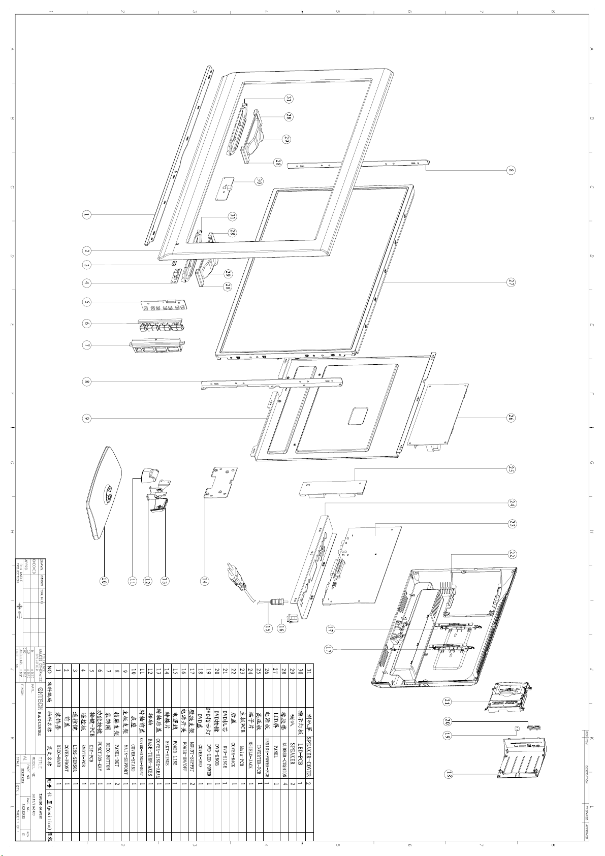
Exploded view
:
IC Introduction
Detailed Circuit
Components List
Debug Instruction
◆
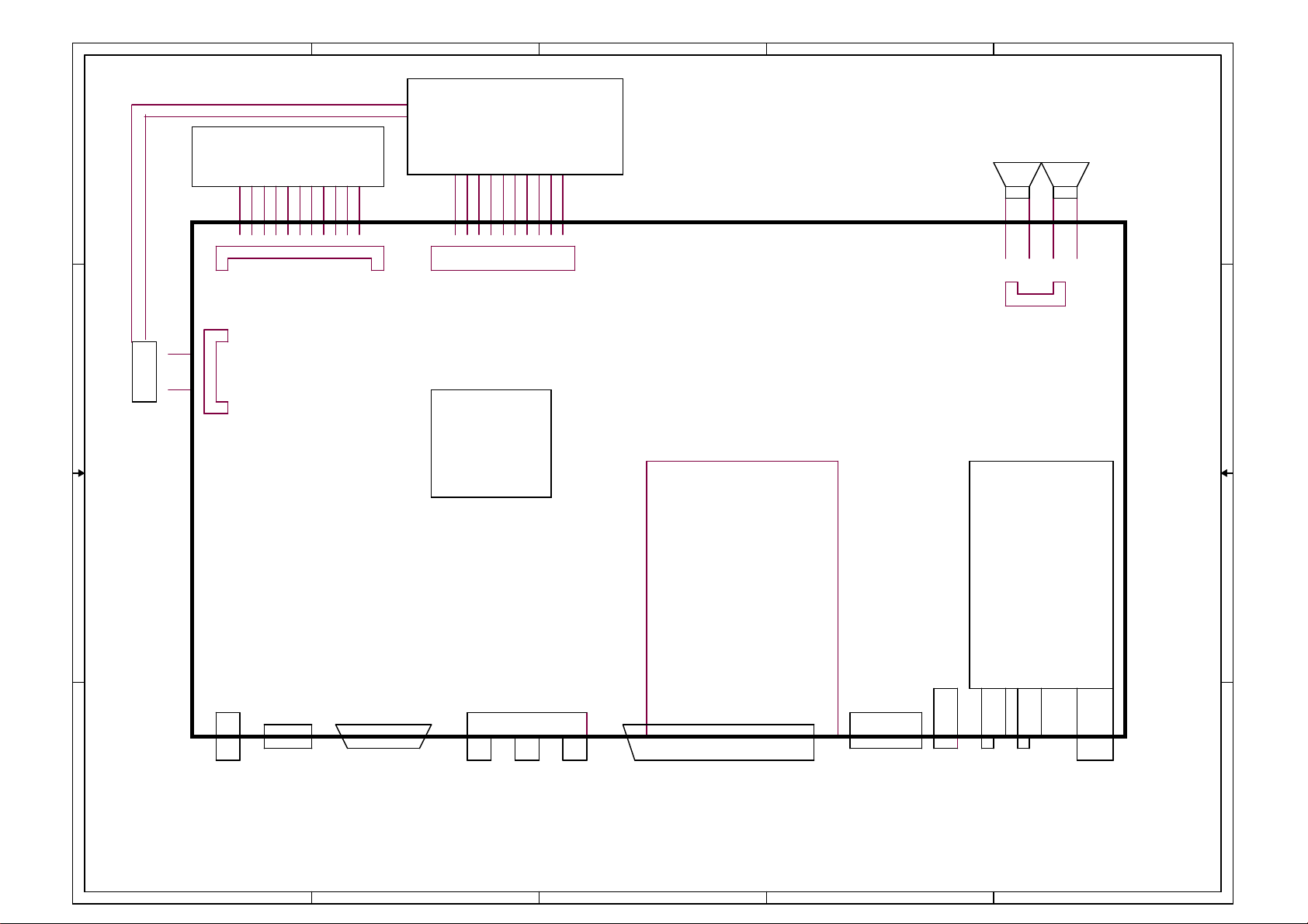
Schematic Diagram Block
◆
Printed Circuit
Part1:
5
4
3
2
1
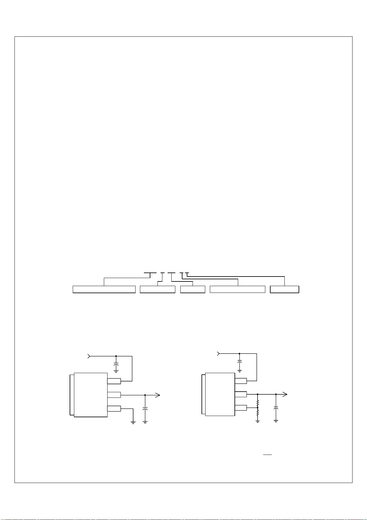
Schematic Diagram
PANEL
D D
KEY&IR BOARD
J3
KEY&IR CONNECTOR
CON8 J14
5V IR GND K0 R G GND K1 K2 K3 K4 K5 K6 K7
C C
INVERTER BOARD
J4
INVERTER CONNECTOR
12V 12V EN ADJ GND GND
B B
LVDS CONNECTOR
SPV7100
AMPLIFER CONNECTOR
GND R GND L
A A
HDMI PC AV
YUV
5
4
SCART SVHS
PCMCIA
3
USB
2
PC
AUDIO
IN
Earphone
TUNER
1
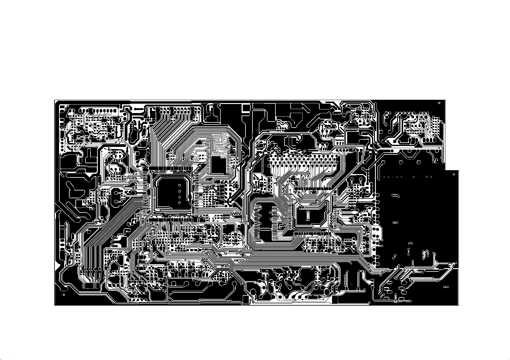
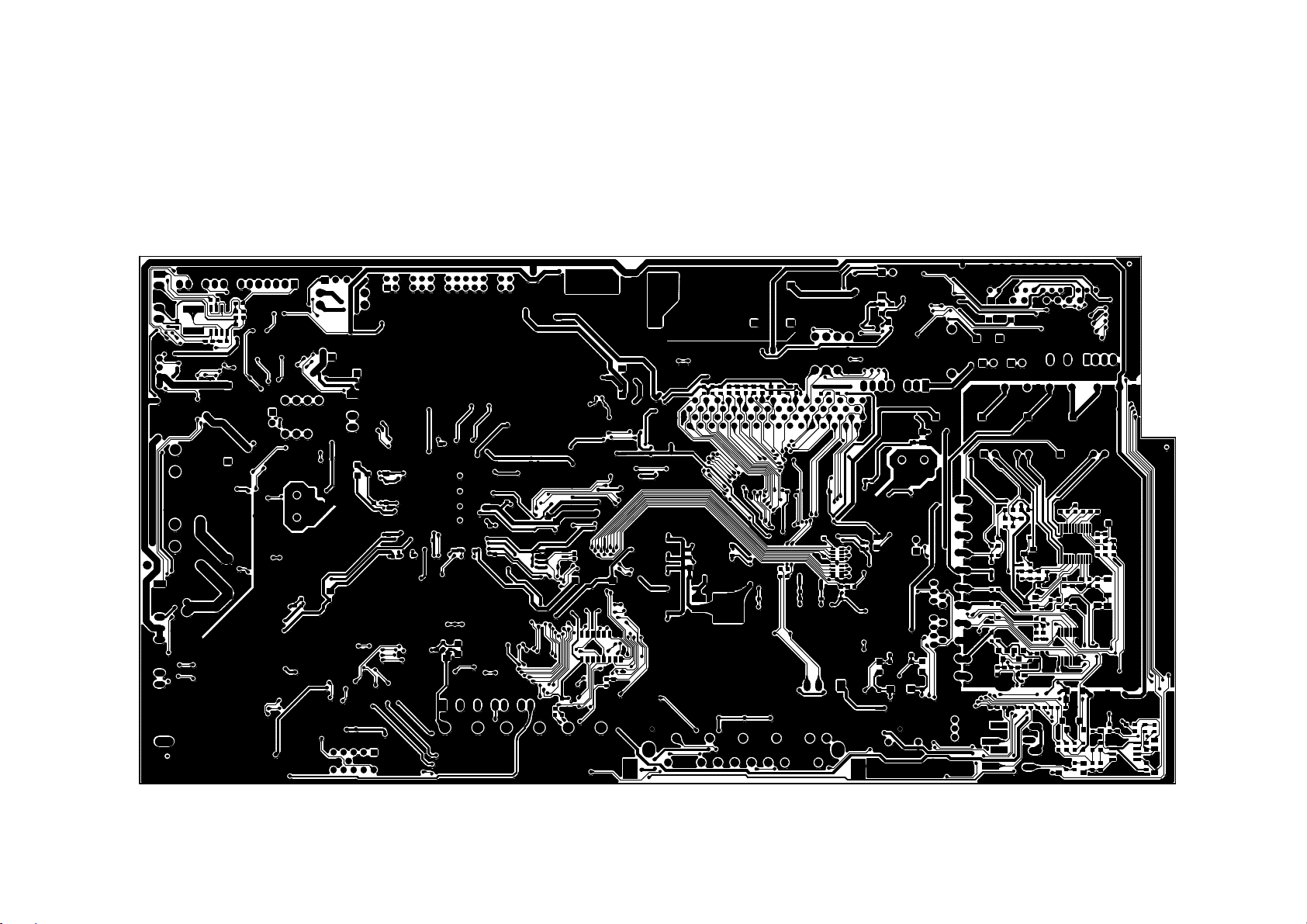
Printed Circuit
TV Main Board (Top View)
TV Main Board
(Bottom view)
Part3:
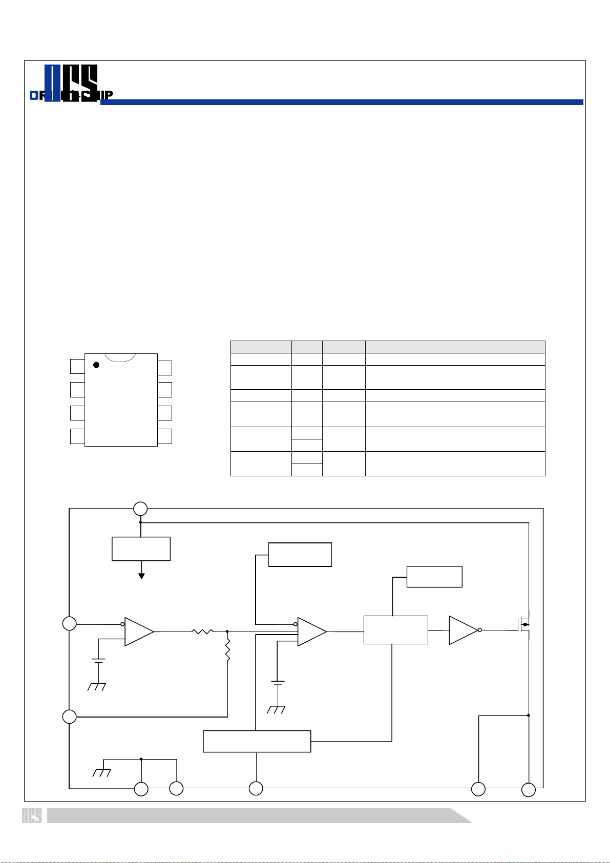
IC Introduction
SWITCHING BUCK REGULATOR
OCP2030
General Description
The OCP2030 is a buck topology of switching regulator for wide operating voltage applications field. The OCP2030
includes a high current P-MOSFET, high precision reference (0.5V) for comparing output voltage with feedback
amplifier, an internal dead-time controller and oscillator for controlling the maximum duty cycle and PWM frequency,
and has power-on programmable soft start time and short circuit PMOS turn-off and auto re-start protection functions.
Features
z Precision feedback reference voltage: 0.5V (2%)
z Wide supply voltage operating range: 3.6 to 20V
z
Low current consumption: 3mA
z Internal fixed oscillator frequency: Typ. 360KHz
z Programmable Soft-Start function (SS)
z Short Circuit Shutdown and Auto Re-start function(ARSCP)
z Built-in P-MOSFET for 3A loading capability
z Package: SOP8
Pin Configuration
Top View
1
2
3
4
Block Diagram
8
7
OCP2030
6
5
1
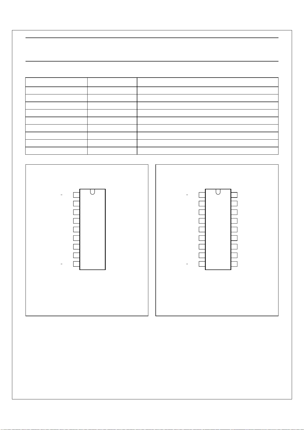
Name No. Status Description
VCC 1 P IC Power Supply (PMOS Source)
SS/SCP 2 I
IN- 3 I Error Amplifier Inverting Input
FB 4 O
GND
LX
5
6
7
8
P
O PMOS High Current Output
Connecting with a Soft-start &
ARSCP timing capacitor
Error Amplifier Compensation
Output
IC Ground
Reference
Regulator
1.25V
Oscillator
Therm al
Shuntdown
3
0.5V
36KΩ
500Ω
Output drive
control circuits
0.8V
4
Soft start&Auto Re-start
S.C.P Circuits
5
6
2
Page 1 - 9
7
Rev. 1.1 May.22, 2007
8
Philips Semiconductors Product data
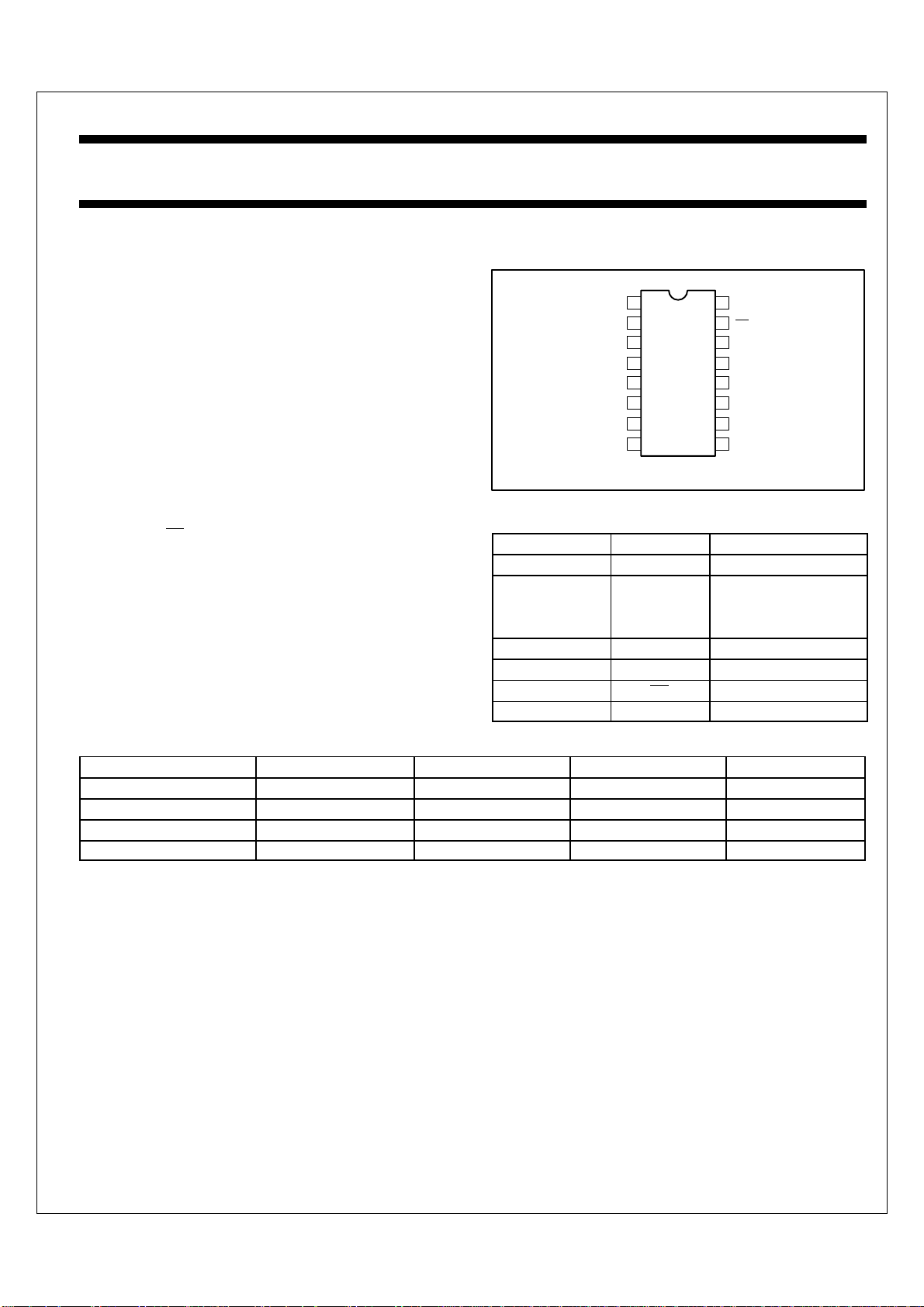
CBT3257Quad 1-of-2 multiplexer/demultiplexer
FEATURES
• 5 Ω switch connection between two ports
TTL-compatible input levels
•
•
Minimal propagation delay through the switch
•
Latch-up protection exceeds 500 mA per JESD78
•
ESD protection exceeds 2000 V HBM per JESD22-A114,
200 V MM per JESD22-A115 and 1000 V CDM per JESD22-C101
DESCRIPTION
The CBT3257 is a quad 1-of-2 high-speed TTL-compatible
multiplexer/demultiplexer. The low on resistance of the switch allows
inputs to be connected to outputs without adding propagation delay
or generating additional ground bounce noise.
Output Enable (OE
appropriate B1 and B2 outputs for the A-input data.
The CBT3257 is characterized for operation from -40 to +85 °C.
) and select-control (S) inputs select the
PIN CONFIGURATION
1
S
2
1B1
3
1B2
4
1A
5
2B1
6
2B2
7
2A
89
GND
16
15
14
13
12
11
10
SA00533
V
OE
4B1
4B2
4A
3B1
3B2
3A
CC
PIN DESCRIPTION
PIN NUMBER SYMBOL NAME AND FUNCTION
1 S Select-control input
2, 3,
5, 6,
10, 11,
13, 14
4, 7, 9, 12 1A, 2A, 3A, 4A A inputs
8 GND Ground (0 V)
15 OE Output enable
16 V
1B1, 1B2,
2B1, 2B2
3B1, 3B2
4B1, 4B2
CC
B outputs
Positive supply voltage
ORDERING INFORMATION
PACKAGES TEMPERATURE RANGE ORDER CODE TOPSIDE MARK DWG NUMBER
16-pin plastic SO -40 to 85 °C CBT3257D CBT3257D SOT109-1
16-pin plastic SSOP -40 to 85 °C CBT3257DB CT3257 SOT338-1
16-pin plastic SSOP (QSOP) -40 to 85 °C CBT3257DS CBT3257 SOT519-1
16-pin plastic TSSOP -40 to 85 °C CBT3257PW CBT3257 SOT403-1
Standard packing quantities and other packaging data is available at www.philipslogic.com/packaging.
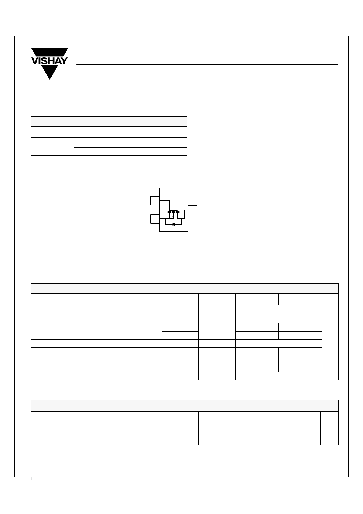
PRODUCT SUMMARY
V
b
b
VDS (V) r
-20
0.100 @ V
0.150 @ V
P-Channel 2.5-V (G-S) MOSFET
(W) ID (A)
DS(on)
= -4.5 V -2.4
GS
= -2.5 V -2.0
GS
G
1
S
2
b
TO-236
(SOT-23)
D
3
Ordering Information: Si2301BDS-T1
Si2301BDS
Vishay Siliconix
Top View
Si2301 BDS (L1)*
*Marking Code
ABSOLUTE MAXIMUM RATINGS (TA = 25_C UNLESS OTHERWISE NOTED)
Parameter Symbol 5 sec Steady State Unit
Drain-Source Voltage V
Gate-Source Voltage V
Continuous Drain Current (TJ = 150_C)
Pulsed Drain Current
Continuous Source Current (Diode Conduction)
Power Dissipation
Operating Junction and Storage Temperature Range TJ, T
a
_
b
TA= 25_C
TA= 70_C
TA= 25_C
TA= 70_C
DS
GS
I
D
I
DM
I
S
P
D
stg
-2.4 -2.2
-1.9 -1.8
-0.72 -0.6
0.9 0.7
0.57 0.45
-55 to 150 _C
THERMAL RESISTANCE RATINGS
-20
"8
-10
A
W
Parameter Symbol Typical Maximum Unit
Maximum Junction-to-Ambient
Maximum Junction-to-Ambient
Notes
a. Pulse width limited by maximum junction temperature.
b. Surface Mounted on FR4 Board, t v 5 sec.
c. Surface Mounted on FR4 Board.
b
R
c
thJA
120 145
140 175
_C/W
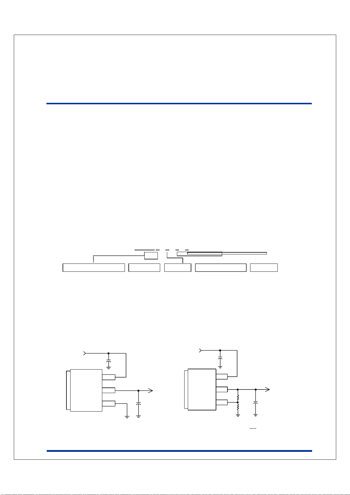
5A Low Dropout Positive Adjustable or Fixed-Mode Regulator
Features
1.4V maximum dropout at full load current
•
•
Built-in thermal shutdown
•
Output current limiting
•
Adjustable output voltage or fixed 1.5V, 1.8V, 2.5V,
3.3V, 5.0V
•
Fast transient response
Good noise rejection
•
Package : TO252, TO263, TO220
•
General Description
AP1084 is a low dropout positive adjustable or fixedmode regulator with minimum of 5.0A output current
capability. The product is specifically designed to
provide well-regulated supply for low voltage IC
applications such as high-speed bus termination and
low current 3.3V logic supply. AP1084 is also well
suited for other applications such as VGA cards.
AP1084 is guaranteed to have lower than 1.4V
dropout at full load current making it ideal to provide
well-regulated outputs of 1.25 to 3.3V with 4.7 to
12V input supply.
Ordering Information
AP1084 X X X X
AP1084
Low Dropout Regulator Package Vout
Typical Circuit
5.0V to 3.3V Fixed Mode Regulator
5V
Tab is Vout
Vin
Vout
GND
C1
100uF
D : TO252-3L
K : TO263-3L
T : TO220-3L
3.3V/5A
C2
100uF
Blank : Adj
15 = 1.5V
18 = 1.8V
25 = 2.5V
33 = 3.3V
50 = 5.0V
Lead Free
Blank : Normal
L : Lead Free Package
Adjustable Regulator
5V
Vin
Vout
Adj
Tab is Vout
C1
100uF
Note:
Packing
Blank : Tube
A : Taping
2.5V/5A
Ω
121
121
(1VV +∗=
C2
100uF
Ω
R
2
)
R
1
R1
R2
REFo
1A Low Dropout Positive Adjustable or Fixed-Mode Regulator
Features
- 1.4V maximum dropout at full load current
- Fast transient response
- Output current limiting
- Built-in thermal shutdown
- Packages: SOT223, TO263, TO252, TO220,
SOT89
- Good noise rejection
- 3-Terminal Adjustable or Fixed 1.5V, 1.8V, 1.9V,
2.5V, 3.3V, 5.0V
Applications
- PC peripheral
- Communication
General Description
AP1117 is a low dropout positive adjustable or
fixed-mode regulator with minimum of 1A output
current capability. The product is specifically
designed to provide well-regulated supply for low
voltage IC applications such as high-speed bus
termination and low current 3.3V logic supply.
AP1117 is also well suited for other applications
such as VGA cards. AP1117 is guaranteed to have
lower than 1.4V dropout at full load current making
it ideal to provide well-regulated outputs of 1.25 to
5.0 with 6.4V to 12V input supply.
Ordering Information
AP 1117 X XX X X
AP1117
Low Dropout Regulator
Typical Circuit
5V
Tab is Vout
( 5V/3.3V fixed output )
Vin
Vout
GND
C1
100uF
Package Vout
E : SOT223-3L
K : TO263-3L
D : TO252-3L
T : TO220-3L
Y : SOT89-3L
C2
100uF
Blank : ADJ
15 : 1.5V
18 : 1.8V
19: 1.9V
25 : 2.5V
33 : 3.3V
50 : 5.0V
3.3V/1A
Lead Free
Blank : Normal
L : Lead Free Package
5V
Vout
Tab is Vout
C1
100uF
Vin
Adj
( 5V/2.5V ADJ output )
Note:
(1 VV +∗=
REFo
Blank : Tube
A : Taping
R1
121
Ω
R2
Ω
121
R
2
)
R
1
Packing
V
o
2.5V/1A
C2
100uF
AP9435M
Advanced Power
Electronics Corp.
▼
▼ Simple Drive Requirement
▼ ▼
▼
▼ Low On-resistance
▼ ▼
▼
▼ Fast Switching
▼ ▼
D
D
D
SO-8
D
P-CHANNEL ENHANCEMENT MODE
POWER MOSFET
G
S
S
S
Description
The Advanced Power MOSFETs from APEC provide the
designer with the best combination of fast switching,
ruggedized device design, low on-resistance and cost-effectiveness.
The SO-8 package is universally preferred for all commercial-industrial
surface mount applications and suited for low voltage applications
such as DC/DC converters.
BV
R
DS(ON)
I
D
G
DSS
-30V
50mΩ
-5.3A
D
S
Absolute Maximum Ratings
Symbol Units
V
DS
V
GS
=25℃ A
I
D@TA
I
=70℃ A
D@TA
I
DM
PD@TA=25℃ W
Drain-Source Voltage
Gate-Source Voltage
Continuous Drain Current
Continuous Drain Current
Pulsed Drain Current
Total Power Dissipation 2.5
Linear Derating Factor 0.02
T
STG
T
J
Storage Temperature Range
Operating Junction Temperature Range -55 to 150
Parameter
3
3
1
Rating
-30
± 20
-5.3
-4.7
-20
-55 to 150
V
V
A
W/℃
℃
℃
Thermal Data
Symbol Value Unit
Rthj-amb Thermal Resistance Junction-ambient
Parameter
3
Max. 50 ℃/W

2N7000 / 2N7002 / NDS7002A
N-Channel Enhancement Mode Field Effect Transistor
General Description Features
November 1995
These N-Channel enhancement mode field effect transistors
are produced using Fairchild's proprietary, high cell density,
DMOS technology. These products have been designed to
minimize on-state resistance while provide rugged, reliable,
and fast switching performance. They can be used in most
applications requiring up to 400mA DC and can deliver
High density cell design for low R
Voltage controlled small signal switch.
Rugged and reliable.
High saturation current capability.
DS(ON)
.
pulsed currents up to 2A. These products are particularly
suited for low voltage, low current applications such as small
servo motor control, power MOSFET gate drivers, and other
switching applications.
___________________________________________________________________________________________
D
S
Units
V
G
S
TO-92
2N7000
D
Absolute Maximum Ratings
Symbol Parameter
V
DSS
V
DGR
V
GSS
I
D
P
D
T
J,TSTG
T
L
THERMAL CHARACTERISTICS
R
JA
θ
Drain-Source Voltage 60 V
Drain-Gate Voltage (RGS < 1 MΩ)
Gate-Source Voltage - Continuous
- Non Repetitive (tp < 50µs)
Maximum Drain Current - Continuous 200 115 280 mA
Maximum Power Dissipation 400 200 300 mW
Derated above 25oC 3.2 1.6 2.4 mW/°C
Operating and Storage Temperature Range -55 to 150 -65 to 150 °C
Maximum Lead Temperature for Soldering
Purposes, 1/16" from Case for 10 Seconds
Thermal Resistance, Junction-to-Ambient 312.5 625 417 °C/W
G
(TO-236AB)
2N7002/NDS7002A
TA = 25°C unless otherwise noted
2N7000 2N7002 NDS7002A
60 V
20
±
40
±
- Pulsed 500 800 1500
300 °C
Philips Semiconductors Product specification
2 × 6 W stereo power amplifier TDA1517; TDA1517P
FEATURES
• Requires very few external components
• High output power
• Fixed gain
• Good ripple rejection
GENERAL DESCRIPTION
The TDA1517 is an integrated class-B dual output
amplifier in a plastic single in-line medium power package
with fin (SIL9MPF) and a plastic heat-dissipating dual
in-line package (HDIP18). The device is primarily
developed for multi-media applications.
• Mute/standby switch
• AC and DC short-circuit safe to ground and V
P
• Thermally protected
• Reverse polarity safe
• Capability to handle high energy on outputs (VP=0V)
• No switch-on/switch-off plop
• Electrostatic discharge protection.
QUICK REFERENCE DATA
SYMBOL PARAMETER CONDITIONS MIN. TYP. MAX. UNIT
V
P
I
ORM
I
q(tot)
I
sb
I
sw
|Z
| input impedance 50 −−kΩ
I
P
o
supply voltage 6.0 14.4 18.0 V
repetitive peak output current −−2.5 A
total quiescent current − 40 80 mA
standby current − 0.1 100 µA
switch-on current −−40 µA
output power RL=4Ω; THD = 0.5% − 5 − W
R
=4Ω; THD = 10% − 6 − W
L
SVRR supply voltage ripple rejection fi= 100 Hz to 10 kHz 48 −−dB
α
cs
G
v
V
no(rms)
T
c
channel separation 40 −−dB
closed loop voltage gain 19 20 21 dB
noise output voltage (RMS value) − 50 −µV
crystal temperature −−150 °C
ORDERING INFORMATION
TYPE
NUMBER
NAME DESCRIPTION VERSION
PACKAGE
TDA1517 SIL9MPF plastic single in-line medium power package with fin; 9 leads SOT110-1
TDA1517P HDIP18 plastic heat-dissipating dual in-line package; 18 leads SOT398-1
Philips Semiconductors Product specification
2 × 6 W stereo power amplifier TDA1517; TDA1517P
PINNING
SYMBOL PIN DESCRIPTION
−INV1 1 non-inverting input 1
SGND 2 signal ground
SVRR 3 supply voltage ripple rejection output
OUT1 4 output 1
PGND 5 power ground
OUT2 6 output 2
V
P
M/SS 8 mute/standby switch input
−INV2 9 non-inverting input 2
7 supply voltage
dbook, halfpage
INV1
SGND
SVRR
OUT1
PGND
OUT2
V
M/SS
INV2
1
2
3
4
TDA1517
5
6
7
P
8
9
MLC352
Fig.2 Pin configuration for SOT110-1.
FUNCTIONAL DESCRIPTION
The TDA1517 contains two identical amplifiers with
differential input stages. The gain of each amplifier isfixed
at 20 dB. A special feature of the device is the
mute/standby switch which has the following features:
• Low standby current (<100 µA)
• Low mute/standby switching current
• Mute condition.
(low cost supply switch)
dbook, halfpage
Pins 10 to 18 should be connected to GND or floating.
INV1
SGND
SVRR
OUT1
PGND
OUT2
V
M/SS
INV2
1
2
3
4
TDA1517P
5
6
7
P
8
9
18
17
16
15
14
13
12
11
10
MLC353
Fig.3 Pin configuration for SOT398-1.
Fremont Micro Devices, Inc.
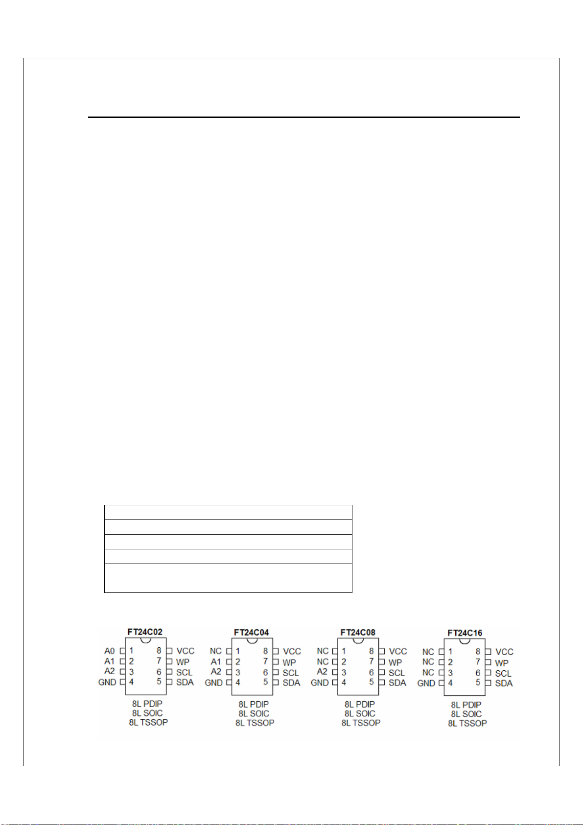
FEATURES
Low voltage and low power operati ons:
• FT24C02/04/08/16: V
• FT24C02A/04A/08A/16A: VCC = 1.8V to 5.5V
Maximum Standby current < 1µA (typically 0.02µA and 0.06µA @ 1.8V and 5.5V respectively).
16 bytes page write mode.
Partial page write operation allowed.
Internally organized: 256 × 8 (2K), 512 × 8 (4K), 1024 × 8 (8K), 2048 × 8 (16K).
Standard 2-wire bi-directional serial interface.
Schmitt trigger, filtered inputs for noise protection.
Self-timed programming cycle (5ms maximum).
Automatic erase before write operation.
Write protect pin for hardware data protection.
High reliability: typically 800,000 cycles endurance.
100 years data retention.
Industrial temperature range (-40o C to 85o C).
Standard 8-pin PDIP/SOIC/TSSOP Pb-free packages.
CC
FT24C02 / 04 / 08 / 16
FT24C02A / 04A / 08A / 16A
= 2.5V to 5.5V
and
DESCRIPTION
The FT24C02/04/08/16 series are 2048/4096/8192/16384 bits of serial Electrical Erasable and
Programmable Read Only Memory, commonly known as EEPROM. They are organized as
256/512/1024/2048 words of 8 bits (1 byte) each. The devices are fabricated with proprietary
advanced CMOS process for low power and low voltage applications. These devices are available in
standard 8-lead PDIP, 8-lead JEDEC SOIC and 8-lead TSSOP packages. A standard 2-wire serial
interface is used to address all read and write functions. Our extended V
devices enables wide spectrum of applications.
range (1.8V to 5.5V)
CC
PIN CONFIGURATION
Pin Name Pin Function
A2, A1, A0 Device Address Inputs
SDA Serial Data Input / Open Drain Output
SCL Serial Clock Input
WP Write Protect
NC No-Connect
All three packaging types come in conventional or Pb-free certified.
HY5DU281622FT(P) Series
DESCRIPTION
The HY5DU281622FT(P) is a 134,217,728-bit CMOS Double Data R ate (D DR) Synchronous DRAM, ideally suited for the
main memory applications which requires large memory density and high bandwidth.
This Hynix 128Mb DDR SDRAMs offer fully synchronous operations referenced to both rising and falling edges of the
clock. While all addresses and control inputs are latched on the rising edges of the CK (fal ling edges of the /CK), Data,
Data strobes and Write data masks inputs are sampled on both rising and falling edges of it. The data paths are internally pipelined and 2-bit prefetched to achieve very high ban dwid th. All inp ut a nd output voltage levels are compatible
with SSTL_2.
FEATURES
•VDD, V
DDQ
= 2.3V
min
~ 2.7V
max
(Typical 2.5V Operation +/- 0.2V for DDR266, 333)
•VDD, V
DDQ
= 2.4V
min
~ 2.7V
max
(Typical 2.6V Operation +0.1/- 0.2V for DDR400
and 400Mbps/pin product)
• All inputs and outputs are compatible with SSTL_2
interface
• Fully differential clock inputs (CK, /CK) operation
• Double data rate interface
• Source synchronous - data transaction aligned to
bidirectional data strobe (DQS)
• x16 device has two bytewide data strobes (UDQS,
LDQS) per each x8 I/O
• Data outputs on DQS edges when read (edged DQ)
Data inputs on DQS centers when write (centered
DQ)
• On chip DLL align DQ and DQS transition with CK
transition
• DM mask write data-in at the both rising and falling
edges of the data strobe
• All addresses and control inputs except data, data
strobes and data masks latched on the rising edges
of the clock
• Programmable CAS latency 2/2.5 (DDR266, 333)
and 3 (DDR400 and 400Mbps/pin product) supported
• Programmable burst length 2/4/8 with both sequential and interleave mode
• Internal four bank operations with single pulsed
/RAS
• Auto refresh and self refresh supported
lock out function supported
RAS
•t
• 4096 refresh cycles/64ms
• JEDEC standard 400mil 66pin TSOP-II with 0.65mm
pin pitch
• Lead free (*ROHS Compliant)
ORDERING INFORMATION
Part No. Configuration Package
400mil
HY5DU281622F(L)TP-X* 8Mx16
* X means speed grade
** Lead-free product
*ROHS (Restriction Of Hazardous Substances)
Rev. 0.03 /Jun. 2006 3
66pin
TSOP-II**
OPERATING FREQUENCY
Grade Clock Rate Remark
-5 200MHz@CL3
-D43 200MHz@CL3 DDR400B (3-3-3)
-D4 200MHz@CL3 DDR400 (3-4-4)
- J 133MHz@CL2
- K 133MHz@CL2 133MHz@CL2.5 DDR266A (2-3-3)
- H 100MHz@CL2 133MHz@CL2.5 DDR266B (2.5-3-3)
166MHz @CL2.5
& @CL3
400Mbps/pin (maxi-
mum Date rate)
DDR333 (2.5-3-3)
DDR333 (3-3-3)

PIN CONFIGURATION
HY5DU281622FT(P) Series
V
DD
DQ0
V
DDQ
DQ1
DQ2
V
SSQ
DQ3
DQ4
V
DDQ
DQ5
DQ6
V
SSQ
DQ7
NC
V
DDQ
LDQ S
NC
V
DD
NC
LDM
/W E
/CAS
/RA S
/CS
NC
BA0
BA1
A10/AP
A0
A1
A2
A3
DD
V
10
11
12
13
14
15
16
17
18
19
20
21
22
23
24
25
26
27
28
29
30
31
32
33
1
2
3
4
5
6
7
8
9
400mil x 875m il
66pin TSOP-II
0.65mm pin pitch
66
65
64
63
62
61
60
59
58
57
56
55
54
53
52
51
50
49
48
47
46
45
44
43
42
41
40
39
38
37
36
35
34
V
SS
DQ15
V
SSQ
DQ14
DQ13
V
DDQ
DQ12
DQ11
V
SSQ
DQ10
DQ9
V
DDQ
DQ8
NC
V
SSQ
UDQS
NC
VREF
V
SS
UDM
/CK
CK
CKE
NC
NC
A11
A9
A8
A7
A6
A5
A4
SS
V
ROW AND COLUMN ADDRESS INFORMATION
• Organization : 2M x 16 x 4banks
• Row Address : A0 - A11
• Column Address : A0 - A8
• Bank Address : BA0, BA1
• Auto Precharge Flag : A10
• Refresh : 4K
Rev. 0.03 /Jun. 2006 4
MODEL:CDT-9DT33C-00
DEFINITION OF TERMINALS / SUPPLY DATA
CDT-9DT33C-00,CDT-9DT23C-00 , CDT-9DT13C-00
.
11109
Terminal Function Remark
1 DC-power option for tuners with P-extension Max. permissible current: 100mA
.
71
8
3
5
2
4
6
.
.
2
External RF-gain control voltage (0.5V -
4.0V)
Source impedance limited to 1kohms
3 PLL chip address select (I2C / tuner) see application notes
4 SCL (I2C / tuner)
5 SDA (I2C / tuner)
6 4MHz reference frequency output; AC coupled
7
+5V r 5% supply tuner (VTU)
8 'broadband' IF - output AC coupled
max. gain at 3V
9 IF-gain control voltage
min. gain at 0V
(see application notes)
10 'narrowband' IF - output AC coupled
11 'narrowband' IF - output AC coupled
4
 Loading...