

Page 1

INDEX:
LH216S92DT SERVICE MANUAL
PART 1:
PART 2:
PART 3
PART 4:
PART 5:
PART6:
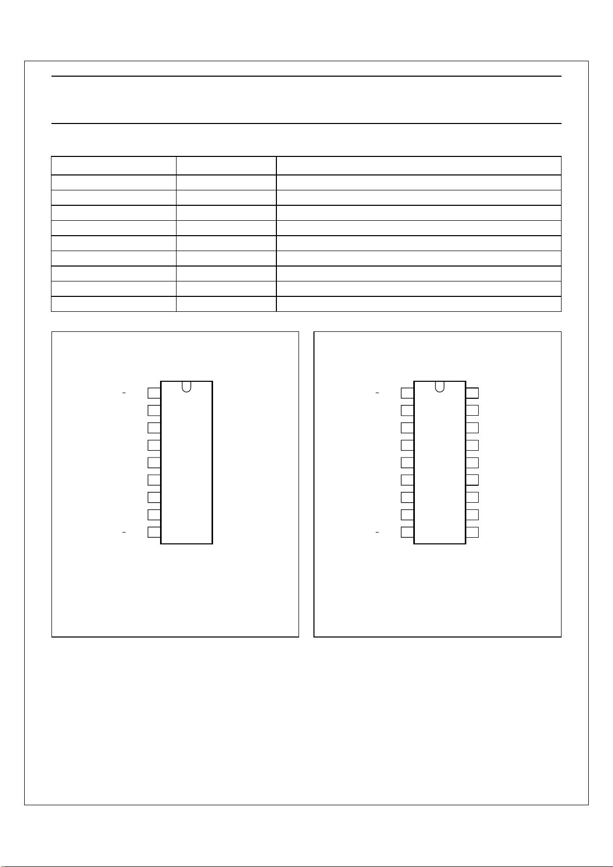
Brief Introduction Of The LH216S92DT
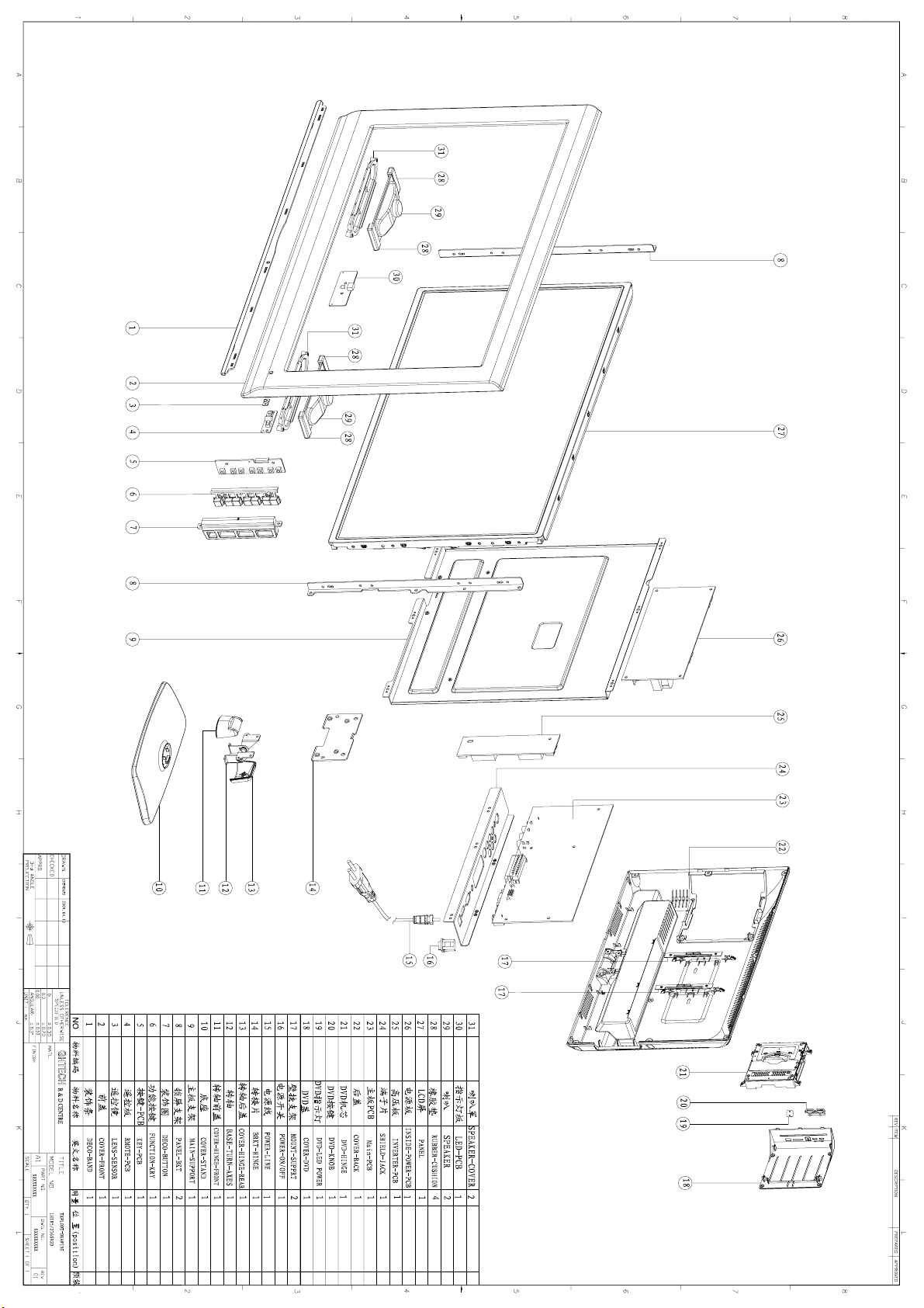
Exploded view
:
IC Introduction
Detailed Circuit
Components List
Debug Instruction
◆
Schematic Diagram Block
◆
Printed Circuit
Page 2
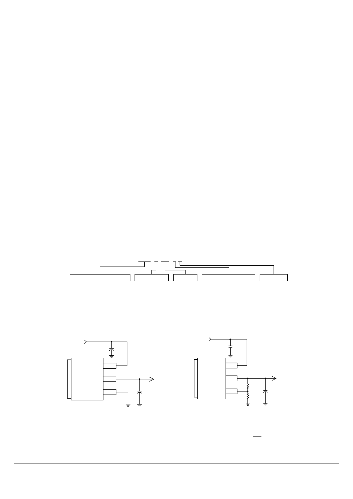
Part1:
5
4
3
2
1
Schematic Diagram
PANEL
D D
KEY&IR BOARD
J3
KEY&IR CONNECTOR
CON8 J14
5V IR GND K0 R G GND K1 K2 K3 K4 K5 K6 K7
C C
INVERTER BOARD
J4
INVERTER CONNECTOR
12V 12V EN ADJ GND GND
B B
LVDS CONNECTOR
SPV7100
AMPLIFER CONNECTOR
GND R GND L
A A
HDMI PC AV
YUV
5
4
SCART SVHS
PCMCIA
3
USB
2
PC
AUDIO
IN
Earphone
TUNER
1
Page 3
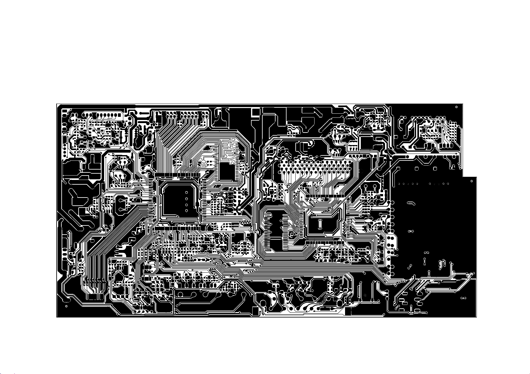
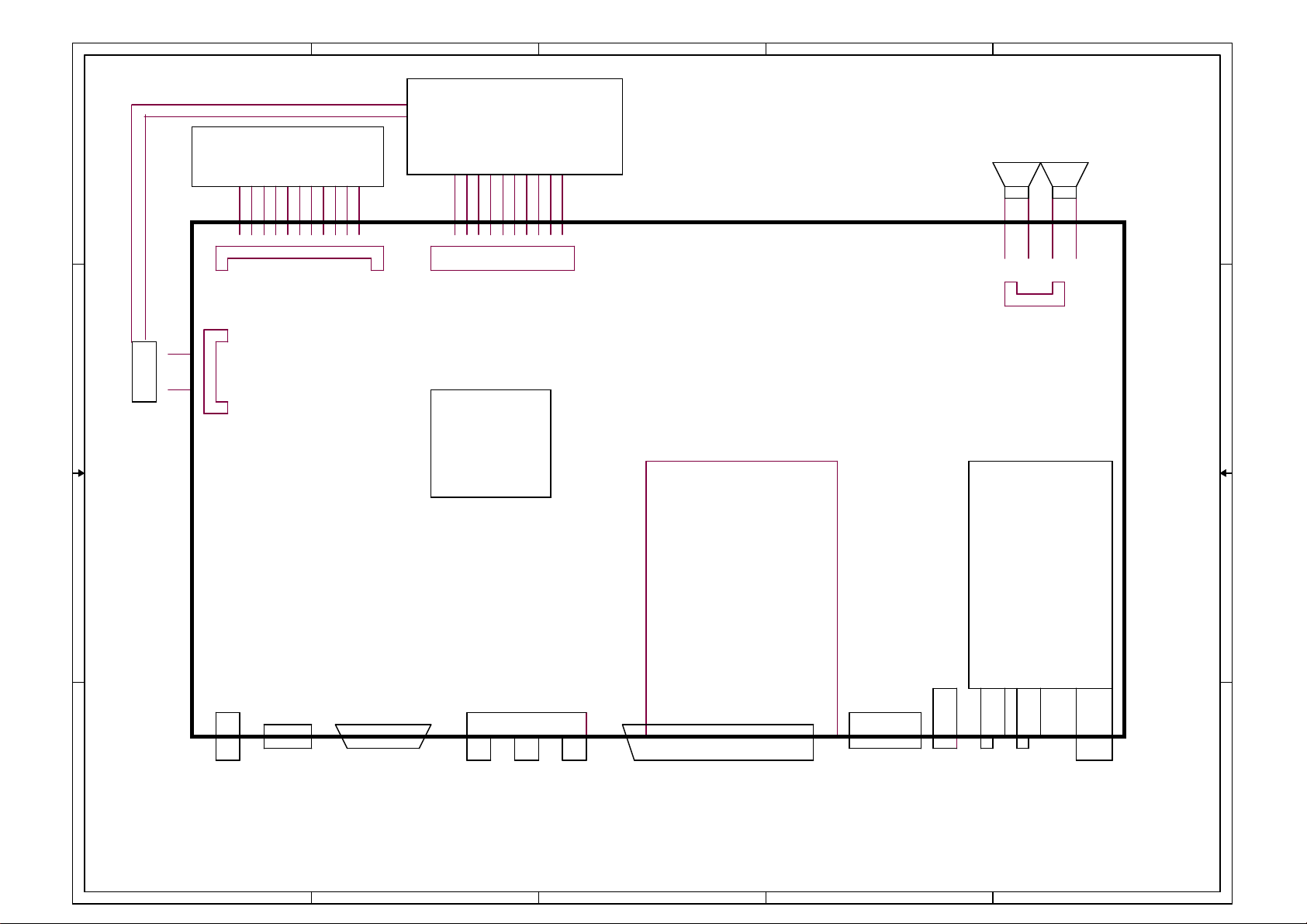
Printed Circuit
TV Main Board (Top View)
Page 4
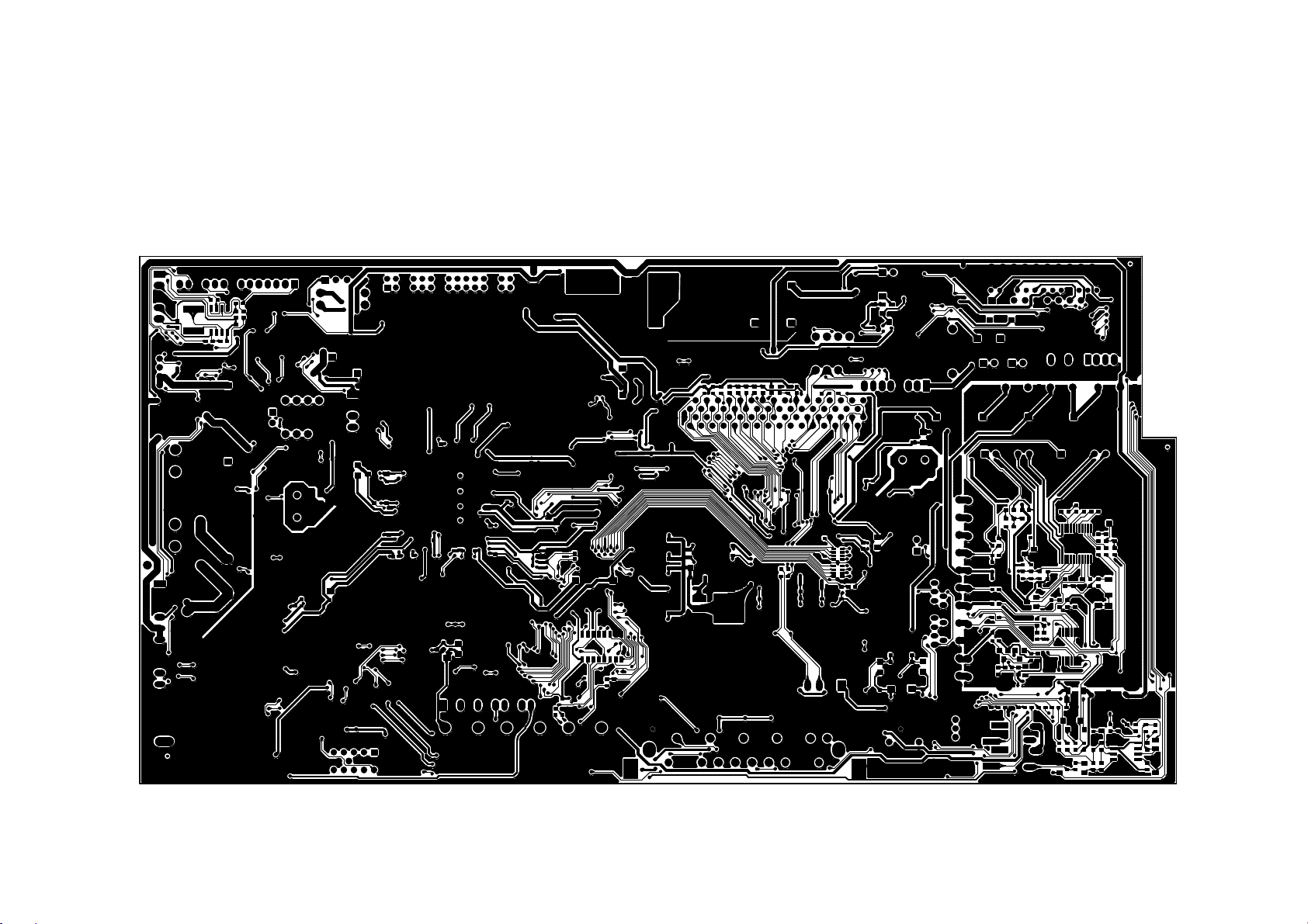
TV Main Board
(Bottom view)
Page 5
Page 6
Part3:
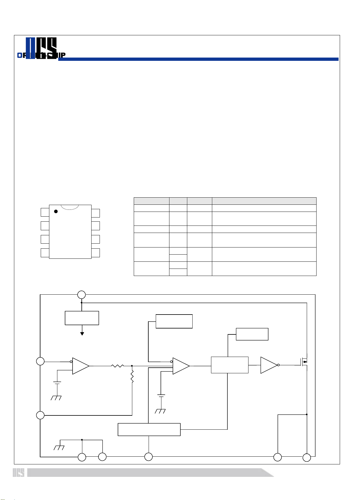
IC Introduction
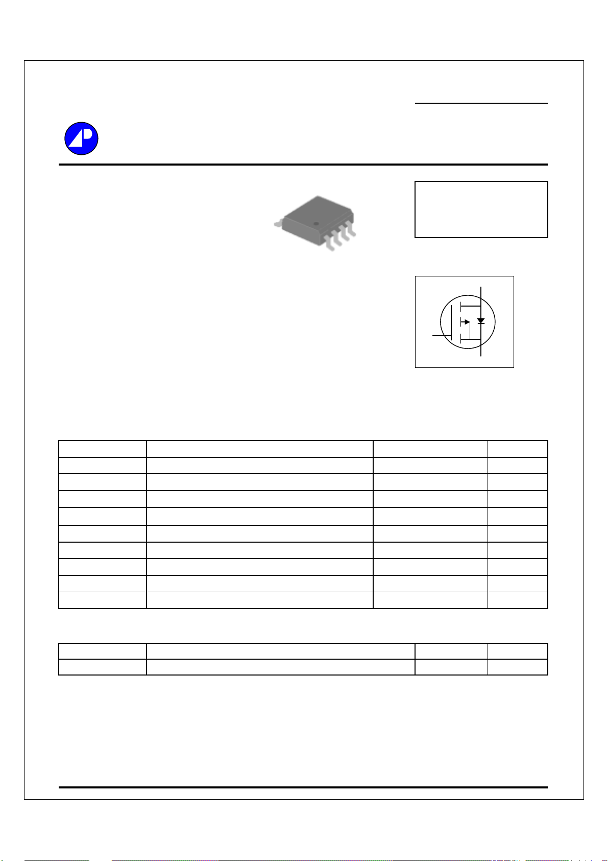
SWITCHING BUCK REGULATOR
OCP2030
General Description
The OCP2030 is a buck topology of switching regulator for wide operating voltage applications field. The OCP2030
includes a high current P-MOSFET, high precision reference (0.5V) for comparing output voltage with feedback
amplifier, an internal dead-time controller and oscillator for controlling the maximum duty cycle and PWM frequency,
and has power-on programmable soft start time and short circuit PMOS turn-off and auto re-start protection functions.
Features
z Precision feedback reference voltage: 0.5V (2%)
z Wide supply voltage operating range: 3.6 to 20V
z
Low current consumption: 3mA
z Internal fixed oscillator frequency: Typ. 360KHz
z Programmable Soft-Start function (SS)
z Short Circuit Shutdown and Auto Re-start function(ARSCP)
z Built-in P-MOSFET for 3A loading capability
z Package: SOP8
Pin Configuration
Top View
1
2
3
4
Block Diagram
8
7
OCP2030
6
5
1
Name No. Status Description
VCC 1 P IC Power Supply (PMOS Source)
SS/SCP 2 I
IN- 3 I Error Amplifier Inverting Input
FB 4 O
GND
LX
5
6
7
8
P
O PMOS High Current Output
Connecting with a Soft-start &
ARSCP timing capacitor
Error Amplifier Compensation
Output
IC Ground
Reference
Regulator
1.25V
Oscillator
Therm al
Shuntdown
3
0.5V
36KΩ
500Ω
Output drive
control circuits
0.8V
4
Soft start&Auto Re-start
S.C.P Circuits
5
6
2
Page 1 - 9
7
Rev. 1.1 May.22, 2007
8
Page 7
Philips Semiconductors Product data
CBT3257Quad 1-of-2 multiplexer/demultiplexer
FEATURES
• 5 Ω switch connection between two ports
TTL-compatible input levels
•
•
Minimal propagation delay through the switch
•
Latch-up protection exceeds 500 mA per JESD78
•
ESD protection exceeds 2000 V HBM per JESD22-A114,
200 V MM per JESD22-A115 and 1000 V CDM per JESD22-C101
DESCRIPTION
The CBT3257 is a quad 1-of-2 high-speed TTL-compatible
multiplexer/demultiplexer. The low on resistance of the switch allows
inputs to be connected to outputs without adding propagation delay
or generating additional ground bounce noise.
Output Enable (OE
appropriate B1 and B2 outputs for the A-input data.
The CBT3257 is characterized for operation from -40 to +85 °C.
) and select-control (S) inputs select the
PIN CONFIGURATION
1
S
2
1B1
3
1B2
4
1A
5
2B1
6
2B2
7
2A
89
GND
16
15
14
13
12
11
10
SA00533
V
OE
4B1
4B2
4A
3B1
3B2
3A
CC
PIN DESCRIPTION
PIN NUMBER SYMBOL NAME AND FUNCTION
1 S Select-control input
2, 3,
5, 6,
10, 11,
13, 14
4, 7, 9, 12 1A, 2A, 3A, 4A A inputs
8 GND Ground (0 V)
15 OE Output enable
16 V
1B1, 1B2,
2B1, 2B2
3B1, 3B2
4B1, 4B2
CC
B outputs
Positive supply voltage
ORDERING INFORMATION
PACKAGES TEMPERATURE RANGE ORDER CODE TOPSIDE MARK DWG NUMBER
16-pin plastic SO -40 to 85 °C CBT3257D CBT3257D SOT109-1
16-pin plastic SSOP -40 to 85 °C CBT3257DB CT3257 SOT338-1
16-pin plastic SSOP (QSOP) -40 to 85 °C CBT3257DS CBT3257 SOT519-1
16-pin plastic TSSOP -40 to 85 °C CBT3257PW CBT3257 SOT403-1
Standard packing quantities and other packaging data is available at www.philipslogic.com/packaging.
Page 8
PRODUCT SUMMARY
V
b
b
VDS (V) r
-20
0.100 @ V
0.150 @ V
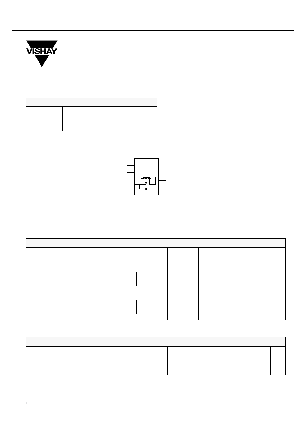
P-Channel 2.5-V (G-S) MOSFET
(W) ID (A)
DS(on)
= -4.5 V -2.4
GS
= -2.5 V -2.0
GS
G
1
S
2
b
TO-236
(SOT-23)
D
3
Ordering Information: Si2301BDS-T1
Si2301BDS
Vishay Siliconix
Top View
Si2301 BDS (L1)*
*Marking Code
ABSOLUTE MAXIMUM RATINGS (TA = 25_C UNLESS OTHERWISE NOTED)
Parameter Symbol 5 sec Steady State Unit
Drain-Source Voltage V
Gate-Source Voltage V
Continuous Drain Current (TJ = 150_C)
Pulsed Drain Current
Continuous Source Current (Diode Conduction)
Power Dissipation
Operating Junction and Storage Temperature Range TJ, T
a
_
b
TA= 25_C
TA= 70_C
TA= 25_C
TA= 70_C
DS
GS
I
D
I
DM
I
S
P
D
stg
-2.4 -2.2
-1.9 -1.8
-0.72 -0.6
0.9 0.7
0.57 0.45
-55 to 150 _C
THERMAL RESISTANCE RATINGS
-20
"8
-10
A
W
Parameter Symbol Typical Maximum Unit
Maximum Junction-to-Ambient
Maximum Junction-to-Ambient
Notes
a. Pulse width limited by maximum junction temperature.
b. Surface Mounted on FR4 Board, t v 5 sec.
c. Surface Mounted on FR4 Board.
b
R
c
thJA
120 145
140 175
_C/W
Page 9
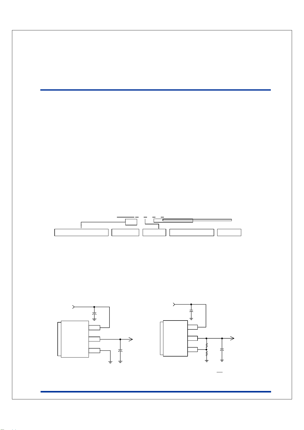
5A Low Dropout Positive Adjustable or Fixed-Mode Regulator
Features
1.4V maximum dropout at full load current
•
•
Built-in thermal shutdown
•
Output current limiting
•
Adjustable output voltage or fixed 1.5V, 1.8V, 2.5V,
3.3V, 5.0V
•
Fast transient response
Good noise rejection
•
Package : TO252, TO263, TO220
•
General Description
AP1084 is a low dropout positive adjustable or fixedmode regulator with minimum of 5.0A output current
capability. The product is specifically designed to
provide well-regulated supply for low voltage IC
applications such as high-speed bus termination and
low current 3.3V logic supply. AP1084 is also well
suited for other applications such as VGA cards.
AP1084 is guaranteed to have lower than 1.4V
dropout at full load current making it ideal to provide
well-regulated outputs of 1.25 to 3.3V with 4.7 to
12V input supply.
Ordering Information
AP1084 X X X X
AP1084
Low Dropout Regulator Package Vout
Typical Circuit
5.0V to 3.3V Fixed Mode Regulator
5V
Tab is Vout
Vin
Vout
GND
C1
100uF
D : TO252-3L
K : TO263-3L
T : TO220-3L
3.3V/5A
C2
100uF
Blank : Adj
15 = 1.5V
18 = 1.8V
25 = 2.5V
33 = 3.3V
50 = 5.0V
Lead Free
Blank : Normal
L : Lead Free Package
Adjustable Regulator
5V
Vin
Vout
Adj
Tab is Vout
C1
100uF
Note:
Packing
Blank : Tube
A : Taping
2.5V/5A
Ω
121
121
(1VV +∗=
C2
100uF
Ω
R
2
)
R
1
R1
R2
REFo
Page 10
1A Low Dropout Positive Adjustable or Fixed-Mode Regulator
Features
- 1.4V maximum dropout at full load current
- Fast transient response
- Output current limiting
- Built-in thermal shutdown
- Packages: SOT223, TO263, TO252, TO220,
SOT89
- Good noise rejection
- 3-Terminal Adjustable or Fixed 1.5V, 1.8V, 1.9V,
2.5V, 3.3V, 5.0V
Applications
- PC peripheral
- Communication
General Description
AP1117 is a low dropout positive adjustable or
fixed-mode regulator with minimum of 1A output
current capability. The product is specifically
designed to provide well-regulated supply for low
voltage IC applications such as high-speed bus
termination and low current 3.3V logic supply.
AP1117 is also well suited for other applications
such as VGA cards. AP1117 is guaranteed to have
lower than 1.4V dropout at full load current making
it ideal to provide well-regulated outputs of 1.25 to
5.0 with 6.4V to 12V input supply.
Ordering Information
AP 1117 X XX X X
AP1117
Low Dropout Regulator
Typical Circuit
5V
Tab is Vout
( 5V/3.3V fixed output )
Vin
Vout
GND
C1
100uF
Package Vout
E : SOT223-3L
K : TO263-3L
D : TO252-3L
T : TO220-3L
Y : SOT89-3L
C2
100uF
Blank : ADJ
15 : 1.5V
18 : 1.8V
19: 1.9V
25 : 2.5V
33 : 3.3V
50 : 5.0V
3.3V/1A
Lead Free
Blank : Normal
L : Lead Free Package
5V
Vout
Tab is Vout
C1
100uF
Vin
Adj
( 5V/2.5V ADJ output )
Note:
(1 VV +∗=
REFo
Blank : Tube
A : Taping
R1
121
Ω
R2
Ω
121
R
2
)
R
1
Packing
V
o
2.5V/1A
C2
100uF
Page 11
AP9435M
Advanced Power
Electronics Corp.
▼
▼ Simple Drive Requirement
▼ ▼
▼
▼ Low On-resistance
▼ ▼
▼
▼ Fast Switching
▼ ▼
D
D
D
SO-8
D
P-CHANNEL ENHANCEMENT MODE
POWER MOSFET
G
S
S
S
Description
The Advanced Power MOSFETs from APEC provide the
designer with the best combination of fast switching,
ruggedized device design, low on-resistance and cost-effectiveness.
The SO-8 package is universally preferred for all commercial-industrial
surface mount applications and suited for low voltage applications
such as DC/DC converters.
BV
R
DS(ON)
I
D
G
DSS
-30V
50mΩ
-5.3A
D
S
Absolute Maximum Ratings
Symbol Units
V
DS
V
GS
=25℃ A
I
D@TA
I
=70℃ A
D@TA
I
DM
PD@TA=25℃ W
Drain-Source Voltage
Gate-Source Voltage
Continuous Drain Current
Continuous Drain Current
Pulsed Drain Current
Total Power Dissipation 2.5
Linear Derating Factor 0.02
T
STG
T
J
Storage Temperature Range
Operating Junction Temperature Range -55 to 150
Parameter
3
3
1
Rating
-30
± 20
-5.3
-4.7
-20
-55 to 150
V
V
A
W/℃
℃
℃
Thermal Data
Symbol Value Unit
Rthj-amb Thermal Resistance Junction-ambient
Parameter
3
Max. 50 ℃/W
Page 12
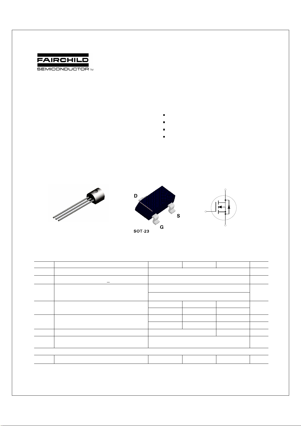
2N7000 / 2N7002 / NDS7002A
N-Channel Enhancement Mode Field Effect Transistor
General Description Features
November 1995
These N-Channel enhancement mode field effect transistors
are produced using Fairchild's proprietary, high cell density,
DMOS technology. These products have been designed to
minimize on-state resistance while provide rugged, reliable,
and fast switching performance. They can be used in most
applications requiring up to 400mA DC and can deliver
High density cell design for low R
Voltage controlled small signal switch.
Rugged and reliable.
High saturation current capability.
DS(ON)
.
pulsed currents up to 2A. These products are particularly
suited for low voltage, low current applications such as small
servo motor control, power MOSFET gate drivers, and other
switching applications.
___________________________________________________________________________________________
D
S
Units
V
G
S
TO-92
2N7000
D
Absolute Maximum Ratings
Symbol Parameter
V
DSS
V
DGR
V
GSS
I
D
P
D
T
J,TSTG
T
L
THERMAL CHARACTERISTICS
R
JA
θ
Drain-Source Voltage 60 V
Drain-Gate Voltage (RGS < 1 MΩ)
Gate-Source Voltage - Continuous
- Non Repetitive (tp < 50µs)
Maximum Drain Current - Continuous 200 115 280 mA
Maximum Power Dissipation 400 200 300 mW
Derated above 25oC 3.2 1.6 2.4 mW/°C
Operating and Storage Temperature Range -55 to 150 -65 to 150 °C
Maximum Lead Temperature for Soldering
Purposes, 1/16" from Case for 10 Seconds
Thermal Resistance, Junction-to-Ambient 312.5 625 417 °C/W
G
(TO-236AB)
2N7002/NDS7002A
TA = 25°C unless otherwise noted
2N7000 2N7002 NDS7002A
60 V
20
±
40
±
- Pulsed 500 800 1500
300 °C
Page 13
Philips Semiconductors Product specification
2 × 6 W stereo power amplifier TDA1517; TDA1517P
FEATURES
• Requires very few external components
• High output power
• Fixed gain
• Good ripple rejection
GENERAL DESCRIPTION
The TDA1517 is an integrated class-B dual output
amplifier in a plastic single in-line medium power package
with fin (SIL9MPF) and a plastic heat-dissipating dual
in-line package (HDIP18). The device is primarily
developed for multi-media applications.
• Mute/standby switch
• AC and DC short-circuit safe to ground and V
P
• Thermally protected
• Reverse polarity safe
• Capability to handle high energy on outputs (VP=0V)
• No switch-on/switch-off plop
• Electrostatic discharge protection.
QUICK REFERENCE DATA
SYMBOL PARAMETER CONDITIONS MIN. TYP. MAX. UNIT
V
P
I
ORM
I
q(tot)
I
sb
I
sw
|Z
| input impedance 50 −−kΩ
I
P
o
supply voltage 6.0 14.4 18.0 V
repetitive peak output current −−2.5 A
total quiescent current − 40 80 mA
standby current − 0.1 100 µA
switch-on current −−40 µA
output power RL=4Ω; THD = 0.5% − 5 − W
R
=4Ω; THD = 10% − 6 − W
L
SVRR supply voltage ripple rejection fi= 100 Hz to 10 kHz 48 −−dB
α
cs
G
v
V
no(rms)
T
c
channel separation 40 −−dB
closed loop voltage gain 19 20 21 dB
noise output voltage (RMS value) − 50 −µV
crystal temperature −−150 °C
ORDERING INFORMATION
TYPE
NUMBER
NAME DESCRIPTION VERSION
PACKAGE
TDA1517 SIL9MPF plastic single in-line medium power package with fin; 9 leads SOT110-1
TDA1517P HDIP18 plastic heat-dissipating dual in-line package; 18 leads SOT398-1
Page 14
Philips Semiconductors Product specification
2 × 6 W stereo power amplifier TDA1517; TDA1517P
PINNING
SYMBOL PIN DESCRIPTION
−INV1 1 non-inverting input 1
SGND 2 signal ground
SVRR 3 supply voltage ripple rejection output
OUT1 4 output 1
PGND 5 power ground
OUT2 6 output 2
V
P
M/SS 8 mute/standby switch input
−INV2 9 non-inverting input 2
7 supply voltage
dbook, halfpage
INV1
SGND
SVRR
OUT1
PGND
OUT2
V
M/SS
INV2
1
2
3
4
TDA1517
5
6
7
P
8
9
MLC352
Fig.2 Pin configuration for SOT110-1.
FUNCTIONAL DESCRIPTION
The TDA1517 contains two identical amplifiers with
differential input stages. The gain of each amplifier isfixed
at 20 dB. A special feature of the device is the
mute/standby switch which has the following features:
• Low standby current (<100 µA)
• Low mute/standby switching current
• Mute condition.
(low cost supply switch)
dbook, halfpage
Pins 10 to 18 should be connected to GND or floating.
INV1
SGND
SVRR
OUT1
PGND
OUT2
V
M/SS
INV2
1
2
3
4
TDA1517P
5
6
7
P
8
9
18
17
16
15
14
13
12
11
10
MLC353
Fig.3 Pin configuration for SOT398-1.
Page 15
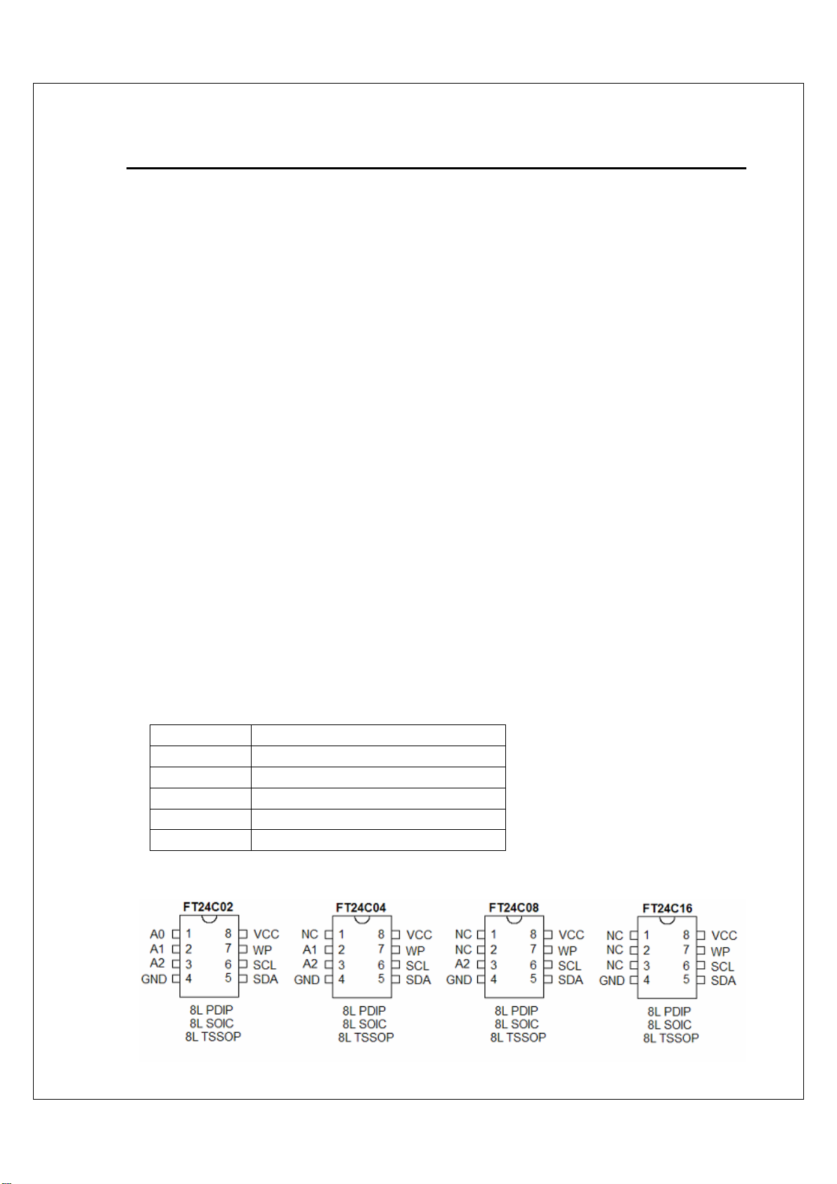
Fremont Micro Devices, Inc.
FEATURES
Low voltage and low power operati ons:
• FT24C02/04/08/16: V
• FT24C02A/04A/08A/16A: VCC = 1.8V to 5.5V
Maximum Standby current < 1µA (typically 0.02µA and 0.06µA @ 1.8V and 5.5V respectively).
16 bytes page write mode.
Partial page write operation allowed.
Internally organized: 256 × 8 (2K), 512 × 8 (4K), 1024 × 8 (8K), 2048 × 8 (16K).
Standard 2-wire bi-directional serial interface.
Schmitt trigger, filtered inputs for noise protection.
Self-timed programming cycle (5ms maximum).
Automatic erase before write operation.
Write protect pin for hardware data protection.
High reliability: typically 800,000 cycles endurance.
100 years data retention.
Industrial temperature range (-40o C to 85o C).
Standard 8-pin PDIP/SOIC/TSSOP Pb-free packages.
CC
FT24C02 / 04 / 08 / 16
FT24C02A / 04A / 08A / 16A
= 2.5V to 5.5V
and
DESCRIPTION
The FT24C02/04/08/16 series are 2048/4096/8192/16384 bits of serial Electrical Erasable and
Programmable Read Only Memory, commonly known as EEPROM. They are organized as
256/512/1024/2048 words of 8 bits (1 byte) each. The devices are fabricated with proprietary
advanced CMOS process for low power and low voltage applications. These devices are available in
standard 8-lead PDIP, 8-lead JEDEC SOIC and 8-lead TSSOP packages. A standard 2-wire serial
interface is used to address all read and write functions. Our extended V
devices enables wide spectrum of applications.
range (1.8V to 5.5V)
CC
PIN CONFIGURATION
Pin Name Pin Function
A2, A1, A0 Device Address Inputs
SDA Serial Data Input / Open Drain Output
SCL Serial Clock Input
WP Write Protect
NC No-Connect
All three packaging types come in conventional or Pb-free certified.
Page 16
HY5DU281622FT(P) Series
DESCRIPTION
The HY5DU281622FT(P) is a 134,217,728-bit CMOS Double Data R ate (D DR) Synchronous DRAM, ideally suited for the
main memory applications which requires large memory density and high bandwidth.
This Hynix 128Mb DDR SDRAMs offer fully synchronous operations referenced to both rising and falling edges of the
clock. While all addresses and control inputs are latched on the rising edges of the CK (fal ling edges of the /CK), Data,
Data strobes and Write data masks inputs are sampled on both rising and falling edges of it. The data paths are internally pipelined and 2-bit prefetched to achieve very high ban dwid th. All inp ut a nd output voltage levels are compatible
with SSTL_2.
FEATURES
•VDD, V
DDQ
= 2.3V
min
~ 2.7V
max
(Typical 2.5V Operation +/- 0.2V for DDR266, 333)
•VDD, V
DDQ
= 2.4V
min
~ 2.7V
max
(Typical 2.6V Operation +0.1/- 0.2V for DDR400
and 400Mbps/pin product)
• All inputs and outputs are compatible with SSTL_2
interface
• Fully differential clock inputs (CK, /CK) operation
• Double data rate interface
• Source synchronous - data transaction aligned to
bidirectional data strobe (DQS)
• x16 device has two bytewide data strobes (UDQS,
LDQS) per each x8 I/O
• Data outputs on DQS edges when read (edged DQ)
Data inputs on DQS centers when write (centered
DQ)
• On chip DLL align DQ and DQS transition with CK
transition
• DM mask write data-in at the both rising and falling
edges of the data strobe
• All addresses and control inputs except data, data
strobes and data masks latched on the rising edges
of the clock
• Programmable CAS latency 2/2.5 (DDR266, 333)
and 3 (DDR400 and 400Mbps/pin product) supported
• Programmable burst length 2/4/8 with both sequential and interleave mode
• Internal four bank operations with single pulsed
/RAS
• Auto refresh and self refresh supported
lock out function supported
RAS
•t
• 4096 refresh cycles/64ms
• JEDEC standard 400mil 66pin TSOP-II with 0.65mm
pin pitch
• Lead free (*ROHS Compliant)
ORDERING INFORMATION
Part No. Configuration Package
400mil
HY5DU281622F(L)TP-X* 8Mx16
* X means speed grade
** Lead-free product
*ROHS (Restriction Of Hazardous Substances)
Rev. 0.03 /Jun. 2006 3
66pin
TSOP-II**
OPERATING FREQUENCY
Grade Clock Rate Remark
-5 200MHz@CL3
-D43 200MHz@CL3 DDR400B (3-3-3)
-D4 200MHz@CL3 DDR400 (3-4-4)
- J 133MHz@CL2
- K 133MHz@CL2 133MHz@CL2.5 DDR266A (2-3-3)
- H 100MHz@CL2 133MHz@CL2.5 DDR266B (2.5-3-3)
166MHz @CL2.5
& @CL3
400Mbps/pin (maxi-
mum Date rate)
DDR333 (2.5-3-3)
DDR333 (3-3-3)
Page 17
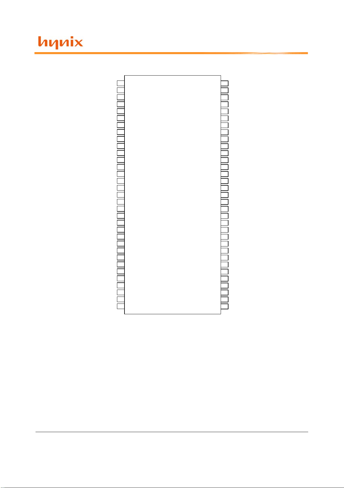
PIN CONFIGURATION
HY5DU281622FT(P) Series
V
DD
DQ0
V
DDQ
DQ1
DQ2
V
SSQ
DQ3
DQ4
V
DDQ
DQ5
DQ6
V
SSQ
DQ7
NC
V
DDQ
LDQ S
NC
V
DD
NC
LDM
/W E
/CAS
/RA S
/CS
NC
BA0
BA1
A10/AP
A0
A1
A2
A3
DD
V
10
11
12
13
14
15
16
17
18
19
20
21
22
23
24
25
26
27
28
29
30
31
32
33
1
2
3
4
5
6
7
8
9
400mil x 875m il
66pin TSOP-II
0.65mm pin pitch
66
65
64
63
62
61
60
59
58
57
56
55
54
53
52
51
50
49
48
47
46
45
44
43
42
41
40
39
38
37
36
35
34
V
SS
DQ15
V
SSQ
DQ14
DQ13
V
DDQ
DQ12
DQ11
V
SSQ
DQ10
DQ9
V
DDQ
DQ8
NC
V
SSQ
UDQS
NC
VREF
V
SS
UDM
/CK
CK
CKE
NC
NC
A11
A9
A8
A7
A6
A5
A4
SS
V
ROW AND COLUMN ADDRESS INFORMATION
• Organization : 2M x 16 x 4banks
• Row Address : A0 - A11
• Column Address : A0 - A8
• Bank Address : BA0, BA1
• Auto Precharge Flag : A10
• Refresh : 4K
Rev. 0.03 /Jun. 2006 4
Page 18
SHENZHEN TENA
ELECTRONICS CO., LTD.
PRODUCT
SPECIFICATION
MODEL
TNDT1A1200F
DESCRIPTION
DVB-T
PAGE
1
TNDT1A1200F
TNDT1A2200F
FOR DIGITAL TERRESTRIAL RECEPTION
A Original Release
REV DESCRIPTION DATE SIGN
CUSTOMER APPROVAL
DESCRIPTION
EUROPEAN DIGITAL
TERRESTRIAL STANDARD
DRAWING NO
REVISIONS
1.0
PAGES TOTAL
17
APPROVAL CHECK DESIGN
DATE DATE DATE
2008-10-16
Page 19
SHENZHEN TENA
ELECTRONICS CO., LTD.
PRODUCT
SPECIFICATION
MODEL
TNDT1A1200F
DESCRIPTION
DVB-T
PAGE
2
NO SPECIFICATION
1
FEATURES
1. +5V supply voltage only; no external tuning voltage required.
2. Tuners for horizontal and vertical mounting available.
3. Option with DC-power output through input connector (e. g. indoor antenna supply)
4. Tuners comply with relevant CENELEC standards with regard to requirements concerning signal
handling capability and immunity
5. Superior low noise and high sensitivity performance
6. RF-in to RF-out loopthrough amplifiers
7. low noise and excellent linearity
8. VHF high to UHF frequency range coverage
9. Standard connectors for in-and output e. g. IEC, F-connector. RCA
10. full UHF /VHF-H frequency coverage
11. Pattem generator included
2
12. I
C programmable
13. 400KHz Bus compliant
14. Stand-by mode addressable
15. High performance and cost effective single conversion tuner
2
16. I
C programmable
17. 400KHz Bus compliant
18. Fast PLL tuning speed (programmable step size e.g.62.5KHz and 166.67KHz)
19. Flat overall frequency response
20. High PLL loop bandwidth which ensures very low oscillator phase noise
21. SAW-filter and IF-amplifier included
a) Switchable 7/8 MHz SAW filter (full band tuners)
b) Fixed 8 MHz SAW filter (UHF only tuners)
c) IF-amplification controllable over a wide range
22. Differential, filtered (SAW)‘digital’ IF-output to directly drive the channel decoder
Page 20

Philips Semiconductors Product specification
Dual 4-channel analog multiplexer,
demultiplexer
FEATURES
• Wide analog input voltage range from −5 V to +5 V
• Low ON-resistance:
–80Ω (typical) at VCC− VEE= 4.5 V
–70Ω (typical) at VCC− VEE= 6.0 V
–60Ω (typical) at VCC− VEE= 9.0 V
• Logic level translation: to enable 5 V logic to
communicate with ±5 V analog signals
• Typical “break before make” built in
• Complies with JEDEC standard no. 7A
• ESD protection:
– HBM EIA/JESD22-A114-B exceeds 2000 V
– MM EIA/JESD22-A115-A exceeds 200 V.
• Specified from −40 °C to +85 °C and −40 °C to+125 °C.
APPLICATIONS
• Analog multiplexing and demultiplexing
• Digital multiplexing and demultiplexing
• Signal gating.
74HC4052; 74HCT4052
DESCRIPTION
The 74HC4052 and 74HCT4052 are high-speed Si-gate
CMOS devices and are pin compatible with the
HEF4052B. They are specified in compliance with JEDEC
standard no. 7A.
The 74HC4052 and 74HCT4052 are dual 4-channel
analog multiplexers or demultiplexerswith common select
logic. Each multiplexer has four independent
inputs/outputs (pins nY0 to nY3) and a common
input/output (pin nZ). The common channel select logics
include two digital select inputs (pins S0 and S1) and an
active LOW enable input (pin E). When pin E = LOW, one
of the four switches is selected (low-impedance ON-state)
with pins S0 and S1. When pin E = HIGH, all switches are
in the high-impedance OFF-state, independent of pins S0
and S1.
VCC and GND are the supply voltage pins for the digital
control inputs (pins S0, S1, and E). The VCC to GND
ranges are 2.0 V to 10.0 V for 74HC4052 and
4.5 V to 5.5 V for 74HCT4052. The analog inputs/outputs
(pins nY0 to nY3 and nZ) can swing between VCC as a
positive limit and VEE as a negative limit. VCC− VEE may
not exceed 10.0 V.
FUNCTION TABLE
ES1S0
L L L nY0 and nZ
L L H nY1 and nZ
L H L nY2 and nZ
L H H nY3 and nZ
H X X none
Note
1. H = HIGH voltage level
L = LOW voltage level
X = don’t care.
INPUT
For operation as a digital multiplexer/demultiplexer, VEEis
connected to GND (typically ground).
(1)
CHANNEL BETWEEN
Page 21

HIGHLY INTEGRATED LCD TV PROCESSOR
1. GENERAL DESCRIPTION
PPrreelliimmiinnaarry
SPV7100A
y
The SPV7100A is a highly integrated solution for the mainstream
LCD TV applications. The SPV7100A provides on-chip functions
including a high-speed triple-ADC and PLL, HDMI PanelLink
Cinema receiver, TV decoder with 3-D comb filter, 4-pair Audio
Line-In, 2-pair Audio Line-Out, one SIF demodulator and audio
decoder, 3D motion adaptive de-interlacing, 2:2/3:2 film mode
detection, video on graphic PIP/POP, SDRAM/DDR controller,
color management control, sRGB color management,
bitmap-based and font-based OSD engine, embedded CPU and a
dual channels LVDS transmitter. The chip could support LCD TV
up to 1080P input resolution and 1080p output resolution.
Note: PanelLink is the Trade Mark of Silicon Image Inc.
2. FEATURES
2.1. Graphics and Video Input Port
Integrate 150MHz 10-bit ADC/PLL
Dual CCIR656 digital video ports to support 2 input or 1 input/1
output
Support SDTV at 480i/576i and 480p/576p
Support HDTV at 720p and 1080i and1080p
Support PC graphics VGA, SVGA, XGA, WXGA, SXGA@75Hz
(135MHz)
Build-in sync. processor for separate, composite or sync on
Y/G
Support Video/Graphics PIP/DW
Channel swap for any source input
Image Format Detection/Auto Image Positioning/Auto Phase
Detection
Full SCART support including RGB fast blank
2.2. HDMI
HDMI 1.2 compliant and DVI 1.0 compliant receiver
HDCP 1.1 compliant receiver
Support DTV resolutions
(480i/576i/480p/576p/720p/1080i/1080p)
S/PDIF output supports PCM, Dolby Digital, DTS digital audio
with bypass mode
Four I2S audio outputs to SSD(Stereo Sound Decoder) with
bypass mode
Auto audio error detection with programmable soft mute
Build-in OTP for HDCP key
2.3. 3D Video Decoder
NTSC/PAL/SECAM video decoder
TM
3D comb filter for NTSC, PAL I (B,G,H,D,N), PAL-M, PAL-N
Enhanced NTSC/PAL/SECAM auto detection
4 analog inputs and one analog video output
Cross-color reduction for NTSC by 3-line comb filtering
Cross-color reduction for PAL by 5-line comb filtering
Motion adaptive 3D Y/C separation comb filter for NTSC/PAL
system
Multi-standard VBI data decoder, Teletext 2.5, WSS, VPS,
Closed-caption and V-chip
Macrovision detection
VBI data (C.C, TTX2.5, V-chip) overlay display
2.4. High Quality Video Processing
Enhanced Pixel-based 3D motion adaptive de-interlacing
(SDTV/HDTV)
Enhanced 2:2/3:2 film mode detection
Support Graphics mode frame rate conversion
Support Video mode frame rate conversion
2D Edge enhancement
Dynamic Peaking Filter
Enhanced Digital Luminance Transient Improvement (DLTI)
Digital Color Transient Improvement (DCTI)
Black/White Level Expansion and Dynamic Contrast
RGBYMC color adjustment
Dark and Gray area UV Suppression
Enhanced 3D motion adaptive noise reduction
De-blocking and de-mosquito filters
Color management/Color temperature adjustment
Brightness/Contrast/hue/Saturation adjustment
Support sRGB color correction
Build-in three 256-point gamma tables with 10 bits resolution
Color space conversion, both YCbCr to RGB and RGB to
YCbCr
Build-in temporal/spatial color dithering
10-bit video/image processing
2.5. High Quality Video Scaling Engine
Advanced third-generation scaling engine
Support 4:3 / 16:9 with non-linear scaling
Support Moiré Canceling
Page 22

2.6. Multi-standard TV Sound Decoder
Field proven TV sound decoder
Support BTSC, A2/Zweiton, NICAM, EIAJ, SECAM, FM stereo
Automatic TV-standard detection (ASD)
Non-standard carrier compatible
SAP decoding where applicable
Auto fallback from NICAM where applicable
2.7. Embedded OSD and VBI Controller
Build-in programmable OSD engine for two OSD windows (bit
map OSD)
1,2,4 and 8-bit per pixel (bit-map OSD)
Support hardware cursor
Support programmable 512 font-based OSD and
graphics-based OSD
Support VBI decoder (CC,V-Chip and Teletext)
Support VBI CC/TTX/Menu with more than 1000 char-fonts
2.8. Embedded DDR/SDRAM Controller
Integrated DDR/SDRAM controller with DLL (DDR)
Support 32-bit DRAM bus with memory size from 16Mb (limited
functions) to 256Mb
2.9. Programmable Digital Output for LCD
Support output sequence mapping for TI and Thine
Build-in dual channels 8-bit LVDS Tx or single channel 10-bit
LVD S Tx
Support display output up to 1920x1200 @60Hz (165Mhz
WUXGA reduced blanking)
Support Power Down Sequence
4-ch PWM backlight intensity control
2.10. CPU
Powerful 32-bit RISC CPU
Simple memory management stub (SMMU)
MIPS-I instruction with DSP instruction set extension
2K bytes 2-way instruction cache
4K bytes direct-mapped data cache
8K bytes data memory for DMA operation
EJTAG interface
One UART up to 115200 baud rate
Four 24-bit up/down timers
3K Bytes IMem for power saving mode
2.11. Audio Processor
Support SPDIF input
Support SPDIF output (signal could come from SPDIF input or
SSD)
Support up to 8 channels I2S I/O
4 channels audio DAC output
4 channels audio ADC input
Channel: L, R, C, S, Sub, Aux1, 2 and 3 @ 32 kHz
5- band Equalizer
3-D surround sound
Bass management
Volume control
Support sub-woofer output
Sample rate conversion
SSD could output up to 3 sources
Virtual Dolby Surround (VDSII 422 and 423) (support by
SPV7100AxD)
SRS TruSurround (XT, WOW, 3D Sound) (support by SPV7100
AxS)
2.12. Misc
Build-in TV remote control 1 infra-red receiver interface
2-channels 6-bits ADC for key scan function
Build-in pattern generator for auto testing
256-pin LQFP for LCD application
PPrreelliimmiinnaarry
SPV7100A
y
© Sunplus Technology Co., Ltd.
Proprietary & Confidential
5 MAR. 23, 2007
Preliminary Version: 0.1
Page 23

4.3. List of Packages and Pins
4.3. List of Packages and Pins
4.3.1. 256- LQFP Package
4.3.1. 256- LQFP Package
SPV7100A
SPV7100A
Figure 4-1 SPV7100A Pin Configuration
Figure 4-1 SPV7100A Pin Configuration
Page 24

V1.5
Desktop DVD Player SOC
PRELIMINARY, SUBJECT TO CHANGE WITHOUT NOTICE MTK CONFIDENTIAL, NO DISCLOSURE
MT1389L
5 Function
5-1 General Description
MediaTek MT1389L is a cost-effective DVD system-on-chip (SOC) which incorporates advanced features like
MPEG-4 video decoder, high quality TV encoder and state-of-art de-interlace processing. The MT1389L enables
consumer electronics manufacturers to build high quality, USB2.0, MS/SD/MMC reader, feature-rich DVD players,
portable DVD players or any other home entertainment audio/video devices.
World-Leading Technology: Based on MediaTek’s world-leading DVD player SOC architecture, the
MT1389L is the New generation of the DVD player SOC. It integrates the MediaTek 3
RF amplifier and the Servo/MPEG AV decoder.
Rich Feature for High Valued Product: To enrich the feature of DVD player, the MT1389 equips a
simplified MPEG-4 advanced simple profile (ASP) video decoder to fully support the DivX
makes the MT1389-based DVD player be capable of playback MPEG-4 content which become more and more
popular.
Incredible Audio/Video Quality: The progressive scan of the MT1389L utilized advanced motion-adaptive
de-interlace algorithm to achieve the best movie/video playback. It also supports a 3:2 pull down algorithm to give
the best film effect. The 108MHz/12-bit video DAC provides users a whole new viewing experience. Built-in 6ch
audio DACs and 2ch audio ADCs could give the variable function solutions.
High Performance Memory Storage Device: As the core of Portable DVD players need more capability to
support current multimedia contents. The MT1389L provides the interface for the 3-in-1 card reader, which
supports Memory-Stick, Secure Digital Memory Card, and MultiMediaCard, to connect with the mainstream digital
camera FLASH cards. For the USB application, we adopt USB2.0 High speed specification to reach rich-contents
transference. USB 2.0 High speed will support for high-speed devices. USB 2.0 High Speed is suitable for
high-performance devices such as high-density storage devices. In addition, USB 2.0 High Speed supports old
USB 1.0/1.1 software and peripherals, offering impressive and even better compatibility to customers
rd
generation front-end digital
1
Home Theater profile. It
Key Features
DVD
PUH
Module
FLASH
MT1389L
Desktop
CVBS, Y/C,
Component
SDPIF
Analog
Audio
Output
USB 2.0
High Speed
Front-panel
Remote
DRAM
DVD Player System Diagram Using MT1389L
1
DivX is a trademark of DivXNetworks
2
USB High Speed : 480Mbit/sec. USB Full Speed : 12Mbit/sec.
All information contained herein is the exclusive property of MediaTek Inc. and shall not be distributed, reproduced
or disclosed in whole or in part without prior written permission of MediaTek Inc
4
RF/Servo/MPEG Integration
DivX Home Theater Level MPEG4 ASP Video decoder
Support Nero-Digital
Support DivX Ultra
High Performance Audio Processor
Progressive Scan
108MHz/12-bit, 4 CH TV Encoder
Internal 6CH Audio DAC
Internal 2CH Audio ADC
USB2.0 High Speed (Host/Device)
3-in-1 MS/SD/MMC reader
Applications
Standard DVD Players
Page 25

V1.5
GPIO13
AudioAudioVid
DAC
ADC
DAC
_
DVDD18
INT RF
GPIO9
XTAL I
GPIO8
XTALO
GPIO7 / CKE
V20
V14
REXT
USB
DVSS18
_
_
MT1389L
Desktop DVD Player SOC
PRELIMINARY, SUBJECT TO CHANGE WITHOUT NOTICE MTK CONFIDENTIAL, NO DISCLOSURE
6 Pin Assignment
AKIN1 / GPIO21 / Audio_mute
AKIN2 / GPIO19 / Audio_mute
ALF / CENTER / GPIO
RFH / OPINN /
RFIN / OPOUT /
RFG / OPINP /
128
127
126
1 96 VREF
RFA
2 95 DACVDDC
RFB
3 94
RFC
4
RFD
5
RFE
6 91 GPIO10
RFF
7 90
2
AVDD18
AVDD33_1
AGND33
AVDD33_2
TRAY
TRAY
FG / GPIO2 26 71 R A7
USB_DP 27 70 R A8
USB_DM 28 69 RA9
VDD33_USB 29 68 DVDD33
VSS33_USB 30 67 RA11
PAD_VRT 31 66 RCLK
VDD18_USB 32 65 DQM1
8
9 88
10 87
11 86 RA3
12 85 RA2
13 84 DVDD33
14 83 RA1
15 82 RA0
MDI1
16 81 RA10
MDI2
17 80 BA1
LDO1
18
LDO2
19 78 BA0
20 77 RAS#
DMO
21 76 CAS#
FMO
22 75 RW E#
OPEN
23 74 RA4
CLOSE
24 73 RA5
TRO
25 72 RA6
FOO
33343536373839404142434445464748495051525354555657585960616263
GPIO3 / INT#
GPIO4
GPIO6
RFIP
125
SF_CS_
AVDD18_1
AGND18
124
123
SF_DO
SF_DI
ADACVDD2
ADACVDD1
122
121
SF_CK
UP1_6 / SCL
120
UP1_7 / SDA
ALS / GPIO
119
ICE
AL / GPIO1
118
PRST#IRRD0
ARF / LFE / GPIO
ARS / GPIO
ADACVSS1
115
114
ADACVSS2
113
112
APLLCAP
111
AR / GPIO0
AVCM
117
116
MT1389L
Desktop
RD1
RD2
RD3
RD4
DVDD33
APLLVDD
110
RD5
AADVDD
109
RD6
108
RD7
ADVCM / GPIO20 /
107
DVDD18
106
DQM0
AADVSS
R
105
104
RD15
RD14
B
103
RD13
G
102
RD12
eo
DACVDDA
101
DVSS33
DACVDDB
100
RD11
DACVSSC
CVBS
FS
999897
93 SPDIF / GPIO12
92 GPIO11
89
79
64
RD10
RD9
RD8
All information contained herein is the exclusive property of MediaTek Inc. and shall not be distributed, reproduced
20
or disclosed in whole or in part without prior written permission of MediaTek Inc
Page 26

EN25B16
EN25B16
16 Mbit Serial Flash Memory with Boot and Parameter Sectors
FEATURES
x Single power supply operation
- Full voltage range: 2.7-3.6 volt
x 16 M-bit Serial Flash
- 16 M-bit/2048 K-byte/8192 pages
- 256 bytes per programmable page
x High performance
- 75MHz clock rate
x Low power consumption
- 5 mA typical active current
- 1 PA typical power down current
x Flexible Sector Architecture:
- Two 4-Kbyte, one 8-Kbyte, one 16-Kbyte,one
32-Kbyte, and thirty one 64-Kbyte sectors
x Software and Hardware Write Protection:
- Write Protect all or portion of memory via
software
- Enable/Disable protection with WP# pin
x High performance program/erase speed
- Byte program time: 7μs typical
- Page program time: 1.5ms typical
- Sector erase time: 300 to 800ms typical
- Chip erase time: 18 Seconds typical
x Minimum 100K endurance cycle
x Package Options
- 8 pins SOP 200mil body width
- 8 contact VDFN
- 16 pin SOP 300mil body width
- All Pb-free packages are RoHS compliant
x Commercial and industrial temperature
Range
GENERAL DESCRIPTION
The EN25B16 is a 16M-bit (2048K-byte) Serial Flash memory, with advanced write protection
mechanisms, accessed by a high speed SPI-compatible bus. The memory can be programmed 1 to
256 bytes at a time, using the Page Program instruction.
The EN25B16 has thirty six sectors including thirty one sectors of 64KB, one sector of 32KB, one sector
of 16KB, one sector of 8KB and two sectors of 4KB. This device is designed to allow either single Sector
at a time or full chip erase operation. The EN25B16 can protect boot code stored in the small sectors for
either bottom or top boot configurations. The device can sustain a minimum of 100K program/erase cycles
on each sector.
This Data Sheet may be revised by subsequent versions ©2004 Eon Silicon Solution, Inc., www.essi.com.tw
or modifications due to changes in technical specifications.
Rev. C, Issue Date: 2006/12/22
1
Page 27

Figure.1 CONNECTION DIAGRAMS
ʳ
EN25B16
8 - LEAD SOP
8 - CONTACT VDFN
16 - LEAD SOP
This Data Sheet may be revised by subsequent versions ©2004 Eon Silicon Solution, Inc., www.essi.com.tw
or modifications due to changes in technical specifications.
Rev. C, Issue Date: 2006/12/22
2
Page 28

Figure 2. BLOCK DIAGRAM
EN25B16
This Data Sheet may be revised by subsequent versions ©2004 Eon Silicon Solution, Inc., www.essi.com.tw
or modifications due to changes in technical specifications.
Rev. C, Issue Date: 2006/12/22
3
Page 29

SDRAM 64Mb H-die (x4, x8, x16)
CMOS SDRAM
4M x 4Bit x 4 / 2M x 8Bit x 4 / 1M x 16Bit x 4 Banks SDRAM
FEATURES
• JEDEC standard 3.3V power supply
• LVTTL compatible with multiplexed address
• Four banks operation
• MRS cycle with address key programs
-. CAS latency (2 & 3)
-. Burst length (1, 2, 4, 8 & Full page)
-. Burst type (Sequential & Interleave)
• All inputs are sampled at the positive going edge of the system clock
• Burst read single-bit write operation
• DQM (x4,x8) & L(U)DQM (x16) for masking
• Auto & self refresh
• 64ms refresh period (4K cycle)
GENERAL DESCRIPTION
The K4S640432H / K4S640832H / K4S641632H is 67,108,864 bits synchronous high data rate Dynamic RAM organized as 4 x
4,194,304 words by 4 bits, / 4 x 2,097,152 words by 8 bits, / 4 x 1,048,576 words by 16 bits, fabricated with SAMSUNGcs high performance CMOS technology. Synchronous design allows precise cycle control with the use of system clock I/O transactions are possible
on every clock cycle. Range of operating frequencies, programmable burst length and programmable latencies allow the same device to
be useful for a variety of high bandwidth, high performance memory system applications.
Ordering Information
Part No. Orgainization Max Freq. Interface Package
K4S640432H-TC(L)75 16Mb x 4 133MHz(CL=3)
K4S640832H-TC(L)75 8Mb x 8 133MHz(CL=3)
K4S641632H-TC(L)60
K4S641632H-TC(L)70 143MHz(CL=3)
K4S641632H-TC(L)75 133MHz(CL=3)
Organization Row Address Column Address
4Mb x 16
16Mx4 A0~A11 A0-A9
8Mx8 A0~A11 A0-A8
4Mx16 A0~A11 A0-A7
Row & Column address configuration
166MHz(CL=3)
LVTTL 54pin TSOP(II)
Rev. 1.5 February 2004
Page 30

SDRAM 64Mb H-die (x4, x8, x16)
Package Physical Dimension
CMOS SDRAM
0.10
0.004
MAX
#54
#1
0.71
( )
0.028
#28
11. 76r0.20
0.463r0.008
#27
22.62
MAX
0.891
22.22
0.30
0.012
0.875
+0.10
-0.05
0.004
-0.002
r0.10
r0.004
0.80
0.0315
0.21
0.008
r0.05
r0.002
0.039
54Pin TSOP(II) Package Dimension
1.00
r0.10
r0.004
0.25
0.010
10.16
0.125
0.005
0.047
0.400
1.20
TYP
+0.075
-0.035
+0.003
-0.001
MAX
0.05
0.002
0~8qC
0.45~0.75
0.50
MIN
0.018~0.030
)
0.020
(
Rev. 1.5 February 2004
Page 31

SDRAM 64Mb H-die (x4, x8, x16)
FUNCTIONAL BLOCK DIAGRAM
Bank Select
CMOS SDRAM
LWE
Data Input Register
LDQM
CLK
ADD
Refresh Counter
Row Buffer
Address Register
LRAS
LCBR
LCKE
LRAS LCBR LWE LDQM
CLK CKE CS
Samsung Electronics reserves the right to change products or specification without notice.
*
Row Decoder Col. Buffer
LCAS LWCBR
Timing Register
RAS CAS WE L(U)DQM
4M x 4 / 2M x 8 / 1M x 16
4M x 4 / 2M x 8 / 1M x 16
4M x 4 / 2M x 8 / 1M x 16
4M x 4 / 2M x 8 / 1M x 16
Column Decoder
Latency & Burst Length
Programming Register
Sense AMP
Output BufferI/O Control
DQi
Rev. 1.5 February 2004
Page 32

5
+12V_IN
+12V_IN
R446
1k
C352
1uF
D60
BAV99
E1
+
47uF
R459
47K
GND_PHONE
R464
47K
GND_PHONE
GND_AMP
GND_AMP
R442
nc
R450
470K
R454
470K
EC80
+
2.2uF
R457
100K
R460 10K
C359
820pF
R462
100K
R466 10K
C362
820pF
+12V_IN
12
1 2
PVCC6
PVCC6
R379
NC
GND_AMP
1
GND_PHONE
2
3
PVCC12
GND_PHONE
6
5
PVCC12
R443
47k
1 2
1 2
Q60
2N3904
+
32
Q63
2N3906
C357
100pF
-
+
8 4
C360
100pF
-
+
8 4
R445
47k
EC88
47uF16V
GND_AMP
1
U6A
NJM4558
7
U6B
NJM4558
R455
22K
R451
470
Q59
2N3904
1 2
GND_AMP
C364
10uF
C365
10uF
HPD_PHONE
R384
6.8K
+12V_IN
+12V_IN1,5,10
GND1,2,3,4,5,6,7,8,9,10,12,13,14,15
AOUT1R
AOUT1R7
AOUT1L
AOUT1L7
MUTE_AMP
D D
C C
B B
MUTE_AMP7
MUTE_AMP
+12V_IN
GND_PHONE
1 2
3
2
R456
100K
C358
1uF
C361
1uF
1
GND_AMP
MUTE_AMP7
AOUT1L
AOUT1R
4
R447
100K
R467
8.2K
Q62
2N3904
PHONE OUT
GND_PHONE
R461
10R
PHONE_OUTR
PHONE_OUTL
R268
10R
R283
75R
R444
22K
MUTE_C
C371
EC87
+
10uF
47uF16V
Q61
2N3904
C350
GND_AMP
1uF
GND_AMP
MUTE_C
R498
220
R282
R458
1K
1K
PVCC12 PVCC6
R465
C366
10uF
GND_PHONE
HPD_PHONE
20K
CON9
PHONE
1
2
3
4
5
R284
20K
R463
100K
3
SPEAKER OUT
SPEAKER_ROUT
SPEAKER_LOUT
GND_AMP
R440
NC/8.2K
R441 0
AOUT1_LAOUT1L
RIN
LIN
EC83
MUTE_C
GND
GND
EC76
220uF/16V
GND
EC78
220uF/16V
A_POWER
AOUT1_RAOUT1R
R448 0
R449
NC/8.2K
GND_AMP
R4522.2
R4532.2
C353
0.1uF
C356
C355
0.1uF
0.1uF
R269
47K
SPEAKER OUT
+12V_IN
SPEAKER_LOUT
+12V_IN
U26
PWR GND
PRE GND
Ripple Filter
LA42102
+OUT1
-OUT1
-OUT2
+OUT2
MUTE
Stanby
C368
0.1uF
NC
VCC
IN2
IN1
L43
22uH/2A
470uF/16V
GND_AMP
13
12
11
10
9
8
7
6
5
4
3
2
1
47UF/16V
SPEAKER_ROUT
EC79
A_POWER
MUTE_C
EC82
GND_AMP
R2652.2
R2662.2
47UF/16V
+12V_IN
GND_PHONE
AOUT1R
AOUT1L
MUTE_AMP
C367
10uF
+12V_IN
+12V_IN1,4,9
GND1,2,3,4,5,6,7,8,9,10
AOUT1R6
AOUT1L6
MUTE_AMP6
C351
2.2uF
C354
0.1uF
+12V_IN
GND_AMP
C363
2.2uF
2
LIN
EC75
100uF/16V
RIN
GND_AMP
U27
1
-INV1
2
SGND
3
SVRR
4
OUT1
5
PGND
6
OUT2
7
VP
8
M/SS
9
-INV2
GND10GND
J15
1
2
3
4
DIP/PIN4/2.0
TDA1517P
1
J14
1
2
3
4
DIP/PIN4/2.0
21
20
sink
GND
19
GND
18
GND
17
GND
16
GND
15
GND
14
GND
13
GND
12
GND
11
sink
22
GND_AMP
GND_PHONE GND_AMP
A A
5
4
3
2
1
Page 33

5
4
3
2
1
CON6
NC_4PIN/2.0mm
1
2
3
4
F1
CN3
DC-JACK-2mm
D D
C C
+5VSB
C19
0.1uF
+5VSB
+3V3_SW7100
B B
+12V_power
1
2
3
10
9
8
7
6
5
4
3
2
1
CN2
CON10/2.54mm
+5V_DC +5VSB
L19
0R
STANDBY
UP2
4
ADJ/GND
AP1117-25/SOT-223
SOT-223
C7
0.1uF
4
4
C77
UP4
0.1uF
1117-ADJ
SOT-223
OUT
IN
IN
OUT
ADJ
+12V_IN
5A/12V
+5VSB GND
STB_CON
POWER_ON
3
2
1
UP3
3
IN
AP1084-3V3/256
TOP-263
2
OUT
+3.3V Regulator
1
ADJ
3
2
1
10/26 Add
+5VSB1
R143
220R
R138
100R
L5
22uH/3A/DIP
1 2
EC50
470uF/25V
100K
+2V5
+
+3V3
+
+1V8_ADCA
EC34
+
100uF/16V
10K
R58
R42
EC12
100uF/16V
EC33
100uF/16V
EC37
470uF/25V
+5V_DC
+5VSB
+12V_IN
2
Q12
2N3904
Q15
AP2301
SOT-23
3 1
R437
NC
R438
0ohm-0805
C220
0.1uF
470uF/25V
+5V_SW
L42
22uH/2A
1 2
EC62
C369
10uF
470uF/25V
C221
0.47uF
EC63
U21
OCP2030SA
1
VCC
2
SCP
C2
0.1uF
11/30 Modify
R320
1K
IR
L20
1 2
22uH/4A(33uH/4A)
D33
B340B
R123
100K
+5VSB1
R503 nc
AX3101
OUTPUT
OUTPUT
VSS
8
C218
C217
0.1uF
1uF
+3V3
2
R127
10K
Q24
2N3904
R499
nc
R501
nc
5
6
1
8
LX
7
LX
3
IN
FB4GND5GND
6
C222
2200pF
STANDBY
POWER_ON
R6
1K3
FOR SPV7100 ONLY 3.3V 1.8V 2.5V
U1
4
VCC
OCSET3EN2VSS7FB
R7
100K
C4
0.1uF
3 1
XT4
nc
CRISTAL-B
PICVPP
D3
SK34/SOP
SR34B
EC52
470uF/16V
Q23
AP2301
2
L2 22uH/2A
R318
9K1
R494
1K
R488
100
C385
0.1uF
R319
1K1%
+3V3_SW
C370
10uF
Q64
AP2301
3 1
U28
1
VDD
2
GP5/T1CKI/OSC1/CLKIN
3
GP4/AN3/T1G/OSC2/CLKOUT
4
GP3/MCLR/VPP
PIC12F675
R439
2K2
R41
390
R33
2K
5.6V
+5V_DC
R486
nc
R487
nc
GP0/AN0/CIN+/ICSPDAT
GP1/AN1/CIN-/VREF/ICSPCLK
GP2/AN2/T0CKI/INT/COUT
+1V8
C1
1000pF
EC21
C37
470uF/16V
0.1uF
D41
1 2
+3V3_SW7100
+
+12V_IN
+5V_SW
+5VSB
STB_AC_ON7
POWER_ON7
+3V3
+1V8
VSS
+12V_IN
+5V_SW
+5VSB
+3V3
+1V8
8
7
6
5
+5VSB
R227
10K
STB_CON
3
Q30
2
1
2N3904
SOT-23
STB_AC_ON
POWER_ON
+12V_IN5,10,11
+5V_SW 3,4,12,13,15
+5VSB 5,9,10,13
+3V3 2,3,7,8,9,10,13,14,15
+1V8 8
GND 2,3,4,5,6,7,8,9,10,11,12,13,14,15
R500
C393
nc
nc
GND
GND
R504 nc
R506 nc
R228 4.7K
OFF
KPD_POWER
MCU_IO
GND_PWRGND_TMDSGNDV
STB_AC_ON
PICVPP
PICPGD
PICPGC
R505 nc
ON
CN11
HEADER5-2.54
5
4
3
2
1
STB_CON
A A
Title
Size Document Number
C
5
4
3
2
Date: Sheet of
SUNPLUS
System Power
SPTV05-13-V1
1
Rev
1.0
1 15Sunday, June 15, 2008
Page 34

5
HDMI Input
Layout Note
differential impedance 100ohm
CN4
20
SHELL1
D D
GND_CASE
C C
SHELL221D2+
22
SHELL3
23
SHELL4
HDMI CON-SMT
D2 Shield
D1+
D1 Shield
D0+
D0 Shield
CK+
CK Shield
CE Remote
DDC CLK
DDC DATA
GND
+5V
HPD
D2-
D1-
D0-
CK-
1
2
3
4
5
6
7
8
9
10
11
12
13
14
NC
15
16
17
18
19
GND_TMDS
EDID Defult: NOT write protect
10K
R160
4.7K
NC/10K
5v_hdmi
R158
/WP
R323
GND_TMDS
RXP2
RXM2
RXP1
RXM1
RXP0
RXM0
RXCP
RXCM
ASCL
ASDA
+5V_HDMI_A
R298
nc
5v_hdmi
R159
4.7K
5v_hdmi
D6
3
4
INPUT1
BAT54C
2
+5V_DC
1
+5V_HDMI_A
U1424C02
8
VCC
7
WP
6
SCK
5
SDA
C105 1uF
VSS
A0
A1
A2
1
2
3
4
GND_TMDS
3
RXP2 RXM2 RXP1 RXM1
DM8
NC
GND_TMDS GND_TMDS GND_TMDS GND_TMDS
RXP0 RXM0 RXCP RXCM
DM6
NC
GND_TMDS GND_TMDS GND_TMDS GND_TMDS
ASCL
DM4
NC
DM2
NC
R324 33
DM7
NC
DM5
NC
ASCL
DM3
NC
DM1
NC
SCL_HDMI 7
GND_TMDS
ASDA
GND_TMDS
DM10
NC
DM9
NC
RXP0
RXM0
RXP1
RXM1
RXP2
RXM2
RXCP
RXCM
SOG_IN
B_IN
G_IN
R_IN
2
ISP_TRAP
RXP0 7
RXM0 7
RXP1 7
RXM1 7
RXP2 7
RXM2 7
RXCP 7
RXCM 7
+5V_DC
SOG_IN 3,7
B_IN 7
G_IN 7
R_IN 7
R105 10K
R313
100K
+3V3
2
SCL_VGA
SDA_VGA
VS_VGA
HS_VGA
HPD_PC
/WP
+5V_DC
+3V3
HOLD_FLASH
3
Q22
2N3904
1
SCL_VGA 7
SDA_VGA 7
VS_VGA 7
HS_VGA 7
HPD_PC 7
/WP 7
+3V3
WP# 9
10/25 Modify
R114
100K
1
+5V_DC1,3,9,10,13
+3V31,3,7,8,9,10,13,14,15
GND1,3,4,5,6,7,8,9,10,11,12,13,14,15
HOLD_FLASH7
R297
2
GND_TMDS
1K
3
Q35
Si2302
1
VGA Analog Input
SCL_VGA2
SDA_VGA2
D11
D27
nc
1 2
1 2
GND_ADC
GND_ADC
R327 NC/33
R328 33
+5V_VGA
nc
GND_ADC
GND_ADC
4
15
10
14
13
12
9
8
7
6
CN5
VGA/CON
5
4
3
2
111
VGA Con.
DSUB 15Pin-3/Female
16
17
D13
5.6V
1 2
GND_CASE GND_TMDS GND_TMDSGND_ADCGND_CASE
R326 nc
R296
1K
3
R136
HPD_HDMI7
B B
A A
HPD_HDMI
GND_ADC
VS_VGA
R208 100
HS_VGA
R199 100
C149
C150
NC
GND_ADC GND_ADC
NC
5
1K
Q34
Si2302
2
1
R206
R207
510
510
ASDA
GND_ADC
GND_ADC
+5V_DC +5V_DC +5V_DC
1
2
D31
D30
BAV99L
BAV99L
3
VGA_BIN
VGA_GIN
VGA_RIN
D12
5.6V
1 2
GND_ADC
GND_ADC
1
2
D32
BAV99L
3
R263
R264 22R
R325 33
R311 10K
R309 NC
1
2
3
22R
3
1 2
GND_ADC
PC-BIN
C212
NC/22pF
ISP_TRAP
HPD_PC
D28
nc
PC-GIN
PC-RIN
C213
NC/22pF
GND_ADC
TXD 7,9
RXD 7,9
SDA_HDMI 7
C214
NC/22pF
PC-BIN
PC-GIN
PC-GIN
R300
R301
75R
75R
GND_ADC
PC DDC
D29
3
BAT54C
C184
1uF
GND_ADC GND_ADC
R209 100R
R210 100R
PC-RIN R_IN
PC-RIN
2
1
2
R302
75R
+5V_DC
+5V_VGA
+5V_DDC
U19
A01VCC
A12WP
A23SCL
GND4SDA
24C02
DDC EDID Data
SOP 8Pin
R211 100R
+5V_DDC
8
7
6
5
GND_ADC
SCL_VGA2
SDA_VGA2
ISP FROM VGA
GND_ADCGND_ADC
B_INPC-BIN
C151
0.01uF
G_IN
C152
0.01uF
C153
0.01uF
+5V_DDC
R254
R251
2K2
2K2
R252 100
R253 100
Title
Size Document Number
Date: Sheet of
HDMI Switch
Custom
SCL_VGA
SDA_VGA
SUNPLUS
SPTV05-13-V1
1
Rev
1.0
2 15Thursday, June 12, 2008
Page 35

5
+5V_SW
+5V_SW1,4,12,13,15
CN7
SHILED
VOUT
GNDVI
GNDVO
RGBSW
RIN
GNDSW
GNDR
GIN
GNDG
FunSel
BIN
GNDB
AOL
AOR
SCART Connector
CN9
7
Y
7
8
8
Pb
9
9
Pr
10
10
11
11
12
12
13
13
Y
14
14
Pb
15
15
16
Pr
16
AV1-3X2
GND
TXD_1003
RXD_1003
VIN
N.C.
N.C.
AIL
GNDA
AIR
1
3
5
2
4
6
21
20
19
18
17
16
15
14
13
12
11
10
9
8
7
6
5
4
3
2
1
L29
120ohm/100MHz
L30
120ohm/100MHz
L31
120ohm/100MHz
,4,5,6,7,8,9,10,11,12,13,14,15
D D
Y Pr Pr CVBS
C C
B B
+5V_SW
TXD_1003 2,7,9
RXD_1003 2,7,9
5.6V
SC1_FB
SC1_RIN
SCART_ISP
SC1_GIN
SC1_FS
SC1_BIN
SC1_AU_LIN
SC1_AU_LOUT
SC1_AU_RIN
SC1_AU_ROUT
GNDV
AV_VIN
SC2_AU_LIN
SC2_AU_RIN
3
3
BAV99L
BAV99L
BAV99L
D22
D23
D21
1
2
1
2
2
+5V_DC
GND_ADCGND_ADC
+5V_DC
GND_ADC +5V_DC
D25
GNDV
R286NC/0R
R287NC/0R
3
GND_ADC
1
1 2
av_1_out
R-0603
R-0603
R304
75R
12
12
C199
220pF
RXD_1003
TXD_1003
R274
75R
L14
1.8uH
DTV_Y_IN1
DTV_Pb_IN1
DTV_Pr_IN1
R270
75R
DVD_Y_IN13
DVD_PB_IN13
DVD_PR_IN13
CVBS2_INav_1_in
C185
220pF
av_1_out 3
R289
10K
D17
nc/15V
1 2
SC1_AU_LOUT SC1_AU_ROUT
4
11/28 Modify
CVBS2_IN 7
R258
75R
GNDV
R216
2.4K
1 2
GNDVGNDV
D18
9.2V
1 2
SCART1 AV+RGB
FS -> SOY2 / SARIN1
0-2v: TV Mode -> 0-0.4v
5-8v: 16:9 AV -> 1.0-1.6v
9.5-12v: 4:3 AV -> 1.9-2.4v
SOG_IN
SOY2_IN
D24
R303
5.6V
75R
GNDVGNDV
D19
9.2V
1 2
SC1_BIN
BAV99L
D16
SC1_GIN
BAV99L
D15
SC1_RIN
SOG_IN 7
SOY2_IN 7
SC1_AU_LOUT
SC1_AU_ROUT AOUT0R
SC1_AU_RIN
AU_AIN1L
AU_AIN1R
AV_VIN
DTV_Y_IN1
DTV_Pb_IN1
DTV_Pr_IN1
GNDV
C3271uF
C3281uF
R190 10K
R312 10K
AU_AIN1L 4
AU_AIN1R 4
D20
1 2
GNDV
C238
R330 22K
BAV99L
R292
47K
C215
220pF
5.6V
+5V_SW_4052
R329
22K
10uF
GNDV
PI5V330
R230
D14
R412
10R
2
47K
R314
6.8K
2
5
11
14
3
6
10
13
2
2
3
L17
1.8uH
3
1
+5V_DCGND_ADC
3
1
+5V_DCGND_ADC
1
+5V_DCGND_ADC
AOUT0L
16
U18
1A
1B
1C
1D
2A
2B
2C
2D
8
3
C232
220pF
GNDV GNDV
C234
220pF
GNDV GNDV
C236
220pF
GNDV GNDV
AU_AIN1LSC1_AU_LIN
AU_AIN1R
R186
6.8K
C207
220pF
GNDV
C223
1uF
GNDV
4
A
7
B
VCC
9
C
12
D
15
EN
1
S
VSS
L21
1.8uH
L22
1.8uH
L23
1.8uH
GNDV
CVBS0_IN
R259
75R
C233
220pF
C235
220pF
C237
220pF
GNDV
AOUT0L
AOUT0L7
AOUT0R
AOUT0R7
11/28 Modify
CVBS0_IN 7
SW_HD
R244
R245
75R
75R
SW_HD 7
R242
75R
SCART_ISP
SC2_AU_LIN
C324
2.2uF
C-0603
C325
2.2uF
C-0603
C326
2.2uF
C-0603
R243
100R
R213
0R
R246
100R
R257
100R
GND_ADC
PR2_IN
PB2_IN
Y2_IN
C155
NC/10pF
R12810K
11/28 Modify
PR2_IN 7
PB2_IN 7
Y2_IN 7
2
R306 10K
R308 10K
C158
0.01uF
C131
1000pF
C165
0.01uF
C179
0.01uF
2
+3V3
R129
NC/100K
SCART_ISP_TRAP
3
Q21
2N3904
1
R104
100R
ISP FROM SCART
GND
R307
6.8K
Y1_IN
SOY1_IN
PB1_IN
PR1_IN
AU_AIN2L
AU_AIN2RSC2_AU_RIN
R305
6.8K
Y1_IN 7
SOY1_IN 7
PB1_IN 7
PR1_IN 7
SCART_ISP_TRAP13
AU_AIN2L
AU_AIN2R
AU_AIN2L 4
AU_AIN2R 4
11/28 Modify
1
11/30 Modify
GND_ADC
GNDV
A A
Title
Size Document Number
C
5
4
3
2
Date: Sheet of
SUNPLUS
Input-2 Video
SPTV05-13-V1
1
Rev
1.0
3 15Thursday, May 01, 2008
Page 36

5
PC Audio Input
CN6
D D
C C
PHONE
Stereo Audio In
2
5
1
3
R-Pho L-Pho
L-Out
Stereo Audio Connector
Top Diagram
DVB_AL_OUT13
DVB_AR_OUT13
AIN2L
AIN2R
AIN3L
AIN3R
AU_SW0
AU_SW1
AU_AIN1L
AU_AIN1R
5
4
3
2
1
4
R-Out
AIN2L 7
AIN2R 7
AIN3L 7
AIN3R 7
AU_SW0 7
AU_SW1 7
AU_AIN1L 3
AU_AIN1R 3
R278 10K
R276 10K
AIN3L
AIN3R
AIN0L
AIN0R
R275
6.8K
R277
6.8K
AU_AIN2L
AU_AIN2R
C331 1uF
C332 1uF
AIN0R
AU_AIN1L
AU_AIN1R
R177
47K
R173
47K
C333 1uF
C334 1uF
4
C329 1uF
C330 1uF
+5V_SW_4052
R191
47K
R273
47K
R196
47K
+5V_SW_4052
R198
47K
R192
47K
+5V_SW_4052
R181
47K
R187
47K
R180
47K
3
4052 ch0:SCART
4052 ch1:YPrPr,CVBS
4052 ch2:PC output
4052 ch3:TV MONO
U16
12
1Y0
14
1Y1
15
1Y2
11
1Y3
1
2Y0
5
2Y1
2
2Y2
4
AU_SW0
AU_SW1
2Y3
10
S0
9
S1
6
IE
74HC4052
AUDIO_EN 12
VCC
VEE
GND
1Z
2Z
(to SPV7100
& SCART-2)
16
AIN2L
13
AIN2R
3
7
8
PC-->SPV7100 :NC
DVD-->SPV7100 :CH1
4052-->SPV7100 :CH2
DVB-->SPV7100 :CH3
+5V_SW_4052
C239
0.1uF
+5V_SWAIN0L
+5V_SW1,3,12,13,15
+3V31,2,3,7,8,9,10,13,14,15
GND1,2,3,5,6,7,8,9,10,11,12,13,14,15
+3V3
+5V_SW
+3V3
2
1
R200
R188
47K
AU_AIN2L
AU_AIN2R
B B
A A
AIN1L
AIN1R
AU_AIN2L 3
AU_AIN2R 3
AIN1L 5
AIN1R 5
5
GNDV
AIN1L
AIN1R
C335 1uF
C336 1uF
R331
47K
R333
47K
4
47K
+5V_SW_4052
R332
47K
R334
47K
Title
Size Document Number
A3
3
2
Date: Sheet of
SUNPLUS
Input-3 Audio and DTV
SPTV05-13-V1
1
Rev
1.0
4 15Thursday, May 01, 2008
Page 37

5
4
3
2
1
CN8
2
D D
GNDV
C C
B B
CON7
Y
GND
PB
GND
PR
GND
LEFT
RIGHT
GND
EN
10
IR
A A
11
CON11/2.0mm
41
1
2
3
4
5
6
7
8
9
3
567
S_VIDEO
4
2
1
3
5
GNDV
s-c
s-y
GND_ADC
R294 10K
R234 10K
DVD_EN
IR_DVD
D63
5.6V
1 2
AIN1L
AIN1R
DVD_EN 7
IR_DVD 9
GNDV GNDV
C313
NC/220pF
D55
nc
L37
3.3uH
1 2
GNDV
L38
1.8uH
D56
nc
C315
220pF
1 2
GNDV GNDVGNDV GNDV
L39
1.8uH
L40
1.8uH
L41
1.8uH R367
R233
6.8K
C339
220pF
GNDV GNDV
C341
220pF
GNDV GNDV
C343
220pF
GNDV GNDV
R295
6.8K
4
C314
330pF
C340
220pF
C342
220pF
C344
220pF
C316
220pF
GNDVGNDV GNDV
3
C2_IN
R426
75R
CVBS1_IN
GNDV
GNDV
GNDV
R427
75R
R472NC
R365
75R
R473NC
R366
75R
R474NC
75R
DTV_Pb_IN2
CVBS1_IN
C2_IN
AIN1L
AIN1R
DTV_Y_IN213
DVD_Y_IN 13
DTV_Pb_IN213
DVD_PB_IN 13
DTV_Pr_IN213
DVD_PR_IN 13
CVBS1_IN 7
C2_IN 7
AIN1L 4
AIN1R 4
+5V_SW1,3,4,12,13,15
GND1,2,3,4,6,7,8,9,10,11,12,13,14,15
+5V_SW
SUNPLUS
Title
Size Document Number
A
Date: Sheet of
2
Input-2 Video
SPTV05-13-V1
+5V_SW
Rev
1.0
5 15Thursday, May 01, 2008
1
Page 38

5
MD[0..15]7
MA[0..11]7
D D
C C
SDCLKP
BA07
BA17
WEN7
CASN7
RASN7
CKE7
SDCLKP7
SDCLKN7
DQS0L7
DQS0H7
DQM0L7
DQM0H7
R9310R
MD[0..15]
MA[0..11]
BA0
BA1
WEN
CASN
RASN
CKE
SDCLKP
SDCLKN
DQS0L
DQS0H
DQM0L
DQM0H
R86 10R
SDRAM Data Bus
R103 22K
R99 47R
MCLKP
4
+2V5
+2V5
+2V5
+2V5
+2V5
GNDM
+2V5
CKERCKE
+2V5
+1.25V
3
U5
1
MD8
MD9
MD10
MD11
MD12
MD13
MD14
MD15
DQS0H
DQM0H
WEN
CASN
RASN
CSN
BA0
BA1
MA10
MA0
MA1
MA2
MA3 MA4
GNDM GNDM
VDD
2
DQ0
3
VDDQ
4
DQ1
5
DQ2
6
VSSQ
7
DQ3
8
DQ4
9
VDDQ
10
DQ5
11
DQ6
12
VSSQ
13
DQ7
14
NC
15
VDDQ
16
LDQS
17
NC
18
VDD
19
NC
20
LDM
21
WE
22
CAS
23
RAS
24
CS
25
NC
26
BA0
27
BA1
28
AP/A10
29
A0
30
A1
31
A2
32
A3
33
VDD
8Mx16 DDR-SDRAM-TSOP
VSS
DQ15
VSSQ
DQ14
DQ13
VDDQ
DQ12
DQ11
VSSQ
DQ10
DQ9
VDDQ
DQ8
NC
VSSQ
UDQS
NC
VREF
VSS
UDM
CK
CK
CKE
NC
NC/A12
A11
A9
A8
A7
A6
A5
A4
VSS
2
66
65
64
63
62
61
60
59
58
57
56
55
54
53
52
51
50
49
48
47
46
45
44
43
42
41
40
39
38
37
36
35
34
MD0
MD1
MD2
MD3
MD4
MD5
MD6
MD7
DQS0L
DQM0L
MCLKN
MCLKP
CKER
MA11
MA9
MA8
MA7
MA6
MA5
+2V5
+2V5
+1.25V
*add
+2V5
GNDM
R70
4.7K
R87
4.7K
1
C35
0.1uF
These components close to DDR
All traces must have the same length
B B
SDCLKN
R9410R
R335
75R
CLOSE TO DDR
MCLKN
HY5DU281622ETP(128Mb/2Mx16x4B)
GNDM
R95 47R
+1.25V
*Short these ground planes on PCB
GNDM
CLOSE TO 7100
+2V5
A A
C21
C36
10uF/10V
GNDM
5
1000pF
4
C18
0.1uF
3
Title
Size Document Number
A
Date: Sheet of
2
SUNPLUS
DDR PART
SPTV05-13-V1
Rev
1.0
6 15Thursday, June 12, 2008
1
Page 39

5
Crystal Circuit
R150 22R
CEN_FLASH
SCK_FLASH
STB_AC_ON
CLKIN
CLKOUT
+5V_DDC
R299 10K
RXD
TXD
C49
C-0603
IR_DAT
CEN_FLASH9
SCK_FLASH9
STB_AC_ON1
C76
56pF
+DVDD
+CVDD
RESETN
22pF
BL_ADJ
SD1_FLASH
SD0_FLASH
CEN_FLASH
SCK_FLASH
HOLD_FLASH
MPU & SPI
PANEL_ONLED_C
LED_C
/WP
C63
56pF
+3V3_XTAL
+3V3_TMDS
HDMI Input
+3V3_ADCP
C117390pF+-5%
R170
C123
5.6K+-1%
8200pF+-5%
These components close to SPV7100
Close to 7100
GND_ADC
11/30 Note
VCM_AUI
C137
0.1uF
C-0603
5
C-0603
C61
56pF
C47
C-0603
56pF
R107 33R
R121 33R
R106 33R
+1V8_AUD
+CVDD
MIDSCV
C124
1uF
C242
10uF
C-0805
HPD_PC
MCU_IO
STB_AC_ON
HPD_HDMI
SDA_VGA
SCL_VGA
SCL_HDMI
FILT
C46
56pF
SDA_HDMI
CLKIN
CLKOUT
RXCM
RXCP
RXM0
RXP0
RXM1
RXP1
RXM2
RXP2
HPD_PC
HS_VGA
VS_VGA
MIDSCV
GND_TMDS
+1V8_ADCA
VCM_AUO
C-0603
GND_ADC
C-0603
GND_ADC
C157
1uF
C140
0.1uF
GND_AUO
193
194
195
196
197
198
199
200
201
202
203
204
205
206
207
208
209
210
211
212
213
214
215
216
217
218
219
220
221
222
223
224
225
226
227
228
229
230
231
232
233
234
235
236
237
238
239
240
241
242
243
244
245
246
247
248
249
250
251
252
253
254
255
256
X1
27MHz 30ppm 20P
X'TAL
R149 4.7K
C99
C91
D D
33pF
33pF
These components close to SPV7100
RESETN
RESETN9,13
RXD
RXD2,9
TXD
TXD2,9
IR_DAT
IR_DAT9
SD1_FLASH
SD1_FLASH9
SD0_FLASH
SD0_FLASH9
LED_C9
BL_ON
C C
B B
A A
SDA_VGA
SDA_VGA2
SCL_VGA
SCL_VGA2
SDA_HDMI
SDA_HDMI2
SCL_HDMI
SCL_HDMI2
RXCM
RXCM2
RXCP
RXCP2
RXM0
RXM02
RXP0
RXP02
RXM1
RXM12
RXP1
RXP12
RXM2
RXM22
RXP2
RXP22
HS_VGA
HS_VGA2
VS_VGA
VS_VGA2
B_IN
B_IN2
G_IN
G_IN2
SOG_IN
SOG_IN3
R_IN
R_IN2
Y1_IN
Y1_IN3
SOY1_IN
SOY1_IN3
PB1_IN
PB1_IN3
PR1_IN
PR1_IN3
Y2_IN
Y2_IN3
SOY2_IN
SOY2_IN3
PB2_IN
PB2_IN3
PR2_IN
PR2_IN3
CVBS0_IN
CVBS0_IN3
CVBS1_IN
CVBS1_IN5
CVBS2_IN
CVBS2_IN3
CVBS3_IN
CVBS3_IN12
C2_IN
C2_IN5
SARIN0
SARIN09
AIN2L
AIN2L4
AIN2R
AIN2R4
AIN3L
AIN3L4
AIN3R
AIN3R4
SIFAIN0
SIFAIN012
4
+3V3_LVDS
GNDP
U9A
192
191
UART_RX
UART_TX
RESETN
AVSS33_LVDS
PWM3/EXINT1
PWM2/WP_FLASH
IR_DAT
SD1_FLASH
SD0_FLASH
CEN_FLASH
SCK_FLASH
HOLD_FLASH
TESTMODE
DVSS33
I2SDA3/SPDIFO
I2SDA2/SPDIFI
I2SMCLKA/JCLK
I2SDA1/JTMS
I2SDA0/JTDO
DVDD33
I2SCLKA/JTDI
I2SWSA/JRSTN
DVDD18
HPD_HDMI
SDA_VGA
SCL_VGA
SDA_HDMI
SCL_HDMI
PWM1//EXINT2
PWM0
DPLLVSS33
DPLLVDD33
AVDD33_REG
AVDD33_XTL
XTALI
XTALO
PVSS18_AUD
PVDD18_AUD
PVSS33_TMDS
PVDD33_TMDS
AVDD33_TMDS
RXCM
RXCP
AVSS33_TMDS
AVDD33_TMDS
RXM[0]
RXP[0]
AVSS33_TMDS
AVDD33_TMDS
RXM[1]
RXP[1]
AVSS33_TMDS
AVDD33_TMDS
RXM[2]
RXP[2]
AVSS33_TMDS
DVSS18_TMDS
DVDD18_TMDS
PVDD33_ADC
FILT
PVSS33_ADC
HSYNC1
VSYNC1
HSYNC0
VSYNC0
MIDSCV
BIN2GIN3SOG4RIN5Y18SOY19PB110PR111Y215SOY216PB217PR218CVBS023CVBS125CVBS227CVBS3
AVDD18_ADC1AVDD18_ADC
VCM
G_IN
B_IN
C243
10uF
C-0805
VGA/YUV Input
4
LVDS Output
TX0M0
TX0P1
TXCLK0M
TX0M1
TX0P2
TX0P0
TX0M2
189
188
187
186
185
184
190
TX0P[0]
TX0P[1]
TX0P[2]
TX0M[0]
TX0M[1]
TX0M[2]
AVDD33_LVDS
AVSS18_ADC6AVSS18_ADC
7
Y1_IN
PB1_IN
R_IN
SOG_IN
SOY1_IN
3
+3V3_LVDS
+CVDD
Memory I/O
Close to 7100
TX0M3
TXCLK0P
TX0P3
183
182
181
180
TX0P[3]
TX0M[3]
TXCLK0P
TXCLK0M
TXCLK1M
TX1M1
TX1M0
TX1P2
TX1M2
TX1P0
TX1M3
TX1P1
177
176
175
174
173
172
178
179
TX1P[0]
TX1P[1]
TX1P[2]
TX1M[0]
TX1M[1]
TX1M[2]
AVSS33_LVDS
AVDD33_LVDS
171
170
169
168
TX1M[3]
TXCLK1P
TXCLK1M
SPV7100A-LQFP256
SDCLKP
CKE
163
164
166
167
165
CKE
CLKP
TX1P[3]
DVDD18
PVSS33_LVDS
PVDD33_LVDS
SDCLKN
TX1P3
TXCLK1P
MD3
MD2
DQM0L
MD1
DQS0L
MD0
162
157
156
155
154
161
160
159
158
CLKN
MD[0]
MD[1]
MD[2]
MD[3]
DQS0L
DQM0L
SVSS25
SVDD25
MD10
MD9
MD8
MD6
MD7
MD5
MD4
153
152
151
150
147
146
145
149
148
MD[4]
MD[5]
MD[6]
MD[7]
MD[8]
MD[9]
MD[10]
SVSS25
SVDD25
CAFE
VCM
AVDD18_ADC
AVSS18_ADC
13
12
VCM
PR1_IN
BVDD33_ADC21BVSS33_ADC
14
22
19
20
PR2_IN
SOY2_IN
PB2_IN
Y2_IN
CVBSOUT
AVDD18_ADC
C160 2.2uF
C159 2.2uF
CVBS0_IN
CVBS1_IN
SARIN033SARIN134AIN0L37AIN0R38AIN1L39AIN1R40AIN2L41AIN2R42AIN3L43AIN3R44VCM_AUI45VRP_SIF50VCM_SIF51VRN_SIF52SIFAIN053SIFAIN1
AVSS18_ADC
AVDD33_SAR35AVSS33_SAR
DVDD18
DVSS18
28C124C226
30
29
36
32
31
R336 1K
R337 1K
C180 2.2uF
C181 2.2uF
C166 2.2uF
SARIN0
C2_IN
CVBS2_IN
CVBS3_IN
+3V3_IN
+CVDD
AVDD33_AUI46AVSS33_AUI47AVDD33_SIF49AVSS33_SIF
48
AIN2R_IN
AIN3L_IN
AIN3R_IN
VCM_AUI
AIN2L_IN
R338 1K
R339 1K
C167 2.2uF
C189 2.2uF
C190 2.2uF
C168 2.2uF
AIN2R
AIN2L
AIN3R
AIN3L
+3V3_IN
Video Input Audio Input
* change C200-203 nets
GND_AUOGND_TMDSGND_ADC GNDMGNDP
DQM0H
DQS0H
R98
R90
0R
0R
MD12
WEN
MD15
MD14
MD11
MD13
144
MD[11]
135
143
142
141
140
136
137
139
138
MD[12]
MD[13]
MD[14]
MD[15]
DQS0H
DQM0H
SVSS25
SVDD25
AOUT0L55AOUT0R56AOUT1L61AOUT1R62VCM_AUO
AVDD33_AUO57AVSS33_AUO59AVSS33_AUO
54
58
VRP_SIF
VRN_SIF
VCM_AUO
AUO_0R
AUO_0L
VCM_SIF
R183 1K
C170 0.1uF
C138 0.1uF
C169 0.1uF
C142 56pF
+3V3_AUO+3V3_IN+3V3_ADCB
SIFAIN0
Audio Output
R359
R360
AIN2L_IN
R361
AIN2R_IN
R362
AIN3L_IN
200K
AIN3R_IN
200K
200K
200K
+CVDD
RASN
CASN
133
134
132
WEN
RASN
CASN
I2SMCLKB/MD[20]
60
AUO_1L
+1V25
GNDM
129
130
131
VREF_0
VSSR_0
DVSS18
DVDD18
SVDD25
SVSS25
SVDD25
SVSS25
DLLVSS18
DLLVDD18
MPLLVDD33
MPLLVSS33
VSSR_1
VREF_1
GPIO/DQM1L
GPIO/DQS1L
I2SWSB/MD[16]
I2SCKB/MD[17]
I2SDB0/MD[18]
I2SDB1/MD[19]
I2SDB2/MD[21]
I2SDB3/MD[22]
PWM2/MD[23]
DVDD18
VDO[0]/MD[24]
VDO[1]/MD[25]
VDO[2]/MD[26]
VDO[3]/MD[27]
VDO[4]/MD[28]
VDO[5]/MD[29]
VDO[6]/MD[30]
VDO[7]/MD[31]
VCLKO/DQS1H
GPIO/DQM1H
DVDD18
DVDD33
DVDD18
CLK24P63CLK24N/EXINT0
64
AUO_1R
AU_SW1
AU_SW0
+3V3_AUO
BA0
BA1
MA[10]
MA[0]
MA[1]
MA[2]
MA[3]
MA[4]
MA[5]
MA[6]
MA[7]
MA[8]
MA[9]
MA[11]
SVDD
SVSS
SVDD
SVSS
DVSS
VD[0]
VD[1]
VD[2]
VD[3]
VD[4]
VD[5]
VD[6]
VD[7]
VCLK
SCL_M
SDA_M
GND_AUO
+MVDD
128
127
126
125
124
123
122
121
120
119
118
117
116
115
114
113
112
111
110
109
108
107
106
105
104
103
102
101
100
99
98
97
96
95
94
93
92
91
90
89
88
87
86
85
84
83
82
81
80
79
78
77
76
75
74
73
72
71
70
69
68
67
66
65
*Short these ground planes on PCB
3
IO Trap
BA0
BA1
MA10
MA0
MA1
MA2
MA3
MA4
MA5
MA6
MA7
MA8
MA9
MA11
R475 1K
R152 1K
R476 1K
R162 1K
R368 1K
R164 1K
SCL_M
SDA_M
AUO_0L
AUO_1L
<Trap0>
<Trap1>
<Trap2>
<Trap3>
<Trap4>
<Trap5>
+SVDD
C113
5pF
2
+CVDD
2
CKE
Memory I/O
+1V8_DLLVDD
+3V3_MPLL
+CVDD
C389
5pF
R235 180R
R218 180R
R414
10K
R4152K
R179
10K
(Pin-164)
+DVDD
C118
56pF
R2368.2K
C172
0.047uF
R2198.2K
C164
0.047uF
R413 2K
FB10
120/100M
R141
4.7K
POWER_ON
MUTE_AMP
DVD_EN
CCIR656-D0
CCIR656-D1
CCIR656-D2
CCIR656-D3
CCIR656-D4
CCIR656-D5
CCIR656-D6
CCIR656-D7
CCIR656-CLK
C309
0.047uF
C310
0.047uF
R85 4.7K
DDR VREF
+1V25 +MVDD
I2C_SW
SW_HD
SW_HD2
AOUT0L
R229
8.2K
AOUT0RAUO_0R
R203
8.2K
AOUT1L
AOUT1RAUO_1R
GNDM
R126
4.7K
R132
C64
4.7K
0.1uF
<Assembly>
GNDM
Default Pull Setting
+3V3 +3V3
I2C_SW
I2C_SW
/WP
PANEL_ON
POWER_ON
BL_ADJ
BL_ON
MUTE_AMP
SW_HD
SW_HD2
HPD_HDMI
HPD_PC
SCL_M
SDA_M
AU_SW0
AU_SW1
AOUT0L
AOUT0R
AOUT1L
AOUT1R
CCIR656-D[0..7]
CCIR656-CLK
10/25 Add
1
TX0M0
TX0M0 10
TX0P0
TX0P0 10
TX0M1
TX0M1 10
TX0P1
TX0P1 10
TX0M2
TX0M2 10
TX0P2
TX0P2 10
TXCLK0M
TXCLK0M 10
TXCLK0P
TXCLK0P 10
TX0M3
TX0M3 10
TX0P3
TX0P3 10
TX1M0
TX1M0 10
TX1P0
TX1P0 10
TX1M1
TX1M1 10
TX1P1
TX1P1 10
TX1M2
TX1M2 10
TX1P2
TX1P2 10
TXCLK1M
TXCLK1M 10
TXCLK1P
TXCLK1P 10
TX1M3
TX1M3 10
TX1P3
CKE
SDCLKP
MD[0..15]
WEN
CASN
RASN
MA[0..11]
BA0
BA1
DVD_EN
DQM0H
DQS0H
DQM0L
DQS0L
SDCLKN
+3V3
R142
10K
BL_ON
MUTE_AMP
I2C_SW 12
/WP 2
PANEL_ON 10
POWER_ON 1
BL_ADJ 10
BL_ON 10
MUTE_AMP 11
SW_HD 3
10/24 Add
HPD_HDMI 2
HPD_PC 2
SCL_M 9,12,13
SDA_M 9,12,13
AU_SW0 4
AU_SW1 4
AOUT0L 3
AOUT0R 3
AOUT1L 11
AOUT1R 11
CCIR656-D[0..7]13
CCIR656-CLK 13
SUNPLUS
SPV7100 Part-1
1
TX1P3 10
HOLD_FLASH2
CKE 6
SDCLKP 6
MD[0..15] 6
WEN 6
CASN 6
RASN 6
MA[0..11] 6
BA0 6
BA1 6
DVD_EN 5
DQM0H 6
DQS0H 6
DQM0L 6
DQS0L 6
SDCLKN 6
+3V3
R154
10K
POWER_ON
SPTV05-13-V1
SW_HD
SW_HD2
11/27 ADD
+3V3
+3V3
7 15Thursday, May 01, 2008
HOLD_FLASH
R153
10K
Title
Size Document Number
C
Date: Sheet of
R317
10K
R369
10K
R370
10K
Rev
1.0
Page 40

5
4
3
2
1
+3V3
+3V31,2,3,7,9,10,13,14,15
+1V81
7,9,10,11,12,13,14,15
D D
GND
ADC POWER/GND (1.8V/3.3V)
+3V3
C C
B B
FB24
+3V3_SW7100
FB25
SOURCE POWER/GND (1.8V/2.5V/3.3V)
+1V8 +CVDD
11/30 Modify
+2V5 +MVDD
FB5
120/100M
+3V3
A A
FB22
120/100M
+3V3
+1V8
+1V8
TMDS AUD PLL POWER/GND (1.8V)
+1V8_AUD+1V8
FB17
0R
+1V8_ADCA
C307
C93
10uF
0.1uF
Ferrite Beed Spec:
FB : Rdc=0.2 , Z=300/100MHz , Idc=500mA ~ MCB2012S301H
FB_L : Rdc=0.015 , Z=120/100MHz , Idc=6000mA ~ MHC3216S121W
FB_S : Rdc=0.35 , Z=75/100MHz , Idc=300mA ~ MCB1608U750F
Pin7 Pin14 Pin22Pin1
+3V3_ADCP
120/100M
+3V3_ADCB
120/100M
C248
10uF
C251
10uF
Pin249
GND_ADC
Pin21
GND_ADC
C120
0.1uF
C134
0.1uF
C247
C130
10uF
0.1uF
GND_ADC
Close to 7100
11/30 Modify
C133
0.1uF
C95
C122
0.1uF
0.1uF
11/30 Modify
10/25 ADD
+3V3_SW7100
TMDS POWER/GND (1.8V/3.3V)
+3V3_TMDS
FB21
120/100M
C250
10uF
GND_TMDS
SARADC/SIF/AUDIO POWER/GND (3.3V)
C80
0.1uF
10/25 ADD
4
+3V3_SW7100
+3V3_AUO
FB26
120/100M C379
C252
10uF
Pin65 Pin79 Pin92Pin32
C50
C121
EC54
+
0.1uF
100uF/16V
CAP100 C139
0.1uF
C135
0.1uF
C111
0.1uF
C39
0.1uF
Pin165Pin213Pin132
C66
C101
0.1uF
0.1uF
Pin126Pin139Pin149Pin116 Pin159
C54
GNDM
+DVDD
C253
10uF
C254
10uF
Pin77
5
C52
0.1uF
C58
0.1uF
C41
0.1uF
C40
0.1uF
C53
0.1uF
0.1uF
+3V3 +SVDD
*add
FB15
120/100M
XTAL POWER/GND (3.3V)
+3V3
GND_AUO GND_TMDSGNDPGNDMGND_ADC
*Short these ground planes on PCB
Pin235Pin239Pin243
Pin231
C109
0.1uF
+3V3_SW7100
0.1uF
GND_AUO
EC84
470uF/16V
FB33
2.2R
+3V3_XTAL
FB8
120/100M
C79
1uF
Power Plane : +5V, +5VSB, +3V3, +3V3_SPV
,+3V3_MC, +2V5,+1V8, +VCC_PNL,+AVDD_ADC
Power Line : +12V, +3V3_ADCP , +3V3_ADCB,
+3V3_MPLL , +3V3_DPLL , +1V8_DLLVDD,
+1V8_TMDSP, +1V8_TMDS, +1V8_AUD
Ground Plane: GND, GND_ADC, GND_TMDS,
GNDV, GNDM, GNDP, ND_LVDS,
GND_AUO, GND_AMP
+3V3_IN
EC85
470uF/16V
C378
10uF
3
0.1uF
GND_AUO
C380
0.1uF
C381
0.1uF
C62
0.1uF
SPV7100 E-Pad
U9B
257
EPad
258
EPad
259
EPad
260
EPad
261
EPad
262
EPad
263
EPad
264
EPad
265
EPad
266
EPad
267
EPad
268
EPad
269
EPad
270
EPad
271
EPad
272
EPad
273
EPad
274
EPad
275
EPad
276
EPad
277
EPad
278
EPad
279
EPad
280
EPad
281
Epad
282
EPad
283
EPad
284
EPad
285
EPad
286
EPad
287
EPad
288
EPad
289
EPad
290
EPad
291
EPad
292
EPad
293
EPad
294
EPad
295
EPad
296
EPad
297
EPad
SPV7100A-LQFP256
E-Pad
EPad
EPad
EPad
EPad
EPad
EPad
EPad
EPad
EPad
EPad
EPad
EPad
EPad
EPad
EPad
EPad
EPad
EPad
EPad
EPad
EPad
EPad
EPad
EPad
EPad
EPad
EPad
EPad
EPad
EPad
EPad
EPad
EPad
EPad
EPad
EPad
EPad
EPad
EPad
EPad
298
299
300
301
302
303
304
305
306
307
308
309
310
311
312
313
314
315
316
317
318
319
320
321
322
323
324
325
326
327
328
329
330
331
332
333
334
335
336
337
2
PLL POWER/GND (3.3V/1.8V)
+3V3
FB13
120/100M
+1V8
FB12
0R
C244
10uF
C246
10uF/10V
+3V3_MPLL
C67
0.1uF
+1V8_DLLVDD
C68
0.1uF
C308
10uF/10V
LVDS POWER/GND (3.3V)
+3V3
+3V3_LVDS
FB3
120/100M
C26
C34
10uF/10V
0.1uF
GNDP
Title
Size Document Number
Custom
Date: Sheet of
SUNPLUS
SPV7100 Part-2
SPTV05-13-V1
1
Rev
1.0
8 15Thursday, May 01, 2008
Page 41

5
D D
C C
B B
Flash Interface
4
+5V_DC
1
2
D34
BAV99L
+3V3
3
R468
CON8
1
KPD_POWER
1
KPD6
CH +
2
2
KPD5
CH -
3
3
KPD4
SEL
4
4
KPD3
MENU
5
5
V +
6
6
V -
7
7
MUTE
8
8
GND
9
9
GREEN
10
10
RED
11
11
POWER
12
12
GND
13
13
REMOTE
14
14
5V
CON14-2.0
SARIN0
RESETN
+5VSB1,5,10,13
SD0_FLASH7
SD1_FLASH7
SCK_FLASH7
CEN_FLASH7
KPD2
KPD1
LED_G_ON
LED_R_ON
KPD0
IR
R13 47R
GND1,2,3,4,5,6,7,8,10,11,12,13,14,15
SCL_M7,12,13
SDA_M7,12,13
IR 7
C255
10uF
SARIN0 7
RESETN 7,13
+5VSB
+5VSB
SCL_M
SDA_M
SD0_FLASH
SD1_FLASH
SCK_FLASH
CEN_FLASH
KPD1
KPD2
KPD3
+5VSB
KPD4
KPD5
KPD6
10K
KPD0SARIN0
R16
C8
0.1uF
1.2K
R17
2K
R18
2.4K
+5VSB
R19
3.6K
IR
R20
6.2K
R21
11K
R22
NC
R8
10K
R14 47K
LED_C7
+5VSB
R24
1K
3
Q4
2
2N3904
1
GND
IR_DAT
IR_DAT7
3
+5VSB
R422
R416
Q52
2N3904
R67
1K
CEN_FLASH
SD0_FLASH
JP2
1K
12
CEN_FLASH
SD0_FLASH
WP#
1
2
Q56
2N3906
3
R424
10K
Flash Interface
FB4
120/100M
+3V3
L-0805
1 2
R120
R119
10K
10K
1
2
WP#
3
U7
1
2
3
EN25T80/DIP
DIP8
1K
LED_G_ON
LED_R_ON
U8
CE#
SO
WP#
GND4SI
EN25T80/SOP
SOP8\300mil
CE#
SO
WP#
GND4SI
3
Q18
NC/AP1701F
1
+3V3_FLASH
C25
0.1uF
8
VDD
HOLD#
7
HOLD#
SCK_FLASH
6
SCK
SD1_FLASH
5
<Assembly>
+3V3_FLASH
8
VDD
HOLD#
7
HOLD#
SCK_FLASH
6
SCK
SD1_FLASH
5
<Assembly>
R68
10K
R69
10K
EEPROM
+3V3
C94
0.1uF
RS-232 Interface
11/05 Add
R421
1K
R423
GND
GND
3
2N3904
1
3
2N3904
1
Q54
2N3904
IR_DVD 5
IR_DAT
10K
JP2/2.54
WP#2
R4201K
R425
+5VSB
47K
2
Q55
R49
+5VSB
47K
2
Q10
2
Hardware Reset
+3V3
12
R77
10K
R-0603
R82
2
1 2
NC/1K
EC74
+
R-0603
47uF/16V
U15
8
A01VCC
7
A12WP
6
A23SCL
5
GND4SDA
24LC32
SOP8
+5V_DC
J6
1
2
RXD
3
TXD
4
DIP/PIN4/2.54
1
D4
1N4148
D-1206
1 2
RESETN
+3V3
R171
R172
2K2
2K2
SCL_M
SDA_M
RXD 2,7
TXD 2,7
C387
C388
390pF
390pF
A A
SUNPLUS
Title
MCU Interface
Size Document Number
D
5
4
3
2
Date: Sheet of
1
SPTV05-13-V1
9 15Thursday, June 12, 2008
Rev
1.0
Page 42

5
4
3
2
1
BL_ADJ7
BL_ON7
D D
BL_ADJ
C C
BL_ON
B B
,2,3,4,5,6,7,8,9,11,12,13,14,15
BL_ADJ
BL_ON
R3
1K
R4
NC
R55
NC
+5VSB
R5
47K
3
R56
Q6
2N3904
1
11/06 For layout change
R51
47K
1K
3
2
1
2
R57
NC
+12V_IN1,5,11
+5V_SW1,3,4,12,13,15
GND
11/06 For layout change
R30
10K
C9
1uF
C-0603
C151 = 1uF ~ 10uF
R32
Q11
NC
+12V_IN
+5V_SW
1K
+12V_IN
+5V_SW
R50
2K2
2
R31
nc
+12V_power
+5VSB
3
Q7
2N3904
1
1 2
L44
22uH/2A
R12
100
PANEL_ON7
EC86
470uF/25V
J4
6
12V
5
12V
4
BRI_ON/OFF
3
BRI_ADJ
2
GND
1
GND
C-0603
+VCC_PNL
TXCLK0M7 TXCLK0P 7
TXCLK1M7 TXCLK1P 7
+5V_DC
+3V3
R54
47K
R61
1 2
C23
56pF
2
10K
120/100M
FB2
1
1
3
3
D65
15x2PIN/2.0
1N4002
C257
C-0805
1uF
11
13
15
17
19
21
23
25
5
7
9
J3
123
5
7
9
11
13
15
17
19
21
23
25
272728
292930
GNDP
TX0M07 TX0P0 7
TX0M17 TX0P1 7
TX0M27 TX0P2 7
GNDP
R47733
1 2
TX0M37 TX0P3 7
TX1M07 TX1P0 7
TX1M17 TX1P1 7
TX1M27 TX1P2 7
R479 33
1 2
TX1M37 TX1P3 7
D64
1N4002
DIODE1N4001
12
R62
47K
3
1
TX0M0 TX0P0
TX0M3 TX0P3
TX1M0 TX1P0
TX1M2
GNDP
TX1M3
DIODE1N4001
JP1
SIP3/2.54
Q17
2N3904
R66
75R
GNDP
2
2
4
4
6
6
8
8
10
10
12
12
14
14
16
16
18
18
20
20
22
22
24
24
26
26
28
30
L1
NC
Q13
NDS9435A/SO
2345
768 1
C13
0.1uF
TX0P1TX0M1
TX0P2TX0M2
TX1P1TX1M1
TX1P2
TX1P3
R496
0ohm-0805
R497
NC
+VCC_PNL
R28
NC
+12V_IN
EC11
100uF/16V
R29
NC
GNDP
GNDP
(1st pixel)
GNDP
R478 33
1 2
(2nd pixel)
GNDP
R480 33
1 2
+3V3
ODD
EVEN
G3
9
8
3_5mm_8via
4
5
GND_TMDS
4
GNDP
7
6
SUNPLUS
Title
Size Document Number
Custom
3
Date: Sheet of
2
Panel Output
SPTV05-13-V1
1
Rev
1.0
10 15Thursday, May 01, 2008
G1
9
8
3_5mm_8via
A A
1
2
3
7
6
4
5
5
1
2
3
G2
9
8
3_5mm_8via
4
5
GND_PWR
7
6
1
2
3
Page 43

5
CDT-9DT33C-00
T1
20
D D
C C
B B
20
21
21
22
22
23
23
24
24
25
25
26
26
27
27
28
28
29
29
30
30
REF_4MHz
31
R316 0R
GNDTA
R157 0R
GNDTA
R155 0R
GNDTA
R156 0R
GNDTA
R267 0R
GNDTA
R281 0R
GNDTA
+5V_SW
1 2
A A
GNDTA
1
5V_ANT
2
RF_AGC
3
ADDRESS
4
SCL
5
SDA
6
7
5VCC
8
IF_OUT
9
IF_AGC
10
IF_OUT1
11
IF_OUT2
GND12GND13GND14GND15GND16GND17GND18GND19GND32GND
GNDTA
Close to IFAGC NET
Close to 2nd_IF NET
Close to CN9
Close to FB37
Close to FB12
Close to XT1
GNDTD GNDV
L4
10uH
L0.2AX
C372
10uF
EC41
1000uF/6.3V
5
TUNER_RF_AGC
33R388
33R391
33R394
+T5V_BOOSTER
C298
R406
0.1uF
39K
+TUN_5V
1 2
C174
0.1uF
L6
1 2
TUNER_SCL
TUNER_SDA
TUNER_4MHz
IF_OUT
R4029.1K
GNDTD
L13
10uH
L0.2AX
10uH
C290
1uF
IFD1 13
IFD2 13
R404
GNDTD
1K
1 2
FB30
120/100M
C301
L-0805
0.1uF
3
Q65
2N3904
1
GNDTD
+T5V_BOOSTER
C201
0.1uF
C-0603
EC51
1000uF/6.3V
+T5V_IF
C173
0.1uF
C-0603
EC47
1000uF/6.3V
GNDTA
2
C386
220pF
IFAGC 13
+TUN_5V
R495
100K
12
C206
0.01uF
C-0603
12
C205
0.01uF
C-0603
IF_OUT
GNDTA
GNDTA
GNDTA
4
+T5V_IF
R380
6.8K
Q48
2N3904
1 3
GNDTA
R395
6.8K
D57 BA277
Z1 K9456D
1
1
2
2
GNDTA
Z2 K3953
1
1
2
2
GNDTA
12
R168
4.7K
R-0603
33R R-0603
12
33R R-0603
12
12
DTV_CVBS13
2
R389
560K
GNDTA GNDTA
5
SAW
4
3
3
5
SAW
4
3
3
C384
10pF
C-0603
SCL_M7,9,13
SDA_M7,9,13
+T5V_IF
D58
BA277
C295
D59
0.01uF
BA277
R401
22K
GNDTA
C299
0.01uF
R409
75
IFAGC_ONOFF
R176
TU_SDA T_SDA
R169
C383
10pF
C-0603
12
A,B,C=L ===> DTV
A,B,C=H ===> ATV
12
I2C_SW7
4
R381
22K
GNDTA
+T5V_IF
C291
0.01uF
22
24
AFC21OP2
SIF123SIF2
5
4
R386
180K
VIF11VIF22OP13FMPLL4DEEM5AFD6DGND7AUD8TOP9SDA10SCL11MAD
5
4
C304 390pF
C305 0.01uF
GNDTA GNDTA
12
R175
4.7K
R-0603
T_SCLTU_SCL
12
ATV_SCART
RF_AGC
R351
1K
2
3
Q47
2N3904
13
14
REF
TAGC
12
C278
0.1uF
C-0603
2
5
3
6
2
TUNER_4MHz
U25
TDA9886
NC
C300 0.1uF
12
16
U22
1A
1B
VCC
1C
1D
2A
2B
2C
2D
VSS
8
GNDTA
0R403
100R405
100R407
C279
10uF
C-0805
A
B
C
D
EN
S
330R390
C293 0.47uF
C292 1500pF
0.22uF
C294
15
16
17
18
19VP20
VPLL
CVBS
VAGC
AGND
C302 0.47uF
C303 10nF
5.6KR410
T_SCL 12
T_SDA 12
11
14
10
13
PI5V330
+5V_SW +5V_SW
R350
10K
3
Q40
2N3904
13
GNDTA
1.8KR399
4
7
9
12
15
1
SCL_M
SDA_M
75R383
R387
220
+T5V_IF
GNDTA
GNDTA
12
TUNER_RF_AGC
R353
100K
2
1
IFAGC_ONOFF
3
CVBS_TV1
R396
7.5K
ncR398
ncD48
R400
47K
C296
100pF
+5V_SW_4052
D37
1N4148D-1206
TUNER_SCL
TUNER_SDA
R352
10K
3
Q41
2N3904
1
RF_AGC
EC73
2.2uF
GNDTAGNDTA
L36
10uH
L-0805
GNDTA
+5V_SW
12
AUDIO_EN 4
2
CVBS_TV1 ATV_SCART
EC89
2.2uF
R435
75R
C346
100pF
GNDTA
Tuner TO SPV7100
C193
220pF
L9
C297
0.1uF
R408
220
TU_SCART
2
SIFAIN0 7
These components close to SPV7100
TU_SCART
1.8uH
C194
470pF
GNDV GNDVGNDVGNDV
C345
10uF
C192
330pF
1
G4
9
8
3_5mm_8via
R430
68R
7
6
4
5
GNDV
av_1_out 3
L8
1uH
R428
27K
2
R432
12K
C187
470pF
C186
220pF
GNDTA GNDTAGNDTA
CVBS3_IN
+5V_DC
R429
470R
3
Q58
2N3904
1
R433
220R
10/25 Add
L7
1uH
2
R431
220R
1
2
3
(to SPV7100)
CVBS3_INCVBS_TV1CVBS_TV
R260
75R
CVBS3_IN 7
1
Q57
2N3906
3
R434
220R
SUNPLUS
Title
Size Document Number
B
Date: Sheet of
TUNER PART
SPTV05-13-V1
1
12 15Thursday, May 01, 2008
Rev
1.0
Page 44

5
TXD_1003
TXD_1003 2,7,9
RXD_1003
RXD_1003 2,7,9
RESETN
RESETN 7,9
1 2
GND
XOUT
XIN
R-0603
R223
75R
R-0603
CR_RST
CR_CLK
CR_CMD
CR_D0
CR_D1
CR_D2
CR_D3
8
6
4
8
6
4
+VCCO3
IFAGC
+VCCK1.8
GND
+T3V3A
GND
+PLL_DEMOD
+PLL_VCC3
PLLGND
12
+AVDDRX
GND_U
+AVDDTX
+T3V3
1 2
GND
7
5
3
12
7
5
3
12
CR_WP
GND
GND_U
SDA_M7,9,12
SCL_M7,9,12
1 2
1 2
R224
R225
75R
75R
R-0603
D D
+3V3_SW
R436
R357
100
D38
1N4148
+5V_SW_USB
R411
1 2
NC
R-0603
C306
10uF
12
C106
1uF
C-0603
R355
33
33
Q42
2SC9014
CCIR656-CLK
+5V_SW
GND +RTC3V3
12
12
C104
C103
1uF
1uF
C-0603
C-0603
+3V3_SW
C281
10uF
GND
2
112
4
334
6
556
8
778
10
9910
12
111112
14
131314
16
151516
Card Reader Connector
5
C375
10uF
R358
10K
GND
GND
CCIR656-D[0..7]7
CCIR656-CLK7
CCIR656-D[0..7]
CCIR656-CLK
JP3
usb
1
DM
2
DP
3
4
5
5
6
6
7
7
8
8
GND GND GND
GND
CR_CLK CR_CMD
GND
CR_D1 CR_D2
GND
CR_D3 CR_SENSE1
CR_SENSE2 CR_RST
GND
C C
B B
A A
R-0603
GND_AV GND_AV GND_AV GND_AV
place near 1003
full current & 1/2 current ==>R load =75ohm
1/4 current ==> R load = 150ohm
+ROM_POWER
L27NC
L28120ohm/100MHz
R356
2K2
C347
1uF
C116 15pF
C115 15pF
IFD112
IFD212
12
C282
0.1uF
J8
HEADER8x2-2.0
CON16A
GND
11/05 Add
10/31 Modify
XT2
32.768K
C97 0.1uF
C-0603
C89 0.1uF
L11
BEAD
R144
240R
R-0603
CCLK_OUT1
1 2
CR_WP
CR_D0
C280
0.1uF
1 2
T_SCL12
T_SDA12
1 2
C-0603
1 2
L3
1.8uH
1 2
C78
33pF
C-0603
PLLGND
RESETN_1003
GND
CCIR656-D0
CCIR656-D1
100RR167
CCIR656-D2
CCIR656-D3
CCIR656-D4
CCIR656-D5
CCIR656-D6
CCIR656-D7
T_SCL
T_SDA
C96
NC
1 2
C-0603
GND_U
R139
4.7K
R-0603
XT1
27MHz 30ppm 20P
X'TAL
C70
33pF
1 2
C-0603
GND
+VCCO3
RA-SMD-YC16B
RA-SMD-YC16B
IFAGC12
1 2
R137
12K
FB18
NC
L-0603
4
TV_DAC0
TV_DAC1
TV_DAC2
TV_DAC3TV_DAC3
10/26 Add
R222
75R
R-0603
163
GND
164
SPDIF
165
A_DATA0
166
A_DATA1
167
A_DATA2
168
A_LRCLK
169
A_BCK
170
A_XLK
171
VO_VSYNC
172
VO_HSYNC
173
VO_CLK
RN1
174
VO_D0
100R
175
VO_D1
176
VO_D2
177
VO_D3
RN2
178
VO_D4
100R
179
VO_D5
180
VO_D6
181
VO_D7
182
INT1
183
RF_I2C_SCL
184
RF_I2C_SDA
185
OTP_VPP
186
VCC_IO
187
IF_AGC
188
RF_AGC
189
VCC_K
190
X32KI
191
X32KO
192
RTC_VSS
193
RTC_VCC
194
RSSI
195
ADC_GND1
196
ADC_GND2
197
VCM
198
VRB
199
VRT
200
IFP
201
IFN
202
V33A
203
V33D
204
VSSD
205
VCC_PLL_D
206
VCC_PLL
207
PLL_GND
208
XOUT
209
XIN
210
USB_REXT
211
USB_AVDDRX
212
USB_AVSS
DM
213
USB_DM
DP
214
USB_DP
215
AVDDTX
216
AVSSTX
SMC_IO
SMC_CLK
SMC_PRES
SMC_RSTB
SMC_VCCB
R182 10R R-0603
R178 10R R-0603
4
GND_AV
+VVCC3
STB_AR
+AUDVCC3
GND_AV
STB_AL
12
12
C161
0.1uF
M_D26
R-0603
140
M_D27
R-0603
NC/0R
139
12
12
DIP/PIN4/2.54
138
137
136
M_D28
M_D29
M_D30
SPHE1003-216
M_D31
C162
0.1uF
+VCCK1.8
U13
135
VCC_K
3
UART_RX
UART_TX
J9
1
2
3
4
134
133
M_D16
M_D17
C114
C57
0.1uF
0.1uF
GND
/DQM0
/DQM1
/M_WE
/CAS
/RAS
/BA0
/BA1
/M_CS0
/CAS
/M_WE
/DQM0
132
131
130
129
128
127
126
125
124
123
M_WE
M_D18
M_D19
M_D20
M_D21
M_D22
M_D23
M_DQM2
M_DQM0
10/26 Add
RXD_1003
TXD_1003
R-0603
C373
10uF
C374
10uF
C178 0.1uF
162
+VCCK1.8 +VCCO3
C56
C69
0.1uF
0.1uF
GND
R221
R226
1K
161
160
VSS
AOUT_L
R-0603
NC/0R
R205NC/0R
R-0603
12
159
158
157
156
VREF
VBSP
VDDDA
AOUT_R
TV_DAC0
155
RSET
12
12
+VVCC3
154
AVDD1
TV_DAC0
GND_AV
153
AVSS1
UART_RX
UART_TX
TV_DAC1
152
151
AVDD2
TV_DAC1
TV_DAC2
R481
TSI_D0
R482NC/0R
TSI_D1
+5V_DC
GND
UART_RX
UART_TX
R483
UART_TX
UART_RX
0R
12
R-0603
12
R484
0R
R-0603
GND_AV
+VCCO3
TV_DAC3
150
149
148
147
146
145
144
143
142
141
AVSS2
M_D24
M_D25
VCC_IO
M_DQM3
TV_DAC2
TV_DAC3
UART_TX
UART_RX
SM_IO1SM_CLK2SM_PRES3SM_RST4SM_VCCB5R_A176R_A197R_A108R_D79VCC_IO10R_D611R_D512R_D413R_D314VCC_K15R_D216R_D117R_D018R_OE19R_CS120R_CS221R_CS322R_A023R_A124R_A225GND26R_A327R_A428R_A529R_A630R_A731R_A1832R_A2233R_A2134R_A2035VCC_IO36R_WE37R_A838R_A939R_A1140R_A1241R_A1342R_A1443R_A1544R_A1645R_IOW46R_IOR47R_WAIT48GND49PWM50INT051RESET52TSI_ERR53TSI_CLK
CI_CE1
ROM_A0
ROM_A1
ROM_A2
ROM_A3
ROM_A5
ROM_A6
ROM_A7
10pF
C-0603
C129
12
C126
GND
ROM_A10
10pF
C-0603
+VCCO3
CIIN_CD115
12
ROM_OE
+VCCK1.8
ROM_D0
ROM_D1
ROM_D3
ROM_D4
ROM_D5
ROM_D6
ROM_D7
ROM_D2
ROM_A4
CIIN_CD2
CIIN_CD1
GND
CI_PWR_EN15
CI_REG15
CI_READY15CIIN_CD215
3
ROM_A9
ROM_A11
ROM_A8
ROM_A18
ROM_A22
FLASH_WE
CI_REG
CI_PWR_EN
+VCCO3
M_CAS
/RAS
122
ROM_A12
GND
121
GND
M_RAS
ROM_A13
C55
0.1uF
/DQM0 15
/DQM1 15
/M_WE 15
/CAS 15
/RAS 15
/BA0 15
/BA1 15
/M_CS0 15
/BA1
/BA0
/M_CS0
120
119
118
M_CS
M_BA0
ROM_A14
RESETN_CI
CI_READY
2
DRAM_A[0..11]15
DRAM_A0
DRAM_A1
DRAM_A2
C163
0.1uF
+VCCO3
DRAM_A0
DRAM_A1
DRAM_A2
DRAM_A3
DRAM_A10
117
116
115
114
113
112
M_A0
M_A1
M_A2
M_A3
M_A10
M_BA1
C81
C144
0.1uF
0.1uF
DRAM_D0
DRAM_D1
DRAM_D2
DRAM_D3
DRAM_D4
DRAM_D5
DRAM_D6
DRAM_D7
DRAM_D8
DRAM_D9
DRAM_D10
DRAM_D11
DRAM_D12
DRAM_D13
DRAM_D14
DRAM_D15
DRAM_A4
DRAM_A5
DRAM_A6
111
110
109
M_A4
M_A5
M_A6
VCC_IO
54
TSI_CLK
RESETN_1003
PC_IOR
PC_IOW
TSI_ERR
PC_WAIT
CR_SENSE1
GND
TSI_CLK 15
CR_SENSE2
TSI_ERR
C390
56pF
C391
56pF
C119
0.1uF
M_A7
M_A8
M_A9
M_A11
M_CKE
M_CLK
M_DQM1
M_D8
M_D9
M_D10
M_D11
M_D12
M_D13
M_D14
M_D15
VCC_IO
M_D0
M_D1
M_D2
M_D3
VCC_K
M_D4
M_D5
M_D6
M_D7
/UART_ISP
/USB_ISP1
/USB_ISP2
TSO_D0
TSO_D1
TSO_D2
TSO_D3
TSO_D4
TSO_D5
TSO_D6
TSO_D7
TSO_VAL
TSO_STA
TSO_CLK
TSO_ERR
TSI_D0
TSI_D1
TSI_D2
TSI_D3
TSI_D4
TSI_D5
TSI_D6
TSI_D7
TSI_VAL
TSI_STA
VCC_K
DRAM_D[0..15]15
GND
IR IN
GND
PC_IOR
PC_IOW
PC_WAIT
DRAM_A10
DRAM_A11
108
107
106
105
104
103
102
101
100
99
98
97
96
95
94
93
92
91
90
89
88
87
86
85
84
83
82
81
80
79
78
77
76
75
74
73
72
71
70
69
68
67
66
65
64
63
62
61
60
59
58
57
56
55
DRAM_A3
DRAM_A4
DRAM_A5
DRAM_A6
DRAM_A7
DRAM_A8
DRAM_A9
STB_AL
C3371uF
R201
270K
GND_AV
STB_AR
C3381uF
R249
270K
GND_AV
DRAM_A7
DRAM_A8
DRAM_A9
DRAM_A11
/CKE
GND
M_CLK
/DQM1
DRAM_D8
DRAM_D9
DRAM_D10
DRAM_D11
DRAM_D12
DRAM_D13
DRAM_D14
DRAM_D15
+VCCO3
DRAM_D0
DRAM_D1
DRAM_D2
DRAM_D3
+VCCK1.8
DRAM_D4
DRAM_D5
DRAM_D6
DRAM_D7
SCART_ISP_TRAP
PANEL_SCL
PANEL_CSB
TSO_D0
TSO_D0 15
TSO_D1
TSO_D1 15
TSO_D2
TSO_D2 15
TSO_D3
TSO_D3 15
TSO_D4
TSO_D4 15
TSO_D5
TSO_D5 15
GND
TSO_D6
TSO_D6 15
TSO_D7
TSO_D7 15
TSO_VAL
TSO_VAL 15
TSO_STA
TSO_STA 15
TSO_CLK
TSO_CLK 15
TSO_ERR
TSO_ERR
TSI_D0
TSI_D0 15
TSI_D1
TSI_D1 15
TSI_D2
TSI_D2 15
TSI_D3
TSI_D3 15
TSI_D4
TSI_D4 15
TSI_D5
TSI_D5 15
TSI_D6
TSI_D6 15
TSI_D7
TSI_D7 15
TSI_VAL
TSI_VAL 15
TSI_STA
TSI_STA 15
+VCCK1.8
TSO_ERR TSI_ERR
1 2
R130
0R
R-0603
12/6 Add
CI_READY
2
ROM_A[0..14]15
PC_IOR 15
PC_IOW 15
PC_WAIT 15
DVB_AL_OUT 4
C148
47pF
DVB_AR_OUT 4
C183
47pF
/CKE 15
M_CLK 15
/DQM1 15
UART_ISP1 PIN5,PIN6 SHORT
USB_ISP1 PIN3,PIN4 SHORT
USB_ISP2 PIN1,PIN2 SHORT
1 2
1 2
1 2
11/06 For layout change
+3V3_SW
R116
R117
R115
10K
10K
10K
R-0603
R-0603
R-0603
ROM_D[0..7]15
+3V3_SW
R363
10K
R-0603
1 2
GND_AV
GND_AV
TV_DAC1 DTV_Y_IN2
TV_DAC2 DTV_Pb_IN2
TV_DAC3 DTV_Pr_IN2
R-0603
R-0603
R-0603
R111 NC/560R
1 2
R112 NC/560R
1 2
R113 NC/560R
1 2
GND
ROM_A0
ROM_A1
ROM_A2
ROM_A3
ROM_A4
ROM_A5
ROM_A6
ROM_A7
ROM_A8
ROM_A9
ROM_A10
ROM_A11
ROM_A12
ROM_A13
ROM_A14
ROM_A22
ROM_A18
RESETN_CI
ROM_A22 15
ROM_A18 15
FLASH_WE
1
C182
10pF
L10
C196
100pF
L24
C262
62pF
L25
C265
62pF
L26
C268
62pF
1uH
C261
10pF
1uH
C264
10pF
1uH
C267
10pF
1uH
GND_AV
GND_AV
GND_AV
J12
HEADER8-2.0
C263
75pF
C266
75pF
C269
75pF
DTV_CVBSTV_DAC0
DTV_CVBS 12
R1
C195
100pF
75R
DTV_Y_IN2 3
DTV_Pb_IN2 3
DTV_Pr_IN2 3
+3V3_SW
+5V_SW
1
2
SMC_IO
3
4
SMC_CLK
5
SMC_PRES
6
SMC_RSTB
7
SMC_VCCB
8
GND
CA Interface
11/05 Delete J12
SCART_ISP_TRAP
ROM_D0
ROM_D1
ROM_D2
ROM_D3
ROM_D4
ROM_D5
ROM_D6
ROM_D7
ROM_OE
CI_CE1
Title
Size Document Number
Custom
Date: Sheet of
SCART_ISP_TRAP3
FLASH_WE 15
RESETN_CI15
ROM_OE 15
ROM_CS2 15
SUNPLUS
SPHE1003
SPTV05-13-V1
1
13 15Sunday, June 15, 2008
Rev
1.0
Page 45

5
FB9
+3V3_SW
FB
L-0805
1 2
D D
FB14
FB
L-0805
1 2
FB11
FB
L-0805
1 2
C C
4
SDRAM 3.3V
POWER
C270
10uF
GND
+PLL_VCC3
C271
10uF
12
12
C72
1uF
C-0603
+T3V3 +T3V3A
C83
0.1uF
C-0603
+PLL_DEMOD
12
DEMOD 3.3V
POWER
12
C84
1uF
C-0603
C71
1uF
C-0603
12
C85
1uF
C-0603
SPHE1003 PLL/DEMO PLL
3.3V POWER
3
+5V_SW
2
+P1V8
1 2
L-0805
FB
FB6
+5V_SW +VCCO3
12
C276
0.1uF
C-0603
4
12
+
EC26
220uF/16V
CAP220-16V
UP5
ADJ/GND
AP1117-33/SOT-223
IN
OUT
3
2
1
PLACE NEAR 1003
+VCCK1.8
SPHE1003 KERNEL
1.8V POWER
12
C65
0.1uF
C-0603
GND
+SDRAM_VCC3_M
C275
10uF
1
+SDRAM_VCC3
D61
1N4002
DIODE1N4001
C392
10uF
FB7
FB
L-0805
C382
10uF
UP1
IN
4
OUT
ADJ/GND
AP1117-18/SOT-252
SOT-252
+P1V8
3
C376
10uF
2
1
+AVDDTX
+AVDDRX
USB TX +3.3V
POWER
FB16
FB
L-0805
PLLGND
+AUDVCC3
+VVCC3
FRX110-60/SMD1812P110TF
SPHE1003 Audio DAC
&video DAC +3.3V
POWER
1 2
12
C272
PLLGND GND_AV GND_U GND
B B
10uF
C147
1uF
C-0603
GND_AV
12
C146
1uF
C-0603
12
C145
1uF
C-0603
F2
+5V_SW_USB
+3V3_SW
1 2
+5V_SW1,3,4,12,13,15
+3V3_SW1,8,15
1,2,3,7,8,9,10,13,15
+3V3
A A
FB
FB23
5
+RTC3V3
C107
0.1uF
GND
4
+3V3
3
+5V_SW
+3V3_SW
+3V3
GND 1,2,3,4,5,6,7,8,9,10,11,12,13,15
+5V_SW
+3V3_SW
+3V3
C377
10uF
Title
Size Document Number
A
Date: Sheet of
2
12
C59
0.1uF
C-0603
GND_U
SUNPLUS
SPHE1003 Power
SPTV05-13-V1
12
C60
0.1uF
C-0603
1
Rev
1.0
14 15Thursday, May 01, 2008
Page 46

5
ROM_D[0..7]13
+ROM_POWER
R74
10K
R-0603
1 2
SDRAM_CLK
+SDRAM_VCC3
C317
0.1uF
GND
+ROM_POWER
R2
10K
R364
10K
SPI_CE0 SPI_CE
SPI_D0
R75
R125
R72
10K
10K
10K
R-0603
R-0603
R-0603
U11
23
24
25
26
29
30
31
32
33
34
22
35
36
15
39
16
17
18
19
37
38
20
21
6
12
46
52
C318
0.1uF
A0
A1
A2
A3
A4
A5
A6
A7
A8
A9
A10/AP
A11
A12
LDQM
UDQM
WE
CAS
RAS
CS
CKE
CLK
BA0
BA1
VSSq
VSSq
VSSq
VSSq
IC42S16400(8MX16)
C319
0.1uF
C320
0.1uF
NC/RFU
VDDq
VDDq
VDDq
VDDq
D0
D1
D2
D3
D4
D5
D6
D7
D8
D9
D10
D11
D12
D13
D14
D15
VSS
VSS
VSS
VDD
VDD
VDD
+ROM_POWER +ROM_POWER
12
R39
10K
R-0603
GND
SPI_CE
SPI_D0
DVB_WP
GND
DRAM_D0
2
DRAM_D1
4
DRAM_D2DRAM_A2
5
DRAM_D3
7
DRAM_D4
8
DRAM_D5
10
DRAM_D6
11
DRAM_D7
13
DRAM_D8
42
DRAM_D9
44
DRAM_D10
45
DRAM_D11
47
DRAM_D12
48
DRAM_D13
50
DRAM_D14
51
DRAM_D15
53
40
28
41
54
1
14
27
3
9
43
49
+SDRAM_VCC3
C321
C322
0.1uF
0.1uF
ROM_D0
ROM_D1
ROM_D2
ROM_D3
ROM_D4
ROM_D5
ROM_D6
D D
ROM_A18 SPI_CLK1
ROM_A22 SPI_D1
ROM_D7
SPI_CE0ROM_A6
SPI_D0ROM_A7
+VCCO3
HW config
R71
R73
10K
10K
R-0603
R-0603
DRAM_A[0..11]13
FLASH_WE
ROM_A8
ROM_A9
ROM_A11
ROM_A12
ROM_A13
Delete Dammping R
/DQM013
/DQM113
/M_WE13
/CAS13
/RAS13
/M_CS013
/CKE13
/BA013
/BA113
Delete Dammping R
R174 10R
C125
NC
FLASH_WE13
C C
B B
M_CLK
A A
DRAM_A0
DRAM_A1
DRAM_A3
DRAM_A4
DRAM_A5
DRAM_A6
DRAM_A7
DRAM_A8
DRAM_A9
DRAM_A10
DRAM_A11
GND
1 2
1 2
1 2
Memory
/CKE
SDRAM_CLK
5
1 2
GND
1 2
U3
1
CE#
2
SO
3
WP#
GND4SI
EN25T80/DIP
DIP8
U2
1
CE#
2
SO
3
WP#
GND4SI
EN25T80/SOP
SOP8\300mil
GND
C323
0.1uF
4
8
VDD
7
HOLD#
6
SCK
5
8
VDD
7
HOLD#
6
SCK
5
DRAM_D[0..15]13
4
+ROM_POWER
C6
0.1uF
GND
DVB_HOLD
+ROM_POWER
DVB_HOLD
SPI_CLK1
SPI_D1
3
TSO_CLK MICLK
TSO_VAL MIVAL
TSO_STA MISTRT
TSO_D0 MDI0
ROM_A[0..14]13
ROM_A0
ROM_A1
12
R11
10K
R-0603
10/30 Add
SPI_CLK1DVB_WP
SPI_D1
ROM_A2
ROM_A3
ROM_A4
ROM_A5
ROM_A6
ROM_A7
ROM_A8
ROM_A9
ROM_A10
ROM_A11
ROM_A12
ROM_A13
ROM_A14
ROM_A18
ROM_A22
ROM_A18 13
ROM_A22 13
TSO_D1 MDI1
TSO_D2 MDI2
TSO_D3 MDI3
TSO_D4 MDI4
TSO_D5 MDI5
TSO_D6 MDI6
TSO_D7 MDI7
Connect to Tuner common interface
TSI_CLK MOCLK
TSI_VAL MOVAL
TSI_STA MOSTRT
TSI_D0 MDO0
TSI_D1 MDO1
TSI_D2 MDO2
TSI_D3 MDO3
TSI_D4 MDO4
TSI_D5 MDO5
TSI_D6 MDO6
TSI_D7 MDO7
Connect to SPHE1003
CIIN_CD1
CIIN_CD2
RESETN_CI
CI_CE2
CI_CE1
PC_WAIT
+3V3_SW
10K
R63
CI_PWR_EN
3
100K
R134
10K
+3V3_SW
R109
10K
10K
R60
GND
R124
10K
2
Q16
2N3904
R110
47K
R485
47K
Q19
AP2301
SOT-23
3 1
Connect to SPHE1003
2
ROM_A8 CI_MA8
ROM_A9 CI_MA9
ROM_A11 CI_MA11
ROM_A10 CI_MA10
ROM_A13 CI_MA13
ROM_A14 CI_MA14
ROM_A12 CI_MA12
CI_MD0 ROM_D0
CI_MD1 ROM_D1
CI_MD2 ROM_D2
CI_MD3 ROM_D3
CI_MD4 ROM_D4
CI_MD5 ROM_D5
CI_MD6 ROM_D6
CI_MD7 ROM_D7
ROM_A0 CI_MA0
ROM_A1 CI_MA1
ROM_A2 CI_MA2
ROM_A3 CI_MA3
ROM_A4 CI_MA4
ROM_A5 CI_MA5
ROM_A6 CI_MA6
ROM_A7 CI_MA7
R489
R490
R491
4K7
180
180
GND GND
R133
MOCLK
47R
+5V_SW_USB
+MVCC5
C273
10uFR59
GND
2
MICLK
MIVAL
MISTRT
MDI0
MDI1
MDI2
MDI3
MDI4
MDI5
MDI6
MDI7
CI_MOCLK
MOVAL
MOSTRT
MDO0
MDO1
MDO2
MDO3
MDO4
MDO5
MDO6
MDO7
CI_REG
CI_CE1
CI_CE2
ROM_OE
FLASH_WE
PC_IOR
PC_IOW
CI_READY
GND
CIIN_CD1
CIIN_CD2
CI_PWR_EN
CI_REG
CI_READY
30
31
32
2
3
4
5
6
29
28
27
26
25
24
23
22
12
11
8
10
21
13
14
36
67
43
59
33
18
52
58
51
17
30
31
32
2
3
4
5
6
29
28
27
26
25
24
23
22
12
11
8
10
21
13
14
36
67
43
59
33
18
52
58
51
17
FLASH_WE 13
RESETN_CI 13
ROM_OE 13
ROM_CS2 13
PC_IOR 13
PC_IOW 13
PC_WAIT 13
1
CI_MD0
CI_MD1
CI_MD2
CI_MD3
CI_MD4
CI_MD5
CI_MD6
CI_MD7
CI_MA0
CI_MA1
CI_MA2
CI_MA3
CI_MA4
CI_MA5
CI_MA6
CI_MA7
CI_MA8
CI_MA9
CI_MA10
CI_MA11
CI_MA12
CI_MA13
CI_MA14
CIIN_CD1
CIIN_CD2
PC_WAIT
RESETN_CI
+MVCC5
TSO_D0
TSO_D0 13
TSO_D1
TSO_D1 13
TSO_D2
TSO_D2 13
TSO_D3
TSO_D3 13
TSO_D4
TSO_D4 13
TSO_D5
TSO_D5 13
TSO_D6
TSO_D6 13
TSO_D7
TSO_D7 13
TSO_VAL
TSO_VAL 13
TSO_STA
TSO_STA 13
TSO_CLK
TSO_CLK 13
TSO_ERR
TSO_ERR 13
TSI_D0
TSI_D0 13
TSI_D1
TSI_D1 13
TSI_D2
TSI_D2 13
TSI_D3
TSI_D3 13
TSI_D4
TSI_D4 13
TSI_D5
TSI_D5 13
TSI_D6
TSI_D6 13
TSI_D7
TSI_D7 13
TSI_VAL
TSI_VAL 13
TSI_STA
TSI_STA 13
TSI_CLK
TSI_CLK 13
TSI_ERR
TSI_ERR 13
FLASH_WE
RESETN_CI
ROM_OE
CI_CE1
PC_IOR
PC_IOW
PC_WAIT
CIIN_CD113
CIIN_CD213
CI_PWR_EN13
CI_REG13
CI_READY13
CN10
PCMCIA SOKET(Single)
20
20
19
19
2 36
46
46
1
47
48
49
50
53
54
55
56
57
62
63
64
65
66
37
38
39
40
41
61
7
42
9
15
44
45
60
16
68
34
35
1
35
47
4
3
5
7
9
11
13
15
17
19
21
23
25
27
29
31
33
69697070717172
38
37
6
40
39
8
42
41
10
44
43
12
46
45
14
48
47
16
50
49
18
52
51
20
54
53
22
56
55
24
58
57
26
60
59
28
62
61
30
64
63
32
66
65
34
68
67
48
49
50
53
54
55
56
57
62
63
64
65
66
37
38
39
40
41
61
7
42
9
15
44
45
60
16
68
34
35
1
72
GND
Title
Size Document Number
Custom
Date: Sheet of
SUNPLUS
Memory And CI
SPTV05-13-V1
1
Rev
1.0
15 15Thursday, May 01, 2008
Page 47

5
V12
L1022uH/3A
R12
D D
C C
POWER_ON/OFF
B B
A A
1K3
EC28
220uF/16V
C11
0.1uF
R14
0
R18
1K
TO Connect Board
5
U6
4
VCC
OCSET3EN2VSS7FB
V12
Q3
NC
GND
AX3101
OUTPUT
OUTPUT
C13
0.1uF
GND
R19
100K
JP3
5PIN/2.0mm
VSS
8
JP11
1
2
3
4
5
6
7
8
9
10
11
CON11/2.0mm
1
2
3
4
5
5
6
1
R189
2.2-0805
C74
4.7nF0805
G/Y_O
B/U_O
R/V_O
MR_OUT
ML_OUT
POWER_ON/OFF
IR
POWER_ON/OFF
L4 22uH/3A
D4
SK34/SOP
SR34B
G/Y_O 4
GND
B/U_O 4
GND
R/V_O 4
GND
MR_OUT 4
ML_OUT 4
GND
IR
V12
GND
4
P+5V
R17
C1
6.8K
1000pF
C14
R15
0.1uF
1.3K
4
EC21
+
220uF/16V
C72
33PF
GND
REMOTE-TO-TEST
VCC5
GND
EC1
220uF/16V
P+5V
R113
100R
BC1
0.1uF
3
VCC5
L27
FB
R1 2.2
L24 FB
L5 FB
L7 FB
+5V
R112
47K
A+5V
GND
M+5V
GND
DVCC
GND
V+5V
GND
IR_IN 2
3
D1 1N4001
BC2
0.1uF
BC8
0.1uF
EC5
100uF/16V
EC7
10UF
BC10
0.1uF
BC12
0.1uF
GND
D2 1N4001
TR_B3
REG03
4
ADJ/GND
OUT
GND
UP5
AP1117-33/SOT-223
IN
321
Q2
SS8550-1.5A
VCC1.8
R4
4.7K
R6
10K
TR_B3
REG03
EC3
100uF/16V
GND
2
DVCC3
EC2
220uF/16V
GND
BC5
0.1uF
TR_B3 2
REG03 2
2
1
L2 FB
BC4
0.1uF
L3 FB
R7 33
PLLVCC1.8
R2 10
BC6
L6 FB
0.1uF
GND
L8 FB
R8 33
Title
POWER
Size Document Number Rev
B
8202TP-DL08-V1.0
Date: Sheet of
RF3.3V
EC4
100uF/16V
GND
L28 FB
USB_PLLVCC3
EC6
100uF/16V
VVCC3
EC8
220uF/16V
GND
GND
AVCC3
EC9
100uF/16V
GND
SD_VCC3
BC7
0.1uF
BC9
0.1uF
BC11
0.1uF
BC13
0.1uF
BC14
0.1uF
PLLVCC3
GND
1
1 6Friday, March 20, 2009
1.0
PDF 文件使用 "pdfFactory Pro" 试用版本创建 www.fineprint.cn
Page 48

5
A+5V
R128
10K
/LDSW
BC19
0.1uF
EC13
47uF/16V
28
27
26
25
24
23
22
29
21
20
19
18
17
16
15
DVDLDO
PUH_DVDLD
JP7 CON6-2.0
1
1
2
2
3
3
4
4
5
5
6
6
R129
0
LDSW
TRAY-
DMEA
VREF2
TCO
TR_B3
SCO
SLED+
SLEDRADRAD+
D D
CD_VR#
DVD_VR#
PUH_CDLD#
PUH_DVDLD#
SANYO HD65 CONTACT/HITACHI 1200X
C C
M+5V
EC14
100uF/16V
GND
B B
4PIN/2.0mm
JP4
4
3
2
1
RF3.3V
JP6CON3-2.0
A A
1
2
3
RF3.3V
R334.7K
RF3.3V
RF3.3V
RF3.3V RF3.3V
BC21
EC12
R28
0.1uF
47uF/16V
5.1
GND
Q5
CDLDO
S8550
PUH_CDLD
FCO
REG03
BC24
SPDCO
0.1uF
TRAY+
TRAY-
RFGND
M+5V M+5V
LOADLOAD+
R87 47
R30 1
SLED-
SLED+
FB6
120ohm/100MHz/0603
R374.7K
RFGND
HOME
R884.7K
RFGND
LED1
TRAYOUT
TRAYIN
D13BIR-NM23C1
LED-VCC
SP-
FOC-
FOC+
5
SP+
XOPVIP
XOPVIN
RF3.3V
1
DISC_IN
2
TRAYOUT
3
R130
4.7K
R50 0
R51 0
L22 10uH
L23 10uH
U2
1
2
3
4
5
6
7
30
8
9
11
12
13
14
AM5888 DIP28-SSOPH
D14BIR-NM23C1
CD_VR
DVD_VR
PUH_CDLD
PUH_DVDLD
A+5V
EC11
100uF/16V
GND
close to connector
BC22
R29
5.1
0.1uF
Q6
GND
S8550
STBY
VINFC
BIAS
CFCerr1
VINTK
CFCerr2
VINSP
CTKerr1
VNFFC
CTKerr2
VINSL
FWD
PreGND
REV
GND1
GND2
Vcc1
VCTL
VNFTK
VOLDVOLD+10Vcc2
VOSL-
VOSP-
VOSL+
VOSP+
VOTK-
VOFC-
VOTK+
VOFC+
SPSP+
TRAYIN
RFGND
LOADLOAD+
RFGND
0.1uFBC23
RFGND
26 25
27 28
JP2
ELCO-CON24(Left)
RFGND
4
RFGND
A+5V
BC44
1
2
3
4
5
6
7
8
9
10
11
12
13
14
15
16
17
18
19
20
21
22
23
24
4
0.1uF
PUH_DVDLD#
DVDMDI
CDMDI
PUH_CDLD#
DVD_VR#
CD_VR#
E
BC450.1uF
VREF1
F
B
A
PUHRF
/LDSW
D
C
RADRAD+
FOC+
FOC-
RFGND
GND
GND
R44 10K
M+5V
VREF2
BC26
EC15
0.1uF
47uF/16V
GND GND
RF3.3V DVCC3 VCC1.8 VVCC3
RFGND
TCO
680pFC5
FCO
1000pFC6
SPDCO
0.1uFC7
SCO
TRAY+
VREF1
BC27
EC16
0.1uF
47uF/16V
DVCC3
EC17
10UF
R36
10K
GND
BC28
BC29
BC30
0.1uF
0.01uF
0.01uF
GND
RF3.3V
RF3.3V
R34 20
D3
1N5818
EC18
100uF/16V
3
LDSW
FB1
120ohm/100MHz/0603
XOPVIP
RF3.3V
PLLVCC3
PLLVCC1.8
GND
PUHRF
1uFC2
XOPVIN
E
A
F
D
DVDLDO
B
C
102
101
100
99
98
97
93
U1
CDLDO
103
CDLDO
DVDMDI
104
DVDMDI
CDMDI
105
CDMDI
106
SRV_AVDD
VREF1
107
V21
VREF2
108
V165
GND
R21 91K
R22 20K
R23 2.2K
R25 2.2K0.1uFC8
DVD_VR
DMEA
SD_D1
SD_D0
SD_CLK
SD_CMD
SD_D3
SD_D2
CD_VR
SPI_CE
SPI_D0
SPI_CLK
SPI_D1
BC31
0.01uF
109
DA_AVSS
110
DA_TEO
111
DA_FEO
112
DA_AVDD
113
SPDC_OUT
114
SC_OUT
115
DVDVR
116
DMEA
117
SD_D1/GPIO4
118
SD_D0/GPIO5
119
SD_CLK/GPIO6
120
TRAYIN/SD_SMD/GPIO7
121
TRAYOUT/SD_D3/GPIO8
122
SD_D2/GPIO9
123
CDVR
124
SPI_CE
125
SPI_D0
126
SPI_CLK
127
SPI_D1
128
TRAY+
129
SINKD
GND
+5V
R42
R41
10K
10K
VFD_CLK
VFD_STB
L11 FB
R32
15
R35 2.2K
Q7
8050
BC33
BC34
BC32
0.01uF
BC35
0.1uF
0.01uF
0.01uF
GND
GND
3
GND
92
CDF
CDE
RFIS
DVDA96DVDB95DVDC94DVDD
OPVIN
OPVIP
DVDLDO
APC_AVSS
VFD_CLK/GPIO161VFD_STB/GPIO172VFD_DATA/GPIO183VDD_1810RESET_B5M_DQM2/GPIO2211M_DQM3/GPIO2312M_D013M_D114M_D215M_D316M_D417M_D518M_D619M_D720M_D1521M_D1422M_D1323M_D1224M_D1125M_D1026M_D927M_D828M_DQM129VSS30M_CLK31VDD_3332M_A11/GPIO2533M_A934M_A835M_A736M_A637M_A5
VDD_334VSS6IR/GPIO197GPIO208GPIO21
9
IR_IN
VFD_STB
RESET_B
TRAYOUT
VFD_DATA
VFD_CLK
TRAYIN
CARD_SENSE
GND
DVCC3
VCC1.8
R127
1K
1 2
SPI_VCC3
RESET_B
EC19
C12
1uF/16V
0.1uF
GND
RFGND
GND
GND
GND
0.1uFC3
CLKOUT
USB_DM
CLKIN
HOME
89
AD_AVDD90AD_AVSS
USB_DP
88
87
86
85
84
82
81
80
79
CLKIN
VDD_18
CLKOUT
USB_DM
PLL_VDD83PLL_VSS
USB_AVSS
LDSW/GPIO40
HOME/GPIO39
91
AGCCAP
SPHE8202R-128
M_D4
M_D0
M_D6
M_D7
M_D1
M_D12
M_D13
M_D3
M_D5
M_D2
M_D15
M_D14
CARD_RST
D12LED
GND
KEY1
GND
3
4
KEY21 2
GND
3
4
2
FB2
B/U
120ohm/100MHz/0603
G/Y
R/V
CVB1
FB3
120ohm/100MHz/0603
FB4
120ohm/100MHz/0603
FB5
120ohm/100MHz/0603
VCC1.8
USB_PLLVCC3
GND
GND
VVCC3
VVCC3
V_COMP
AOUT_FR
AOUT_FL
V_FSADJ
78
77
76
VDD_18
USB_DP
USB_AVDD
65
73
70
68
67
66
AOUT_L
AOUT_R
V_COMP
TV_DAC375TV_DAC274TV_DAC1
TV_DAC069V_FSADJ
TV_AVSS
TV_AVDD72TV_AVSS71TV_AVDD
ADAC_AVSS
ADAC_AVDD
GPIO38
CCIR656_CLK
CCIR656_D0
CCIR656_D1
CCIR656_D2
CCIR656_D3
CCIR656_D4
CCIR656_D5
CCIR656_D6
CCIR656_D7
SPDIF_OUT
M_BA1/GPIO27
M_BA0
M_RAS
M_CAS
M_DQM0
M_A10
M_WE
64
63
62
VREF
61
60
59
58
57
56
55
54
53
AUDIO_MUTE
52
DISC_IN
51
M_A3
50
M_A3
M_A2
49
M_A2
M_A1
48
M_A1
M_A0
47
M_A0
M_A10
46
M_BA1
45
M_BA0
44
M_RAS
43
M_CAS
42
M_WE
41
M_DQM0
40
M_A4
39
M_A4
R104 NC
R105 0
R106 0
R24 0
R26 0
GND
DAC_REF
VVCC3
AVCC3
GND
GND
GND
38
M_D8
M_D11
M_A7
M_A11
M_CLK
M_D9
M_D10
M_A5
M_A8
M_A6
M_A9
M_DQM1
GND
DVCC3
JP12
VFD_CLK
4
VFD_STB
3
VFD_DATA
2
1
NC/5PIN/2.0mm
GND
2
USB_DM
USB_DP
GND
Title
SPHE8202T
Size Document Number Rev
Custom
8202TP-DL08-V1.0
Date: Sheet of
1
CVB1
R9 75
R10 75
R11 75
R13 75
R16 1K
AVCC3
R27 4.7K
C9
33pF
GND
R81 22
R83 22
R86
R85
15K
15K
10UFEC10
X1
1 2
27MHz
3
AUDIO_MUTE
AOUT_FR
AOUT_FL
SPI_D0
SPI_D1
SPI_CE
SPI_CLK
M_CAS
M_RAS
M_WE
M_BA0
M_BA1
M_CLK
TR_B3
REG03
IR_IN
VFD_DATA
SD_CLK
SD_CMD
SD_D0
SD_D1
SD_D2
SD_D3
CARD_SENSE
CARD_RST
G/Y
B/U
R/V
V_COMP
V_FSADJ
C10
33pF
1
EC33
10UF
GND
R186 33R
CVB1 4
G/Y 4
B/U 4
R/V 4
V_COMP
V_FSADJ
DAC_REF
C4
0.1uF
CLKOUT
CLKIN
AUDIO_MUTE4
AOUT_FR 4
AOUT_FL 4
SPI_D0 3
SPI_D1 3
SPI_CE 3
SPI_CLK 3
M_D[0..15] 3
M_A[0..11] 3
M_DQM[0..1] 3
M_CAS 3
M_RAS 3
M_WE 3
M_BA0 3
M_BA1 3
M_CLK 3
TR_B3 1
REG03 1
IR_IN 1
VFD_DATA 1
USB_DM_O
USB_DP_O
SD_CLK
SD_CMD
SD_D0
SD_D1
SD_D2
SD_D3
CARD_SENSE
CARD_RST
2 6Monday, March 16, 2009
1.0
PDF 文件使用 "pdfFactory Pro" 试用版本创建 www.fineprint.cn
Page 49

5
SPI_WP
SPI_HOLD M_A5
SD_VCC3
100uF/16V 0.1uF
GND
12
3
5
7
5
SPI_VCC3
GND
SPI_WP
R46 10K
R47 10K
BC36
0.1uF
4
6
8
RA-SMD-YC16B
100R
RN1
D D
SPI_VCC3
C C
B B
GND
SPI_CE
SPI_D0
SPI_CLK
SPI_D1
A A
4
M_A7
M_A8
M_A9
M_A11
M_DQM0 M_DQM1
M_WE
M_CAS
M_RAS
BC37EC20
BC38
BC39
0.1uF
U4
1
CE_B
2
DQ0
3
WP#
GND4DQ1
EN25T80
4
0.1uF
HOLD#
VDD
SCK
8
7
6
5
GND
SD_VCC3
SPI_HOLD
3
M_A0
M_A1
M_A2
M_A3
M_A4
M_A6
M_A10
RAM_CLK
M_BA0
M_BA1
SPI_VCC3
3
GND
23
24
25
26
29
30
31
32
33
34
22
35
15
39
16
17
18
19
37
38
20
21
6
12
46
52
GND
U3
A0
A1
A2
A3
A4
A5
A6
A7
A8
A9
A10/AP
A11
LDQM
UDQM
WE
CAS
RAS
CS
CKE
CLK
BA0
BA1
VSSq
VSSq
VSSq
VSSq
1Mx16x4
R131 33
2
M_D0
2
D0
D1
D2
D3
D4
D5
D6
D7
D8
D9
D10
D11
D12
D13
D14
D15
NC
NC/RFU
VSS
VSS
VSS
VDD
VDD
VDD
VDDq
VDDq
VDDq
VDDq
RAM_CLKM_CLK M_BA1
10pFC24
Title
SDRAM / SPI FLASH
Size Document Number Rev
Custom
8202TP-DL08-V1.0
Date: Sheet of
2
M_D1
4
M_D2
5
M_D3
7
M_D4
8
M_D5
10
M_D6
11
M_D7
13
M_D8
42
M_D9
44
M_D10
45
M_D11
47
M_D12
48
M_D13
50
M_D14
51
M_D15
53
36
40
28
41
54
1
14
27
3
9
43
49
GND
SD_VCC3
M_A11
M_CAS
M_RAS
M_WE
M_BA0
M_CLK
SPI_D0
SPI_D1
SPI_CE
SPI_CLK
1
M_A[0..11] 2
M_D[0..15] 2
M_DQM[0..1] 2
M_A11 2
M_CAS 2
M_RAS 2
M_WE 2
M_BA0 2
M_BA1 2
M_CLK 2
SPI_D0 2
SPI_D1 2
SPI_CE 2
SPI_CLK 2
3 6Friday, March 13, 2009
1
1.0
PDF 文件使用 "pdfFactory Pro" 试用版本创建 www.fineprint.cn
Page 50

5
D D
C C
RIGHTOUT
LEFTOUT
R52 180
C26
200pF
GND GND
R63 180
C32
200pF
GND GND
R53
2.2UFBC47
2.2UFBC49
R64
8.2K
8.2K
R54 4.7K
C27
1200pF
R65 4.7K
C33
1200pF
4
R49 24K
2
3
VREF3
R60 24K
6
5
VREF3
-
+
8 4
DVCC
-
+
8 4
DVCC
120pFC25
GND
U5A
NJM4558
120pFC29
GND
U5B
NJM4558
3
GNDGND
Q9
2N3904
Q10
2N3904
MR_OUT
R59
470
ML_OUT
R68
470
C28
47pF
GND
A_MUTE
C34
47pF
A_MUTE
R56 1K
2.2UFBC48
1
R58
100K
2.2UFBC50
7
R66 1K
R67
100K
GND GND GND
2N3906
DVCC
2
Q21
2
R69 10K
13
BC43
1uF
R124100
R125470
R70
10K
GND GND
C73
10uF
DVCC3
1
AUDIO_MUTE 2
R126
10K
VREF3
C47
47pF
DVCC3
C46
100pF
4 6Friday, March 13, 2009
D8
BAV99
1
+5V+5V+5V
1.0
B B
CVB1
G/Y
A A
B/U
R/V
V_COMP
V_FSADJ
CVB1 2
G/Y 2
B/U 2
R/V 2 G/Y_O 1
V_COMP 2
V_FSADJ 2
5
10pFC36
L19 1uH
C41
100pF
4
D6
BAV99
GND GND GND
C42
100pF
GND GND GND
MR_OUT
ML_OUT
G/Y_O
B/U_O
R/V_O
MR_OUT 1
ML_OUT 1
B/U_O 1
R/V_O 1
3
10pFC37
L20 1uH
C43
100pF
D7
BAV99
R/V R/V_OB/U B/U_OG/Y G/Y_O
C44
100pF
Title
VIDEO
Size Document Number Rev
A
8202TP-DL08-V1.0
Date: Sheet of
2
10pFC38
L21 1uH
C45
100pF
PDF 文件使用 "pdfFactory Pro" 试用版本创建 www.fineprint.cn
Page 51

5
4
3
2
1
CARD+3V
CARD+3V
MS_INS
SD_INS
EC29
47uF/16V
GND
USB_CON
R144
2K
Q14
2N3906
Pull-high+3V
JP9
+3.3V
BC41
0.1uF
USB_GND
USB_GND
R138
10K
D9 1N4148
D10 1N4148
BC42
0.1uF
6
6
D-(DM)
D+(DP)
GND
5
5
+3.3V
R140
R139
10K
10K
CARD_SENSE
1
5V
USB_DM
2
USB_DP
3
4
2
L26 FB
USB_DM_O
USB_DP_O
BC46
EC30
SD_CLK
0.1uF
Title
Size Document Number Rev
Date: Sheet of
SD_CMD
100uF/16V
SD_D0
SD_D1
SD_D2
SD_D3
GND
CARD_SENSE
CARD_RST
CARD
B
8202TP-DL08-V1.0
VCC5
USB_DM_O
USB_DP_O
SD_CLK
SD_CMD
SD_D0
SD_D1
SD_D2
SD_D3
CARD_SENSE
CARD_RST
1
5 6Monday, April 13, 2009
1.0
SD and MMC MS
L25 FB
+3.3V
R142 4.7K
R141
4.7K
+3.3VDVCC3
BC40
EC27
0.1uF
100uF/16V
GND
+3.3V
Q11
2
APM2301AAC
3 1
SD_INS
R145 200K
3
CD_SD
WP_SD
DAT1_SD
DAT0_SD
WP GND_SD
VSS_SD
VSS_MS
BS_MS
CLK_SD
VCC_MS
SDIO_MS
VDD_SD
R_MS_D3R_SD_D3/MMC_CS
R_MS_D2R_SD_D2/MMC_RST
R_MS_D1R_SD_D1/MMC_WP
R_MS_D0R_SD_D0/MMC_SI
R_MS_BSR_SD_CMD/MMC_SO
R_MS_CLKR_SD_CLK/MMC_SCK
1
2
3
4
5
6
7
8
9
10
11
12
13
R187 10R
R188 10R
SD_INS
R_SD_D1/MMC_WP
R_SD_D0/MMC_SI
R_MS_BS
R_SD_CLK/MMC_SCKR_MS_CLK
R_MS_D1
R_MS_D0
R_MS_D2
MS_INS
R80 10K
GND
CARD+3V
R158 200K
1
2
3
when MS card insert, =>>pull down when SD card insert, =>>pull up
4
CARD+3V
9
8
4
CARD+3V
Q13
2N3906
R146 200KR151 30K
G2
3_5mm_8via
7
6
5
R147
2K
CARD_RST
Pull-down
GND
Q15
2N3904
SD_D3
R132 33
SD_D2
R133 33
SD_D1
D D
C C
R_SD_D2/MMC_RST
R_SD_D3/MMC_CS
R_SD_CMD/MMC_SO
R_MS_D3
MS_INS
B B
A A
SD_D0
SD_CMD
SD_CLK
USB_GND
CARD+3V
CARD+3V
Pull-high+3V
Pull-down
Pull-high+3V
Pull-down
Pull-high+3V
Pull-down
Pull-high+3V
Pull-down
GND
GND
R134 33
R135 33
R136 33
R137 33
5
26
25
24
23
22
21
20
19
18
17
16
15
14
R157 10K
R156 10K
R155 30K
R154 10K
R153 30K
R152 10K
R150 10K
R149 30K
R148 10K
JP5
CD GND_SD
CD GND_SD
CD GND_SD
CD GND_SD
DAT2_SD
VSS_MS
CARD DETECK_SD
VCC_MS
SCLK_MS
CMD_SD
RESERVED_MS
INS_MS
RESERVED_MS
VSS_SD
3IN1CARD
MSD019X01X90
USB_GND GND USB_GND
R_SD_CMD/MMC_SO
R_MS_BS
R_SD_CLK/MMC_SCK
R_MS_CLK
R_SD_D0/MMC_SI
R_MS_D0
R_SD_D1/MMC_WP
R_MS_D1
R_SD_D2/MMC_RST
R_MS_D2
R_SD_D3/MMC_CS
R_MS_D3
PDF 文件使用 "pdfFactory Pro" 试用版本创建 www.fineprint.cn
Page 52

5
<RevCode>
4
3
2
1
DVD_AUDIO
D D
IPOD_AUDIO
AUDIO SWITCH
AUDIO_OUT
IPOD/DVD_SW(CTR)
DVD_VIDEO
1
C C
B B
AOUT_FL
AOUT_FR
1
R170 0R
R171 0R
LEFTOUT
RIGHTOUT
IPOD_VIDEO
IPOD/DVD_SW(CTR)
VIDEO SWITCH
VIDEO_OUT
A A
Title
<Title>
Size Document Number Rev
<Doc>
A
5
4
3
Date: Sheet of
2
6 6Monday, April 13, 2009
1
PDF 文件使用 "pdfFactory Pro" 试用版本创建 www.fineprint.cn
Page 53

HK-HDMI-CI-SUNTV-V2.52-EURO(RoHS)
HDMI_J
Blue Red,dowm line Yellow White Red )
V2.55
HEADER 2
HEADER 3
CON4/2.0mm
CON6/2.0mm
CON11/2.0mm
CON14/2.0mm
CON4/2.54mm
CON10/2.54mm
DB15
BNC
PHONE JACK
15x2PIN
USB-JACK
S-VIDEO JACK
component
SCART
PCMCIA SOKET
YX438901
YX938908
crystal
32.768K
27.000MT
diode
SSM5822/SK34
1N4148
1N4002/1N4004(DIP)
BA277
9.1V
5.6V
SK34
audion
BAV99
Name Type Part Reference DosageTotal Dosage
socket
2P pin(linker2.54mm distance) no clasp,
stand
3P pin(linker2.54mm distance) no clasp,
stand
4P pin(linker2.0mm distance)no clasp,
stand
6P pin(linker2.0mm distance)no clasp,
stand
11P pin(linker2.0mm distance)no clasp,
stand
14P pin(linker2.0mm distance)no clasp,
stand
4P pin(linker2.54mm distance)no clasp,
stand
10P pin(linker2.54mm distance)no clasp,
stand
DZ11A31-B8 (15P-Dsub,30X8mm )
Dcpower socket2.0mm
Audio input socket
15X2Pin(linker2.0 diatance)
HDMI JACK
USB JACK
S-VIDEO JACK
6 hole double row AV jack(top line Green
SCART JACK
PCMCIA NON-PUSH
SURFACE ACOUSTIC WAVE FILTER
SURFACE ACOUSTIC WAVE FILTER
32.768KHZ quartz crystal surge
27MHZ quartz crystal surge(49S) 30ppm
commute diode60V/3Asoon restore,
patch diode
patch diode
brand patch diode
diode 9.1V
diode 5.6V
commute diode60V/3Asoon restore,
ESD patch double diode
JP2 1
JP1 1
J14,CON6 2
J4 1
CON7 1
CON8 1
J9,J6 2
CN2 1
CN5 1
CN3 1
CON9,CN6 2
J3 1
CN4 1
JP3 1
CN8 1
CN9 1
CN7 1
CN10 1
Z2 1
Z1 1
XT2 1
XT1,X1 2
D3 1
D4,D37,D38 3
D61,D64,D65 3
D57,D58,D59 3
D18,D19 2
D12,D13,D20,D24,D25,D41,D63 7
D33 1
D14,D15,D16,D21,D22,D23,D30,D31,D32,D34,D60 11
Page 54

2N3906
22uH/2A
L2,L42,L43,L44
2N3904
BAT54C
SI2301
SI2302
patch audion,SOT23,PNP
TR,VCEO=40V/IC=200mA,DII/AUK
patch audion,SOT23,NPN
TR,VCEO=40V/IC=200mA,DII/AUK
patch double diode,SOT23
patch audion,SOT23,MOS pipe
patch audion,SOT23,MOS pipe
patch double diode,SOT23
9014
electrolyse capacitance
47uF/16V
100uF/16V
100uF/16V
220uF/16V
470uF/16V
1000uF/6.3V
electrolyse capacitance(5X7) 16V ± 20%
electrolyse capacitance(5X7) 16V ± 20%
electrolyse capacitance(6.3X5) 16V ± 20%
electrolyse capacitance(6.3X7) 16V ± 20%
electrolyse capacitance(8X9) 16V ± 20%
electrolyse capacitance(8X12) 6.3V ± 20%
inductance
inductance 8*7, SMD
22uH/3A
22uH/4A
1uH
1.8uH
3.3uH
10uH
10uH
horizontalcircle inductance 33μH±20%
horizontalcircle inductance 33μH±20%
inductance 0805, SMD
inductance 0805, SMD
inductance 0805, SMD
inductance 4*6MM DIP
inductance 0805,SMD
Fuse
PTC thermistor
fuse
FRX110-60&SMD1812P110TF(1.1A),SMD F2
12V/5A, DIP
BEAD
120/100M
120/100M
0805 BEAD,SMD
0603 BEAD,SMD
Resistance
100R×4
4 x resistor KX0603 1/16W ±5%
Q56,Q57,Q63 3
Q4,Q6,Q7,Q10,Q12,Q16,Q17,Q21,Q22,Q24,Q30,Q40,Q41,Q
47,Q48,Q52,Q54,Q55,Q58,Q59,Q60,Q61,Q62,Q65
24
D6,D29 2
Q15,Q19,Q23,Q64 4
Q34,Q35 2
Q42 1
EC74,E1,EC88
EC12,EC33,EC34,EC54,EC75 5
EC11 1
EC26,EC76,EC78
EC21,EC52,EC79,EC84,EC85,EC37,EC50,EC62,EC63,EC86
10
EC41,EC47,EC51
L5 1
L20 1
L7,L8,L10,L24,L25,L26 6
L9,L14,L17,L38,L39,L40,L41,L21,L22,L23 10
L37 1
L4,L6,L13, 3
L36 1
F1 1
FB3,FB4,FB5,FB8,FB10,FB13,FB15,FB21,FB22,FB24,FB25
,FB26,FB30,L28,FB6,FB7,FB9,FB11,FB14,FB16,FB23,L29
25
,L30,L31,FB2
L3,L11 2
RN1,RN2
3
3
3
4
1
2
Resistance
0R
0R 0805
2.2R
2.2R 0805
10R
22R
resistor KX0603 1/16W ±5%
resistor KX0805 1/16W ±5%
resistor KX0603 1/16W ±5%
resistor KX0805 1/16W ±5%
resistor KX0603 1/16W ±5%
resistor KX0603 1/16W ±5%
R90,R98,R130,R155,R156,R213,R281,R316,R483,R484,R4
03,R441,R448
FB12,FB17,R438,L19,R496 5
R265,R266,R452,R453 4
FB33 1
R86,R93,R94,R174,R178,R182,R268,R412,R461 9
R150,R263,R264
13
3
Page 55

33R
R429,R451
R17,R33,R413,R415
R50,R171,R172,R251,R254,R356,R439
47R
68R
75R
100R
180R
220R
240R
330R
390R
470R
510R
1K
1.2K
1.3K
1.8K
2K
1K 1%
2.2K
2.4K
3.6K
4.7K
5.6K
5.6K 1%
6.2K
6.8K
7.5K
8.2K
9.1K
10K
11K
12K
resistor KX0603 1/16W ±5%
resistor KX0603 1/16W ±5%
resistor KX0603 1/16W ±5%
resistor KX0603 1/16W ±5%
resistor KX0603 1/16W ±5%
resistor KX0603 1/16W ±5%
resistor KX0603 1/16W ±5%
resistor KX0603 1/16W ±5%
resistor KX0603 1/16W ±5%
resistor KX0603 1/16W ±5%
resistor KX0603 1/16W ±5%
resistor KX0603 1/16W ±5%
resistor KX0603 1/16W ±5%
resistor KX0603 1/16W ±5%
resistor KX0603 1/16W ±5%
resistor KX0603 1/16W ±5%
resistor KX0603 1/16W ±5%
resistor KX0603 1/16W ±1%
resistor KX0603 1/16W ±5%
resistor KX0603 1/16W ±5%
resistor KX0603 1/16W ±5%
resistor KX0603 1/16W ±5%
resistor KX0603 1/16W ±5%
resistor KX0603 1/16W ±1%
resistor KX0603 1/16W ±5%
resistor KX0603 1/16W ±5%
resistor KX0603 1/16W ±5%
resistor KX0603 1/16W ±5%
resistor KX0603 1/16W ±5%
resistor KX0603 1/16W ±5%
resistor KX0603 1/16W ±5%
resistor KX0603 1/16W ±5%
R106,R107,R121,R169,R176,R324,R325,R328,R355,R388,
R391,R394,R436,R477,R478,R479,R480
R133,R13,R95,R99, 4
R430 1
R1,R66,R222,R223,R224,R225,R242,R244,R245,R258,R25
9,R260,R270,R274,R283,R300,R301,R302,R303,R304,R33
5,R365,R366,R367,R426,R427,R435,R409,R383
R12,R104,R138,R167,R209,R210,R211,R243,R246,R257,R
199,R208,R357,R405,R407,R488,R252,R253
R218,R235,R490,R491 4
R143,R431,R433,R434,R387,R408,R498 7
R144 1
R390 1
R41
R206,R207
R3,R32,R56,R67,R136,R152,R162,R164,R183,R226,R282,
R296,R297,R320,R336,R337,R338,R339,R351,R368,R404,
R416,R420,R421,R422,R446,R458,R475,R476,R494,R24,
R16
R6
R399
R319 1
R18,R216
R19
R70,R85,R87,R126,R132,R139,R141,R149,R159,R160,R16
8,R175,R228,R489
R410 1
R170 1
R20 1
R186,R233,R275,R277,R295,R305,R307,R314,R380,R384,
R395
R396 1
R203,R219,R229,R236,R467 5
R402,R318 2
R2,R11,R30,R39,R58,R60,R61,R63,R68,R69,R71,R72,R73
,R74,R75,R77,R105,R109,R115,R116,R117,R119,R120,R1
24,R125,R127,R128,R134,R142,R153,R154,R158,R179,R1
90,R227,R234,R276,R278,R289,R294,R299,R306,R308,R3
11,R312,R317,R350,R352,R358,R363,R364,R369,R370,R4
14,R423,R424,R460,R466,R468,R8
R21 1
R137,R432 2
17
29
18
1
2
2
31
1
1
1
4
7
2
1
14
11
60
Page 56

20K
5pF
15pF
22pF
33pF
47pF
56pF
62pF
75pF
330pF
390pF
390pF
470pF
C194,C187
8200pF
22K
27K
39K
47K
100K
180K
270K
200K
470K
560K
capacitance
10pF
100pF
220pF
1nF
1.5nF
2.2nF
10nF
47nF
resistor KX0603 1/16W ±5%
resistor KX0603 1/16W ±5%
resistor KX0603 1/16W ±5%
resistor KX0603 1/16W ±5%
resistor KX0603 1/16W ±5%
resistor KX0603 1/16W ±5%
resistor KX0603 1/16W ±5%
resistor KX0603 1/16W ±5%
resistor KX0603 1/16W ±5%
resistor KX0603 1/16W ±5%
resistor KX0603 1/16W ±5%
capacitance CC41-0603 16V±5%
capacitance CC41-0603 16V±5%
capacitance CC41-0603 16V±5%
capacitance CC41-0603 16V±5%
capacitance CC41-0603 16V±5%
capacitance CC41-0603 16V±5%
capacitance CC41-0603 16V±5%
capacitance CC41-0603 16V±5%
capacitance CC41-0603 16V±5%
capacitance CC41-0603 16V±5%
capacitance CC41-0603 16V±10%
capacitance CC41-0603 16V±10%
capacitance CC41-0603 16V±10%
capacitance CC41-0603 16V±10%
capacitance CC41-0603 16V±10%
capacitance CC41-0603 16V±10%
capacitance CC41-0603 16V±10%
capacitance CC41-0603 16V±10%
capacitance CC41-0603 16V±10%
capacitance CC41-0603 16V±10%
capacitance CC41-0603 16V±10%
R284,R465
R103,R329,R330,R381,R401,R444,R455
R428
R406 1
R5,R49,R51,R54,R62,R110,R173,R177,R180,R181,R187,R
188,R191,R192,R196,R198,R200,R230,R269,R273,R292,R
331,R332,R333,R334,R400,R425,R443,R445,R464,R459,R
485,R14,
R7,R42,R59,R114,R123,R313,R353,R447,R456,R463,R495
,R457,R462
R386
R201,R249
R359,R360,R361,R362 4
R454,R450 2
R389 1
C113,C389 2
C126,C129,C182,C261,C264,C267,C383,C384 8
C116,C115 2
C49 1
C70,C78,C91,C99 4
C148,C183 2
C23,C46,C47,C61,C63,C76,C142,C390,C391 9
C262,C265,C268 3
C263,C266,C269 3
C195,C196,C296,C346,C357,C360 6
C185,C186,C193,C199,C207,C215,C232,C233,C234,C235,
C236,C237,C315,C316,C339,C340,C341,C342,C343,C344,
C386
C192,C314 2
C117 1
C304,C387,C388 3
C1,C21,C131 3
C292 1
C222 1
C151,C152,C153,C158,C165,C179,C205,C206,C291,C295,
C299,C305,C303
C164,C172,C309,C310 4
C123 1
2
7
1
33
13
1
2
21
2
13
Page 57

0.1uF
Dispel heat metal
Dispel heat metal
0.1uF 0805
0.22uF
0.47uF
1uF
1uF 0805
2.2uF
2.2uF 0805
10uF/10V
10uF
capacitance CC41-0603 6V-20%+80%
capacitance CC41-0805 16V-20%+80%
capacitance CC41-0603 16V-20%+80%
capacitance CC41-0603 16V-20%+80%
capacitance CC41-0603 10V-20%+80%
capacitance CC41-0805 6V-20%+80%
capacitance CC41-0603 10V-20%+80%
capacitance CC41-08056V-20%+80%
capacitance CC41-0805
capacitance CC41-0805
C2,C4,C6,C7,C8,C13,C18,C19,C25,C34,C35,C39,C40,C41
,C50,C52,C53,C54,C55,C56,C57,C58,C59,C60,C62,C64,C
65,C66,C67,C68,C69,C77,C80,C81,C83,C89,C93,C94,C95
,C97,C101,C107,C109,C111,C114,C119,C120,C121,C122,
C130,C133,C134,C135,C137,C138,C139,C140,C144,C161,
C162,C163,C169,C170,C173,C174,C178,C201,C218,C220,
C239,C276,C278,C280,C282,C297,C298,C300,C301,C317,
C318,C319,C320,C321,C322,C323,C353,C354,C355,C356,
C368,C379,C380,C381,C385
C37 1
C294 1
C221,C293,C302 3
C9,C71,C72,C79,C84,C85,C103,C104,C105,C106,C124,C1
45,C146,C147,C157,C184,C217,C223,C290,C327,C328,C3
29,C330,C331,C332,C333,C334,C335,C336,C337,C338,C3
47,C350,C352,C358,C361
C257 1
EC80,C159,C160,C166,C167,C168,C180,C181,C189,C190,
C324,C325,C326,C351,C363
EC73,EC89 2
C26,C36,C246,C308 4
C238,C242,C243,C244,C247,C248,C250,C251,C252,C253,
C254,C255,C270,C271,C272,C273,C275,C279,C281,C306,
C307,C364,C365,C366,C367,C369,C370,C371,C372,C373,
C374,C375,C376,C377,C378,C382,C392,C345
94
36
15
38
PCB
PCB
IC
HY5DU281622FTP-5
W9812G6GH-6
NJM4558
SPHE1003A
AX3101
SPV7100E
74HC4052D
PI5V330/CT3257A
FT24C02(A)
FT24C032(A)
EN25T80/SOP
EN25T80/DIP
OCP2030SA
TDA9886TS
HK-HDMI-CI-SUNTV-V2.52
28*28*6
26*9*5
8Mx16 DDR
8MX16 SDRAM
integrate circuit
integrate circuit
integrate circuit
QFP256-0.4-PADB
integrate circuit
integrate circuit
integrate circuit(2K ROM)
integrate circuit(32K ROM)
Flash
Flash
integrate circuit
integrate circuit
U9 1
U27 1
U5 1
U11 1
U6 1
U13 1
U1 1
U9 1
U16 1
U22,U18 2
U19,U14
U15
U2 1
U7 1
U21 1
U25 1
2
1
Page 58

AME1117-ADJ/T
BM1084-33/TO-263
AME1117AS18X/T
AEM1117AS25X/T
AEM1117AS33/T
D1517P
SI9435
CDT-9DT33C-40
integrate circuit
integrate circuit
integrate circuit
integrate circuit
integrate circuit
integrate circuit
integrate circuit
integrate circuit
UP4 1
UP3 1
UP1 1
UP2 1
UP5 1
U27 1
Q13 1
T1 1
Page 59

Part6:
Debug Instruction
HK-HDMI-CI-SUNTV-V2.55 TV MainBoard Debug Guide
Trouble 1:black screen
Whether the indicator light
is normal?
YES
Press power
button, the color
of LED change?
YES
the high voltage
pipe is bright?
NO
1、 change the power adapt to identify
2、 system 5V abnormity,exist electric short or open circuit or
element disrepair:maybe the fuse of F1 break、power IC
(U21)relative circuit has abnormity
NO
NO
1、power 2.5V(UP2)、 3.3V(UP3)、 1.8V(U1)
work has abnormity ,exist void weld or electric short;
2、DDR (U5)with SPV7100(U9)joint badly
3 、reset circuit、27M crystal with relative circuit
abnormity.
1、 Main board J4 ON/OFF logic voltage error,
maybe relative circuit weld in vain or short.
2、 The power fuse of Inverter board is broken
YES
NO
LVDS voltage
is OK?
YES
LVDS signal is
normal ?
BEAD FB3 disrepair、weld SPV7100 with
1、JP1 short block break of or meet wrong voltage
(5V);
2 、 IC9435(Q13)through abnormity ,can not provide
sufficient current and voltage to drive;
3、 LVDS panel cable assembled wrong or disrepair.
YES
NO
Change LVDS panel cable or the same type
PANEL
J3
Page 60

Trouble 2:have no DTV signal
AV signal is
normal?
YES
TV channel is
OK?
YES
Have the “No or
bad signal”
information?
NO
NO
NO
1、 SPV7100(U7) ADC circuit ( Q64, UP4 )
power supply circuit error , the voltage is
abnormal.
U25 or T1 has no voltage,maybe:
1、 L4 ,L6 and L13 are disrepair
2、 SI2301(Q15)relative circuit has abnormity
3、 U22 relative circuit has abnormity
4、 Tuner or relative circuit are in vain
U13 (SPHE1003)woks badly , maybe:
1、 has no voltage:F2 is broken;D61\UP1\UP5\Q23
and relative circuit are in vain or short
2、 the circuit between U11 and U13 are False
welding
YES
1. The quality or DVB-T signal is bad
2. Tuner or relative circuit are in vain
When DTV screen show
“service not running”
1. PCMCIA soket is False welding or
some pins Internal are skew
2. Power supply circuit error, maybe Q23 is
broken.
3. The PCMCIA card is broken
Page 61

Trouble3:TV with no sound
AV has
sound?
NO
Earplug has
sound?
NO
SPV7100(U7)’s Audio disposal module abnormity:
1、 Maybe BEAD FB26 disrepair lead to no sufficient
power supply or no supply (3.3V)
2、 U7’s pin weld badly, exist short or void welding.
YES
YES
1、 SIF_OUT output signal of U25 is abnormity
2、 In “MENU” ,change the audio system
1、 Amplify IC(U27) short、output capacitance open
circuit
2、 MUTE circuit is mistake(including SPV7100
output MUTE control circuit has abnormity;or
earplug(CON9)inside –frame can’t recover.
Trouble 4:HDMI is abnormal
1、 No picture appears: Check HDMI jack and cable connection
2、 Sounds with no picture: Is EDID OK? (In TV mode ,enter factory menu and then EDID
RESET
Page 62

DVD BLOCK DEBUG INSTRUCTION
y
1.DVD NO PICTURE
Is the connection cable
OK
YES
Check the voltage
of DVD block.
YES
program no work the jointing of
8202DU5FLASHU4 SDRAM
U6is not correctl
.
NO
NO
Jointing and signal of connection block are
broken.
Check TV connector J18 (on/off) is low?
Check DVD block power IC):5VU1,3.3V
U2,1.8VU3are abnomal.
2. DVD MODULE CAN’T CLOSE
Disc can’t be closed
into the module .
3. DISC CAN’T BE READ
Disc can’t be read .
Is the module distortion? DVD button was pressed all
the time; Check the communication between CN1 and
CN7 .
Is the Disc side correctly check the DVD laser
protection is take off ok? Check the soft wire
between CN5 and the model.
Change DVD main board
 Loading...