

Akai DVP-3470-S Service Manual

DVD PLAYER
Model:
DVP3470S/SK
DVP3570S/SK/DS/DSK/DPSK
SERVICE MANUAL
www.akai.ru

CONTENTS
1. PRECAUTIONS-------------------------------------------------------------------------------------------------------------------------1
1-1 SAFETY PRECAUTIONS-------------------------------------------------------------------------------------------------------------1
1-2 SERVICING PRECAUTIONS ---------------------------------------------------------------------------------------------------------2
1-2-1 General Serving Precautions------------------------------------------------------------------------------------------------2
1-2-2 Insulation Checking Procedure---------------------------------------------------------------------------------------------3
1-3 ESD PRECAUTIONS-----------------------------------------------------------------------------------------------------------------3
2. REFERENCE INFORMATION------------------------------------------------------------------------------------------------------4
2-1 COMPONENT DESCRIPTIONS ------------------------------------------------------------------------------------------------------4
2-1-1 DVD ATAPI Loader ---------------------------------------------------------------------------------------------------------4
2-1-2 NTSC/PAL Digital Video Encoder (CS4955) ----------------------------------------------------------------------------6
2-1-3 DVD Processor Chip (MT1369AE) ---------------------------------------------------------------------------------------8
2-1-4 8-Pin, 24-Bit, 96kHz Stereo D/A CONVERTER (WM8720)-------------------------------------------------------- 17
2-1-5 Serial EEPROM, 2K (256 x 8) (24C16,ST-S08)----------------------------------------------------------------------- 20
2-1-6 8-Megabit (512 x 8) FLASH RAM (29F800)-------------------------------------------------------------------------- 20
2-1-7 512K X 16 Bit X 2 Banks Synchronous DRAM (A43L0616) ------------------------------------------------------- 23
3. PRODUCT SPECIFICATIONS ---------------------------------------------------------------------------------------------------- 26
4. OPERATING INSTRUCTIONS ------------------------------------------ ОШИБКА! ЗАКЛАДКА НЕ ОПРЕДЕЛЕНА.
4-1 BASIC CONNECTIONS -------------------------------------------------------------- ОШИБКА! ЗАКЛАДКА НЕ ОПРЕДЕЛЕНА.
4-2 Selecting Video Mode------------------------------------------------------------------------------------------------------24
4-2 Selecting the desired DVD Menu item---------------------------------------------------------------------------------- 25
4-4 Selecting the desired MP3 folder----------------------------------------------------------------------------------------- 26
4-5 Selecting the desired MP3 title------------------------------------------------------------------------------------------- 27
4-6 Searching---------------------------------------------------------------------------------------------------------------------28
4-7 Resume Play-----------------------------------------------------------------------------------------------------------------29
4-10 Selecting Subtitle Language----------------------------------------------------------------------------------------------31
4-11 Selecting Angle----------------------------------------------------------------------------------------------------------- -32
5. DISASSEMBLY AND REASS EM B LY------------------------------------------------------------------------------------------- 27
6. TROUBLESHOOTING ------------------------------------------------------------------------------------------------------------- 28
7. ELECTRICAL PART LIST --------------------------------------------------------------------------------------------------------- 29
8. BLOCK DIAGRAM----------------------------------------------------------------------------------------------------------------- 35
9. CIRCUIT DIAGRAMS-------------------------------------------------------------------------------------------------------------- 36
10. WIRING DIAGRAM--------------------------------------------------------------------------------------------------------------- 44

1-1 Safety Precautions
1) Before returning an instrument to the customer, always
make a safety check of the entire instrument, including, but
not limited to, the following items:
(1) Be sure that no built-in protective devices are defective
or have been defeated during servicing.
(1) Protective shields are provided to protect both the
technician and the customer. Correctly replace all
missing protective shields, including any remove for
servicing convenience.
(2) When reinstalling the chassis and/or other
assembly in the cabinet, be sure to put back in place
all protective devices, including, but not limited to,
nonmetallic control knobs, insulating fish papers,
adjustment and compartment covers/shields, and
isolation resistor/capacitor networks. Do not operate
this instrument or permit it to be operated without all
protective devices correctly installed and functioning.
(2) Be sure that there are no cabinet opening through which
adults or children might be able to insert their fingers
and contact a hazardous voltage. Such openings
include, but are not limited to, excessively wide
cabinet ventilation slots, and an improperly fitted
and/or incorrectly secured cabinet back cover.
(3) Leakage Current Hot Check-With the instrument
completely reassembled, plug the AC line cord
directly into a 120V AC outlet. (Do not use an
isolation transformer during this test.) Use a leakage
current tester or a metering system that complies with
American National Standards institute (ANSI) C101.1
Leakage.
Current for Appliances and underwriters Laboratories
(UL) 1270 (40.7). With the instrument’s AC switch
first in the ON position and then in the OFF position,
measure from a known earth ground (metal water pipe,
conduit, etc.) to all exposed metal parts of the
instrument (antennas, handle brackets, metal cabinets,
screwheads, metallic overlays, control shafts, etc.),
especially and exposed metal parts that offer an
electrical return path to the chassis.
Any current measured must not exceed 0.5mA.
Reverse the instrument power cord plug in the outlet
and repeat the test.
AC Leakage Test
Any measurements not within the limits specified
herein indicate a potential shock hazard that must be
eliminated before returning the instrument to the
customer.
(4) Insulation Resistance Test Cold Check-(1) Unplug the
power supply cord and connect a jumper wore
between the two prongs of the plug. (2) Turn on the
power switch of the instrument. (3) Measure the
resistance with an ohmmeter between the jumpered
AC plug and all exposed metallic cabinet parts on the
instrument, such as screwheads, antenna, control
shafts, handle brackets, etc. When an exposed
metallic part has a return path to the chassis, the
reading should be between 1 and 5.2 megohm. When
there is no return path to the chassis, the reading must
be infinite. If the reading is not within the limits
specified, there is the possibility of a shock hazard,
and the instrument must be re-pared and rechecked
before it is returned to the customer.
Insulation Resistance Test
2) Read and comply with all caution and safety related
1

notes non or inside the cabinet, or on the chassis.
3) Design Alteration Warning-Do not alter of add to the
mechanical or electrical design of this instrument.
Design alterations and additions, including but not
limited to, circuit modifications and the addition of
items such as auxiliary audio output connections,
might alter the safety characteristics of this instrument
and create a hazard to the user. Any design alterations
or additions will make you, the service, responsible
for personal injury or property damage resulting there
from.
4) Observe original lead dress. Take extra care to assure
correct lead dress in the following areas:
(1) near sharp edges, (2) near thermally hot parts (be
sure that leads and components do not touch
thermally hot parts), (3) the AC supply, (4) high
voltage, and (5) antenna wiring. Always inspect in all
areas for pinched, out-of-place, or frayed wiring. Do
not change spacing between a component and the
printed-circuit board, Check the AC power cord for
damage.
5) Components, parts, and/or wiring that appear to have
overheated or that are otherwise damaged should be
replaced with components, parts and/or wiring that
meet original specifications. Additionally determine
the cause of overheating and/or damage and, if
necessary, take corrective action to remove and
potential safety hazard.
6) Product Safety Notice-Some electrical and mechanical
parts have special safety-related characteristics which
are often not evident from visual inspection, nor can
the protection they give necessarily be obtained by
replacing them with components rated for higher
voltage, wattage, etc. Parts that have special safety
characteristics are identified by shading, an (
(
) on schematics and parts lists. Use of a substitute
replacement that does not have the same safety
characteristics as the recommended replacement part
might created shock, fire and/or other hazards.
Product safety is under review continuously and new
instructions are issued whenever appropriate.
) or a
1-2 Servicing Precautions
CAUTION: Before servicing Instruments covered by this
service manual and its supplements, read and follow the
Safety Precautions section of this manual.
Note: If unforeseen circument create conflict between the
following servicing precautions and any of the safety
precautions, always follow the safety precautions.
Remember; Safety First
1-2-1 General Serving Precautions
(1) a. Always unplug the instrument’s AC power cord from
the AC power source before (1) removing or
reinstalling any component, circuit board, module or
any other instrument assembly. (2) disconnecting
any instrument electrical plug or other electrical
connection. (3) connecting a test substitute in
parallel with an electrolytic capacitor in the
instrument.
b. Do not defeat any plug/socket B+ voltage interlocks
with which instruments covered by this service
manual might be equipped.
c. Do not apply AC power to this instrument and/or any
of its electrical assemblies unless all solid-state
device heat sinks are correctly installed.
d. Always connect a test instrument’s ground lead to
the instrument chassis ground before connecting th e
test instrument positive lead. Always remove the test
instrument ground lead last.
Note: Refer to the Safety Precautions section ground
lead last.
(2) The service precautions are indicated or printed on the
cabinet, chassis or components. When servicing,
follow the printed or indicated service precautions
and service materials.
(3) The components used in the unit have a specified flame
resistance and dielectric strength.
When replacing components, use components which
have the same ratings, by (
circuit diagram are important for safety or for the
characteristics of the unit. Always replace them with
the exact replacement components.
(4) An insulation tube or tape is sometimes used and some
components are raised above the printed wiring board
for safety. The internal wiring is sometimes clamped
to prevent contact with heating components. Install
such elements as they were.
(5) After servicing, always check that the removed screws,
components, and wiring have been installed correctly
) or by ( ) in the
2

and that the portion around the serviced part has not
been damaged and so on. Further, check the insulation
between the blades of the attachment plus and
accessible conductive parts.
1-2-2 Insulation Checking Procedure
Disconnect the attachment plug from the AC outlet and
turn the power ON. Connect the insulation resistance meter
1-3 ESD Precautions
(500V) to the blades of the attachment plug. The insulation
resistance between each blade of the attachment plug and
accessible conductive parts (see note) should be more than
1 Megohm.
Note: Accessible conductive parts include metal panels,
input terminals, earphone jacks, etc.
Electrostatically Sensitive Devices (ESD)
Some semiconductor (solid static electricity) devices can
be damaged easily by static electricity.
Such compo9nents commonly are called Electrostatically
Sensitive Devices (ESD). Examples of typical ESD devices
are integrated circuits and some field-effect transistors and
semiconductor chip components. The following techniques
of component damage caused by static electricity.
(1) immediately before handling any semiconductor
components or semiconductor-equipped assembly,
drain off any electrostatic charge on your body by
touching a known earth ground. Alternatively, obtain
and wear a commercially available discharging wrist
strap device, which should be removed for potential
shock reasons prior to applying power to the unit
under test.
(2) after removing an electrical assembly equipped with
ESD devices, place the assembly on a conductive
surface such as aluminum foil, to prevent electrostatic
charge buildup or exposure of the assembly.
(3) Use only a grounded-tip soldering iron to solder or
unsolder ESD device.
(4) Use only an anti-static solder removal devices. Some
solder removal devices not classified as “anti-static”
can generate electrical charges sufficient to damage
ESD devices.
(5) Do not use freon-propelled chemicals. These can
generate electrical charges sufficient to damage ESD
devices.
(6) Do not remove a replacement ESD device from its
protective package until immediately before you are
ready to install it. (Most replacement ES devices are
packaged with leads electrically shorted together by
conductive foam, aluminum foil or comparable
conductive materials).
(7) Immediately before removing the protective materials
from the leads of a replacement ES device touch the
protective material to the chassis or circuit assembly
into which the device will be installed.
CAUTION: Be sure no power is applied to the chassis or
circuit, and observe all other safety precautions.
(8) Minimize bodily motions when handling unpackaged
replacement ESD devices. (Otherwise harmless
motion such as the brushing together of your clothes
fabric or the lifting of your foot from a carpeted floor
can generate static electricity sufficient to damage an
ESD device).
3

2. Reference Information
2-1 Component Descriptions
2-1-1 DVD SANYO HD60 PUH
Connector Pin Definition
I/F Signals I/O Pin #
F- 1
F+ 2
T+ 3
T- 4
C 5
D 6
CD/DVD 7
RF 8
A 9
B 10
F 11
GND-PD 12
VC 13
VCC 14
E 15
NC 16
VR-CD 17
VR-DVD 18
LD-CD 19
MD 20
HFM 21
NC 22
LD-DVD 23
GND-LD 24
4

4. Block Diagram
Disc
Disc motor unit
Spindle
Motor
BA6208
Spindle Motor Drive
Focus
Coil
Laser
pickup
Track
Coil
BA5954FP
4ch motor Drive
MT1369
(RF AMP)
Laser Driver
Equalizer
Error Gen
Sied
Motor
Loading
Motor
MT1369
(Decode/Servo)
ATAPI
Buffer Manager
Demodulator
Error Correction
PLI
Focus & Tracking
Loading
AuDdio D/A
WM8720
SDRAM
1*16MHzX2
Video D/A
CS4955
1/F
Conn
(frant pannel)
80c52
System Controller
Spindle motor single for CLV
Fiash
Memory
8Mbit
5
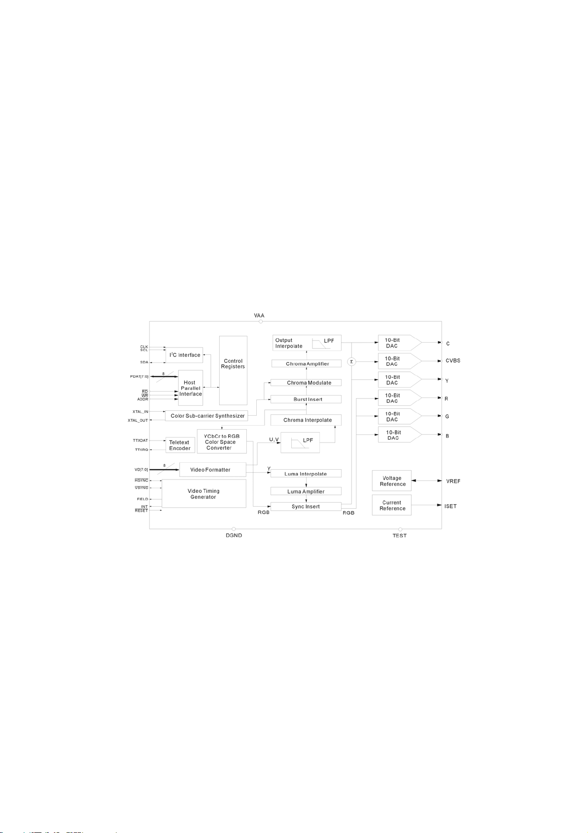
2-1-2 NTSC/PAL Digital Video Encoder (CS4955)
FEATURES
• Six DACs providing simultaneous composite, S-video,
and RGB or Component YUV outputs
• Programmable DAC output currents for low
imped-ance(37.5Ω) and high impedance(150
Ω)loads.
• Multi-standard support for NTSC-M, NTSC-JAPAN,
PAL (B, D, G, H, I, M, N, Combination N)
• ITU R.BT656 input mode supporting EAV/SAV codes
and CCIR601 Master/Slave input modes
• Porgrammable HSYNC and VSYNC timing
• Multistandard Teletext(Europe, NABTS, WST)
support
• VBI encoding support
• Wide-Screen Signaling (WSS) support,
EIA-JCPX1204)
• NTSC closed caption encoder with interrupt
• CS4955 supports Macrovision copy protection
Version 7
2
• Host interface configurable for parallel or I
C
compatible operation
• On-chip voltage reference generator
• +.3.3V or +5V operation, CMOS, low-power modes,
tri-state DACs
Ordering Information
CS4955-CQ 48-pin TQFP
DESCRIPTION
The CS4955 provides full conversion from digital video formats YcbCr or YUV into NTSC and PAL Composite,
Y/C (S-video) and RGB, or YUV analog video. Input formats can be 27MHz 8-bit YUV, 8-bit YcbCr, or
ITUR.BT656 with support for EAV/SAV codes. Video output can be formatted to be compatible with NTSC-M,
NTSC-J, PAL-B, D, G, H, I, M, N, and Combination N systems. Closed Caption is supported in NTSC. Teletext is
supported for NTSC and PAL.
Six 10-bit DACs provide two channels for an S-Video output port, one or two composite video outputs, and three
RGB or YUV outputs. Two-times oversampling reduces the output filter requirements and guarantees no DAC-ralated
modulation components within the specified bandwidth of any of the supported video standards.
Parallel or high-speed I
parallel interface doubles as a general purpose I/O port when the CS4954 is in I
board area.
6
2
C compatible conpatible control interfaces are provided for flexibility in system design. The
2
C mode to help conserve valuable
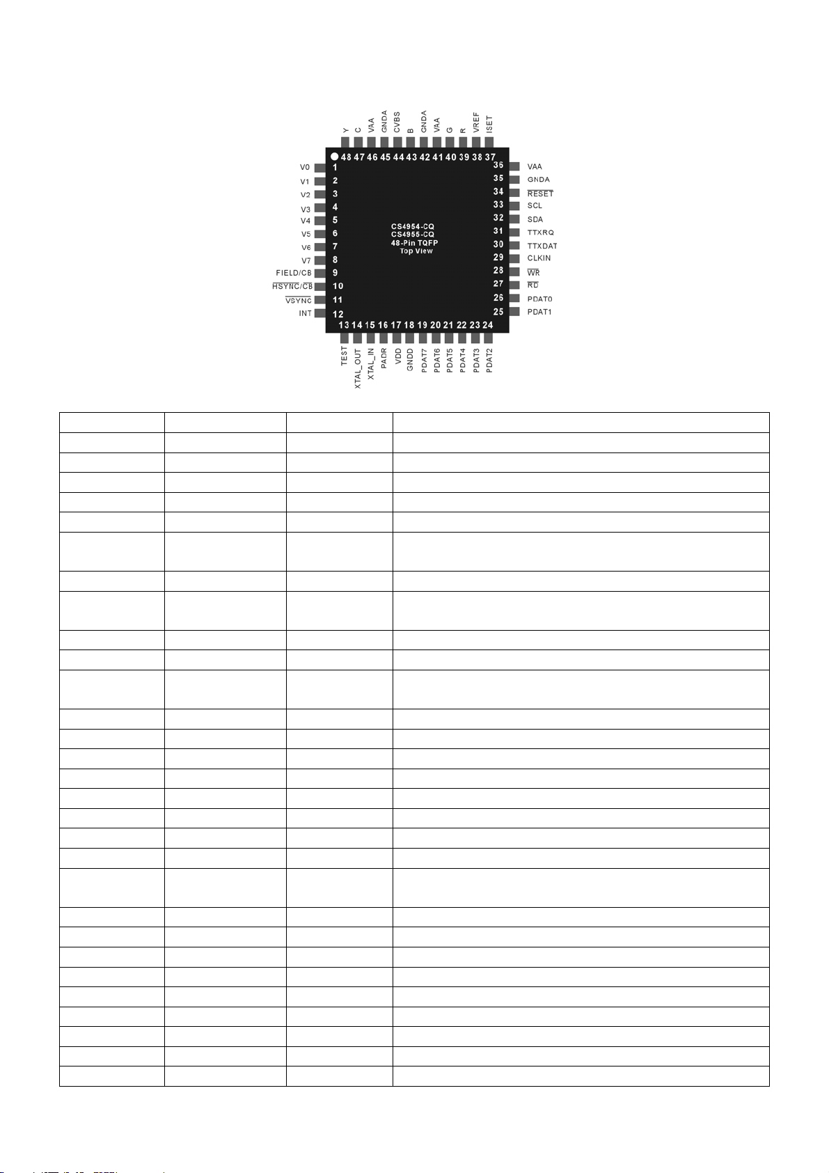
PIN DESCRIPTIONS
Pin Name Pin Number Type Description
V[7:0] 8,7,6,5,4,3,2,1 IN Digital video data inputs
CLK 29 IN 27MHz input clock
PADDR 16 IN Address enable line
XTAL_IN 15 IN Subcarrier crystal input
XTAL_OUT 14 OUT Subcarrier crystal input
HSYNC/CB 10 I/O Active low horizontal sync, or composite blank
signal
VSYNC 11 I/O Active low vertical sync
FIELD/CB 9 OUT Video field ID. Selectable polarity or composite
blank
RD 27 IN Host parallel port read strobe, active low
WR 28 IN Host parallel port write strobe, active low
PDAT[7:0] 19,20,21,22,23,
I/O Host parallel port/general purpose I/O
24,25,26
SDA 32 I/O I2C data
SCL 33 IN I2C clock input
CVBS 44 CURRENT Composite video output
Y 48 CURRENT Luminance analog output
C 47 CURRENT Chrominance analog output
R 39 CURRENT Red analog output
G 40 CURRENT Green analog output
B 43 CURRENT Blue analog output
VREF 38 I/O Internal voltage reference output or external
reference input
ISET 37 CURRENT DAC current set
TTXDAT 30 IN Teletext data input
TTXRQ 31 OUT Teletext request output
INT 12 OUT Interrupt output, active high
RESET 34 IN Active low master RESET
TEST 13 IN TEST pin. Ground for normal operation
VAA 36,41,46 PS +5V or +3.3V supply(must be same as VDD)
GNDD 18 PS Ground
VDD 17 PS +5V or 3.3V supply (must be same as VAA)
7

GNDA 35,42,45 PS Ground
2-1-3 DVD Processor Chip (MTK1369AE)
* Features
z Single-chip DVD video decoder in a 208-pin PQFP package
z Supports MPEG-1 system and MPEG-2 program streams
z Programmable multimedia processor architecture
z Compatible with Audio CD, Video CD, VCD 3.0, and Super Video CD (SVCD)
z DVD Navigation 1
z Built-in content Scrambling System (CSS)
- Audio
z Built-in Karaoke key-shift functio n
z DolbyTM Digital 2-channel down mix audio output for DolbyTM
z Dolby Pro Logic
z Linear PCM streams for24 bit / 96KHz
z Concurrent S/PDIF out and 2-channel audio output
z Sensaura Dolby Digital Virtual Surround
z DTS Digital Surround 2-channel down mix stereo output
z S/PDIF output for encoded AC-3, DTS Digital output or Linear PCM
- Peripheral
z Glueless interface to DVD loaders (ATAPI or A/V bus I/F)
z Bi-directional 12C audio interface
z 8 general-purpose auxiliary ports
z Single 27MHz clock input
- Smart Technology
z SmartZoomTM for motion zoom & pan
z SmartZoomTM for NTSC to PAL conversion and vice versa
SmartZoomTM for video error concealment
z
* Functional Description
8
* Pinout Diagram
9

10

PIN DESCRIPTON
PIN Symbol Type Description
1 IREF Analog Input
2 PLLVSS Ground Ground for data PLL and related analog circuitry
3 LPIOP Analog output Positive output of the low pass filter
4 LPION Analog output Negative output of the low pass filter
5 LPFON Analog output Negative output of loop filter amplifiter
6 LPFIP Analog input Positive input of loop filter amplifier
7 LPFIN Analog input Negative input of loop filter amplifier
8 LPFOP Analog output Positive output of loop filter amplifier
9 JITFO Analog output RF jitter meter output
10 JITFN Analog input Negative input of the operation amplifier for RF jigger meter
11 PLLVDD3 Power Power for data PLL and related analog circuitry
12 FOO Analog output Focus servo output. PDM output of focus servo compensator
13 TRO Analog output Tracking servo output.PDM output of tracking servo compensator
14 TROPENPWM Analog outpu
15 PWMOUT2 Analog outpu The general PWM output
16 DVDD2 Power 2.5V power
17 DMO Analog outpu Disk motor control output.PWM output
18 FMO Analog outpu Feed motor control. PWM output
19 FG Inout, pull up Motor Hall sensor input
20 DVSS Ground Ground
21 HIGHA0 Inout, pull up Microcontroller address 8
22 HIGHA1 Inout, pull up Microcontroller address 9
23 HIGHA2 Inout, pull up Microcontroller address 10
24 HIGHA3 Inout, pull up Microcontroller address 11
25 HIGHA4 Inout, pull up Microcontroller address 12
26 HIGHA5 Inout, pull up Microcontroller address 13
27 DVSS Ground Ground
28 HIGHA6 Inout, pull up Microcontroller address 14
29 HIGHA7 Inout, pull up Microcontroller address 15
30 AD7 Inout Microcontroller address/data 7
31 AD6 Inout Microcontroller address/data 6
32 AD5 Inout Microcontroller address/data 5
33 AD4 Inout Microcontroller address/data 4
34 DVDD3 Power 3.3V power
35 AD3 Inout Microcontroller address/data 3
36 AD2 Inout Microcontroller address/data 2
37 AD1 Inout Microcontroller address/data 1
38 AD0 Inout Microcontroller address/data 0
39 IOA0 Inout, pull up Microcontroller address 0/GPIO0
40 IOA1 Inout, pull up Microcontroller address 0/GPIO1
41 DVDD2 Power 2.5V power
42 IOA2 Inout, pull up Microcontroller address 0/GPIO2
43 IOA3 Inout, pull up Microcontroller address 0/GPIO3
44 IOA4 Inout, pull up Microcontroller address 0/GPIO4
45 IOA5 Inout, pull up Microcontroller address 0/GPIO5
46 IOA6 Inout, pull up Microcontroller address 0/GPIO6
47 IOA7 Inout, pull up Microcontroller address 0/GPIO7
48 A16 Outpu Flash address 16
49 A17 Output Flash address 17
50 IOA18 Inout Flash address 18 / GPIO10
51 IOA19 Inout Flash address 19 / GPIO11
52 DMVSS Ground Ground for DRAM clock circuitry
53 DMVDD3 Power Power for DRAM clock circuitry
Current reference input.it generate reference current for data PLL
Connect an external 100K resistor to this pin and PLLVSS.
Tray open output,co nt r ol l ed b y m i croco ntroller.
This is PWM output for TRWMEN
TRWMEN
27Hrw2=0
27hRW2=1 or is digital output for
11

PIN Symbol Type Description
54 ALE Inout,pull up Microcontroller address latch enable
55 IOOE# Inout Flash output enab le,active low /GPIO13
56 IOWR# Inout Flash write enable,active low /GPIO17
57 IOCS# Inout,pull up Flash chip select,active low /GPIO18
58 DVSS Ground Ground
59 UP1_2 Inout,pull up Microcontroller port 1-2
60 UP1_3 Inout,pull up Microcontroller port 1-3
61 UP1_4 Inout,pull up Microcontroller port 1-4
62 UP1_5 Inout,pull up Microcontroller port 1-5
63 UP1_6 Inout,pull up Microcontroller port 1-6
64 DVDD3 Power 3.3V power
65 UP1_7 Inout,pull up Microcontroller port 1-7
66 UP3_0 Inout,pull up Microcontroller port 3-0
67 UP3_1 Inout,pull up Microcontroller port 3-1
68 INT0# Inout,pull up Microcontroller in terrupt 0,active low
69 IR Input IR control signal input
70 DVDD2 Power 2.5V power
71 UP1_4 Inout Microcontroller port 3-4
72 UP1_5 Inout Microcontroller port 3-5
73 UWR# Inout,pull up Microcontroller write strobe,active low
74 URD# Inout,pull up Microcontroller read strobe,active low
75 XTALI Input Crystal input,27MHz
76 XTALO Output Crystal output
77 DVSS Ground Ground
78 RD7 Inout DRAM data 7
79 RD6 Inout DRAM data 6
80 RD5 Inout DRAM data 5
81 RD4 Inout DRAM data 4
82 DVDD2 Power 2.5V power
83 RD3 Inout DRAM data 3
84 RD2 Inout DRAM data 2
85 RD1 Inout DRAM data 1
86 RD0 Inout DRAM data 0
87 RWE# Output DRAM write enable,active low
88 CAS# Output DRAM column address strobe,active low
89 RAS# Output DRAM row address strobe,active low
90 RCS# Output DRAM chip select,active low
91 BA0 Output DRAM bank address 0
92 DVDD3 Power 3.3V power
93 RD15 Inout,pull up/down DRAM data 15
94 RD14 Inout,pull up/down DRAM data 14
95 RD13 Inout,pull up/down DRAM data 13
96 RD12 Inout,pull up/down DRAM data 12
97 DVSS Ground Ground
98 RD11 Inout,pull up/down DRAM data 1 1
99 RD10 Inout,pull up/down DRAM data 10
100 RD9 Inout,pull up/down DRAM data 9
101 RD8 Inout,pull up/down DRAM data 8
102 VPVDD3 Power Power for varipitch VCO circuitry
103 VCOCIN Analog input Connect capacitor for compensator loop filter
104 VPVSS Ground Ground for varipitch VCO circuitry
105 DVSS Ground Ground
106 CLK Output DRAM clock
107 CLE Output DRAM clock enable
108 RA11 Output DRAM address bit 11 or audio serial data 3 (channel 7/8)
109 RA9 Output DRAM address 9
110 RA8 Output DRAM address 8
111 DVDD2 Power 2.5V power
112 RA7 Output DRAM address 7
12
 Loading...