

Page 1
SERVICE MANUAL
Customer Model:
PDP4206EM
Safety Precaution
Technical Specifications
Block Diagram
Circuit Diagram
Basic Operations & Circuit Description
Main IC Specifications
Product Specification of PDP Module
Trouble Shooting Manual of PDP Module
Spare Part List
Exploded View
If you forget your V-Chip Password
Software Upgrade
This manual is the latest at the time of printing, and does not
include the modification which may be made after the printing,
by the constant improvement of product.
Page 2

Safety Precaution
CAUTION
RISK OF ELECTRIC SHOCK
DO NOT OPEN
A
CAUTION: TO REDUCE THE RISK OF
ELECTRIC SHOCK, DO NOT REMOVE COVER
(OR BACK). NO USER-SERVICEABLE PARTS
INSIDE. REFER SERVICING TO QUALIFIED
SERVICE PERSONNEL ONLY.
A
The lightning flash with arrowhead symbol,
within an equilateral triangle, is intended to
alert the user to the presence of uninsulated
“dangerous voltage” within the product’s enclo
sure that may be of sufficient magnitude to
constitute a risk of electric shock to persons.
The exclamation point within an equilateral
triangle is intended to alert the user to the
presence of important operating and
maintenance (servicing) instructions in the
literature accompanying the appliance.
PRECAUTIONS DURING
SERVICING
1. In addition to safety, other parts and
assemblies are specified for conformance with
such regulations as those applying to spurious
radiation. These must also be replaced only
with specified replacements.
Examples: RF converters, tuner units, antenna
selection switches, RF cables, noise-blocking
capacitors, noise-blocking filters, etc.
2. Use specified internal Wiring. Note especially:
1) Wires covered with PVC tubing
2) Double insulated wires
3) High voltage leads
3. Use specified insulating materials for hazardous
live parts. Note especially:
1 ) Insulating Tape
2) PVC tubing
3) Spacers (insulating barriers)
4) Insulating sheets for transistors
5) Plastic screws for fixing micro switches
4. When replacing AC primary side components
(transformers, power cords, noise blocking
capacitors, etc.), wrap ends of wires securely
about the terminals before soldering.
5. Make sure that wires do not contact heat
generating parts (heat sinks, oxide metal film
resistors, fusible resistors, etc.)
6 . Check if replaced wires do not contact sharply
edged or pointed parts.
7. Make sure that foreign objects (screws, solder
droplets, etc.) do not remain inside the set.
MAKE YOUR CONTRIBUTION
TO PROTECT THE
ENVIRONMENT
Used batteries with the ISO symbol
\5<9
for recycling as well as small accumulators
(rechargeable batteries), mini-batteries (cells) and
starter batteries should not be thrown into the
garbage can.
Please leave them at an appropriate depot.
WARNING:
Before servicing this TV receiver, read the
SAFETY INSTRUCTION and PRODUCT
SAFETY NOTICE.
SAFETY INSTRUCTION
The service should not be attempted by anyone
unfamiliar with the necessary instructions on this
apparatus. The following are the necessary
instructions to be observed before servicing.
1. An isolation transformer should be connected in
the power line between the receiver and the
AC line when a service is performed on the
primary of the converter transformer of the set.
2. Comply with all caution and safety related
provided on the back of the cabinet, inside the
cabinet, on the chassis or picture tube.
3. To avoid a shock hazard, always discharge the
picture tube's anode to the chassis ground
before removing the anode cap.
4. Completely discharge the high potential voltage
of the picture tube before handling. The picture
tube is a vacuum and if broken, the glass will
explode.
Page 3

5. When replacing a MAIN PCB in the cabinet,
always be certain that all protective are
installed properly such as control knobs,
adjustment covers or shields, barriers, isolation
resistor networks etc.
6 . When servicing is required, observe the original
lead dressing. Extra precaution should be given
to assure correct lead dressing in the high
voltage area.
7. Keep wires away from high voltage or high
tempera ture components.
8 . Before returning the set to the customer,
always perform an AC leakage current check
on the exposed metallic parts of the cabinet,
such as antennas, terminals, screwheads, metal
overlay, control shafts, etc., to be sure the set
is safe to operate without danger of electrical
shock. Plug the AC line cord directly to the
AC outlet (do not use a line isolation
transformer during this check). Use an AC
voltmeter having 5K ohms volt sensitivity or
more in the following manner.
Connect a 1.5K ohm 10 watt resistor paralleled
by a 0.15pF AC type capacitor, between a
good earth ground (water pipe, conductor etc.,)
and the exposed metallic parts, one at a time.
Measure the AC voltage across the combination
of the 1.5K ohm resistor and 0.15 uF
capacitor. Reverse the AC plug at the AC
outlet and repeat the AC voltage m easurements
for each exposed metallic part.
The measured voltage must not exceed 0.3V
RMS.
This corresponds to 0.5mA AC. Any value
exceeding this limit constitutes a potential
shock hazard and must be corrected
immediately.
The resistance measurement should be done
between accessible exposed metal parts and
power cord plug prongs with the power switch
"ON". The resistance should be more than
6 M ohms.
AC VOLTMETER
PRODUCT SAFETY NOTICE
Many electrical and mechanical parts in this
apparatus have special safety-related
characteristics.
These characteristics are offer passed
unnoticed by visual spection and the protection
afforded by them cannot necessarily be obtained
by using replacement components rates for a
higher voltage, wattage, etc.
The replacement parts which have these
special safety characteristics are identified by A
marks on the schematic diagram and on the parts
list.
Before replacing any of these components,
read the parts list in this manual carefully. The
use of substitute replacement parts which do not
have the sam e safety characteristics as specified
in the parts list may create shock, fire, or other
hazards.
9. Must be sure that the ground wire of the AC
inlet is connected with the ground of the
apparatus properly.
Good earth ground
such as the water
- p ipe , con d u cto r,
etc.
AC Leakage Current Check
1500 ohmi, lOwatt
Place this probe
on each exposed
metallic part
Page 4
Technical Specifications
MODEL : PDP4206EM
42" Plasma Monitor
DATE FIRST ISSUED ISSUE
1
REVISIONS
ISSUED DATE DESCRIPTION RAISED BY :
RAISED BY CHECKED BY NUMBER OF PAGES
9
SPECIFICATION AGREED : SIGNATURE DATE
R & D DEPARTMENT
COMMERCIAL DEPARTMENT
PRODUCTION DEPARTMENT
Q/A DEPARTMENT
CUSTOMER
SPECIFICATION APPROVED : SIGNATURE : DATE
N O T E : Only d o cu m e n ts s tam p e d “C o ntro lled D o c u m en t” to b e u sed for m a n ufacture o f p roduction parts.
Page 5

CONTINUATION PAGE
Technical Specifications
PDP420
NUMBER 2 OF 9 PAGES
1. Standard Test Conditions
All tests shall be performed under the following conditions, unless otherwise specified.
1.1 Ambient light
1.2 Viewing distance :
1.3 Warm up time :
1.4 PDP Panel facing :
1.5 Measuring Equipment :
1.6 Magnetic field :
1.7 Control settings :
1.8 Power input :
1.9 Ambient temperature :
1.10 Display mode :
150ux (When measuring IB, the ambient luminance
^0.1Cd/m2)
50cm in front of PDP
30 minutes
no restricted
PC, Chroma 2225 signal generator (with Chroma digital
additional card) or equivalent, Minolta CA100 photometer
no restricted
Brightness, Contrast, Tint, Color set at Center(50)
110~120Vac
20°C ± 5°C (68°F ± 9°F)
31.5KHz/60Hz (Resolution 852 x 480)
1.11 Other conditions :
1.11.1 With image sticking protection of PDP module, the luminance will descend
by time on a same still screen and rapidly go down in 5 minutes. When
measuring the color tracking and luminance of a same still screen, be sure
to accomplish the measurement in one minute to ensure its accuracy.
1.11.2 Due to the structure of PDP, the extra-high-bright same screen should not
hold over 5 minutes for fear of branding on the panel.
Page 6

Technical Specifications
ELECTRICAL CHARACTERISTICS
2. Power Input
PDP4206EM
CONTINUATION PAGE
NUMBER 3 OF 9 PAGES
2.1 Voltage
2.2 Input Current
2.3 Maximum Inrush Current
Test condition
2.4 Frequency
2.5 Power Consumption
Test condition
2.6 Power Factor
2.7 Withstanding voltage
3. Display
3.1 Screen Size
3.2 Aspect Ratio
3.3 Pixel Resolution
3.4 Peak Brightness
3.5 Contrast Ratio (Dark room)
3.6 Viewing Angle
3.7 OSD language
110 ~120VAC
3.5 / 1.5A
<30 A (FOR AC110V ONLY)
Measured when switched off for at least 20 mins
50Hz to 60Hz(±3Hz)
< 330W
full white display with maximum brightness and
contrast
Meets I EC 1000-3-2
1.5kVac or 2.2kVdc for 1 sec
42” Plasma monitor
16:9
852x480
1000 cd/m2 (Panel module without filter)
3000:1 (Panel module without filter)
Over 160°
English
4. Signal
4.1 AV & Graphic input
4.1.1 Composite signal
4.1.2 Y,C Signal
4.1.3 Component signal
4.1.4 Graphic I/P
4.1.5 PnP compatibility
4.1.6 I/P frequency
CVBS
S-Video
Y, Pb/Cb, Pr/Cr, HDTV compatible
Analog: D-sub 15pin detachable cable
Digital: DVI
DDC 1.0
fH 31.5kHz to 60kHz/fV: 56.25Hz to 75Hz (640x480
recommended)
Page 7

Technical Specifications
4.2 Audio input
Audio I/P(L/Rx5)
4.3 Audio output
Audio O/P(L/Rx1) :
PDP4206EM
1 for DVI / D-Sub
1 for Y/ Pb/Pr
1 for Y/ Cb/Cr
1 for Video
1 for S-Video
1 for Line out
CONTINUATION PAGE
NUMBER 4 OF 9 PAGES
4.4 Other function :
5. Environment
5.1 Operating environment
5.1.1 Temperature :
5.1.2 Relative humidity:
5.2 Storage and Transport
5.2.1 Temperature :
5.2.2 Relative humidity:
6. Panel Characteristics
6.1 Type :
6.2 Size :
6.3 Aspect ratio
6.4 Viewing angle
6.5 Resolution
6.6 Weight
6.7 Color
6.8 Contrast
6.9 Peak brightness :
PIP, 16:9, 4:3, Zoom
5°C ~ 33°C
20% ~ 85%(non-condensing)
-20°C to 60°C(-4° to 140°F)
5% to 95%
LG V6
42”, 1005mm(width)x597mm(height)x61 mm(depth)±1
mm)
16:9
Over 160°
852x480
14.8kg ±0.5 kg (Net)
16.77 million colors by combination of 8 bits R,G,B digital
Average 60:1 (In a bright room with 150Lux at center)
Typical 3000:1 (In a dark room 1/25 White Window
pattern at center).
Typical 1000cd/m2 (1/25 White Window)
6.10 Color Coordinate Uniformity :
Test Pattern :
Contrast; Brightness and Color control at norma
setting
Full white pattern
Average of point A,B,C,D and E +/- 0.01
Page 8

CONTINUATION PAGE
Technical Specifications
PDP4206EM
NUMBER 5 OF 9 PAGES
6.11 Color temperature : Contrast at center (50); Brightness center (50);
Color temperature set at Natural
x=0.285±0.02
y=0.293±0.02
6.12 Cell Defect Specifications
Subject to Panel supplier specification as appends.
7. Front Panel Control Button
7.1 SEL. UP/Down Button : Push the key to selecting the item on OSD menu
Volume Up/ Down Button : Push the key to increase the volume up or down.
When selecting the adjusting item on OSD menu
increase or decrease the data-bar.
Menu Button : Enter to the OSD menu.
Input Select Button : Push the key to select the input signals source.
7.2 Stand by Button : Switch on main power, or switch off to enter power
Saving modes.
7.3 Main Power Switch : Turn on or off the unit.
8. OSD Function
8.1 Audio : Adjust or Select Volume; Bass; Treble; Balance; SRS; BBE; AVC;
Int./Ext. Speaker.
8.2 Picture : Adjust or Select Brightness; Contrast; Sharpness; Scaling (Picture
changes According to Fill or One to One.; DNR; Video Format;
More options for Y/Pb/Pr and VGA ( H. Position, V. Position Phase,
Frequency)
8.3 OSD : Position; OSD H. Position; OSD V. Position; OSD Timeout;
OSD Backgroud; Language.
8.4 Tools : Factory Reset; Source Scan; Blank Color; Turn Off Timer; Screen
Saver; Saver Mode.
8.5 CC-V Chip : TV Channel Blocking; Movie Blocking; Change Blocking Password;
Clear Password; CC Mode; CC Background.
Page 9

CONTINUATION PAGE
Technical Specifications
PDP4294LV1
NUMBER 6 OF 9 PAGES
9. Agency Approvals
Safety UL60950
Emissions FCC class B
10. Reliability
11.1 MTBF : 20,000 hours(Use moving picture signal at 25°C ambient)
11. Accessories : User manual x1, Remote control x1, Stand x1, Power cord x1.
Battery x 2, Accessories box x 1.
Page 10

Technical Specifications
PDP4206EM
NUMBER 7 OF 9 PAGES
12. Supportthe Signal Mode
The PDP can support the different from DVI or VGA Signal Mode in 24 kinds
CONTINUATION PAGE
NO. Resolution Horizontal
Frequency
(KHz)
Vertical
Frequency
(Hz)
Dot Clock
Frequency
(MHz)
1# 640 x400 31.47 70.08 25.17
2# 640 x400 37.90 85.00 31.5
3 640 x480 31.50 60.00 25.18
4 640 x480 35.00 67.00 30.24
5 640 x480 37.50 75.00 31.50
6 640 x480 37.86 72.81 31.50
7# 640 x480 43.30 85.00 36.00
8 800 x600 35.16 56.25 36.00
9 800 x600 37.90 60.32 40.00
10 800 x600 46.90 75.00 49.50
11 800 x600 48.08 72.19 50.00
12 800 x600 53.70 85.00 56.25
13 832 x624 49.00 75.00 57.27
14 1024 x768 48.40 60.00 65.00
15 1024 x768 56.50 70.00 75.00
16 1024 x768 60.00 75.00 78.75
17 1024 x768 68.70 85.00 94.50
18* 1152x864 54.53 60.00 80.37
19 1152x864 67.52 75.02 108.03
20* 1152x864 63.86 70.02 94.51
21 1280x1024 63.37 60.01 111.51
22 1280 x960 75.02 75.02 126.00
23 1280 x960 60.02 60.02 108.04
24# 1280x720 44.96 59.95 74.19
Note: DVI could not support * of signal mode.
VGA could not support # of signal mode.
- Press "DISPLAY” button to confirm the input signal format.
Note: Some data will be updated in five seconds if you change them.
Page 11

Technical Specifications
13. Remote Function+
PDP4206EM
CONTINUATION PAGE
NUMBER 8 OF 9 PAGES
Mute
YPbPr
PC
C/C -
VOL +/-
Menu Left/Right
Up/Down
Left/Right
Button
SRS
ZOOM plus/minus
Display
Sleep
Standby on/off
PIP
Video
Number Buttons/
Channel up/
Channel down/
Return
V-CHIP
EXIT Button
Input
BBE
Wide
Freeze
F.WHITE
AUTO
Page 12

Technical Specifications
PHYSICAL CHARACTERISTICS
14. Power Cord
PDP4206EM
CONTINUATION PAGE
NUMBER 9 OF 9 PAGES
Length :
Type :
15. Cabinet
15.1 Color :
15.2 Weight (with stand)
Net weight : 84.5lbs (38.3kg)
15.S Dimensions(with stand)
Width
Height
Depth
1.8m nominal
optional
“Black” colour as defined by colour plaque reference number
40-7/8 inches (1040mm)
27-1/4 inches (692mm)
11-1/4 inches (286mm)
Page 13
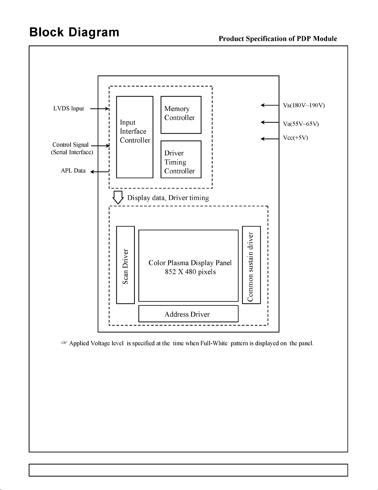
Block Diagram
Product Specification of PDP Module
LVDS Input
Control Signal —
(Serial Interface)
APL Data
Memory
Input
Controller
Interface
Controller
Driver
Timing
Controller
Display data, Driver timing
>
•c
Q
GO
G
cd
O
Color Plasma Display Panel
852 X 480 pixels
•G
T3
O
Vs(180V~190V)
Va(55V~65V)
Vcc(+5V)
<u
>
cö
3
c
O
a
a
o
Address Driver
Applied Voltage level is specified at the time when Full-White pattern is displayed on the panel.
Page 14
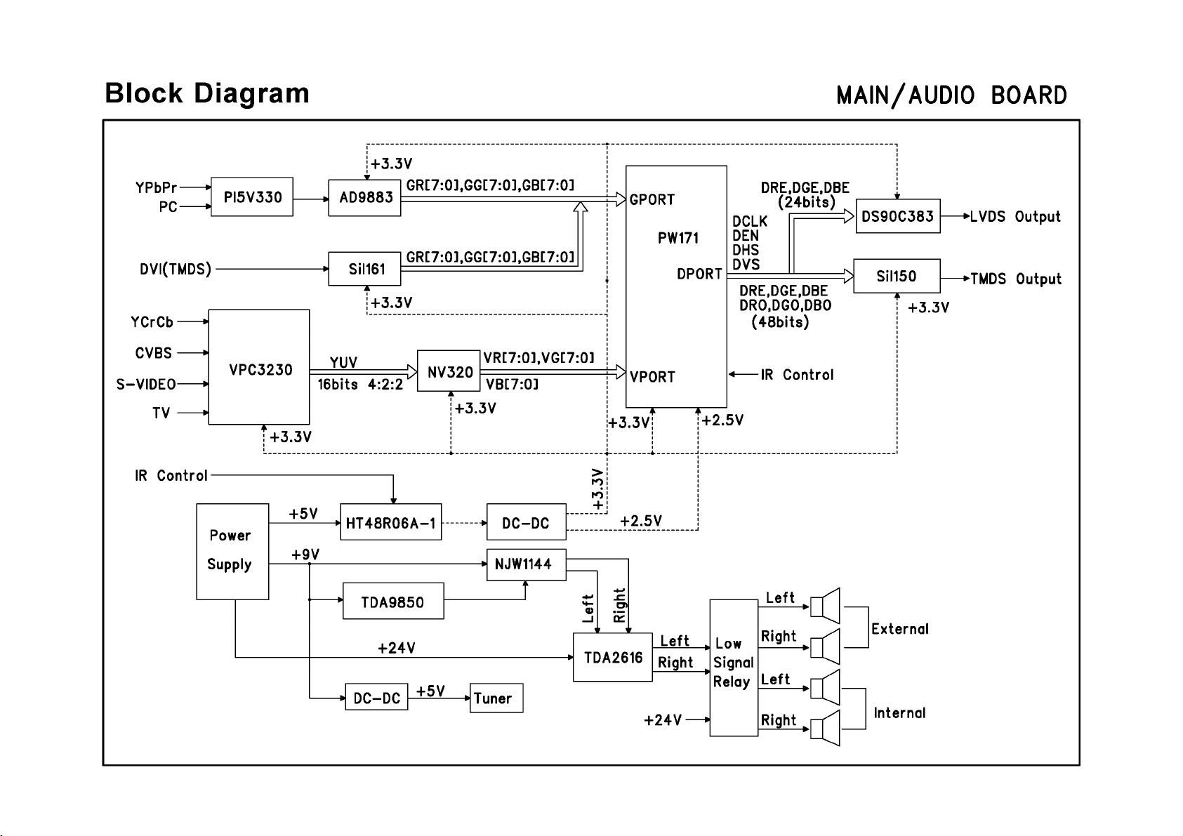
Block Diagram
M A IN / A U D IO BOARD
Page 15
Circuit Diagram
- Power supply board of PDP Module,
- Power supply board of PDP Module,
- Main (Video) board
- Audio/Tuner board
- Keypad board
- Remote control receiver board
- External L/R Speakers board
- Remote control board
Page 16
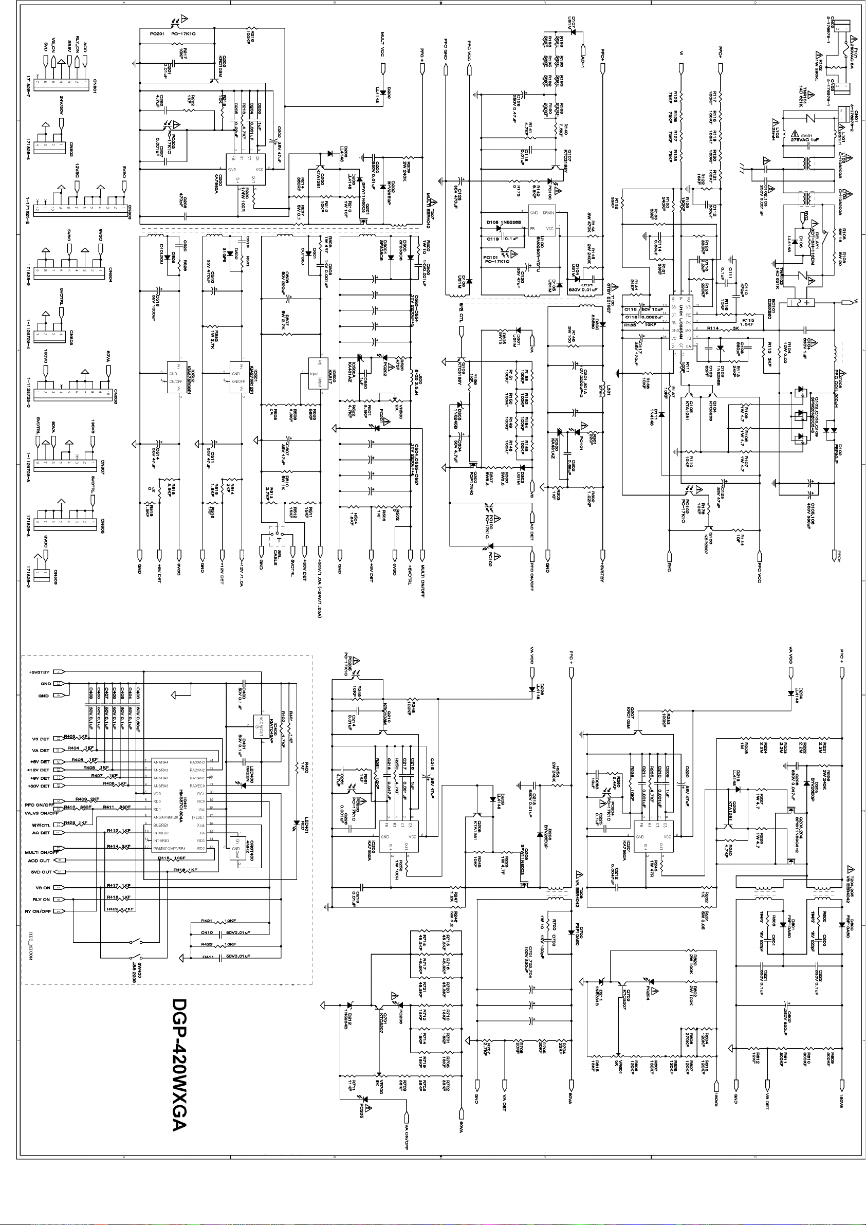
DGP-420WXGA
USP490M-42LP
Page 17
Page 18
□ LIVE
| | NEUTRAL Q 100VDC | | REFERENCE
□ rG
NOTE : VALUE FOR ALL CAPACITOR ARE IN uF. ELSE SPECIFY.
RATED WATTAGE FOR ALL RESISTOR ARE 1/10W. ELSE SPECIFY.
LAST NO :
Q 0 - 30VD 1 1 300VDC
| | 150V
1
-----
1 PULS VOLTAGE
| | SECONDRAY
CON-171825-9 C0N-GP39Q-04P-TS
60VA [
5VCTRL
C0N-GP390-10P-TS CON-1-1123723-8
CON—171825—8
CON-171825-2
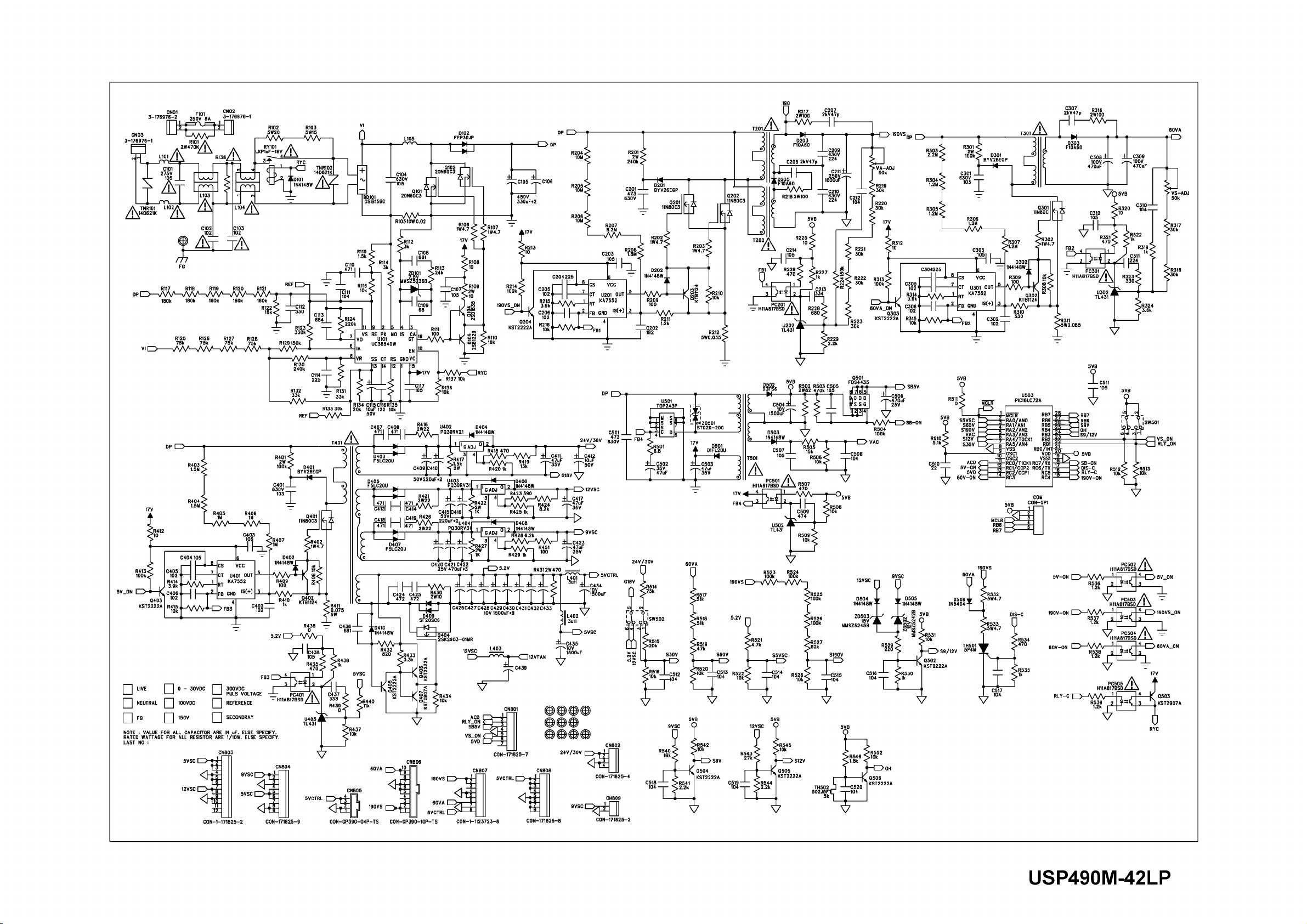
USP490M-42LP
Page 19

NPUT AFE
D
VCP3230
VVINT VUV[7:0] <
CB VVHS
RESETn VY[7:0] *
Y
SDA SCL
CR VVVS
STBLED VFIELD
POWER ON
05_VCP3230
TMDS
► DBO[7:0]
DHS
DENG
DENR
► DGE[7:0]
► DRE[7:0]
► DGO[7:0]
► DRO[7:0]
DCLK
DVS
9_DERB
► DBE[7:0]
VVCLK
MUTE
MUTE1
IR
NV320
SDA VG[7:0]
SCL VB[7:0]
VVHS VR[7:0]
RESETn VCLK
VVCLK VVS
NDSP_EN VHS
VY[7:0]
VUV[7:0]
VVVS
MISC
LED-G
ICSSTM
ICSCLK
ICSSTD
LED-R
ICSDAT
TXD
RDn
► D[7:0]
CS1n
STBLED
DVI PW171
RXCm
RX0m GPEN
RX1p GBE[7:0]
RX1m GVS
RX0p GBO[7:0]
GDFEOE GFBK
RX2m GHS
RX2p GGE[7:0]
RXCp GCLK
G
RE
GRO[7:0]
GGO[7:0]
HDCBIN
HDYIN GRE[7:0] 4 1
GAFEOE GHS
VGASEL GCLK
GVSYNC GFBK
GCOAST GGE[7:0] 4
HDCRIN GVS
GRAIN
SCL
GBAIN
GBLKSPL
GGAIN
SDA
GHSYNC
GBE[7:0] 4
► D[15:0] DGE[7:0]
► A[19:0] DRO[7:0]
► VR[7:0] GCOAST
► VG[7:0] ROMOEn
► VB[7:0] TXD
► GRE[7:0] DENG
► GBO[7:0] DENR
► GBE[7:0] DHS
► GGO[7:0] SCL
► GRO[7:0]
► GGE[7:0]
8-IRWÜVR1
MEMORY
VPEN
► NDSP EN
POWER LVDS
DCKEXT
MCKEXT
RXD
RESET
RESETn
POWER_ON
IRRCVR1
NMI
DENG
DCLK
DVS
DHS
DTXON
RESET-2
SCL
SDA
CPUGO
PDPGO
PDWN
IRQ
DGE[7:0]
DRE[7:0]
DBE[7:0]
SDA DBE[7:0]
GFBK DGO[7:0]
CS1n DRE[7:0]
VPPEN DBO[7:0]
RDn DCLK
NMI GBLKSPL
VCLK ROMWEn
GHS DVS
GCLK DENB
GVS
MCKEXT
RXD
RESET
DCKEXT
VPEN
VVS
VFIELD
GPEN
ICSCLK
ICSSTD
ICSSTM
ICSDAT
LED-R
LED-G
DTXON
VGASEL
GAFEOE
GDFEOE
VVINT
VHS
MUTE
SLEEP1
PIO3
CPUGO
PDPGO
RESET-2
PDWN
IRQ
C
B
A A
Page 20

( o a p iA ) u ie|/M
»a d o<
>r o o<
[ozldao
[o zü o o
dnzi?
6t?o"
dnU o
8K )
I
K3 10S Z£62IAn
/ 9390
f q^ao"
0390 81-dd
¿300
/ 9 300
/ S 300
/ fr300 Zl-dd
/ £30 0
/ ¿300
/"
/ 93UO
/------------
/ fr3M0 Sí-dd
f £3HO
1-3H0
dn U'O
9n
ZfrO
91-dy
H d ü
dnZfr
9frO~
s a o v
oos a v
s h o v
UZfr
1
»o a v
zaav
9a av
9a av
*a av
UZfr
eaav
zaav
i-aav
azi? oaav
zo av
9o av
9o av
UZfr i^oav
eo av
zo av
i-oav
azi? o oav
zu av
9d av
9d av
Kj av
eu av
zu av
i-uav
uzt? o ua v
dn U'O
91?0
K T, T, T , T , n
O C l O O O O O O O O O O O ílO O
z z z z z z z ~ z . z z z z z z z z
in osA
w
ino o o s
99
in o sH
99
Z9
Z3 ma
CV
93 m a
k-‘l-
93 m a
VV
r a m a
b V
fa m a
91-
23 m a
Zl-
□ m a
81-
03 m a
tíl-
ZN33UO
C
9N33UO
k-‘
SN33dO
V
WM33dO
y
£N33dO
9
3N33UO
Z
I.N33UO
8
ON33UO
b
Z03U
OZ
903U
l-Z
903U
CL
K]3d
17
ca3d
VL
203d
y¿
IQ 3 Ü
9 Z
0Q3U
-o-o < << < < <
<< o oo oo o
oo o o o oo o
K 310S Z£62IAn
9Í1
OH VE8860V
dn|/0
PPO
3 0 0 0
o o o o
z z z z
o p o o
AOSailAI
dA3d3d
0N A SA
0NA SH
NIOOS
ÑIVO
jn |.
890
O | jn|. o
T
1-0 |
jn|. O
990 I
T
30
3N
1-0 I
dn|/0
1-90 I
”1
O | jni- Q |
7 jn|,^~|~jn1,0 I jn|- 0 I jn|- 0 I jn|-ó~l~jrH 0 I
)“ J “ Z 9 0^ 990 990 ^ t?90^ £90 ^ 2 90^
O | dni-'O | dnl- q"| dni- Q | dn|, O | dn|-0 | dn|-p " |~dn|- O | dnl O | dn|/Q |
dn l-
oj~ i*oj^ oT 6eo^ 8eo^ zco^ 9co^ 9eo^ teo^
e to
q q a v q q a v q q a v q q a v q q a v q q a v q q a v q q a v q q a v q q a v
dnk
1-90
T *T
aa A d a aAd
1 NIV30
1 N IVO O
1 NIVd O
NiaoaH
NIAOH
N m o a H
Page 21

OVCCOCVCC PVCCoAVCC
OO OOO oocJ
9e
90
91
8S
se
80
81
93
94
4
1
7
3
9
2
99
CCCCC CCC
VVVVV VVV
OOOOO
RXOp
RXOm
RX ip
RX im
RX2p
RX2m
RXCp
RXCm
OCK_INV
PIXS
DFO
STAG_OUT
ST
PDO
PD
RSVD
DDDDD i23
NNNNN DDD
GGGGG NNN
OOOOO GGG
SIIiei
U4
D
RXOp
RXOm
RX ip
RXim
RX2p
RX2m
RXCp
RXCm
GDFEOE
AVCC
RiS
SiO
SIRES GGEi
&
OVCC
o
100
___
___
__
COCO CO 03
CCCC
CCCC
DDDDD
o
SISCDT
SCDT
QEO
QEi
QE2
QE3
QE4
QES
QEe
QE7
QE8
QE9
QEiO
QE11
QE i2
QE i3
QEi4
QE iS
QEie
QE i7
QE18
QE i9
QE2O
QE2i
QE22
QE23
QOO
QOi
QO2
QO3
QO4
QOS
QOe
QO7
QO8
QO9
QOiO
QO11
QO i2
QO i3
QOi4
QO iS
QOie
QO i7
QO18
QO i9
QO2O
QO2i
QO22
QO23
ODCK
VSYNC
HSYNC
CTLi
CTL2
CTL3
8
SIBEO RP1
10
SIBE1
11
SIBE2
12
SIBE3
SIBE4 RP2
14
SIBE5
is
SIBEe
ie
SIBE7
17
SIGEO RP3
20
SIGE1
21
SIGE2
22
SIGE3
23
SIGE4 RP4
24
SIGE5
25
SIGEe
2e
SIGE7
27
SIREO RP5
30
SIRE1
31
SIRE2
32
SIRE3
33
SIRE4 RPe
34
SIRE5
35
SIREe
3e
SIRE7
37
SIBOO RP7
49
SIBO1
50
SIBO2
51
SIBO3
52
SIBO4 RP8
53
SIBO5
54
SIBOe
55
SIBO7
se
SIGOO RP9
59
SIGO1
60
SIGO2
ei
SIGO3
e2
SIGO4 RP10
e3
SIGO5
e4
SIGOe
es
SIGO7
ee
SIROO RP11
e9
SIRO1
70
SIRO2
71
SIRO3
72
SIRO4 RP12
73
SIRO5
74
SIROe
75
SIRO7
77
SICLK RP13
44
SIDE
4e
DE
SIVS
47
SIHS
48
40
42
Q TP1
N/S/
'S/S/*
N/V*
N/S/
N/S/
N/S/-
N/S /
N/V*
N/S/
N/S/
N/S/-
w
'S/S/*
N/S/
N/S/
N/S/
'S/S/*
w
'S/S/*
w
w
N/S/
'S/S/ '
N/S/
w
N/S/^
'S / S/
N/S /
N/S /
w
N/S/
N/S/
N/S/
N/S/
N/S/
N/S/
N/S/
47R GBEO
47R GBE4
47R GGEO
GGE2
GGE3
47R GGE4
GGES
GGEe
GGE7
47R GREO
GREi
GRE2
GRE3
47R GRE4
GRES
OREO
GRE7
47R GBOO
GBOi
GBO2
GBO3
47R GBO4
GBOS
GBOe
GBO7
47R GGOO
GGOi
GGO2
GGO3
47R GGO4
GGOS
GGOe
GGO7
47R GROO
GROi
GRO2
GRO3
47R GRO4
GROS
GROe
GRO7
47R
GBE[7:O]
GGE[7:O]
GRE[7:O]
GBO[7:O] C
GGO[7:O]
GRO[7:O]
TP2 TP3 TP4 TPS TPe
0 0 0
u
VCC
o
C14
OiuF
V33T LiS OVCC
FB_42O_OHM_2OOMA Ç
_______
Î
V33T Lie CVCC
FB_42O_OHM_2OOMA 9
_______
t
V33T Li7 PVCC
FB_42O_OHM_2OOMA 9
_______
Î
V33T L18 AVCC
FB_42O_OHM_2OOMA 9
_______
Î
GCLK
GPEN
GVS
GHS
GFBK
U3
LM2937 _SOT223
VI
DNG
TAB
rv~\________________
rv~\________________
rv~\
_____________
- Î
rv~\________________
O
V
Ci7
iOuF
C23
iOuF
C27
C27 C2
iOuF
C29
iOuF
CiS
Cie
OiuF
47uF
OVCC OVCC OVCC OVCC OVCC
I C18 C19 I C20 I C21 I C22
V M V V
I O iu F |~0 1uF |~0 1uF I O iu F j O iu F
CVCC CVCC CVCC
V V 1
C24 C2S C2e
j O iu F j O iu F j O iu F
PVCC
j O iu F
AVCC AVCC AVCC AVCC
M M
I C30 C31 I C32 I C33
j O iu F |~0 1uF |~0 1uF j 0 1u
B
rocou^co cd
A
A
Main (Video)
Page 22

V33
o
ROMOEn
-O 1
JP1
3
ROMWEn
R69
3.3K
FWPn
A1
A2
A3
A4
Ab V33
A6 U17
A7
A8
A9
A10
A11
A12
A13
A14
A1b
A16
A17
A18
A19
R70 < R 71
3.3K 3.3K
D
V33
VPPEN
U16
CE
OE
WE
RP
WP
BYTE
A0
A1
A2
A3
A4
A5
A6
A7
A8
A9
A10
A11
A12
A13
A14
A15
A16
A17
A18
V33
VPP
VCC
D1
D2
D3
D4
D5
D6
D7
D8
D9
D10
D11
D12
D13
D14
D15
D16
GND1
GND2
?
C16
V33
D0
D1
D2
D3
D4
D5
D6
D7
D8
D9
D10
D11
D12
D13
D14
D15
FCEn
o
R68^ ^ v J 0K VP1 1
1
CEn
VPPON
P2
132
V33
4
13
29
33
35
38
40
42
44
30
32
34
36
39
41
43
45
46
27
VPP 3 390 6 2
---------
C167
22uF
Q4
VP3
VP2
R67
1K
Q5
3904
V33
SCL
SDA
6 8
SCL VCC
SDA
NC0 WP
2
NC1
3 4
NC2 GND
24C16
7
C168
0.1uF
C
VCC
O
A2 A1
A4 A3
A6 Ab
A9
A11 A10
A12
A14 A13
A17 A16
A19 A18
ROMOEn ROMWEn
A A
A[19:1] [
D15 D7
D14 D6
D5 D12
D4
D3 D10
D2
D9
D8 D0
JP3
VCC
o
IRPn R72
IA20 R74
IA21 R7
V33
o
A7
A8
A15
D13
D1
Main (Video)
B
Page 23

D
C
A A
Main (Video)
Page 24

SDA
SCL
V33 V33 V33 V33 V33
DRE[7:O]
D
DGE[7:O]
DBE[7:O]
DRE[7:O]
DGE[7:O]
DBE[7:O]
DREO 47R
DREi
DRE2
DRE3
DRE4
DRE5
DREe
DRE7
DGEO 47R
DGEi
DGE2
DGE4
DGE5
DGEe
DBEO 47R
DBEi
DBE2
DBE3
DBE4
DBE5
DBEe
DREO 47R
DREi
DRE2
DRE3
DRE4 47R
DRE5
DREe
DRE7
DGEO 47R
DGEi
DGE2
DGE3
DGE4 47R
DGE5
DGEe
DGE7
DBEO 47R
DBEi
DBE2
DBE3
DBE4 47R
DBE5
DBEe
DBE7
47R
47R
47R
W
'S/S/*
'S/S/
w
S/S/
'S/S/
S/S/
'S/S/
'S/S/
S/S/
w
'S/S/
'S/S/
s/s/
w
'S/S/
RPeO AREO
AREi
ARE2
ARE3
RPei ARE4
-----------
ARES-
AREe
ARE7
RPe2
AGE1 ARE1
AGE2 ARE2
AGE3 ARE3
AGE4 ARE4
RPe3
AGE5 ARE5
AGEe AREe
AGE7 ARE7
ABEO AGEO
RPe4
ABE1 AGE1
ABE2 AGE2
ABE3 AGE3
ABE4 AGE4
RPe5
ABE5 AGE5
ABEe AGEe
ABE7 AGE7
'S /S /
w
ryvj
k/s/J
'S / S /
K/s/*
w
w
w
'S /S /
w
w
ARE7
AREO
AREi
RP51\ RE2
ARE3
ARE4
-------
ARE5”
RP52\ GE6
AGE1
RP53VGE2
AGE3
AGE4
RP54\ BE6
ABE7
ABEO
ABEi
ABE3
ABE4
C273 C274 C275 C27e C27
T T M T
I O.iuF I O.iuF I O.iuF I O.iuF | O i l
DCLK
DHS
D S
DEN
ABEO
ABE1
ABE2
ABE3
ABE4
ABE5
ABEe
ABE7
31
CLKIN
TXINO
52
TXIN1
54
TXIN2
55
TXIN3
56
TXIN4
3
TXIN6
50
TXIN27
2
TXIN5
4
TXIN7
6
TXIN8
7
TXIN9
11
TXIN12
12
TXIN13
14
TXIN14
8
TXIN10
10
TXIN11
15
TXIN15
19
TXIN18
20
TXIN19
22
TXIN2O
23
TXIN21
24
TXIN22
16
TXIN16
18
TXIN17
TXIN24
TXIN25
TXIN2e
TXIN23
R F
PWRDN
33
O
C C C
C C C
> > >
TXOUTO
TXOUTO
TXOUT1
U31
DS90C383A
t-cnico^loOOOQC
DDDDDNNNNN
z z z z z OOÜOC
GGGGGOOOPP
TXOUT1
TXOUT2
TXOUT2
TXOUT3
TXOUT3
TXCOUT
TXCOUT
J13
Ri39
Ri4O
3WSDA
3WSCL
3WSLE
PDWN
CON2OA
TXEOp
TXEip
41
42
37
38
39
40
3WSDA O
3WSCL 0
3WSLE 0
PDWN
TXE2p
TXECKp
TXE3p
SCL
SDA
R141
R142
R143
J14
C
JEA31
B
A A
Main (Video)
Page 25

Page 26

VCC
L
f -
= 0123
C12<
I 0.1uF— C125^ = C126 C127 C128^ ^ C129
0T
I C1UT 0.1uF j Q.1uF | Q.1uF j Q.1uF j
0.1uF 0.1uF 0.1uF 0.1uF 0.1uF
-----
1^5“ C1',K
21
22 22
23 23
24 24
27 27
28 28
29 29
30 30
31
20 20
MA1 0
19
BA 3A
DQM0 14
LDQM
l_ 36
UDQM
35 35
CLK
34 34
V33N V33N
F | C).1uF
V33N
CKENCNC
MWE
15 15
CAS-
MCS- MCS-
18 18
25
13 13
44 44
26
VDD
VSS
50
VDD
VSS
47
VDDQ VSSQ
VDDQ VSSC
VDDQ VSSQ
VDDQ VSSQ
HY57V161610D-7 HY57V161610D-7
MD0
MD1
MD3
MD4
MD5
MD6
MD7
MD8
MD9
r
V33N
MA10 19
DQM1
MWE
CAS-
RAS-
21
31
14
16
17
1
25
LDQM DQ
UDQM DQ
CLK
CKENCNC
VDD
VDD
VDDQ VSSQ
VDDQ VSSQ
VDDQ VSSQ
VDDQ VSSQ
V33N
MD20
MD21
MD22
MD23
MD24
MD25
MD27
MD28
MD29
MD30
MD31
26
VSS
50
VSS
?
| C11^ | C11^ | C115 | C116 | | | ' C11^ | C11^ | CHS
v-l->0.1u^ -- s0.1u^ -»>0.1u^- > 0.1uM C120 I C12^ I C12^-»>0.1u^-> 0.1u^-« 0.1uF
I X7R I X7R I X7R I X7R * -r0.1 ul^^ 0.1u l^0 .1 uF I X7R I X7R I X7R
0603 0603 0603 0603 I X7R I X7R | X7R | 0603 0603 0603
V33N
0603 0603 0603
f ~
| C13^ | C131 | C132 | C133 | C134_| C13^ | C13^ | C13^ | C138 | C139
*'T'*0.1uI^'>0.1u^^'n0.1uI^T'n0.1uI^ '*0.1uI^T>.0.1uI^'>0.1u^^'n0.1uI^T'n0.1uI^'*0.1uF
X7R X7R X7R X7R X7R X7R X7R X7R X7R X7R
<^T-s0.1u^T ^ 0.1u^T>«0.1u^ ^ -s0.1uF
0uF X7R X7R X7R X7R
I
0603 0603 0603 0603
VCLK
VVS
VHS
VPEN
Main (Video)
Page 27

Page 28

GFBK -
GCLK
GPEN
GVS
GHS
GRE[7:0] |
D
GGE[7:O]
GBE[7:0] j
GRO[7:O]
GGO[7:O]
GBO[7:O]
25
o
DDDDD
DDDDD
> > > > > ;
A A
NS ^ ^ R82K25
GREO
GRE1
GRE2
GRE3
GRE4
GRE5
GRE6
GRE7
GGEO PA3
GGE1
GGE2
GGE3
GGE4
GGE5
GGE6
GGE7
GBEO
GBE1
GBE2
GBE3
GBE4
GBE5
GBE6
GBE7
GROO
GRO1
GRO2
GRO3
GRO4
GRO5
GRO6
GRO7
GGOO
GGO1
GGO2
GGO3
GGO4
GGO5
GGO6
GGO7
GBOO
GBO1
GBO2
GBO3
GBO4
GBO5
GBO6
GBO7
L L29~ 0
DDDD
DDDD
> > > >
ot -c N c o ^r u ^ cD f -~ c o ro o t -c N c o ^r u ^ cD r '~ c o ro o t -c N c o ^r u ^c D r '~ c o ro o t -c N c o^ r u ^c D r '~ c o ro o t -c N c o^ r u ^ cc
3 5 5 55 5 5 5 5 55 Q Q Q Q Q Q Q Q Q Q 8 8 8 8 8 8 8 8 8 8 Q Q Q Q Q Q Q Q Q Q Q Q Q Q Q Q d
GCLK
K26 AF17
GPEN
G S
GHS
GSOG
GFIELD
PLLCLK
U26 W4
GREO
V 24
GRE1
V 23
GRE2
V 25
GRE3
V 26
GRE4
W25
GRE5
W24
GRE6
W23
GRE7
H23
GGEO
G26
GGE1
H25
GGE2
P23
GGE3
P24
GGE4
P25
GGE5
P26
GGE6
R23
GGE7
. B25
GBEO
A26
GBE1
D24
GBE2
E23
GBE3
C25
GBE4
B26
GBE5
C26
GBE6
E24
GBE7
R24
GROO
R25
GRO1
R26
GRO2
T23
GRO3
T24
GRO4
T25
GRO5
T26
GRO6
U25
GRO7
F23
GGOO
D25
GGO1
D26
GGO2
F24
GGO3
E25
GGO4
E26
GGO5
F25
GGO6
F26
GGO7
D21
GBOO
B22
GBO1
C22
GBO2
A23
GBO3
B23
GBO4
D22
GBO5
C23
GBO6
A24
GBO7
FB_11_OHM_5OOMA
DDD
DD DDDDDDDDDDDDDDD
DDD
DD DDDDDDDDDDDDDDD
>> > > > > > > > > > > > > > > >
>> >
GCLKOUT
GHSFOUT
GADCCLK
U18A
PW365
G ra p hics P or t
PW365 U18E
GFBK
GREF
GBLKSPL
GCOAST
M25
M26
J25
J23 _
124
M24
M26
CLK C
VPEN
VVS
VHS
VFIELD
VR[7:O]
VG[7:O]
VB[7:O]
GBLKSPL
GCOAST
PA4
3WSCL
3WSDA
3WSLE
B16
VCLK
B18 M4
VPEN
A21 N1
VLAV
B21 N2
VVS
A22 N3
VHS
C21 N4
B10
A10
D11
C11
B11
A11
D12
C12
B12
A12
B13
A13
D14
C14
B14
A14
D15
C15
B15
A15
D16
C16
A16
A9
33
VFIELD
VRO
VR1
VR2
VR3
VR4
VR5
VR6
VR7
VGO
VG1 '
VG2
VG3
VG4
VG5
VG6
VG7
VBO
VB1
VB2
VB3
VB4
VB5
VB6
VB7
RO
R1
R2
R3
R4
R5
R6
R7
GO
G1
G2
G3
G4
G5
G6
G7
BO
B1
B2
B3
B4
B5
B6
B7
I_L30'y~v
CCCCCCCCCCCCCCCCCCCCCC
VVVVV VV VVCCCCCCCCCCC CC
Pow er a n d G ro und
SDA
SCL
U18B
PW365
FB_11_OHM_5OOMA
>>> >>>> >>> >>>
V3P V3P V3PV3P V3P
PDWN
NDSP_EN
VGASEL
GAFEOE
ICSDAT
ICSCLK
ICSSTD
ICSSTM
GDFEOE
DTXON
PC6
379
R378 PIO5
V3P V3P V3P
V25V25
3P
o
^ 22l
V25 V25 V25
""|~ 22uF j 0.1uF j 0.
MUTE
SLEEP1
in/ext
R38O
4.7K
V25 V25 V25
C1
î î Î
C183 C184 C1
j O.1uF~ |~0.1uF~ |"0 .1uF j 0.1uF | 0.1uF j 0 .
î î Î
C2O2 C2O3 C2O4
MUTE
SLEEP1
PIO4
25 25
î Î
C186 C
CPUEN AO
RESET A1
CLKIN A2
MCKEXT A3
DCKEXT A4
UCSRC A5
XTALI A6
XTALO A7
WDTEN A9
RXD A11
TXD A12
IRRC RO A14
IRRC R1 A15
PORTAO A17
PORTA1 A18
PORTA2 A19
PORTA3
PORTA4 DO
PORTA5
PORTA6
PORTA7
PW365 D3
PORTBO D5
D6
PORTB1
PORTB2 D7
PORTB3 D8
PORTB4 D9
PORTB5 D10
PORTB6 D11
PORTB7 D12
PORTCO D14
PORTC1 D15
PORTC2
PORTC3 RD
A7
PORTC4 WR
B8
PORTC5 BHEN
PORTC6
PORTC7
CPUTMS RAMWE
CPUTCLK CS0
CPUTDI CS1
CPUTDO
MODEO EXTINTO
MODE1 EXTINT1
MODE2 EXTINT2
V25V25C1V25V25
8 C1
F | 0.1i
DCLK
AD15
DVS
AC15
DHS
A1
V1 AC16
V2 AD16
W1
V3
V4
W3
AA1
A8
AB2
AA3_ A10
A1O
AC1
AB3
AD1
A13
AE1
AD2
AB4
A16
AC3
AF1
AE2
U18D D1
Misc D6
H2
K1
D4
K2
M3
D13
T3
T4
U1
ROMOE
oR2
ROMWE
RAMOE
P1 NS ^ \ / v R84
B R3 CSOn PcSONT
R4
CS2
CS3n
12
CS3
G2 EINTO
H1__EINT2
F1
NMI
V25
Î
C1
0 C191 V25 V25 V25P V25P V3P V3P V3P V3P V 3P V3P
F j 0.1
F > uF T TÎ T T T T T T T
J " Ö.1uF J T ^ ^ ruF j 0 .1uF
A[19:O]
A2
A3
A4
A5
A6
A7
A8
A9
A11
A12
A13
A14
A15
A16
A17
A18
A19
D1
D2
D3
D4
D5
D6
D7
D8
D9
D1O
D11
D12
D13
D14
D15
RDn
ROMOEn
ROMWR84a3 ns
CS1n
CS2N1
CS3N1
VVINT
EINT1
EINT2
NMI
V25 V25 V25 V25 V25 V3P V3P V3P V3P V3P
C172 C173 C174 C175 C176 C177 C178 C179 C18O C
M î M M î M
j 0.1uF j 0.1uF j 0.1uF j 0 .1uF j 0 .1uF j 0.1uF ~|~ 0.1uF j 0.1uF j 0.1uF | 0 .
C192 C192C194 C195 | C196 C197 C198 C199 C200 C
PW365
Display P o rt DBE5
DENR
DENG
DENB
DREO
DRE1
DRE2
DRE3
DRE4
DRE5
DRE6
DRE7
DGEO
DGE1
DGE2
DGE3
DGE4
DGE5
DGE6
DGE7
DBEO
U18C
DBE1
DBE2
DBE3
DBE6
DBE7
DROO
DRO1
DRO2
DRO3
DRO4
DRO5
DRO6
DRO7
DGOO
DGO1
DGO2
DGO3
DGO4
DGO5
DGO6
DGO7
DBOO
DBO1
DBO2
DBO3
DBO4
DBO5
DBO6
DBO7
^ ' p 2uF j O.1uF~ j~ 0.1uF j 0.1uF j 0.1uF j 0.
RRE1
AA26
RRE2
AA25
RRE3
AB26
AC26
AC25
AC24
AD26
AD23
AC22
AF25
AF24
AE23
AD21
AE22
AE19
AE18
AE17
AF13
AC12
AE12
AF12
AE11
AF11
AF10
AD9
AC9
AD8
AC8
AF8
AF7
AE7
AF6
AE6
AC6
AD5
AF4
AE3
3P 3P 3
RRE4
RRE5
RRE6
RRE7
RGEO
RGE1
RGE2
RGE3
RGE4
RGE5
RGE6
RGE7
RBEO
RBE1
RBE2
RBE3
RBE4 47R
RBE5
RBE6
RBE7
RROO 47R
RRO1
RRO2
RRO3
RRO4 47R
RRO5
RRO6
RRO7
O7 OO
R G
R R
RGO1
RGO2
RGO3
RGO4 47R
RGO5
RGO6
RGO7
RBOO 47R
RBO1
RBO2
RBO3
RBO4
RBO5
RBO6
RBO7
47R
47R
47R
47R
47R
47R
B
Main (Video)
Page 29

0206
— — 02 07 — ■—0 20 8 ——I
........
. 020 8 —— C20!
U19
DIE16
DIE17
DIE18
DIE19
DIE20
DIE21
DIE2 2
DIE2 3
8
DIE
DIE9
DIE1 0
DIE11
DIE1 2
DIE1 3
DIE14
DIE1 5
DIE0
15
DIE1
14 25
DIE2
13
DIE3
12
DIE4
11
DIE5
10
6
DIE
9
DIE7
DIO16
DIO17
DIO18
DIO19
DIO20
DIO21
DIO22
DIO23
DIO 8
DIO9
DIO10
DIO11
DIO12
DIO13
DIO14
DIO15
DIO0
DIO1
DIO2
DIO3
DIO4
DIO5
DIO 6
DIO7
80 79
IDCK
78 89
DE
76
HSYNC
77
VSYNC
CTL1
83
CTL2
82
CTL3
24
EDGE
25
PIXS
VCC
VCC
VCC
VCC
IVCC
IVCC
IVCC
IVCC
AVCC
AVCC
AVCC
PVCC1
PVC C2
TX2+
TX2-
TX1+
TX1-
TX0+
TX0-
TX 0+
TX0 -
EXT_SWING
RESERVED
RESERVED
RESERVED
RESERVED
RESERVED
RESERVED
RESERVED
RESERVED
GND
GND
GND
GND
GND
GND
AGND
AGND
AGND
AGND
PGND1
PGND2
45__TX2-
43 1X1+
42
39__TX0-
35 1X0+
34
32
26 15
PD
87
7
31
57
67
33
37
41
47
19
86
\
s
\
s
\
DGE0
DGE1
DGE2
DGE3
DGE4
)GE 5 1
DGE 6
DGE7
DBE0
DBE1
DBE2
DBE4
DBE5
DBE7
DHS
DVS
C229
47uF
RE0
RE1
RE2
RE3
RE4
RE5
RE6
RE7
DRO0
RO1
RO2 TX0
RO3
RO4
RO5 V33L
RO6
RO7
GO0
GO1
GO2
GO3
GO4
GO5
GO6
GO7
BO0
BO1
BO2
BO3
BO4
BO5
6
BO
BO7
DRE [7:0]
DRO[7:0]
R92
10K
R95
NU
A A
R94
NC
R96
10K
V 00
U20
LM2937 SOT223
VI VO
0227 0228 DBE4
GND
DGO [7:0]
DBO [7:0]
DCL K
DENG
TAB
330pF I 330pF | 330pF
R93 400
—-----------
' ^ ^ 0 2 1 ^ ^ 0 2 1 1^ 02 12 ^ 02 1^ ^ 0 214
pF 330pF 330pF 330pF 330pF 330pF
- “ 0 21 6 —p 02 17 ' 02 18
330pF 330pF 330pF 10uF
T
02 22 _|_+ 0223 ^ J_+ 022 4 |
1 + 0223 _J+ 0224
100pF ,-"T'',- 10uF T-»
T
___________T F T 22uF
DENR
DENG
DENB
D0LK
>.10uF
______
DRE [7:0]
DGE[7:0] DGE1 DGO [7:0]
DBE[7:0] DBE1 DBO[7:0]
DGE0
DGE2
DGE3
DGE4
DGE5
DGE6
DGE7
DBE0
DBE2
DBE3
DBE5
DBE
DBE7
6
Z T
1
02 25 200+ Ohm
L
JP4
200+ Ohm
0 :
10uF
L32
_ r V V Y " \ _
200+ Ohm
V33L V33T
0226
V 00
DRO1 DR0[7 :0]
DRO2
DRO3
DRO4
DRO5
DRO6
DRO7
DGO0
DGO1
DGO2
DGO3
DGO4
DGO5
DG O6
DGO7
DBO 0
DBO1
DBO 3
DBO 4
DBO 5
6
DBO
DBO 7
= 0 215
).1uF
3L
4
022 1
0.1uF
1
R90 R91
0
DHS
DVS
__
>i=17
J6
SHELL1
DATA2-
DATA2+
DAT A2/4_SHL D
DATA4-
DATA4+
DD 0_0LK
DD 0_DAT A
A_VSY N0
DATA1-
10
DATA1+
11
DAT A1/3_SHL D
DATA3-
13
DATA3+
u.
+5V
GND
H_P LUG_DET
DATA0-
18
DATA0+
19
DAT A0/5_SHL D
DATA5-
DATA5+
22
0LK_SHLD
23
0LK +
24
0LK-
A_R ED
A_GREEN
A_BLUE
A_H SY N0
A_GND1
A_G ND2 N 02
06
SHE LL2
DVI_ V
27
N01
28
D
C
Main (Video)
Page 30

CCV2
I____L19 OT N
FB_42C_0HM_2CCM/
R17
VCCV VCCV C280 220nF
SCL5V
SDA5V VCCR
VVVS
R22 NC R23
VVHS R25 33 R26
069 R30
C7C
= 0
I 56
560pF
VCCV VCC
C74 _
C75
47uF
0 1uF
2
K
U10
SCL
SDA
SDO
13
VIN INTRO RED
HIN
VIDED
REF
SEN
SMS
ASEL
Z86229
L20
VDD
BOX
GREEN
BLUE
CSYNC
VSSA
12
17
LPF
11
1
C71 C72
iF I 68nF 0
R20
R28
R31
\ C287^ 33pF “
j j - j J ] J :
C73
1uF R33
C286
= c:
R34 R35
_ C
C284
33pF
VBOX
VCCG
VCCB
VVINI
SDA
.
• R2K a i
2
V33 VCC
G
s .
SN7002
1 D15 2
SCL
3
1N1183A
.
' R23K7 02
2
. .
SN7002
---------------------------^ ---------------------------
D16
1N1183A
< R19
_ 22K
V33
G
SDA5V
R38
_ 22K
3
SCL5V
L L
: T '
L
: T ■
1
FB_42C_0HM_2CCM;
VAAV
l
r-r s C1(
| 22u
L
0 .
1
: I 0 ■1: T '
L
: T ■1: I 0 ■
Main (Video)
47R
R45
47R VY7
47R VY3
47R VUV7
47R VUV3
VY6
VY5
VY4
VY2
VY1
VY0
VUV6
VUV5
VUV4
VUV2
VUV1
VUV0
VFIELD
VVVS
VVHS
VVCLK
/
/
/
/
/
/
/
/
/
/
/
/
/
VY[7:0]
VUV[7:0|
VAAV
Page 31

5 4 3 2
02_INPUT
OUTA
OUTB
AUDIO OUTL
AUDIO OUTB
D D
C C
SIF
SDA5V
SCL5V
SDA
02_INPUT
04 MCU+AMP
POWER_ON
MUTE
MUTE1
SCL
IR
I
03 AUDIO
B B
04_MCU+AMP
A A
5 4 3 2
Page 32

C41 ^ C71 _ _
1000P ^ 2 2 0 P ^
1000P f— —y~
C58 5.$uH
1000PX
“ L5
-OULr-f-OUb— f
^5.6uH ^C74
X J_220Pi
---------
---------
L6
f-OUL/-
C82 “ *“ 5.6uH
1000P ^
~ L7
H I L -
C63 5.6uH
1000P I
“ LS
OUL
^ 5.6uH =bC77 < |
I J 2 2 0 P ¿ 1
-------
¿C75
I220P^1
±R100 - 4700P
*-
— R101 ' r
■±- R102 “
C8S
■ i e u - H H
100K 5 4 7 0 0 P
R24 z t C90
100K I 4700P
' 3 Ö U
R25 ^C 1 0 8
100K ^4 7 0 0 P
R103 -
-3&
C20
| | O.luF
O
L _ Mr-
C25
4.7u/16V
UVS7305M.FH
i C26
l.7 u/16V
IN1A GND
IN1B V+
IN2A TONE-HA
IN2B TONE-HB
IN3A TONE-LA
IN3B TONE-LB
IN4A SRS/SS FIL1
IN4B SRS FIL2
IN5A BBE1A
IN5B BBE1B
IN6A BBE2A
IN6B BBE2B
MONA LINEA
MONB LINEB
SDA OUTA
SCL OUTB
VREF CSR
A6C CSB
CVA CTH
CVS CTL
VIN VOUT
GND
T
Ul
NJW1144
3 3 n X -L 33" J i.in J .
13C11 - j - - j - - j - -J -3.3n
------
1 C38
zö1u;
+5VI
l
SS C6 J -
+ 1.. ^
“ I C9 C4 C7
C158
10uF/16V
C159
10u F/l6V
L $ 1u z i 1u Z i
1
|2.2n lOOn lOOn
r i 6, ; i I - / - i s 1 1 g5, = i 1
Z = C2
I 330n- -
T
C1
22n
7 % C56
47u/18V
>-
]
-------------
]
-------------
L 1
L w -
IR CD—
IN /E X TCD -
STBLED O -
P0WER_0N O -
22K^SN°°02-
R22 < Q5 *
22K SS N7 00 2 ,
01
LED RED -
"U3(UVS7305M.FH)
only fo r the M o d el with Tur n er"
i --
+5VT 1
+5VT 2
GND 3
+5VIN 4
+5VIN 5
GND 6
+5V 7
+5V 8
GND 9
VIDEO A 10
GND 1
STBLED 4
MUTE b
SDA b
SLEEP1 9
-D>h
D4
- > h
-O h
D2
- * h
J11
C0N10
i
J11A
C0N10
10
Audio/Tuner
Page 33

J5
C0N12
VSC
Q
C45
O.lu
_ y + 9 v
_J+ 5 V
— 9+ 5 V
-OPOW ER _ON
JP+5 VIN
1
R18
2K
PA3 PA4
PA2 PS5
PA1 PA6
PAO PA7
PB2 0SC2
PB1 0SC1
PBO VOD
3 ^
VSS /RES
INT PCI
R53
0
—
- a POWER_ON
R64
—AA/~
+24VIN
O
MUTE +V
-INV1 OUT1
GND OUT2
-INV2
INV1.2
-V
C21 I
lOOn _
~^7
¡pAAr-
Q2
>3904
Q4
>3904
. C22
2 2200 u/50 V
C49
0.1u
H h
Q1-A
IRF7314
L9
”11
s J J Lr-
FB_420_0HM_200MA
C23:
22n
C34 :
22n
C27
1000u/50 V
— « —
C36
1000u/50V
------
£ ------
Q12
390 4
R49
0
D6
1N4148
—N —
R37
r
3.3K ^ C163
^ O.lu
r
r
IN/EXT
Audio/Tuner
Page 34

"U8(TDA9850)
only for the Model with Turner"
Audio/Tuner
Page 35

</> IQ
v) 'O
m jO
SP 1
s V
Ö l-
s f l
Ul Iq o
GND 1
V0L_UP 2
V0L_DN 3
MENU 4
P_UP 5
P_DN 6
INPUT 7
POWER 8
GND 9
XS621
C0NN9
m
LED-G
B601
LED-R
O
o o
> >
(l__I i__i ,<
" 11 Ti
»R604
100
»R601
10K
- w -
—V\A-
B602
rh
R603
270
R602
180
.C602
OPEN
XS601
C0NN6
GND 1
+5V 2
IR_REC 3
+5VIN 4
RELAY 5
GND 6
D
B
SP-L SP-R
Keypad
Remote control receiver
External L/R Speakers
Page 36

D
VD701 y o —|
IN4148
VD702
IN4148
H 4
VD703
IN4148
■+€
p / O—< i
Q K52
^ O H I
9K48
^ O -H l
?K44
K64
X ° n
OK63
_gK51
_£ K47
B
O^O-H I
/''O—i / o -
OK62 9K61
^ O H »
gK5 0
»
^O -H I
^K42
✓o-<»
QK38
✓o-| /'o-, yo-|
OK32 0K31 OK 30
^O -H I
gK28
«'O H I
OK2 4
^ O H »
QK2 0
jp fO - * »
9k16
O K12
✓OH I
QK8
^O-H I
<?K33
✓OH I
gK 4
^ O h i
_JK27
j/ O - i '
_ J k 2 3
y 'O - i i
gK19
^ O H I
_^K15
^ O - n
gK11
✓OHI
gK7
✓OHI
g K3
^ O H »
9K26
^ O - o
?K22
^ O H »
OK18
^ O H »
9K14
^/Oh i
QK10
✓0-<>
gK 6
✓ ° - |
OK29
^ O - n
gK2 5
✓ C M '
gK2 1
^o-> >
_£K17
/ ( X i
_£K 13
«/OH I
_JK 9
j/ O - i'
g K 5
^ O -i i
_g_K1
_2fl.
_21
_22
_24.
t
14
N701
PT2222
UPD6122
-T ~ \ .
„ 100PF
11 Ih -f
1 0 _ J £
9
7 100
C702
O
G701 C703
455KHZ 100PF
__
B701
R702
w -
BT701
3V
I h
1 V701
8050
Remote control
Page 37

Basic Operations & Circuit Description
MODULE
There are 1 pc. panel and 8 pc.s PCB including 2 pc.s Y/Z Sustainer board, 2 pc.s Y Drive
board, 2 pc.s X (left and right) Extension PCB, 1 pc. Control (Signal Input) and 1 pc. Power
board in the Module.
SET
There are 5 pc.s PCBs including 1 pc. Tuner/Audio board, 1 pc. Keypad board, 1 pc.
Remote Control Receiver board, 1 pc. L/R Speakers and 1 pc. Main (Video) board in the SET.
Page 38

Parts position
Y-Drive Top
Y-Sustainer
Y-Drive Bottom
X left Extension
Internal Speaker (Right) Power Supply
Internal Speaker (Left)
Z-Sustainer
External S peaker Term inals
Power SW
Remote control Receiver
Local key
Stand
Main (Video)
Control (Signal Input)
only for the Model with Turner
Tuner/Audio
EMI filter + AC Inlet
X right Extension
Page 39

PCB function
1. Power:
(1). Input voltage: AC 110V~240V, 47Hz~63Hz.
Input range: AC 90V(Min)~265V(Max) auto regulation.
(2). To provide power for PCBs.
2. Main (Video InterFace) board: To converter TV signals, S signals, AV signals, Y Pb/
Cb Pr/Cr signals, DVI signals and D-SUB signals to digital ones and to transmit to
Control board.
3. Control board: Dealing with the digital signal for output to panel.
4. Y-Sustainer / Z-Sustainer board:
(1). Receiving the signals from Control and high voltage supply.
(2). Output scanning waveform for Module.
5. Y-Drive board: Receive signal from Y sustainer, output horizontal scanning wave
form to the panel.
6. X (left and right) extension board: Output addressing signals.
7. Tuner/Audio Board : Amplifying the audio signal to the internal or external speakers
of which selected.
Page 40

PCB failure analysis
1. CONTROL: a. Abnormal noise on screen. b. No picture.
2. MAIN (VIDEO): a. Lacking color, Bad color scale.
b. No voice.
c. No picture but with signals output, OSD and back light.
d. Abnormal noise on screen.
3. POWER: No picture, no power output.
4. Z - Sustainer: a. No picture.
b. Color not enough.
c. Flash on screen.
5. Y - Sustainer: Darker picture with signals.
6. Audio Bard: a. No voice. (Make sure status: Mute / Internal, External speaker)
b. Noise
7. Y/Z - Sustainer: The component working temperature is about 55oC.
If the temperature rises abnormal, this may be a error point.
Page 41

Basic operation of Plasma Display
1. After turning on power switch, power board sends 5Vst-by Volt to Micro Processor
IC waiting for ON signals from Key Switch or Remote Receiver.
2. When the ON signal from Key Switch or Remote Receiver is detected, Micro Processor
will send ON Control signals to Power. Then Power sends (5Vsc, 9Vsc, 24V and RLY
ON, Vs ON) to PCBs working. This time VIF will send signals to display back light,
OSD on the panel and start to search available signal sources. If the audio signals
input, them will be amplified by Audio AMP and transmitted to Speakers.
3. If some abnormal signals are detected (for example: over volts, over current, over
temperature and under volts), the system will be shut down by Power off.
Page 42

Main IC Specifications
- PW171 Image Processor
- AD9883A 110MSPS/140MSPS Analog Interface for Flat Panel Displays
- NV320 Video Enhancement Processor
- VCP 323XD comb Filter Video Processor
- Si1161B Panel Link Receiver
- Z86229 NTSC Line 21 CCD Decoder
- TDA9850 BTSC stereo/SAP decoder(only for the Model with Turner)
- NJW1144 Audio Processor
Page 43

d to result in a personal injury or loss of life. C
ustom ers using or sel
Prelim
pixel works
General Description
PW171 is a highly integrated “system-on-a-chip” that interfaces
analog, digital, and video inputs in virtually any form at to a flat panel
monitor or multimedia display. PW171 is pin-compatible with the
PW364.
An embedded SDRAM frame buffer and memory controller perform
frame rate conversion. Computer images from VGA to UXGA at
almost any refresh rate can be resized to fit on a fixed-frequency
target display device with any resolution up to UXGA with full 24-bit
color.
PW171 includes advanced second-generation image scaling that
provides completely programmable, horizontal and vertical image
scaling.
PW171 also includes advanced second-generation sync decoding
which provides full support for a wide variety of sync types. This
includes interlaced, progressive, sync-on-green, and TMDS DE (Data
Enable) only.
PW171 ImageProcessor supports NTSC or PAL video data with a 4:3
aspect ratio and 16:9 aspect ratio sources, such as DVD or HDTV.
Nonlinear scaling and separate horizontal and vertical scalers allow
these inputs to be resized optimally for the native resolution and
aspect ratio of the display device.
PW171 uses an integrated PLL to synchronize the display interface
timing to the input timing. This requires only a single external crystal
to generate all necessary clocks for the system.
An integrated OSD controller provides bit-mapped based OSDs with
16 colors from a 64K color palette. The OSD controller supports
transparent and translucent functions.
PW171 provides a Pulse Width Modulation (PWM) output for low cost
backlight or audio control.
With reference source code and an on-chip microprocessor,
manufacturers can develop feature-rich products with rapid time-to-
market. Programmable features include the user interface, custom
start-up screen, all automatic imaging features, and special screen
effects.
PW 171 incorporates new features while maintaining backward
compatibility with the PW264 and PW364 ImageProcessors.
Product Specification:
PW171 ImageProcessor
XG A/SX GA/UXGA Flat Panel D isplay Controller IC
lling Pixelworks devices for use in such
inary
-►
ADO TM D S
Retelver
PW171
Video
Decoder
□
i C-g-niputcr"
System Block Diagram
Features
□Second-generation Image Scaling
□Second-generation Automatic Image Optimization
□Color Space Converter for graphics inputs
□Video processing
□ Picture-In-Picture (PIP)
□Frame rate conversion
□Color matrix for improved color temperature adjustment
□On-board PLLs to generate MCLK and DCLK
□On-screen display
□On-chip microprocessor
□JTAG debugging port
□8-bit, 9-bit, or 10-bit display outputs
□24-bit CPU Addressing
□ Hardware 2-Wire serial bus support
□ Hardware PWM output
Applications
□LCD Monitors
□Plasma Displays
□Multimedia Displays
Display
Device
Page 44

ANA LO G 110 MSPS/140 MSPS Analog Interface
►
FEATURES
140 MSPS Maximum Conversion Rate
300 MHz Analog Bandwidth
0.5 V to 1.0 V Analog Input Range
500 ps p-p PLL Clock Jitter at 110 MSPS
3.3 V Power Supply
Full Sync Processing
Sync Detect for “Hot Plugging”
Midscale Clamping
Power-Down Mode
Low Power: 500 mW Typical
4:2:2 Output Format Mode
APPLICATIONS
RGB Graphics Processing
LCD Monitors and Projectors
Plasma Display Panels
Scan Converters
Microdisplays
Digital TV
DEVICES for Flat Panel Displays
AD9883A
FUNCTIONAL BLOCK DIAGRAM
GENERAL DESCRIPTION
The AD9883A is a complete 8-bit, 140 MSPS monolithic analog
interface optimized for capturing R GB graphics signals from
personal computers and workstations. Its 140 MSPS encode
rate capability and full power analog bandwidth of 300 MHz
supports resolutions up to SXG A (1280 x 1024 at 75 Hz).
The AD9883A includes a 140 MHz triple AD C with internal
1.25 V reference, a PLL, and programmable gain, offset, and
clamp control. The user provides only a 3.3 V power supply,
analog input, and Hsync and COA ST signals. Three-state
CMO S outputs may be powered from 2.5 V to 3.3 V.
The AD 9883A ’s on-chip PL L generates a pixel clock from the
Hsync input. Pixel clock output frequencies range from 12 MHz to
140 MHz. PLL clock jitter is 500 ps p-p typical at 140 M SPS.
When the CO AST signal is presented, the PL L maintains its
output frequency in the absence of Hsync. A sampling phase
adjustment is provided. Data, Hsync, and clock output phase
relationships are maintained. The AD9883A also offers full sync
processing for composite sync and sync-on-green applications.
A clamp signal is generated internally or may be provided by
the user through the CLAMP input pin. This interface is fully
programmable via a 2-wire serial interface.
Fabricated in an advanced CM OS process, the AD9883A is
provided in a space-saving 80-lead LQFP surface-mount plastic
package and is specified over the 0°C to 70°C temperature range.
REV. A
Information furnished by Analog Devices is believed to be accurate and
reliable. However, no responsibility is assumed by Analog Devices for its
use, nor for any infringements of patents or other rights of third parties that
may result from its use. No license is granted by implication or otherwise
under any patent or patent rights of Analog Devices.
One Technology Way, P.O. Box 9106, Norwood, MA 02062-9106, U.S.A.
Tel:
Fax:
Page 45

n DS P Co r p o r a ti o n N V3 2 0 Da t a S he e t
NV320 Video Enhancement Processor
1.0 Introduction
The NV320 is a single-chip, program m able
video display processor providing advanced
features for progressive scan, high fram e-rate
TV. The NV320 improves upon the functional
ity of the NV320P by handling non-standard
video input signals. O ther feature enhance
ments include DCTI, Black Level Stretch, and
Saturation Control.
The NV320 offers the following features.
1.1 Highly Integrated Video Processor
• Three, on-chip, 10-bit Digital-to-Analog
Converters (DACs)
• Built-in m emory controller supporting
SDRAM or SGRAM
• 0.35|i CMOS process
• 3.3V power supply with 5V tolerant I/Os
• Standard 208-pin PQFP
1.2 Video Input
• Multiple video input m odes
- Data acquisition mode
- Line-locked mode
- DVD mode
• Multiple video input data form ats
- Digital 16-bit YUV (4:2:2) or 12-bit YUV
(4:1:1)
- Digital 8-bit YUV (ITU-R 656)
- Digital 24-bit YUV (4:4:4)
1.3 Noise Reduction
• Motion adaptive noise reduction filter
1.4 C olor Processing
• Built-in color space conversion
• Selectable output color spa ce: YUV or
RGB
1.5 Video Processing
• Advanced, non-linear video processing
• Motion com pen sated deinterlacing
• Program mable peaking
• Non-linear interpolation
• Background coloring
• Anti-flickering circuitry
• NTSC/PAL to SDTV 480p format conver
sion
• Fram e rate up-conversion (50Hz up to
75H z for PAL, 60Hz up to 90Hz for NTSC)
• DCTI (Digital Color Transient Improve
ment)
• Black Level Stretch
• Saturation Control
1.6 Host Interface
• I2C interface
• No programming needed for default mode
application
1.7 G eneral D escription and Applications
The NV320 is a single chip digital video pro
cessor for progressive and digital TV applica
tions. It provides high quality video
processing including video noise reduction,
motion com pensation, sharpn ess enh ance
ment, and resolution enhancem ent. It also
provides frame rate conversion and progres
sive scan conversion with deinterlacing.
The NV320 is a CMOS mixed signal circuit
highly integrated with three, 10-bit digital-to-
analog converters controlled by the I2C inter
face. The NV320 accep ts 16-bit YUV (4:2:2),
12-bit YUV (4:1:1), and 8-bit YUV (ITU-R 656)
simultaneously, or it accep ts 24-bit YUV
(4:4:4) input from a front-end digital video
color decoder or from an analog-to-digital
converter. Additionally, NV320 supports multi
ple video input modes: acquisition mode, line-
locked m ode, and DVD mode.
The NV320 has an on-chip detection logic
block that corrects non-standard input signals
before processing.
Applications for the NV320 chip are listed
here.
• Progressive scan televisions
• Digital televisions (the chip is DTV/HDTV
ready)
Page 46

n DS P Co r p o r a ti o n N V3 2 0 Da t a S he e t
• Internet televisions
• Home theater and multimedia televisions
• Video conferencing
3.0 Block Diagram of NV320
2.0 Ordering Inform ation
Part
NV320
Num ber
Package
PQFP 208
Plastic quad flat pack
Description
Version
age, 208 leads
1 .0
SD R AM/SGRAM
Interface
Figure 1. Block Diagram of NV320
Page 47

VPC 323xD Comb Filter Video Processor
1. Introduction
The VPC 323xD is a high-quality, single-chip video front-end, which is targeted for 4:3 and
16:9. 50/60 Hz and 100/120 Hz TV sets. It can be combined with other members of the
DIGIT3000 IC family (such as DDP 331x) and/or it can be used with 3rd-party products.
The main features of the VPC 323xD are
- High-performance adaptive 4H comb filter Y/C separator with adjustable vertical peaking.
- Multi-standard color decoder PAL/NTSC/SECAM including all substandards.
- Four CVBS, one S-VHS input, one CVBS output.
- Two RGB/YCrCb component inputs, one Fast Blank (FB) input.
- Integrated high-quality A/D converters and associated clamp and AGC circuits.
- Multi-standard sync processing.
- Linear horizontal scaling (0.25
- PAL+ preprocessing.
- Line-locked clock, data and sync, or 656-output interface.
- Peaking, contrast, brightness, color saturation and tint for RGB/YCrCb and CVBS/S-VHS.
- High-quality soft mixer controlled by Fast Blank.
- PIP processing for four picture sizes (1/4, 1/9, 1/16, or 1/36 of normal size) with 8-bit
resolution.
- Control interface for external field memory.
- I2C-bus interface.
- One 20.25-MHz crystal, few external components.
- 80-pin PQFP package.
...
4), as well as nonlinear horizontal scaling 'Panoramavision'.
Page 48

Sil 161B PanelLink® Receiver
Data Sheet
August 2002
General Description
The SiI 161B receiver uses PanelLink Digital
technology to support high-resolution displays up to
UXGA (25-165MHz). This receiver supports up to true
color panels (24 bits per pixel, 16M colors) with both
one and two pixels per clock.
All PanelLink products are designed on a scaleable
CMOS architecture, ensuring support for future
performance enhancements while maintaining the
same logical interface. System designers can be
assured that the interface will be stable through a
number of technology and performance generations.
PanelLink Digital technology simplifies PC and display
interface design by resolving many of the system level
issues associated with high-speed mixed signal design,
providing the system designer with a digital interface
solution that is quicker to market and lower in cost.
Features
Low Power Operation: 280mA max. current
consumption at 3.3V core operation
Time staggered data output for reduced ground
bounce and lower EMI
Sync Detect feature for Plug & Display
Cable Distance Support: over 5m with twisted
pair, fiber-optics ready
ESD tolerant to 5kV (HBM on all pins)
Compliant with DVI 1.0 (DVI is backwards
compatible with VESA® P&DTM, FPDI-2™ and
DFP)
HSYNC de-jitter circuitry enables stable operation
even when HSYNC contains jitter
Low power standby mode
Automatic entry into standby mode with clock
detect circuitry
Standard and Pb-free packages (see page 25).
Page 49

O
Pr elim in a r y Pr o d u c t Sp e c ific at io n
o
Z86 2 29
N
Totally Logical
FEATURES
Speed Pin Count/ Standard On-Screen Display Program
Devices (MHz) Package Types Temp. Range & Closed Captioning Rating Time of Day
Z 8 622 9 V2 18-Pin DIP, SOIC 0°C to +70 °C Yes Yes Yes
NTSC Line 21 CCD Decoder
Automatic Data Extraction
Complete Stand-Alone Line 21 Decoder for Closed-
Captioned and Extended Data Services (XDS)
Preprogrammed to Provide Full Compliance with
EIA-608 Specifications for Extended Data Services
Automatic Extraction and Serial Output of Special
XDS Packets (Time of Day, Local Time Zone, and
Program Blocking)
Programmable XDS Filter for a Specific XDS Packet
Cost-Effective Solution for NTSC Violence Blocking
inside Picture-in-Picture (PiP) Windows
GENERAL DESCRIPTION
Capable of processing Vertical Blanking Interval (VBI)
data from both fields of the video frame in data, the Z86229
Line 21 Decoder offers a feature-rich solution for any tele
vision or set-top application. The robust nature of the
Z86229 helps the device conform to the transmission format
defined in the Television Decoder Circuits Act of 1990, and
in accordance with the Electronics Industry Association
specification 608 (EIA-608).
The Line 21 data stream can consist of data from several data
channels multiplexed together. Field 1 consists of four data
channels: two Captions and two Texts. Field 2 consists of
five additional data channels: two Captions, two Texts, and
Extended Data Services (XDS). The XDS data structure is
Minimal Communications and Control Overhead Pro
vide Simple Implementation of Violence Blocking,
Closed Captioning, and Auto Clock Set Features
Programmable, On-Screen Display (OSD) for Creat
ing Full Screen OSD or Captions inside a Picture-in-
Picture (PiP) Window
User-Programmable Horizontal Display Position for
easy OSD Centering and Adjustment
I2C Serial Data and Control Communication
Supports 2 Selectable I C Addresses
defined in EIA-608. The Z86229 can recover and display
data transmitted on any of these nine data channels.
The Z86229 can recover and output to a host processor via
the I2C serial bus. The recovered XDS data packet is further
defined in the EIA-608 specification. The on-chip XDS fil
ters in the Z86229 are fully programmable, enabling recov
ery of only those XDS datapackets selected by the user. This
functionality allows the device to extract the required XDS
information with proper XDS filter setup for compatibility
in a variety of TVs, VCRs, and Set-Top boxes.
In addition, the Z86229 is ideally suited to monitor Line 21
video displayed in a PiP window for violence blocking,
CCD, and other XDS data services. A block diagram of the
Z86229 is illustrated in Figure 1.
DS005103-0601
1
Page 50

I2C-bus controlled BTSC stereo/SAP decoder TDA9850
FEATURES
- Quasi alignment-free application due to automatic adjustment of channel separation via
I2C-bus
- Dbx noise reduction circuit
- Dbx decoded stereo, Second Audio Program (SAP) or mono selectable at the AF outputs
- Additional SAP output without dbx, including de-emphasis
- High integration level with automatically tuned integrated filters
- Input level adjustment I2C-bus controlled
- Alignment-free SAP processing
- Stereo pilot PLL circuit with ceramic resonator, automatic adjustment procedure for
stereo channel separation, two pilot thresholds selectable via I2C-bus
- Automatic pilot cancellation
- Composite input noise detector with I2C-bus selectable thresholds for stereo and SAP off
- I2C-bus transceiver.
NJW1144 AUDIO PROCESSOR
GENERAL DESCRIPTION
The NJW1144 is a sound processor includes all of the functions required to process the
audio signal for TV, such as tone control, balance, volume, mute, and AGC functions.
Also the NJW1144 performs BBE sound enhancement and SRS 3D Stereo. The BBE
regenerates high definitive and nearly real sound, and SRS 3D Stereo regenerates 3D sur
round sound with only two speakers.
All of the internal stats and variables are controlled by I2C BUS interface.
FEATURES
- Operating Voltage 8 to 13V
- I2C BUS Interface
- BBE Sound Enhancement (Low Boost and High Boost: 15dB max.)
- Internal 6 Input Audio Selectors and Monitor Output
- The AGC circuit reduces volume difference among input sources.
- Variable AGC Compression Level via I2C (4-levels)
- SRS 3D Stereo and Simulated Stereo
- Variable Surround Effect Level via I2C
- Low Noise VCA
- Bi-CMOS Technology
- Package Outline SOP40
Page 51

Product Specification of PDP Module
0. Warnings and Cautions
S WARNING indicates hazards that may lead to death or injury if ignored.
S CAUTION indicates hazards that may lead to injury or damage to property if ignored.
A WARNING
1) This product uses a high voltage (450 V max.). Do not touch the circuitry of this product with your hands when
power is supplied to the product or immediately after turning off the power. Be sure to confirm that the voltage
is dropped to a sufficiently low level.
2) Do not supply a voltage higher than that specified to this product. This may damage the product and may cause a
fire.
3) Do not use this product in locations where the humidity is extremely high, where it may be splashed with water,
or where flammable materials surround it. Do not install or use the product in a location that does no satisfy the
specified environmental conditions. This may damage the product and may cause a fire.
4) If a foreign substance (such as water, metal, or liquid) gets inside the product, immediately turn off the power.
Continuing to use the products it may cause fire or electric shock.
5) If the product emits smoke, an abnormal smell, or makes an abnormal sound, immediately turn off the power. If
noting is displayed or if the display goes out during use, immediately turn off the power. Continuing to use the
product as it is may cause fire or electric shock.
6) Do not disconnect or connect the connector while power to the product is on. It takes some time for the voltage
to drop to a sufficiently low level after the power has been turned off. Confirm that the voltage has dropped to a
safe level before disconnecting or connecting the connector. Otherwise, this may cause fire, electric shock, or
malfunction.
7) Do not pull out or insert the power cable from/to an outlet with wet hands. It may cause electric shock.
8) Do not damage or modify the power cable. It may cause fire or electric shock.
9) If the power cable is damaged, or if the connector is loose, do not use the product; otherwise, this can lead to fire
or electric shock.
10) If the power connector or the connector of the power cable becomes dirty or dusty, wipe it with a dry cloth.
Otherwise, this can lead to fire.
Page 52

Product Specification of PDP Module
A CAUTION
□ G eneral
1) Do not place this product in a location that is subject to heavy vibration, or on an unstable surface such as an
inclined surface. The product may fall off or fall over, causing injuries.
2) When moving the product, be sure to turn off the power and disconnect all the cables. While moving the
product, watch your step. The product may be dropped or fall, leading to injuries of electric shock.
3) Do not place this product in a location that is subject to heavy vibration, or on an unstable surface such as an
inclined surface. The product may fall off or fall over, causing injuries.
4) Before disconnecting cable from the product, be sure to turn off the power. Be sure to hold the connector when
disconnecting cables. Pulling a cable with excessive force may cause the core of the cable to be exposed or
break the cable, and this can lead to fire or electric shock.
5) This product should be moved by two or more persons. If one person attempts to carry this product alone, he/she
may be injured.
6) This product contains glass. The glass may break, causing injuries, if shock, vibration, heat, or distortion is
applied to the product.
7) The temperature of the glass surface of the display may rise to 80°C or more depending on the conditions of use.
If you touch the glass inadvertently, you may be burned.
8) Do not poke or strike the glass surface of the display with a hard object. The glass may break or be scratched. If
the glass breaks, you may be injured.
9) If you glass surface of the display breaks or is scratched, do not touch the broken pieces or the scratches with
bare hands. You may be injured.
10) Do not place an object on the glass surface of the display. The glass may break or be scratched.
Page 53

Product Specification of PDP Module
□ USE
1) Because this product uses a high voltage, connecting or disconnecting the connectors while power is supplied to
the product may cause malfunctioning. Never connect or disconnect the connectors while the power is on.
Immediately after power has been turned off, a residual voltage remains in the product. Be sure to confirm that
the voltage has dropped to a sufficiently low level.
2) Watching the display for a long time can tire the eyes. Take a break at appropriate intervals.
3) PDP ’s brightness and contrast ratio is lower than that of the CRT. The picture is dimmer with surrounding light
and better for viewing in dark condition.
4) Do not cover or wrap the product with a cloth or other covering while power is supplied to the product.
5) Before turning on power to the product, check the wiring of the product and confirm that the supply voltage is
within the rated voltage range. If the wiring is wrong or if a voltage outside the rated range is applied, the
product may malfunction or be damaged.
6) Do not store this product in a location where temperature and humidity are high. This may cause the product to
malfunction. Because this product uses a discharge phenomenon, it may take time to light (operation may be
delayed) when the product is used after it has been stored for a long time. In this case, it is recommended to light
all cells for about 2hours (aging).
7) If the glass surface of the display becomes dirty, wipe it with a soft cloth moistened with a neutral detergent. Do
not use acidic or alkaline liquids, or organic solvents.
8) Do not tilt or turn upside down while the module package is carried, the product may be damaged.
9) This product is made from various materials such as glass, metal, and plastic. When discarding it, be sure to
contact a professional waste disposal operator.
□ R e p air an d M a inten an ce
Because this product combines the display panel and driver circuits in a single module, it cannot be repaired or
maintained at user’s office or plant. Arrangements for maintenance and repair will be determined later
Page 54

Product Specification of PDP Module
1. GENERAL DESCRIPTION
□ D E S C R IP T IO N
The PDP42V6#### is a 42-inch 16:9 color plasma display module with resolution of 852(H) X 480(V) pixels.
This is the display device which offers vivid colors with adopting AC plasma technology by LG Electronics Inc.
□ FEA R U RE S
High peak brightness (1000cd/m2 Typical) and high contrast ratio (3000:1 Typical) enables user to create
high performance PDP SETs.
□ APPL IC A T IO N S
S Public information display
S Video conference systems
S Education and training systems
Page 55

Product Specification of PDP Module
□ E L E C TR IC A L IN T E R F A C E O F PL A SM A D ISPLA Y
The PDP42V6#### requires only 8bits of digital video signals for each RGB color.
In addition to the video signals, six different DC voltages are required to operate the display.
The PDP42V6#### is equipped with P-CUBE function which analyzes display signals to optimize system
control factor for showing the best display performance.
□ G E N ER A L S PE C F IC A T IO N S
S Model Name
S Number of Pixels
S Pixel Pitch
PDP42V6#### (42V6#### Model)
852(H) X 480(V) (1pixel=3 RGB cells)
1080,«m (H) X 1080,«m (V)
S Cell Pitch 367,«m (H) X 1080m (V) (Green Cell basis)
S Display Area
S Outline Dimension
920.1(H) X 518.4(V) ±0.5mm
1005(H) X 597(V) X 61(D)±1mm
S Pixel Type RGB Closed type
S Number of Gradations
S Weight
(R)256 X (G)256 X (B)256 (16.7 Mega colors)
14.8 Kg ± 0.5 Kg (Net 1EA)
111 Kg ± 5 Kg (5EA/1BOX)
S Aspect Ratio
S Peak Brightness
S Contrast Ratio
16:9
Typical 1000cd/m! (1/25 White Window)
Average 60:1 (In a bright room with 150Lux at center)
Typical 3000:1 (In a dark room 1/25 White Window pattern at center)
S Power Consumption
Typical 220 W (Full White)
S Life-time more than 60,000 Hours of continuous operation
^ Life-time is defined as the time when the brightness level becomes half of its initial value.
S Display Dot Diagram
Pixel Pitch(width).
1st pixel
row
2nd pixel
row
3rd pixel
row
479th pixel
row
480th pixel
row
1st 2nd 851th 852th
pixel pixel pixel pixel
column column column column
1.GSGI
r |g |b RO Ë r |g |b |
r |g |b r |g |b
r |g |b r O b
1 1 1 1 1 1
1 1 1 1 I I
1 1 1 1 1 1
r |g |b
Cell pitch
.....................
----------------
R:G.33Smrn
G:G.367mm
B:G.374mm
...............
---------
cell
RO Ë r |g |b |
RO Ë r |g |b |
1 1 1 1 1 1
1 1 1 1 1 1
1 1 1 1 1 1
r O b r |g |b |
RO Ë r O b - r O b r |g |b |
pixel
Page 56

Product Specification of PDP Module
7. CONNECTORS and CONNECTIONS
□ Po w er In p u t Connector
> Connector P3001 Pin Assignment
Pin No.
1
2
3
4 GND 8
Symbol
Vs
Vs
nc
Pin No.
5 GND
6
7 GND
S Module side connector : 1-1123723-8 (Header)
S Mating Connector : 1-1123722-8 (Housing)
S Connector Supplier : AMP
> Connector P2005 Pin Assignment
Pin No.
1
2
3
4
5
Symbol
VS
VS
VS
nc
GND
Pin No.
6
7
8
9
10
Symbol
© © © © © © © ©
Va
1-1123723-8 Pin numbers
(Top View, viewed from the pin connection side)
+5V
Symbol
GND
GND
GND
nc
nc
S Module side connector : 1-1123723-10 (Header)
S Mating Connector : 1-1123722 -10 (Housing)
S Connector Supplier : AMP
© © © © © © © © © ©
1-1123723-10 Pin numbers
(Top View, viewed from the pin connection side)
> Connector P2006 Pin Assignment
Pin No.
1
2 GND 4
Symbol
GND
Pin No.
3
Symbol
S Module side connector : 1-1123723-4 (Header)
S Mating Connector : 1-1123722-4 (Housing)
S Connector Supplier : AMP
5V
5V
© © © ©
1-1123723-4 Pin numbers
(Top View, viewed from the pin connection side)
Page 57

+ Pin Assignment
Product Specification of Power Supply Unit
S. Input/Output pin assignment & specification
CNSGS
CNSG4
CNSGa
CNSGS
CNSG2
#i SVsc
#2 SVsc
#3 GND
#4 aVsc
#a aVsc
#e aVsc
s7 GND
sS GND
sS GND
si ~ #3 i 5Vsc
#4 ~ se i GND
#7, #S i i2Vsc
#S, #iG i GND
# ii, #i2 i NC
#i i SVsc
#2i GND
CNSGa
4 S 2 1
Selection S/W
io g s i e 5 4 s 2 i
CNSGe
#i i Va
s2 i Va
#3 i GND
s4 i GND
sa i GND
se i GND
s7 i NC
sS i Vs
sS i Vs
#iG i Vs
s i e 5 4 S 2 1
Location No. Specification
CN01 3- 17 69 76- 2 ( Red ) AMP
CN02 3 - 17 697 6- 1 (Na tural) AMP
CN03 3 - 17 697 6- 1 (Na tural) AMP
CN801 17 1 8 2 5-7 AMP
CN8 02 1 7 18 2 5 - 4 AMP
CN80 3 1- 171825 -2 AMP
CN 80 4 1 71 8 2 5 - 9 AMP
CN80 5 1 -1 12372 3- 4 AMP
CN8 06 1 - 11 2372 3- 0 AMP
CNSG7
#i i Vs
s2 i Vs
#3 NC
s4 GND
sa GND
se i Va
s7 GND
sS +5V
Vendor
CNSGi
#i ACD
s2 i RLY ON
#3 5Vst by
s4 GND
sa i Vs ON
se aVD
s7 NC
CNGi
1 2
1= T
24V 3GV
From inlet
CN8 07 1 - 112 3723- 8 AMP
CN8 08 1 7 1 82 5 - 8 AMP
CN80 9 1 7 1 82 5 - 2 AMP
CNG2 CNG3
Live
Neutral
- y
1
2
Before connecting with S/W
&-
-
Ù
Live
Neutral
After connecting with S/W
Page 58

9. Adjustment detail
Product Specification of Power Supply Unit
CNSGS
CNSG4
CNSG3
i
2
3
4
5
6
7
8
g
10
11
12
CNSGS
4 S 2 i
Selection S/W
24V 3GV
Selection S/W
CNSG5
io g s i e 5 4 s 2 i
CNSG6
s i e 5 4 S 2 i
Vs adj.
o
Va adj.
* Vs Voltage Variabe Resistor
- Turn right, increase Voltage
Turn left, decrease Voltage
* Va Voltage Variabe Resistor
o
- Turn right, increase Voltage
Turn left, decrease Voltage
* You can select output Audio Voltage(24V or 30V)
CNSG7
CNSG2
Normal
(M odel)
Auto
(Mode2)
* PSU driving method S/W
CNSG1
1
2 B
3
4 B
5
67
1 1=1
* Connect with Noisefilter Cable
1 2
o o
I__I
CNG1
1 2
Normal(Model) : Driving with interface B/D
* Connect with S/W Cable
Live
Neutral
Auto(Mode2) : Driving without
interface B/D
* Connect with S/W Cable
CNG2 CNG3
^ The color of CN01 is red.(The color of CN02, CN03 are natural.)
Live
Neutral
Page 59

8. LABEL
□ L A B E L S ticking Position
Product Specification of PDP Module
Coner Plate
a
E/X Tube
r i
Y-SUS
_ä==i5
C © ;
I
P/N
(carved)
Z -S U S
" ^ 1
□ Identification L abel : LA B EL ©
7.0 cm
0
©
©
© Model Name
© Bar Code (Code 128, Contains the manufacture No.)
© Manufacture No.
© The trade name of LG Electronics
© Manufactured date (Year & Month)
© Manufactured place
MODEL : PDP42V60000
403K242V6000177.AKLGG
)
LQ E lectron ics In c. Date 2004.03 Made In Korea
_ © > © ©
2.5 cm
Page 60

Trouble Shooting Manual of PDP Module
- Introduction
- Precautions
- Basic
- Trouble shooting
Page 61

Page 62

Z Definitions
■ Definition of MODULE position
* Back side of module
Exhaust
hole
\ / < § )
o o
fô Ô CZ ô fô ô fô Ô fÔ Ô fÔ Ô
COF long2-1 COF long 2-7
■ Identification label
©
402K242V6000266.ASLGA ©
Lib i * n ?..f: 2004.02 ^ ^ * '■
short 1
long 2
short 2
0 Model Name
© Bar Code (Code 128, Contains the manufacture No.)
© Manufacture No.
© The trade name of LG Electronics
© Manufactured date (Year & Month)
© The place Origin
© Model Suffix
Page 63

■ Voltage label (Attached on back side of module)
■ Part No. label (Attached on board)
PCB PART NO.
■ COF serial No. label (attached on COF)
LGND5CA22D2C1 1
Vsetup
COF SERIAL NO.
-Vy
Vsc
BOARD ASSY
PART NO.
BOARD NAME
BOARD SERIAL NO.
Page 64

1. Introduction
[
■ Terms of defect
Term
Add short (line on)
Add open (line off)
Sus short (line on)
Appearance
Sus open (line off)
Page 65

^ 2. Precaution
! Safety precautions
Be sure to read this before service. When using/ handling this PDP module, Please pay attention to the
below warning and cautions.
1. Before repairing there must be a preparation for 10 min.
2. Do not impress a voltage that higher than represented on the product.
3. Since PDP module uses high voltages, Be careful a electric shock
and after removing power some current remains in drive circuit.
so you can touch circuit after 1 min.
4. Drive circuits must be protected from static electricity.
5. The PDP module must be Moved by two man.
6. Be careful with short circuit of PDP boards when measuring any voltages.
Z Before request service
1. Check panel surface and appearance of B/D.
2. Check the model label. Whether it is boards of same model with label.
3. Before requesting Service, please inform us a detail defect phenomenon and history of module.
it can be helpful to us for a smooth sevice.
Ex) COF long 2-1 fail ,address 1 line open, Y b/d problem , mis-discharge.
Page 66

2. Precaution
[
! Handle with care (COF)
COF is the most important component in the PDP module.
Even a little imperfection of COF can make a serious screen problem.
SCRATCHING TEARING BEING PUSHED
BENDING CHOPING
Page 67

1. X B/D
: receiving LOGIC signal from CONTROL B/D and make ADDRESS
PULSE(generates Address discharge)by ON/OFF operation,
and supplies this waveform to COF(data)
X LEFT B/D
<COF Separating>
Lift up lock as shown
in narrow.
Pull COF
as shown in narrow.
Page 68

2. Z sustain B/D
: make SUSTAIN PULSE and ERASE PULSE that generates
SUSTAIN discharge in panel by receiving LOGIC signal from
CONTROL B/D.
this waveform is supplied to panel through FPC(Z).
*composed with IPM,FET,DIODE, electrolytic capacitor ,E/R coil.
* IPM (Intelligent Power Module)
<FPC Separating>
Separate the fixed Screw of Z-Board. Condition in Lock part is pulled
Pull out Lock as shown in arrow.
E/R(Energy recovery)
Pull FPC Connector
as shown in arrow.
Page 69

3. Y drive B/D
1) This is a path to supply SUSTAIN ,RESET waveform which made
from Y SUSTAIN B/D to panel through SCAN DRIVER IC.
2) Supply a wave form that select Horizontal electrode (Y SUSTAIN electrode)
sequentially.
- potential difference is 0V between GND and Vpp of DRIVER IC
in SUSTAIN period.
- being generated potential difference between GND and Vpp only
in SCAN period.
* In case of 42” V6 use DRIVER IC IC 8 EA (TOP, BOTTOM: each 4EA)
Page 70

4. Y sustain B/D
: generates SUSTAIN,RESET waveform, Vsc(SCAN)voltage.
and supplies it Y DRIVER B/D.
* Composed with IPM,DIODE, electrolytic capacitor ,FET.
5. Control Board
: creates signal processing (Contour noise,reduction ISM,..)
and an order of many FET on/off of each DRIVER B/D with
R,G,B each 8bit input.
* Use 3.3V/5V 2 kinds of power.
Page 71

Page 72

3. Basic
6. DC/DC Converter part
: Being impressed 5V, Va ,Vs,
DC/DC converter makes
5V,Va,Vs,Vset_up,Vsc
which is essential for each B/D.
There is no DC/DC B/D in
model 40 " /42 " (1 POWER B/D).
* 50 " 60 " embedded DC/DC B/D
separately because of high power
consumption.
Page 73

DC/DC con.
Page 74

[ 3. Basic B
7. FPC (Flexible Printed Circuit)
: supply a driving waveform to PANEL by connecting a PAD
electrode of PANEL with PCB(Y and Z).
* there is two type of this for Y B/D. One is single-sided,
another is double-side. These are having pattern on it
*for Z B/D, there is no pattern , single-sided, and Beta
type(all of copper surface).
8. FFC (Flat Flexible Cable)
: for connecting a Logic signal between B/D and B/D.
*There is 0.5mm pitch,50pin type
1mm pitch ,30pin type.
Page 75

Page 76

9. COF (Chip On Film)
: supply a waveform which made from X B/D to panel and select
a output pin that is controlled by COF when be on or off.
96 output pin per 1C.
— the more the resolution higher, the less spare space where
can set 1C on it in B/D. without using 1C PACKAGE,
we can use a BARE 1C , so we can get 1C with LOW COST
— because we do not solder 1C on PCB directly,
a soldering defect rate decrease.
* composition
1) FPC + Heat /Sink
=> FPC for COF must have a Low Spec decline with getting damp
2) CHIP resistor + CHIP CAPACITOR
3) BARE IC (STV7610A/WAF) + GOLD WIRE/AL WIRE
4) EPOXY MOLDING
Page 77

* 42 V6 COF is the same as 42V5.
Page 78

[ 3. Basic
10. IPM(lntelligent Power Module)
: composition
HEATS INK, CAPACITOR
DIODE
IC LINEAR
RESISTORTANSISTOR,FETS.
: description
Attached at Z B/D and Y B/D, make Sustain waveform.
Sustainer: supply a square wave to panel to make a video.
Page 79

IPM
Page 80

Z Fast check up
defect
► Check model No. of module ,all connectors and cables.
► Check panel appearance — ► Check PSU output (Va,Vs,5v)— ► Check Y, Z b/dinput voltage
Replace ctrl b/d — ► Replace Y, Z b/d
► Check panel appearance — ► Check COF — ► Replace X b/d — ► Replace ctrl b/d
► Check FPC — ► Replace Y drv b/d — ► Replace Y sus b/d — ► Replace ctrl b/d
► Replace Y drv b/d — ► Replace Y sus b/d — ► Replace ctrl b/d
Page 81

S Logicaljddgmenf
I
Page 82

4. Trouble shooting.
J No display
Check each section with following method if there is problem, replace or repair that part.
If not go to the next section.
1. Connector
Confirm every Connector (PSU, Y-SUS, CTRL, Z-SUS)
=» module may not be normal by mis-connection which can not send signal and power.
Also Mis connection for a long time has a specific b/d failed.
CTRL B/D + Y-SUS CTRL B/D + Z-SUS CTRL B/D + X-B/D
Signal input(LVDS)
Page 83

^ 4. Trouble shooting.
2. Exhaust tip Crack
Confirm exhausting Tip and find Crack with naked eyes to check vacuum state.
If there is problem replace the module .
=» in case of vacuum breakdown, module makes a shaking noise because of inside gas ventilation.
(there may be a small crack which could not see with naked eyes. And this noise is different from Capacitor noise. )
NORMAL CRACKED
Page 84

[ 4. Trouble shooting.
3. PSU(Power Supply Unit)
1. Check each unit part of PSU inside with naked eyes,
(capacitor, FET, a kind of IC, resistor)
2. Check FUSE and SW1 (on Normal).
3. Check Output voltage which is converted from AC V
to DC V.
voltage Check (5V, Va, Vs)
'•:< When PSU Protection occurred. Check Short
between Y-SUS, Z-SUS B/D .
if not same
... OEL ;
All VollBQB : DC(” J 5.2V
Va : 65V V« : 188V
200 t - i S / 1 15 ) N.A / N.A
Mai w au : zsQW i Fui i wm ic)
Multi-meter Touch point
(5V, Va ,Vs must accord with Module Label)
Page 85

Vs Voltage ADJ
Va, 5V(VCC) Voltage ADJ
(Vs: About 180-195 V)
■ Va : About 55 -65 V
■ 5V(VCC) : 5V-5.5V)
Page 86

4. Ctrl B/D
1. Confirm LED D17(flashing) ,13 lighting
2. If not CHECK OSC X1 output.
3. Check CTRL input voltage
(CONNECTOR P300)
4. CHECK 3.3V, 5V,15V.
5. Check IC 11 3.3V
IC 3 2.5V
Probe
Touching
point
Check oscillating state.
(normal 100 MHZ)
Be careful with physical shock.
Page 87

5. Y-sus B/D
1. Check FUSE [FS1 (5v) ,FS2(Vs)].
2. Check voltages(Vsetup,-Vy, Vscw)
3. Check DIODE between GND and Y SUS output.
[SUSUP(0C2) SUSDN(0C1)].
forward=0.4 ,reverse=OVERLOAD.
4. Check whether output voltages agrees
with voltage that represented in label.
Vscw
Page 88

Page 89

■ Check diode value GND between Y-SUS output.
Normal diode value= 0.4 (forward) Normal diode value = OL (reverse)
Page 90

4. Trouble shooting.
6. Z-sus B/D
1. Check the FUSE.
2. Check input voltages.(Va, 5V,15V)
3. Check FPC out put diode value.
4. Check ramp waveform.
■ Check the FUSE
VaFUSE 6.3A Vs FUSE 2A or 4A
Page 91

■ Check input voltages
Page 92

4. Trouble shooting.
■ Variable resistance of Z RAMP
waveform slope.
■ Check FPC output diode value.
caution: check certainly after removing FPC.
Normal diode value=0.375(forward)
Page 93

Normal diode value=OVER LOAD(reverse)
Page 94

^ 4. Trouble shooting.
◎ Power protection
It is power protection when power is off automatically within 2~3 min. from power on.
Power protection function protect the boards when occurred short on circuits of PDP module or power problem.
If can not impress power even after replacing PSU, find out where the short occurred.
DAEGIL PSU UNICON PSU
Page 95

2 Vertical defect (bar)
Check each section with following method if there is problem, replace or repair that part
If not go to the next section.
1. Connector Check here
Check COF connector.
If not connected well,it will Make a bar defect .
Check here
2. Checking COF
Confirm whether COF was torn. And then check input of COF resistor and IC.
COF 6 is torn partly
Tearing
Bar
Off
Page 96

^ 4. Trouble shooting.
◎ Checking address COF input of resistor and IC
■ COF resistor checking
Check the both side of resistor With Digital multi meter(DMM) .
If the resistor is normal, the resistor value will be 10.2 ~ 10.8 Q
But if not, the value will be 0 or infinity and replace the resistor.
Page 97

4. Trouble shooting.
[
◎ Checking address COF input of resistor and IC
■ IC input checking
Inside of IC , there is 4 ea diodes which separated in 2 series .
(input 2, output 2)
*how to check
1.contact DMM - terminal to a right terminal of condenser(GND)
and DMM + terminal to a right terminal of IC, normal value 0.66 (fig.1)
2.contact DMM - terminal to Output terminal of resistor, and
DMM + terminal to a right terminal of IC , normal value 0.73 (fig.2)
Fig. 1
• 1
DMM(- terminal)
DMM( + terminal)
Fig. 2
DMM (+ terminal)
DMM (- terminal)
Page 98

3. Ctrl B/D
CTRL B/D supplies video signal to COF. So if there is a bar defect on screen,
It may be the ctrl b/d problem.
A flow of address signal
In this figure, we can easily suppose
what will be appeared on screen when a specific part failed.
<Diagram of ctrl b/d>
Arrayé
A A 16 line
96 output
Page 99

4. Trouble shooting.
[
! Vertical defect (line)
In case of 1 line open or short , check foreign substances in COF connector.
First blow up foreign substances with your mouth. And then if the same line appears, replace the panel.
1 line open or short
This phenomenon is due to COF IC inside short or adherence part of the Film and rear panel electrode problem.
In this case replace the panel
This is MCM of Ctrl b/d defect. MCM can not be replaced separately. So replace the ctrl b/d.
Page 100

[ 4. Trouble shooting.
line defect from each parts
* Case 1: Buffer IC fail
COF IC 1,2 =- 192 line(96+96) open.
COF IC 3,4 =• 64 line open (with fixed interval there is on,off.
* case 2 : Array resistor fail
COF IC1 =■ 16 line , COF IC2 =■ 16 line open
• case3 : COF IC fail
96 line open.
 Loading...