

Page 1

DVD PLAYER
Model:
DVP3470S/SK
DVP3570S/SK/DS/DSK/DPSK
SERVICE MANUAL
www.akai.ru
Page 2

CONTENTS
1. PRECAUTIONS-------------------------------------------------------------------------------------------------------------------------1
1-1 SAFETY PRECAUTIONS-------------------------------------------------------------------------------------------------------------1
1-2 SERVICING PRECAUTIONS ---------------------------------------------------------------------------------------------------------2
1-2-1 General Serving Precautions------------------------------------------------------------------------------------------------2
1-2-2 Insulation Checking Procedure---------------------------------------------------------------------------------------------3
1-3 ESD PRECAUTIONS-----------------------------------------------------------------------------------------------------------------3
2. REFERENCE INFORMATION------------------------------------------------------------------------------------------------------4
2-1 COMPONENT DESCRIPTIONS ------------------------------------------------------------------------------------------------------4
2-1-1 DVD ATAPI Loader ---------------------------------------------------------------------------------------------------------4
2-1-2 NTSC/PAL Digital Video Encoder (CS4955) ----------------------------------------------------------------------------6
2-1-3 DVD Processor Chip (MT1369AE) ---------------------------------------------------------------------------------------8
2-1-4 8-Pin, 24-Bit, 96kHz Stereo D/A CONVERTER (WM8720)-------------------------------------------------------- 17
2-1-5 Serial EEPROM, 2K (256 x 8) (24C16,ST-S08)----------------------------------------------------------------------- 20
2-1-6 8-Megabit (512 x 8) FLASH RAM (29F800)-------------------------------------------------------------------------- 20
2-1-7 512K X 16 Bit X 2 Banks Synchronous DRAM (A43L0616) ------------------------------------------------------- 23
3. PRODUCT SPECIFICATIONS ---------------------------------------------------------------------------------------------------- 26
4. OPERATING INSTRUCTIONS ------------------------------------------ ОШИБКА! ЗАКЛАДКА НЕ ОПРЕДЕЛЕНА.
4-1 BASIC CONNECTIONS -------------------------------------------------------------- ОШИБКА! ЗАКЛАДКА НЕ ОПРЕДЕЛЕНА.
4-2 Selecting Video Mode------------------------------------------------------------------------------------------------------24
4-2 Selecting the desired DVD Menu item---------------------------------------------------------------------------------- 25
4-4 Selecting the desired MP3 folder----------------------------------------------------------------------------------------- 26
4-5 Selecting the desired MP3 title------------------------------------------------------------------------------------------- 27
4-6 Searching---------------------------------------------------------------------------------------------------------------------28
4-7 Resume Play-----------------------------------------------------------------------------------------------------------------29
4-10 Selecting Subtitle Language----------------------------------------------------------------------------------------------31
4-11 Selecting Angle----------------------------------------------------------------------------------------------------------- -32
5. DISASSEMBLY AND REASS EM B LY------------------------------------------------------------------------------------------- 27
6. TROUBLESHOOTING ------------------------------------------------------------------------------------------------------------- 28
7. ELECTRICAL PART LIST --------------------------------------------------------------------------------------------------------- 29
8. BLOCK DIAGRAM----------------------------------------------------------------------------------------------------------------- 35
9. CIRCUIT DIAGRAMS-------------------------------------------------------------------------------------------------------------- 36
10. WIRING DIAGRAM--------------------------------------------------------------------------------------------------------------- 44
Page 3

1-1 Safety Precautions
1) Before returning an instrument to the customer, always
make a safety check of the entire instrument, including, but
not limited to, the following items:
(1) Be sure that no built-in protective devices are defective
or have been defeated during servicing.
(1) Protective shields are provided to protect both the
technician and the customer. Correctly replace all
missing protective shields, including any remove for
servicing convenience.
(2) When reinstalling the chassis and/or other
assembly in the cabinet, be sure to put back in place
all protective devices, including, but not limited to,
nonmetallic control knobs, insulating fish papers,
adjustment and compartment covers/shields, and
isolation resistor/capacitor networks. Do not operate
this instrument or permit it to be operated without all
protective devices correctly installed and functioning.
(2) Be sure that there are no cabinet opening through which
adults or children might be able to insert their fingers
and contact a hazardous voltage. Such openings
include, but are not limited to, excessively wide
cabinet ventilation slots, and an improperly fitted
and/or incorrectly secured cabinet back cover.
(3) Leakage Current Hot Check-With the instrument
completely reassembled, plug the AC line cord
directly into a 120V AC outlet. (Do not use an
isolation transformer during this test.) Use a leakage
current tester or a metering system that complies with
American National Standards institute (ANSI) C101.1
Leakage.
Current for Appliances and underwriters Laboratories
(UL) 1270 (40.7). With the instrument’s AC switch
first in the ON position and then in the OFF position,
measure from a known earth ground (metal water pipe,
conduit, etc.) to all exposed metal parts of the
instrument (antennas, handle brackets, metal cabinets,
screwheads, metallic overlays, control shafts, etc.),
especially and exposed metal parts that offer an
electrical return path to the chassis.
Any current measured must not exceed 0.5mA.
Reverse the instrument power cord plug in the outlet
and repeat the test.
AC Leakage Test
Any measurements not within the limits specified
herein indicate a potential shock hazard that must be
eliminated before returning the instrument to the
customer.
(4) Insulation Resistance Test Cold Check-(1) Unplug the
power supply cord and connect a jumper wore
between the two prongs of the plug. (2) Turn on the
power switch of the instrument. (3) Measure the
resistance with an ohmmeter between the jumpered
AC plug and all exposed metallic cabinet parts on the
instrument, such as screwheads, antenna, control
shafts, handle brackets, etc. When an exposed
metallic part has a return path to the chassis, the
reading should be between 1 and 5.2 megohm. When
there is no return path to the chassis, the reading must
be infinite. If the reading is not within the limits
specified, there is the possibility of a shock hazard,
and the instrument must be re-pared and rechecked
before it is returned to the customer.
Insulation Resistance Test
2) Read and comply with all caution and safety related
1
Page 4

notes non or inside the cabinet, or on the chassis.
3) Design Alteration Warning-Do not alter of add to the
mechanical or electrical design of this instrument.
Design alterations and additions, including but not
limited to, circuit modifications and the addition of
items such as auxiliary audio output connections,
might alter the safety characteristics of this instrument
and create a hazard to the user. Any design alterations
or additions will make you, the service, responsible
for personal injury or property damage resulting there
from.
4) Observe original lead dress. Take extra care to assure
correct lead dress in the following areas:
(1) near sharp edges, (2) near thermally hot parts (be
sure that leads and components do not touch
thermally hot parts), (3) the AC supply, (4) high
voltage, and (5) antenna wiring. Always inspect in all
areas for pinched, out-of-place, or frayed wiring. Do
not change spacing between a component and the
printed-circuit board, Check the AC power cord for
damage.
5) Components, parts, and/or wiring that appear to have
overheated or that are otherwise damaged should be
replaced with components, parts and/or wiring that
meet original specifications. Additionally determine
the cause of overheating and/or damage and, if
necessary, take corrective action to remove and
potential safety hazard.
6) Product Safety Notice-Some electrical and mechanical
parts have special safety-related characteristics which
are often not evident from visual inspection, nor can
the protection they give necessarily be obtained by
replacing them with components rated for higher
voltage, wattage, etc. Parts that have special safety
characteristics are identified by shading, an (
(
) on schematics and parts lists. Use of a substitute
replacement that does not have the same safety
characteristics as the recommended replacement part
might created shock, fire and/or other hazards.
Product safety is under review continuously and new
instructions are issued whenever appropriate.
) or a
1-2 Servicing Precautions
CAUTION: Before servicing Instruments covered by this
service manual and its supplements, read and follow the
Safety Precautions section of this manual.
Note: If unforeseen circument create conflict between the
following servicing precautions and any of the safety
precautions, always follow the safety precautions.
Remember; Safety First
1-2-1 General Serving Precautions
(1) a. Always unplug the instrument’s AC power cord from
the AC power source before (1) removing or
reinstalling any component, circuit board, module or
any other instrument assembly. (2) disconnecting
any instrument electrical plug or other electrical
connection. (3) connecting a test substitute in
parallel with an electrolytic capacitor in the
instrument.
b. Do not defeat any plug/socket B+ voltage interlocks
with which instruments covered by this service
manual might be equipped.
c. Do not apply AC power to this instrument and/or any
of its electrical assemblies unless all solid-state
device heat sinks are correctly installed.
d. Always connect a test instrument’s ground lead to
the instrument chassis ground before connecting th e
test instrument positive lead. Always remove the test
instrument ground lead last.
Note: Refer to the Safety Precautions section ground
lead last.
(2) The service precautions are indicated or printed on the
cabinet, chassis or components. When servicing,
follow the printed or indicated service precautions
and service materials.
(3) The components used in the unit have a specified flame
resistance and dielectric strength.
When replacing components, use components which
have the same ratings, by (
circuit diagram are important for safety or for the
characteristics of the unit. Always replace them with
the exact replacement components.
(4) An insulation tube or tape is sometimes used and some
components are raised above the printed wiring board
for safety. The internal wiring is sometimes clamped
to prevent contact with heating components. Install
such elements as they were.
(5) After servicing, always check that the removed screws,
components, and wiring have been installed correctly
) or by ( ) in the
2
Page 5

and that the portion around the serviced part has not
been damaged and so on. Further, check the insulation
between the blades of the attachment plus and
accessible conductive parts.
1-2-2 Insulation Checking Procedure
Disconnect the attachment plug from the AC outlet and
turn the power ON. Connect the insulation resistance meter
1-3 ESD Precautions
(500V) to the blades of the attachment plug. The insulation
resistance between each blade of the attachment plug and
accessible conductive parts (see note) should be more than
1 Megohm.
Note: Accessible conductive parts include metal panels,
input terminals, earphone jacks, etc.
Electrostatically Sensitive Devices (ESD)
Some semiconductor (solid static electricity) devices can
be damaged easily by static electricity.
Such compo9nents commonly are called Electrostatically
Sensitive Devices (ESD). Examples of typical ESD devices
are integrated circuits and some field-effect transistors and
semiconductor chip components. The following techniques
of component damage caused by static electricity.
(1) immediately before handling any semiconductor
components or semiconductor-equipped assembly,
drain off any electrostatic charge on your body by
touching a known earth ground. Alternatively, obtain
and wear a commercially available discharging wrist
strap device, which should be removed for potential
shock reasons prior to applying power to the unit
under test.
(2) after removing an electrical assembly equipped with
ESD devices, place the assembly on a conductive
surface such as aluminum foil, to prevent electrostatic
charge buildup or exposure of the assembly.
(3) Use only a grounded-tip soldering iron to solder or
unsolder ESD device.
(4) Use only an anti-static solder removal devices. Some
solder removal devices not classified as “anti-static”
can generate electrical charges sufficient to damage
ESD devices.
(5) Do not use freon-propelled chemicals. These can
generate electrical charges sufficient to damage ESD
devices.
(6) Do not remove a replacement ESD device from its
protective package until immediately before you are
ready to install it. (Most replacement ES devices are
packaged with leads electrically shorted together by
conductive foam, aluminum foil or comparable
conductive materials).
(7) Immediately before removing the protective materials
from the leads of a replacement ES device touch the
protective material to the chassis or circuit assembly
into which the device will be installed.
CAUTION: Be sure no power is applied to the chassis or
circuit, and observe all other safety precautions.
(8) Minimize bodily motions when handling unpackaged
replacement ESD devices. (Otherwise harmless
motion such as the brushing together of your clothes
fabric or the lifting of your foot from a carpeted floor
can generate static electricity sufficient to damage an
ESD device).
3
Page 6

2. Reference Information
2-1 Component Descriptions
2-1-1 DVD SANYO HD60 PUH
Connector Pin Definition
I/F Signals I/O Pin #
F- 1
F+ 2
T+ 3
T- 4
C 5
D 6
CD/DVD 7
RF 8
A 9
B 10
F 11
GND-PD 12
VC 13
VCC 14
E 15
NC 16
VR-CD 17
VR-DVD 18
LD-CD 19
MD 20
HFM 21
NC 22
LD-DVD 23
GND-LD 24
4
Page 7

4. Block Diagram
Disc
Disc motor unit
Spindle
Motor
BA6208
Spindle Motor Drive
Focus
Coil
Laser
pickup
Track
Coil
BA5954FP
4ch motor Drive
MT1369
(RF AMP)
Laser Driver
Equalizer
Error Gen
Sied
Motor
Loading
Motor
MT1369
(Decode/Servo)
ATAPI
Buffer Manager
Demodulator
Error Correction
PLI
Focus & Tracking
Loading
AuDdio D/A
WM8720
SDRAM
1*16MHzX2
Video D/A
CS4955
1/F
Conn
(frant pannel)
80c52
System Controller
Spindle motor single for CLV
Fiash
Memory
8Mbit
5
Page 8
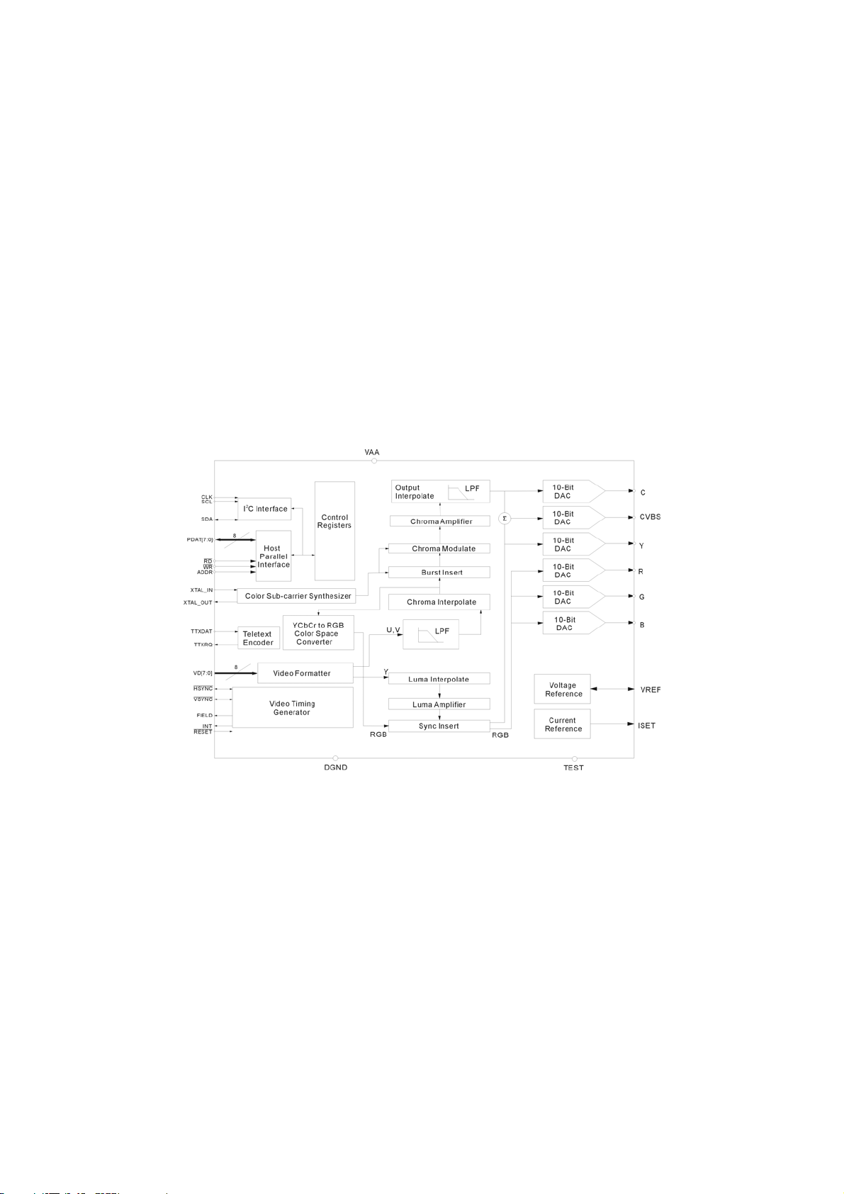
2-1-2 NTSC/PAL Digital Video Encoder (CS4955)
FEATURES
• Six DACs providing simultaneous composite, S-video,
and RGB or Component YUV outputs
• Programmable DAC output currents for low
imped-ance(37.5Ω) and high impedance(150
Ω)loads.
• Multi-standard support for NTSC-M, NTSC-JAPAN,
PAL (B, D, G, H, I, M, N, Combination N)
• ITU R.BT656 input mode supporting EAV/SAV codes
and CCIR601 Master/Slave input modes
• Porgrammable HSYNC and VSYNC timing
• Multistandard Teletext(Europe, NABTS, WST)
support
• VBI encoding support
• Wide-Screen Signaling (WSS) support,
EIA-JCPX1204)
• NTSC closed caption encoder with interrupt
• CS4955 supports Macrovision copy protection
Version 7
2
• Host interface configurable for parallel or I
C
compatible operation
• On-chip voltage reference generator
• +.3.3V or +5V operation, CMOS, low-power modes,
tri-state DACs
Ordering Information
CS4955-CQ 48-pin TQFP
DESCRIPTION
The CS4955 provides full conversion from digital video formats YcbCr or YUV into NTSC and PAL Composite,
Y/C (S-video) and RGB, or YUV analog video. Input formats can be 27MHz 8-bit YUV, 8-bit YcbCr, or
ITUR.BT656 with support for EAV/SAV codes. Video output can be formatted to be compatible with NTSC-M,
NTSC-J, PAL-B, D, G, H, I, M, N, and Combination N systems. Closed Caption is supported in NTSC. Teletext is
supported for NTSC and PAL.
Six 10-bit DACs provide two channels for an S-Video output port, one or two composite video outputs, and three
RGB or YUV outputs. Two-times oversampling reduces the output filter requirements and guarantees no DAC-ralated
modulation components within the specified bandwidth of any of the supported video standards.
Parallel or high-speed I
parallel interface doubles as a general purpose I/O port when the CS4954 is in I
board area.
6
2
C compatible conpatible control interfaces are provided for flexibility in system design. The
2
C mode to help conserve valuable
Page 9
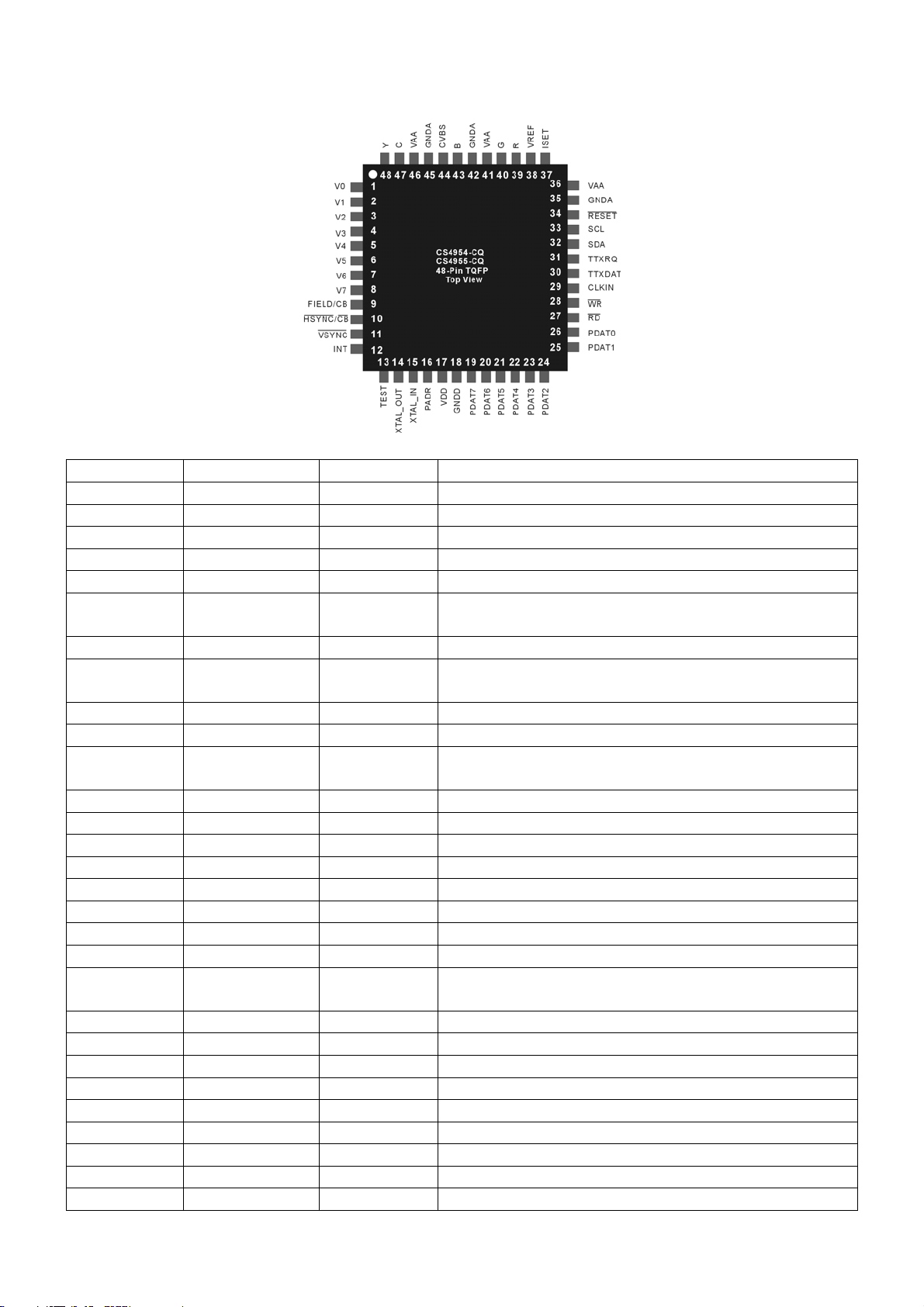
PIN DESCRIPTIONS
Pin Name Pin Number Type Description
V[7:0] 8,7,6,5,4,3,2,1 IN Digital video data inputs
CLK 29 IN 27MHz input clock
PADDR 16 IN Address enable line
XTAL_IN 15 IN Subcarrier crystal input
XTAL_OUT 14 OUT Subcarrier crystal input
HSYNC/CB 10 I/O Active low horizontal sync, or composite blank
signal
VSYNC 11 I/O Active low vertical sync
FIELD/CB 9 OUT Video field ID. Selectable polarity or composite
blank
RD 27 IN Host parallel port read strobe, active low
WR 28 IN Host parallel port write strobe, active low
PDAT[7:0] 19,20,21,22,23,
I/O Host parallel port/general purpose I/O
24,25,26
SDA 32 I/O I2C data
SCL 33 IN I2C clock input
CVBS 44 CURRENT Composite video output
Y 48 CURRENT Luminance analog output
C 47 CURRENT Chrominance analog output
R 39 CURRENT Red analog output
G 40 CURRENT Green analog output
B 43 CURRENT Blue analog output
VREF 38 I/O Internal voltage reference output or external
reference input
ISET 37 CURRENT DAC current set
TTXDAT 30 IN Teletext data input
TTXRQ 31 OUT Teletext request output
INT 12 OUT Interrupt output, active high
RESET 34 IN Active low master RESET
TEST 13 IN TEST pin. Ground for normal operation
VAA 36,41,46 PS +5V or +3.3V supply(must be same as VDD)
GNDD 18 PS Ground
VDD 17 PS +5V or 3.3V supply (must be same as VAA)
7
Page 10

GNDA 35,42,45 PS Ground
2-1-3 DVD Processor Chip (MTK1369AE)
* Features
z Single-chip DVD video decoder in a 208-pin PQFP package
z Supports MPEG-1 system and MPEG-2 program streams
z Programmable multimedia processor architecture
z Compatible with Audio CD, Video CD, VCD 3.0, and Super Video CD (SVCD)
z DVD Navigation 1
z Built-in content Scrambling System (CSS)
- Audio
z Built-in Karaoke key-shift functio n
z DolbyTM Digital 2-channel down mix audio output for DolbyTM
z Dolby Pro Logic
z Linear PCM streams for24 bit / 96KHz
z Concurrent S/PDIF out and 2-channel audio output
z Sensaura Dolby Digital Virtual Surround
z DTS Digital Surround 2-channel down mix stereo output
z S/PDIF output for encoded AC-3, DTS Digital output or Linear PCM
- Peripheral
z Glueless interface to DVD loaders (ATAPI or A/V bus I/F)
z Bi-directional 12C audio interface
z 8 general-purpose auxiliary ports
z Single 27MHz clock input
- Smart Technology
z SmartZoomTM for motion zoom & pan
z SmartZoomTM for NTSC to PAL conversion and vice versa
SmartZoomTM for video error concealment
z
* Functional Description
8
Page 11
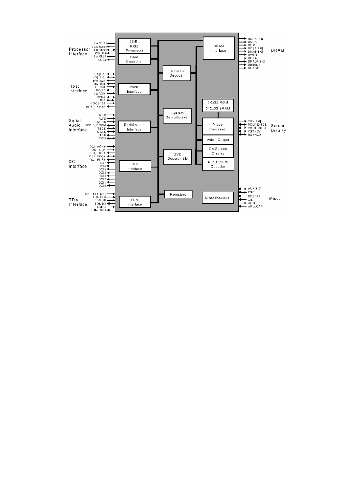
* Pinout Diagram
9
Page 12

10
Page 13

PIN DESCRIPTON
PIN Symbol Type Description
1 IREF Analog Input
2 PLLVSS Ground Ground for data PLL and related analog circuitry
3 LPIOP Analog output Positive output of the low pass filter
4 LPION Analog output Negative output of the low pass filter
5 LPFON Analog output Negative output of loop filter amplifiter
6 LPFIP Analog input Positive input of loop filter amplifier
7 LPFIN Analog input Negative input of loop filter amplifier
8 LPFOP Analog output Positive output of loop filter amplifier
9 JITFO Analog output RF jitter meter output
10 JITFN Analog input Negative input of the operation amplifier for RF jigger meter
11 PLLVDD3 Power Power for data PLL and related analog circuitry
12 FOO Analog output Focus servo output. PDM output of focus servo compensator
13 TRO Analog output Tracking servo output.PDM output of tracking servo compensator
14 TROPENPWM Analog outpu
15 PWMOUT2 Analog outpu The general PWM output
16 DVDD2 Power 2.5V power
17 DMO Analog outpu Disk motor control output.PWM output
18 FMO Analog outpu Feed motor control. PWM output
19 FG Inout, pull up Motor Hall sensor input
20 DVSS Ground Ground
21 HIGHA0 Inout, pull up Microcontroller address 8
22 HIGHA1 Inout, pull up Microcontroller address 9
23 HIGHA2 Inout, pull up Microcontroller address 10
24 HIGHA3 Inout, pull up Microcontroller address 11
25 HIGHA4 Inout, pull up Microcontroller address 12
26 HIGHA5 Inout, pull up Microcontroller address 13
27 DVSS Ground Ground
28 HIGHA6 Inout, pull up Microcontroller address 14
29 HIGHA7 Inout, pull up Microcontroller address 15
30 AD7 Inout Microcontroller address/data 7
31 AD6 Inout Microcontroller address/data 6
32 AD5 Inout Microcontroller address/data 5
33 AD4 Inout Microcontroller address/data 4
34 DVDD3 Power 3.3V power
35 AD3 Inout Microcontroller address/data 3
36 AD2 Inout Microcontroller address/data 2
37 AD1 Inout Microcontroller address/data 1
38 AD0 Inout Microcontroller address/data 0
39 IOA0 Inout, pull up Microcontroller address 0/GPIO0
40 IOA1 Inout, pull up Microcontroller address 0/GPIO1
41 DVDD2 Power 2.5V power
42 IOA2 Inout, pull up Microcontroller address 0/GPIO2
43 IOA3 Inout, pull up Microcontroller address 0/GPIO3
44 IOA4 Inout, pull up Microcontroller address 0/GPIO4
45 IOA5 Inout, pull up Microcontroller address 0/GPIO5
46 IOA6 Inout, pull up Microcontroller address 0/GPIO6
47 IOA7 Inout, pull up Microcontroller address 0/GPIO7
48 A16 Outpu Flash address 16
49 A17 Output Flash address 17
50 IOA18 Inout Flash address 18 / GPIO10
51 IOA19 Inout Flash address 19 / GPIO11
52 DMVSS Ground Ground for DRAM clock circuitry
53 DMVDD3 Power Power for DRAM clock circuitry
Current reference input.it generate reference current for data PLL
Connect an external 100K resistor to this pin and PLLVSS.
Tray open output,co nt r ol l ed b y m i croco ntroller.
This is PWM output for TRWMEN
TRWMEN
27Hrw2=0
27hRW2=1 or is digital output for
11
Page 14

PIN Symbol Type Description
54 ALE Inout,pull up Microcontroller address latch enable
55 IOOE# Inout Flash output enab le,active low /GPIO13
56 IOWR# Inout Flash write enable,active low /GPIO17
57 IOCS# Inout,pull up Flash chip select,active low /GPIO18
58 DVSS Ground Ground
59 UP1_2 Inout,pull up Microcontroller port 1-2
60 UP1_3 Inout,pull up Microcontroller port 1-3
61 UP1_4 Inout,pull up Microcontroller port 1-4
62 UP1_5 Inout,pull up Microcontroller port 1-5
63 UP1_6 Inout,pull up Microcontroller port 1-6
64 DVDD3 Power 3.3V power
65 UP1_7 Inout,pull up Microcontroller port 1-7
66 UP3_0 Inout,pull up Microcontroller port 3-0
67 UP3_1 Inout,pull up Microcontroller port 3-1
68 INT0# Inout,pull up Microcontroller in terrupt 0,active low
69 IR Input IR control signal input
70 DVDD2 Power 2.5V power
71 UP1_4 Inout Microcontroller port 3-4
72 UP1_5 Inout Microcontroller port 3-5
73 UWR# Inout,pull up Microcontroller write strobe,active low
74 URD# Inout,pull up Microcontroller read strobe,active low
75 XTALI Input Crystal input,27MHz
76 XTALO Output Crystal output
77 DVSS Ground Ground
78 RD7 Inout DRAM data 7
79 RD6 Inout DRAM data 6
80 RD5 Inout DRAM data 5
81 RD4 Inout DRAM data 4
82 DVDD2 Power 2.5V power
83 RD3 Inout DRAM data 3
84 RD2 Inout DRAM data 2
85 RD1 Inout DRAM data 1
86 RD0 Inout DRAM data 0
87 RWE# Output DRAM write enable,active low
88 CAS# Output DRAM column address strobe,active low
89 RAS# Output DRAM row address strobe,active low
90 RCS# Output DRAM chip select,active low
91 BA0 Output DRAM bank address 0
92 DVDD3 Power 3.3V power
93 RD15 Inout,pull up/down DRAM data 15
94 RD14 Inout,pull up/down DRAM data 14
95 RD13 Inout,pull up/down DRAM data 13
96 RD12 Inout,pull up/down DRAM data 12
97 DVSS Ground Ground
98 RD11 Inout,pull up/down DRAM data 1 1
99 RD10 Inout,pull up/down DRAM data 10
100 RD9 Inout,pull up/down DRAM data 9
101 RD8 Inout,pull up/down DRAM data 8
102 VPVDD3 Power Power for varipitch VCO circuitry
103 VCOCIN Analog input Connect capacitor for compensator loop filter
104 VPVSS Ground Ground for varipitch VCO circuitry
105 DVSS Ground Ground
106 CLK Output DRAM clock
107 CLE Output DRAM clock enable
108 RA11 Output DRAM address bit 11 or audio serial data 3 (channel 7/8)
109 RA9 Output DRAM address 9
110 RA8 Output DRAM address 8
111 DVDD2 Power 2.5V power
112 RA7 Output DRAM address 7
12
Page 15

PIN Symbol Type Description
113 RA6 Output DRAM address 6
114 RA5 Output DRAM address 5
115 RA4 Output DRAM address 4
116 DVSS Ground Ground
117 DQM1 Output Mask for DRAM input/output byte 1
118 DQM0 Output Mask for DRAM input/output byte 0
119 BA1 Output DRAM bank address 0
120 RA10 Output DRAM address 10
121 DVDD2 Power 2.5V power
122 RA0 Output DRAM address 0
123 RA1 Output DRAM address 1
124 RA2 Output DRAM address 2
125 RA3 Output DRAM address 3
126 DVSS Ground Ground
127 RD31 Inout,pull up/down DRAM data 31
128 RD30 Inout,pull up/down DRAM data 30
129 RD30 Inout,pull up/down DRAM data 29
130 RD29 Inout,pull up/down DRAM data 28
131 DVDD3 Power 3.3V power
132 RD27 Inout,pull up/down DRAM data 27
133 RD26 Inout,pull up/down DRAM data 26
134 RD25 Inout,pull up/down DRAM data 25
135 RD24 Inout,pull up/down DRAM data 24
136 DVSS Ground Ground
137 DQM3 Output Mask for DRAM input/output byte 3
138 DQM2 Output Mask for DRAM input/output byte 2
139 RD23 Inout,pull up/down DRAM data 23
140 RD22 Inout,pull up/down DRAM data 22
141 DVDD2 Power 2.5V power
142 RD21 Inout,pull up/down DRAM data 21
143 RD20 Inout,pull up/down DRAM data 20
144 RD19 Inout,pull up/down DRAM data 19
145 RD18 Inout,pull up/down DRAM data 18
146 DVSS Ground Ground
147 RD17 Inout,pull up/down DRAM data 17
148 RD16 Inout,pull up/down DRAM data 16
149 ABCK Output Audio bit clock
150 ALRCK Input,pull down
151 DVDD3 Power 3.3V power
152 ASDATA0 Input,pull down Audio serial data 0 (left/right channel)
153 ASDATA1 Input,pull down Audio serial data 1 (surround left/surround right channel)
154 ASDATA2 Input,pull down Audio serial data 2 (center/LFE channel)
155 ACLK Inout Audio DAC master clock (384/256 audio sample frequency)
156 APVDD3 Power Power for audio clock circuitry
157 APVSS Ground Ground for audio clock circuitry
158 SPDIF Output SPDIF output
159 MC_DAT Input Microphone serial input
160 BLANK# Inout Video blank area, active low / GPIO14
161 VSYN Inout Vertical sync / GPIO16
162 HSYN Inout Horizontal sync / GPIO15
163 DVSS Ground Ground
164 YUVO Output Video data output bit 0
165 YUV1 Output Video data output bit 1
166 YUV2 Output Video data output bit 2
167 YUV3 Output Video data output bit 3
168 YUV4 Output Video data output bit 4
169 DVDD2 Power 2.5V power
170 YUV5 Output Video data output bit 5
171 YUV6 Output Video data output bit 6
(1) Audio left/right channel clock (2)Trap value in power-on reset.
1:use external 373, 0:use internal 373
13
Page 16

PIN Symbol Type Description
172 YUV7 Output Video data output bit 7
173 ICE Input,pull down Microcontroller ICE mode enable
174 PRST Input,pull down Pow e r on reset input, active high
175 DVSS Ground Ground
176 VFO13 Output The 1st, 3rd VFO pulse output of DVD-R AM ID header
177 IDGATE Output DVD-RAM ID header detect signal output
178 DVDD3 Power 3.3V power
179 UDGATE Output DVD-RAM recording data gate signal o ut p ut
180 WOBSI Input Wobble signal input
181 SDATA Output RF serial data input
182 SDEN Output RF serial data latch enable
183 SLCK Output RF serial clock output
184 BDO Input,pull down Flag of defect data status input
185 DVDD3 Power 3.3V power
186 PDMVDD3 Power Power for PDM circuitry
187 PWMVREF Analog input A reference voltage input for PWM circuitry.A typical value of 2.8v
188 PWM2VREF Analog input A reference voltage input for PWM circuitry.A typical value of 1.4v
189 PDMVSS Ground Ground for PDM circuitry
190 ADCVSS Ground Ground for ADC circuitry
191 ADIN Analog input General A/D input
192 RFSUBI Analog input RF subtraction signal input terminal
193 TEZISLV Analog input Tracking error zero crossing low pass input
194 TEI Analog input Tracking error input
195 CSO Analog input Central servo input
196 FEI Analog input Focus error input
197 RFLEVEL Analog input Sub beam add input or RFRP low pass input
198 RFRP_DC Analog input RF ripple detect input
199 RFRP_AC Analog input RF ripple detect input (through AC coupling)
200 RFRPSLV Analog input RFRP slice level input
201 HRFZC Analog input High frequency RF ripple zero crossing
202 ADCVDDS Power Power for ADC circuitry
203 RFDTSLVP Analog output Positive RF data slicer level output
204 SCON Analog output Negative analog slicer current output
205 SCOP Analog output Positive analog slicer current output
206 RFDTSLVN Analog output Negative RF data slicer level output
207 RFIN Analog input Negative input of RF differential signal
208 RFIP Analog input Positive input of RF differential signal
MT1336
GENERAL DESCRIPTION
MT1336 is a high performance CMOS analog front-end IC for both CD_ROM driver up to 48xs and DVD-ROM driver up
to 16xs. It also supports DVD-RAM read up to 4xs Version 2. It contains servo amplifiers to generate focusing error,
3-beam tracking error, 1 beam radial push-pull signal, RF level and SBAD for servo functions. It also includes DPD
tracking error signal for DVD_ROM application. For DVD-RAM disks, there are also Differential Push-Pull (DPP) method
for generating tracking signal and Differential Astigmatic Detection (DAD) for processing focusing signal. Programmable
equalizer and AGC circuits are also incorporated in this chip to optimize read channel performance. In addition, this chip
has dual automatic laser power control circuits for DVD-ROM (DVD-RAM) and CD-ROM seperately and reference
voltage generators to reduce external components. Programmable functions are implemented by the access of internal
register through bi-directional serial port to configure modes selection.
FEATURES
. RF equalizer with programmable f
. MT1336 supports at least eight different kinds of pick-up heads with versatile input configuration for both RF input stages
and servo signal blocks.
from 3MHz to 70MHz and programmable boost from 3db to 13db.
c
14
Page 17

. Versatile on-line AGC.
. 3 beams tracking error signal generator for CD_ROM application.
. One beam differential phase tracking error (DPD) generator for DVD_ROM application.
. Differential push pull tracking error (DPP) generator for DVD_RAM application.
. Focusing error signal generator for CD-ROM, DVD-ROM and DVD-RAM (DAD method).
. RF level signal generator.
. Sub-beam added signal for 3 beams CD_ROM.
. One beam push-pull signal generator for central servo application.
. High speed RF envelop detection circuit with bandwidth up to 400KHz for CD-ROM.
. Defect and Blank detection circuits
. Dual automatic laser power control circuits with programmable level of LD monitor voltage.
. Vref-1.4V voltage and V2ref=2.8V voltage generators.
. V20=2.0V voltage for pick - up head refe rence.
. Bi-directional serial port to access internal registers.
. 128-pin LQFP
Block Diagram…………………………………..P.3
Pin Assignment and Description………………..P.4-9
Functions
1.) RF Path Description………………….P. 10-13
2.) Servo Signal…………………………..P. 14-17
. Focusing Error
. Central Servo
. Tracking Error
. RFLVL & SBAD (LVL)
3.) ALPC & RFRP ( RF Ripple)………….P. 18
4.) WOBBLE Detection…………………..P. 19
Command Access Timings………………………P. 20
Programmable I/O ………………………………P. 21
Register
1.) Register Map………………………….P. 22-24
2.) Register Description………………….P . 25-50
MT1336 PIN DESCRIPTIONS
Pin Numbers Symbol Type Description
LQFP128
RF Flag interface
23 DEFECT Digital input Flag of bad data output status
RF SIO interface
56 SCLK Digital input RF serial clock input
58 SDEN Digital inpu t RF serial data enable
59 SDATA Digital IO RF serial data IO
60 RST Digital input Reset (active high)
55 XCK16M Digital input 16.9MHz for verification
RF SERVO interface
40 UDGATE Digital input Control signal for DVD-RAM
41 IDGATE Digital input Control signal for DVD-RAM
38 VFO13 Digital input DVD-RAM Header signal
RF
15
Page 18

100 DVDA Analog input AC coupled DVD RF signal input A
99 DVDB Analog input AC coupled DVD RF signal input B
98 DVDC Analog input AC coupled DVD RF signal input C
97 DVDD Analog input AC coupled DVD RF signal input D
95 DVDRFIN Analog input AC coupled DVD RF signal input RFIN
96 DVDRFIP Analog input AC coupled DVD RF signal input RFIP
94 CDA Analog input AC coupled CD RF signal input A
93 CDB Analog input AC coupled CD RF signal input B
92 CDC Analog input AC coupled CD RF signal input C
91 CDD Analog input AC coupled CD RF signal input D
90 OSN Analog RF Offset cancellation capacitor connection
89 OSP Analog RF Offset cancellation capacitor connection
85 CEQP Analog RF Offset cancellation capacitor connection
84 CEQN Analog RF Offset cancellation capacitor connection
88 RFGC Analog RF AGC loop capacitor connecting for DVD-ROM
87 RFGCU Analog RF AGC loop capacitor connecting for DVD-ROM
86 RFGCI Analog RF AGC loop capacitor connecting for DVD-ROM
101 MA Analog input DC coupled DVD-RAM main-beam RF signal input A
102 MB Analog input DC coupled DVD-RAM main-beam RF signal input B
103 MC Analog input DC coupled DVD-RAM main-beam RF signal input C
104 MD Analog input DC coupled DVD-RAM main-beam RF signal input D
105 SA Analog input DC coupled DVD-RAM sub-beam RF signal input A
106 SB Analog input DC coupled DVD-RAM sub-beam RF signal input B
110 SC Analog input DC coupled DVD-RAM sub-beam RF signal input C
111 SD Analog input DC coupled DVD-RAM sub-beam RF signal input D
108 IR Analog External current bias resistor (R=20K)
119 AGC1 Analog Wobble AGC loop1 capacitor
121 AGC2 Analog Wobble AGC loop2 capacitor
122 AGC3 Analog Wobble AGC loop3 capacitor
127 RFSUBO Analog output Header push-pull RF output signal
1 WOBSO Analog output Wobble signal output
6 RFOP Analog output RF positive output
7 RFON Analog output RF negative output
TRACKING ERROR
32 DPFN Analog DPD amplifier negative input
33 DPFO Analog DPD amplifier output
61 DPDMUTE Digital input DPD mute control input
116 TNI Analog input 3 beam satellite PD signal negative input
115 TPI Analog input 3 beam satellite PD signal positive input
21 TEO Analog Output Tracking error output
FOCUSING ERROR & RF LEVEL & CENTRAL SERVO SIGNAL
112 CDFOP Analog input CD focusing error positive input
113 CDFON Analog input CD focusing error negative input
18 FEO Analog output Focusing error output
19 LVL Analog output RF level output
20 CSO Analog output Central servo signal output
ALPC
124 MDI1 Analog input Laser power monitor input
125 LDO1 Analog Output Laser driver output
123 MDI2 Analog input Laser power monitor input
126 LDO2 Analog Output Laser driver output
RF RIPPLE
26 CRTP Analog RF top envelop filter capacitor connecting
27 CRTPLP Analog Defect level filter capacitor connecting
25 HRFRP Analog output High frequency RF ripple output or Blank detector’s output
24 LRFRP Analog output Low frequency RF ripple output
POWER
67,69 AVDD Power Master PLL Filter power
65,73 AGND GND GND for Master PLL Filter
64 AVDD Power DPD Power
62 AGND GND DPD GND
16
Page 19

109 AVDD Power RF path Power
107 AGND GND RF path GND
114 SVDD Power Servo Power
117 SGND GND Servo GND
2,120 WAVDD Power Wobble Power
128,118 WAGND GND Wobble GND
5 AVDDO Power Power for RF output
8 AGNDO GND GND for RF output
14 AVDDT Power Power for trimming PAD
12 AGNDT GND GND for trimming PAD
22 VDDP Power Peak Detection Power
31 GNDP GND Peak Detection GND
37,54 VDD Power Serial I/O Power
39,57 GND GND Serial I/O GND
REFERENCE VOLTAGE
16 VREFO Analog output Reference voltage 1.4V
15 V2REFO Analog output Reference voltage 2.8V
17 V20 Analog output Reference voltage 2.0V
ALPC TRIMMING
9 TM1 Analog input Trimming pin for ALPC1
10 TM2 Analog input Trimming pin for ALPC1
11 TM3 Analog input Trimming pin for ALPC2
13 TM4 Analog input Trimming pin for ALPC2
HIGH SPEED TRACK COUNTING
29 TRLP Analog Low-pass filter capacitor connecting
28 TRLPA Analog Low-pass filter capacitor connecting
30 HTRC Digital output High speed track counting digital output
PCS
74 HALLSIN Analog input Negative input of amplifier for hall sensor signal
75 REFSIN Analog input Positive input of amplifier for hall sensor signal
76 SINPHI Analog output Amplifier output for hall sensor signal
71 HALLCOS Analog input Negative input of amplifier for hall sensor signal
72 REFCOS Analog input Positive input of amplifier for hall sensor signal
70 COSPHI Analog output Amplifier output for hall sensor signal
FOR MONITOR ONLY
81 MON Analog output
80 MOP Analog output
66 VCON Analog output
77 SWO Analog output Output from mux of SW1 & SW2
78 SW2 Analog input External input for servo input select
79 SW1 Analog input External input for servo input select
FOR SERIAL I/O
42 IO0
43 IO1
44 IO2
45 IO3
46 IO4
47 IO5
48 IO6
49 IO7
50 IO8
51 IO9
52 IOA
53 IOB
2-1-4 20-Pin, 24-Bit, 96kHz Stereo D/A with Volume Control (WM8720)
Features
♦ Performance:
-102dB SNR (‘A’ weighted @48kHz),
-THD: -95dB @ 0dB FS
♦ 5V or 3.3V supply operation
♦ Sampling frequency: 8kHz to 96kHz
17
Page 20

♦ Input data word: 16 to 24-bit
♦ Hardware or SPI compatible serial port control
modes:
-Hardware mode:system clock, reset, mute,
de-emphasis
-Serial control mode: mute, de-emphasis, digital
attenuation(256 steps), zero mute, phase
reversal, power down
♦ Compatible with PCM1720
Description
The WM820 is a high performance stereo DAC
designed for audio applications such as CD, DVD,
home theatre systems, set top boxes and digital TV.
The WM8720 supports data input word lengths from
16 to 24-bits and sampling rates up to 96kHz. The
WM8720 consists of a serial interface port, digital
interpolation filter, multi-bit sigma delta modulator and
stereo DAC in a small 20-pin SSOP package. The
WM8720 also includes a digitally controllable mute
and attenuator function on each channel.
The WM8720 supports a variety of connection
schemes for audio DAC control. The SPI-compatible
serial control port provides access to a wide range of
features including on-chip mute, attenuation and
phase reversal. A hardware controlllable interface is
also available.
The programmable data input port supports a variety
of glueless interfaces to popular DSPs, audio
decoders and S/PDIF and AES/EBU receivers.
APPLICATIONS
. CD, DVD audio
. Home theare systems
. Set top boxes
. Digital TV
18
Page 21

BLOCK DIAGRAM
PIN DESCRIPTIONS
PIN NAME TYPE DESCRIPTION
1 PWDN Digital input Powerdown control; low is ON, high is POWER OFF, Interal pull-down.
2 SCKI Digital input System clock input(256 or 384fs).
3 TEST Digital output Reserved.
4 ML/I2S Digital input Latch enable (software mode) or input format selection (hardware mode)
Internal pull-up.
5 MC/IWL Digital input Serial control data clock input (software mode) or input word length
selection (hardware mode). Internal pull-up.
6 MD/DM Digital input Serial control data input (software mode) or de-emphasis selection
(hareware mode). Internal pull-up.
7 RSTB Digital input Reset input-active low. Internal pull-up.
8 ZERO Digital output Infinite zero detect-active low. Open drain type output with active
pull-down.
9 VOUTR Analogue output Right channel DAC output.
10 AGND Supply Analogue ground supply.
11 AVDD Supply Analogue positive supply.
12 VOUTL Analogue output Left channel DAC output.
13 CAP Analogue output Analogue internal reference.
14 BCKIN Digital input Audio data bit
15 DIN Digital input Serial audio data input.
16 LRCIN Digital input Sample rate clock input.
17 MUTE Digital IO Mute control pin, input or automute output.
Low is not mute, high is mute, Z is automute.
18 MODE Digital input Mode select pin. Low is software mode, high is hardware control.
Internal pull-down.
19 DVDD Supply Digital positive supply.
20 DGND Supply Digital ground supply.
Note:
19
Page 22

Digital input pins have Schmitt trigger input buffers.
2-1-5 Serial EEPROM, 2K (256 x 8) (24C16)
* Features
z Low-Voltage and Standard-Voltage Operation
-5.0 (V CC = 4.5V to 5.5V)
-2.7 (V CC = 2.7V to 5.5V)
-2.5 (V CC = 2.5V to 5.5V)
-1.8 (V CC = 1.8V to 5.5V)
z Internally Organized 128 x 8 (1K), 256 x 8 (2K), 512 x 8 (4 K) , 10 2 4 x 8 (8 K) or 2048 x 8 (16K)
z 2-Wire Serial Interface
z Schmitt Trigger, Filtered Inputs for Noise Suppression
z Bi-directional Data Transfer Protocol
z 100 kHz (1.8v, 2.5V, 2.7V) and 400 kHz (5V) Compatibility
z Write Protect Pin for Hardware Data Protection
z 8-Byte Page (1K, 2K), 16-Byte Page (4K, 8K, 16K) Write Modes
z Partial Page Writes Are Allowed
z Self-Timed Write Cycle (10 ms max)
z High Reliability
- Endurance: 1 Million Write Cycles
- Data Retention: 100 Years
- ESD Protection: >3000V
z Automotive Grade and Extended Temperature Devices Available
z 8-Pin and 14-Pin JEDEC SOIC, 8-Pin PDIP, 8-Pin MSOP, and 8-Pin TSSOP Packages
* Pin Configurations
* Pin Description
Pin Name Function
A0-A2 Address Inputs
SDA Serial Data
SCL Serial Clock input
WP Write Protect
NC No Connect
2-1-6 8M-BIT [1Mx8/512Kx16] CMOS FLASH MEMORY
FEATURES
• 1,048,576 x 8/524,288 x 16 switchable
• Single power supply operation
- 5.0V only operation for read, erase and program
20
Page 23

operation
• Fast access time: 70/90/120ns
• Low power consumption
- 50mA maximum active current
- 0.2uA typical standby current
• Command register architecture
- Byte/word Programming (7us/12us typical)
- Sector Erase (Sector structure 16K-Bytex1,
8K-Bytex2, 32K-Bytex1, and 64K-Byte x15)
• Auto Erase (chip & sector) and Auto Program
- Automatically erase any combination of sectors with
Erase Suspend capability.
- Automatically program and verify data at specified
address
• Erase suspend/Erase Resume
- Suspends sector erase operation to read data from,
or program data to, another sector that is not being
erased, then resumes the erase.
• Status Reply
- Data polling & Toggle bit for detection of program and
erase operation completion.
• Ready/Busy pin (RY/BY)
- Provides a hardware method of detecting program
or erase operation completion.
• Sector protection
- Sector protect/chip unprotect for 5V/12V system.
- Hardware method to disable any combination of
sectors from program or erase operations
- Tempory sector unprotect allows code changes in
previously locked sectors.
• 100,000 minimum erase/program cycles
• Latch-up protected to 100mA from -1V to VCC+1V
• Boot Code Sector Architecture
- T = Top Boot Sector
- B = Bottom Boot Sector
• Low VCC write inhibit is equal to or less than 3.2V
• Package type:
- 44-pin SOP
- 48-pin TSOP
• Compatibility with JEDEC standard
- Pinout and software compatible with single-power
supply Flash
21
Page 24

22
Page 25

2-1-7 512K X 16 Bit X 2 Banks Synchronous DRAM (A43L0616)
Features
JEDEC standard 3.3V power supply
LVTTL compatible with multiplexed address
Dual banks / Pulse RAS
MRS cycle with address key programs
- CAS Latency (2,3)
- Burst Length (1,2,4 ,8 & full page)
- Burst Type (Sequential & interleave)
All inputs are sampled at the positive going edge of the system clock
Burst Read Single-bit Write operation
DQM for masking
Auto & self refresh
64ms refresh period (4K cycle)
50 Pin TSOP (II)
Pin Configuration
23
Page 26

24
Page 27

Block Diagram
Pin Descriptions
Symbol Name Description
CLk System Clock Active on the positive going edge to sample all inputs
CS Chip Select Disables or Enables device operation by masking or enabling
all inputs except CLK, CKE and L(U)DQM
Masks system clock to freeze operation from the next clock cycle.
CKE Clock Enable CKE should be enabled at least one clock + tss prior to new command.
Disable input buffers for power down in standby.
A0~A10/AP Address
Row/Column addresses are multiplexed on the same pins.
Row address: RA0 ~ RA10, Column address: CA0 ~ CA7
BA Bank Select Address
Selects bank to be activated during row address latch time.
Selects band for read/write during column address latch time.
RAS Row address Strobe
Latches row addresses on the positive going edge of the CLK with
RAS low.
Enables row access & precharge.
CAS
Column Address Strobe
Latches column addresses on the positive going edge of the CLK with CAS
low. Enables column access.
WE Write Enable Enables write operation and Row precharge.
25
Page 28

Symbol Name Description
L(U)DQM
DW0-15 Data Input/Output Data inputs/outputs are multiplexed on the same pins .
VDD/VSS Power Supply/Ground Power Supply: +3.3V±0.3V/Ground
VDDQ/VSSQ
NC/RFU No Connection
Data Input/Output Mask
Data Output
Power/Ground
Makes data output Hi-Z, t SHZ after the clock and masks the output.
Blocks data input when L(U)DQM active.
Provide isolated Power/Ground to DQs for improved noise immunity.
3. Product Specifications
Playback System
DVD Vi deo
Video CD (1.1, 2.0, 3.0)
SVCD and CVD
CDDA
CD-ROM with MP3 data
PICTURE CD
Television Signal System
NTSC/PAL
Video Performance
Video Out 1 Vpp into 75 ohm
S-Vi deo Out Y: 1Vpp into 75 ohm
C: 0.286 Vpp into 75 ohm
D/A Converter 27MHz/10bit
Audio Performance
Frequency Response DVD: fs 48/96KHz, 4Hz~22/44K Hz
Video CD: fs 44.1KHz, 4Hz~20KHz
Audio CD: fs 44.1KHz, 4Hz~20KHz
Output Level Analog: 2Vrms(1KHZ)
Digital: 1.15 Vpp
D/A Converter 96KHz/24bit
S/N Ratio 90dB
Connections
Coaxial digital out X1
Audio Analog out for 2-channel X1
S-Vi deo out X1
Power Supply
Power Source AC100~255V, 50/60Hz
Power Consumption <25 Watt
Set
Dimensions (W X H X D) 430 X 52 X 295 (mm)
Net W ei ght 2.6 Kg
Gross Weight 4.0 Kg
26
Page 29

5. Disassembly and Reassembly
27
Page 30

6. T roubleshooting
N
No power Insert the AC power plug securely into the power outlet.
Make sure that the equipment is connected properly.
No picture
No sound Make sure that the equipment is connected properly.
Distorted sound
No fast forward or fast reverse Some discs may have sections that prohibit fast forward or fast reverse.
No proper aspect ratio Select the correct setup for TV aspect ratio that matches your TV set.
o operations can be performed with
the remote controller
No button operation
Audio soundtrack and/or Subtitle
language is not the one you selected.
No Angle change
Make sure that the input setting for TV is Video (AV).
Make sure that the input settings for the TV and stereo system are correct.
Check the batteries are installed with the correct polarities.
Point the remote control unit at the remote control sensor and operate.
Remove the obstacles between the remote control unit and remote control
sensor.
Set the POWER button to OFF and then back to ON.
Alternatively, turn off the power, disconnect the power plug and then
reconnect it.
If the audio soundtrack and /or subtitle language does not exist on the
disc, the language selected at the initial settings will not be seen.
This function is dependent on software availability. Even if a disc has a
number of angles recorded, these angles may be recorded for specific
scenes only .
28
Page 31

p
7. Electrical Part List CO-01 PRODUCT DESIGN PACKAGE LIST
No. Name Counts Blueprint No. Material No. Notes
1 CO-01 surface subassembly 1
2 SANYO HD60 loader 1
Two-channel decoding sub-
4
assembly for CO-01 DVD
5 CO-DPA118 subassembly 1 CO-DPA118
6 Interface subassembly of SCART 1
7 CO-01 motherboard 1 CO-DZCO-01 silver-gray, use electrolyzed iron
8 CO-01 backboard 1 CO-01HB silk-screen file No.: CO9
ower supply switch 1 PS8-4 6A 250V AC 10A 125V AC
10 pyrocondensation conducting tube
11 outer cover 1 CO-01WZ with mark of DECCAVIDEO
1 CO-DJA1369XE+SANYO with microphone and s-video output
12 wire of power-supply 1 black,two round-heads, ,with VDE certification
13 PE bag for power-supply wire 1
14 nylon-ribbon fastening string 5
15 black fastening string 1 for power-supply wire
17 CO-01 CD gate-bar 1 CO-01CDM for SANYO HD60 loader
18 sticker for DVD trademark 1 with background black and characters silvery
19 strut for circuit board 8
21 plastic nut cap 8
unit80*160mm with mark of
environment-protecting
2 for decodeing board6 for power-supply
board
decodeing board 4power-supply board 6
29
Page 32

No. Name Counts Blueprint No. Material No. Notes
r
p
p
22
rubber mat
23 VCD rubber mat 3
2
thickness 2mm diameter 12mm
thickness 19.5mmdiameter 9.5mm
24 Remote controller-V1 1
25 battery 2
26 PE bag for remote controller 1
7# environment-protecting battery
ENGLISH
Unit: 05*80*260mm with
environment-protecting mark
27 manual 1
28 PE bag for manual 1
English
unit: 05*80*260mm with
environment-protecting mark
29 foam 1 CO-108PM 355*110*80
30 handle for colourbox 1
31 colourbox 1
32 pearl cotton 480*580 1
Unit: mm with environment-protecting mark
33 nail BTV3*10 colouful zinc 4 4 for loader
with-cap hardened nailBTPW3*8
34
colorful zinc
8
4 for outer cover4 for loader
round-headed self-fastened
35
hardened nailBTV3*6 colorful
zinc
14
3 for backboard, 4 for outer cover, 2 for side
cover, 3 for cover and motherboard, 2 fo
shielding
round-headed self-fastened
36
hardened nailBTV3*16
8
ower-supply board: 6decoding board: 2
colorful zinc
37
30
lain-headed triangular nail
colorful zinc
2
2 for component and audio output 2 for scart
board
Page 33

No. Name Counts Blueprint No. Material No. Notes
p
P
P
P
P
P
acute-headed nail BA3*8 colorful
38
zinc
39 1.5mm SCART wire 1 with two terminals 40-pins
video two-terminator yellow wire
40
1.5mm
audio four-terminator red-white
41
1.5mm
1 for coaxial output
1 linear figure,black
1 linear figure,black
42 bar code
43 assembly line number
44 safety sticker 1
2.0 connector/2.0connctor 6
45
red-white row-wire 160mm
2.0 connector/2.0connctor 5
46
red-white row-wire 280mm
2.54 connector/2.54connctor 6
47
red-white row-wire 220mm
2.54 connector/2.54connctor 4
46
red-white row-wire 280mm
2.54 connector/2.54connctor 8
47
red-white row-wire 360mm
1 from decoding board to loader
1 from decoding board to loader
1 from control board to decoding board
1 from control board board to power-supply
1 from power-supply board to decoding board
rovided by client
provided by client
31
Page 34

The list for cover subassembly design of CO-01
p
p
No. Name Counts Blueprint No. Material No. Notes
1 trademark 1
MODELL :DDV2140(DDV2141.
2
DVD6722M.DVD5000.DVD412
.fl d402)panel
3 CO-01 power-supply button 1 CO-01
4 CO-01 knob 2 CO-01
5 number button 1 CO-01
6 fast forward button 1 CO-01
7 pause button 2 CO-01
8 load/unload button 1 CO-01
9 light-transporting canister 1 CO-01
1 CO-01
silk-screen file No.:
silver
silver
silver
silver
silver
silver
10 CO-01 VFD screen lens 1 CO-01XSJ
subassembly of CO-DCBC0-01 control
12
annel
Subassembly of CO-DHACO-02
13
earphone board
lain-headed triangular nail BB3*8
14
colorful zinc
15 ordinary green round-headed LED 1 diameter: 3mm round-headed
1
1
16
silk-screen blueprint No.:
control panel:9, bracket for cover: 4,
microphone board:1, power-supply
switch: 2
The components design list for control panel(CO-DCBCO-01)
32
Page 35

No. Name/Specification Counts Position in the paper Material No. Notes
p
p
p
r
resistor
1 resistor 10E 1/4W 10% 2 R1,R9
2 resistor 220E 1/4W 10% 2 R11,R12
3 resistor 10K 1/4W 10% 7 R7,R6,R3,R2,R4,R8,R10
4 resistor 56K 1/4W 10% 1 R5
orcelain capacitor
5
orcelain capacitor 104 50V 1 C3 diameter: 5mm
electrolyzed capacitor
electrolyzed capacitor47 uF 16V 1 C1,C2 diameter:5mm
6
Diode
diode IN4148 4 D1~D4
7
IC
16312(AD16312) 1 U1
8
accessories
11
12
13
14
15
16
17
18
19
VFD screen 1 IC2 BJ732GNK
left bracket of screen 1
right bracket of screen 1
control panel 1 CO—DCBCO-01 2001-3-18
touching-softly switch 12 K1~K12 6*6*5
remote control receiver 1 TD138
ower switch 1
2.54connector 4P without-terminato
red-white row-wire 230mm
2.54 connector 6P red-white row-wire
220mm
3.96connector 2P no-terminator 150 red
20
both-insulated
1 CN2 from control board to power-supply board
1 CN1 from control board to decoding board
1 from switch board to power-supply board
TV-5KDC-A10-1D8A/128A AC250V
21 iron thread 8mm 3 J2,J3, JMP2 diameter: 0.6mm
33
Page 36

No. Name/Specification Counts Position in the paper Material No. Notes
22 iron thread 10mm 2 J1,J5 diameter: 0.6mm
23 iron thread 12mm 1 JMP1 diameter: 0.6mm
34
Page 37

8. Block Diagram
35
Page 38

9. Circuit Diagrams
1.Control Part
2. INDEX
3.SERVO&RF
4.MEMORY
5.Audio&Video D/A
6.AV PORT
7.Power Part
8. Wiring Diagram
36
Page 39

1.Control Part
F1
F2
GND
-27V
4
APPROVED BY
REM
3
VCC
2
SIG
1
GND
REM
6PINCZ1
1
2
3
4
5
6
+5V
IR
GND
CLK
CS
DATA
CZ2
1
2
3
4
4PIN
F1
F2
GND
-27V
A/O
2002-09-15
D
C
B
A
321
D
13
14
F1
F1
F2
F2
NP
NC
NC
NC
NC
NP
IC1
COSMIC P
1G42G53G64G75G86G
VFD
1
F1
2
31
F2
32
30
12
C
B
A
11
10
9
3
G7
15
P15
16
P14
17
P13
18
P12
19
P11
20
P10
21
P9
22
P8
23
P7
24
P6
25
P5
26
P4
27
P3
28
P2
29
P1
D5
4148
R7
10k
R8
10k
R9
10k
R10
10k
K5
K10
K15
K20
K4
K9
K14
K19
D4
4148
K3
K8
K13
K18
D3
4148
D2
4148
K2
K7
K12
K17
K1
K6
K11
K16
D1
4148
29
28
26
25
24
23
22
21
20
19
18
17
16
15
Sg14/Gr9
Sg13/Gr10
Sg12/Gr11
Sg11
Sg10
Sg9
Sg8
Sg7
Sg6/KS6
Sg5/KS5
Sg4/KS4
Sg3/KS3
Sg2/KS2
Sg1/KS1
30
6312
13
Gr137Gr236Gr335Gr434Gr533Gr632Gr731Gr8
VDD
VDD
GND
GND
DOUT
DIN
CLK
STB
OSC
VEE
LED4
LED3
LED2
LED1
S11S22S33S44K110K211K312K4
R1(OPEN)
220
LED(OPEN)
LED
IC2
DP6312
14
38
7
43
5
6
8
9
44
27
39
40
41
42
R2(OPEN)
220
LED(OPEN)
LED
COMPANY
FILE
SHEET
DESIGN
R3
56KR410KR510KR610K
COSMIC
CO-DCACO-01
SHEET 1 OF 1
1
DRAMWE BY
C3
47uF/50V
C1
100uF/16V
TITLE
REV
TATE
CHECKED BY1
1 2 3 4
BT
37
Page 40

2. INDEX
HD60_C001
1 INDEX & POWER, RESET
2 RF / SERVO & MPEG - MT1336E / MT1369E
3 MEMORY - SDRAM, FLASH/EEPROM
4 AUDIO - WM8720&WM8746, VIDEO - CS4954/55
5 AV FILTER.
38
J2
8
STBY
7
-12V
6
AVGND
5
+12V
4
AGND
3
+3.3V
2
GND
1
+5.0V
PWR, 8P,PITCH=2.54M/M
|
V
1
Pitch=2.54 m/m
NAME
VCC
RVCC
AVCC
V33
DV33
AV33
V25
+5VA
+3VV
+5VV
+12V
PGND
SGND
+P5V
TYPE
Digital 5V
Servo 5V
RF 5V
Digital 3.3V
Digital 3.3V
Servo 3.3V
Digital 2.5V
Audio 5V
Video 3.3V
Video 5V
Audio 12V
PWR_STBY
-P12V
+P12V
+P3V3
+P5V
L8
FB / 0805
L9
FB / 0805
DEVICE
SUPPLY
MT1336E
PICKUP HEADER
SDRAM, Flash, VideoDAC
MT1369E
MT1369E
MT1369E
Audio DAC
Video DAC
Video DAC
Audio filter
+P12V
+
CB59
0.1u
-P12V
CB60
0.1u
VCC
VCC
AVCC
RVCC
+
C65
CB62
220u
0.1u
AVCC
+
C67
220u
CB65
0.1u
RVCC
+
C69
CB66
220u
0.1u
C61
220u
C63
+
220u
+P5V
+
C68
100u
CB68
0.1u
NAME
GND
SGND
AGND
VGND
CB64
0.1u
+P3V3
U11
G960T63U
312
VI
SOT223
VO
GND
TYPE
Digital Ground
Servo Analog Ground
Audio Ground
Video Ground
L6
DV33
FB , 1210
U12
G950T63U
3
VI
VO
GND
SOT223
V33
+P5V
+
C62
10uF
URST
D1
1N4148
AV33
+
CB61
0.1u
L7
FB / 0805
CB63
0.1u
2
CB67
1
0.1u
C64
220u
V33
+
C66
220u
12
+
C70
220u
AV33
DV33
DV33
D2
1N4001,DIP,PITCH=10M/M
V25
V25
R59
10k
1 2
+P12V
-P12V
VCC
RVCC
AVCC
DV33
V33
AV33
V25
GND
SGND
URST
PWR_STBY
+P5V [ 2,3,4,5 ]
+P12V [ 5 ]
-P12V [ 4,5 ]
VCC [ 2,3,4,5 ]
RVCC [ 2 ]
AVCC [ 2 ]
DV33 [ 2,3,4 ]
V33 [ 2,3,4 ]
AV33 [ 2 ]
V25 [ 2 ]
GND [ 2,3,4,5 ]
SGND [ 2,3,4,5 ]
URST [ 2 ]
PWR_STBY [ 2 ]
Page 41

3.SERVO&RF
R? 100K
3
1
2
2
2SK3018
Q?
2SK3018
3 1
SF-HD60AV/0.5mm,24P
TOP SIDE CONTACTED
24
GND-LD
23
LD-DVD
Z17
22
NC
21
TP
HFM
MDI1
20
MD
19
LD-CD
18
VR-DVD
17
VR-CD
GND-PD
CD/DVD
CON1
R25 20k
C36
150p
VCC
C48
10u
NC
E
Vc
F
B
A
RF
D
C
TT+
F+
F-
16
15
14
13
12
11
10
9
8
7
6
5
4
3
2
1
R17
1,0805
CB39
0.1u
VCC
+
CB?
0.1u
VCC
1
Pitch=2.54 m/m
VFD, 6P, 2.54 m/m
RS232/4P,2.0 m/m
E
V20
FB / 0805
F
B
A
RFO
IOA
D
C
R18
1,0805
SL+
SL-
CB43
0.1u
CB44
0.1u
|
V
J1
1
2
3
4
5
6
CON4
4
3
2
1
|
V
1
Pitch=2.0 m/m
Z24
TP
CB? 0.1u
FMSO
TRSO
V1P4
STBY
V33
RxD
TxD
R? 10K
Q?
3904
2
Q?
2SK3018
AVCC
3 1
L?
10uH,DIP
15
16
17
18
19
20
21
22
23
24
25
26
27
28
CB41
0.1u
U4
1
VCC
2
BOUT
3
GND
4 5
AOUT BIN
BA6208F
VSDA
VSTB
VSCK
CB?
0.1u
U2
VOTK+
VOTKVOLD+
VOLDPGND
VNFTK
PVCC2
PREGND
VINLD
CTK2
CTK1
VINTK
BIAS
STBY
AVCC
R? 10K
R? 100K
Very Important
to reduce
Noise
L?
10uH,DIP
Q?
2SB1132
R? 22
R? 22
Q?
2SB1132
GND
GND
29
30
8
AIN
7
GND
6
NC
R48
10
VOFC+
VOFCVOSL+
VOSLPGND
PVCC1
VNFFC
VINSL-
VINSL+
VINFC
VOSL
BA5954
+
B
2SB1132
VCC
CF2
CF1
GND
TRCLOSE
R1 10k
TROPEN
R2 10k
CB1
AGNDF
VCON
AVDDF
AGNDX
AVDDM
COSPHI
HALLCOS
REFCOS
AGNDM
HALLSIN
REFSIN
SINPHI
SW0
SW2
SW1
MOP
MON
AGNDX
AGNDX
CEON
CEOP
RFGCI
RFGCU
RFFGC
OSP
OSN
CDD
CDC
CDB
CDA
DVDRFIN
DVDRFIP
DVDD
DVDC
DVDB
DVDA
MA
MB
C25
CB2
0.1u
47u
URST
SDEN
PWMOUT2
SDATA
64
RST
SDEN
SDATA
AVDDP
AGNDP
AGNDX
DPDMUTE
MT1336E
AVDDIRAGNDSBSAMDMC
109
108
107
106
105
104
103
R21
33k
+
CB36
0.1u
OPO
R32
330k
J8
ZZ
1
2
3
4
5
6
SLED/6P,2.0mm
SCLK
GNDS
111
110
C32
200p
R27 0
0.1u
STBY
ENDM
IOA
TRCLOSE
IO8
IO9
IOA
IOB
SCLK
VDDS
XCK16M
SGND
TNI
TPI
SVDD
CDFON
CDFOPSDSC
117
116
115
114
113
112
F
E
CB38
0.1u
R30
750k
IOA
RVCC
+
RFO
D
A
B
C
R20
1,0805
R23
10K
R28 20K
5
C14 1u
V
C1
100u
CB11 0.1u
OPO
OPOP+
C15 1u
C16 1u
C17 1u
C
B
A
D
R24
20k
1
|
65
66
67
68
69
CB12 0.1u
70
71
72
73
74
75
76
77
78
79
80
81
82
83
84
C10 0.1u
85
86
87
88
CB22 0.1u
CB23 0.1u
89
90
91
92
93
94
95
96
C122 1u
DD
97
AA
98
BB
99
CC
100
101
102
RVCC
C33 C
DMSO
R26 750k
C37
150p
R31
R34
330k
1
SPSP+
LIMIT
SLSL+
C?
100u
MDI2
MDI1
C
E
C
LDO2
C?
+
47u
AVCC
+
C?
47u
LDO1
R19
1,0805
14
13
SP-
12
SP+
11
10
VCC
9
8
7
6
5
V1P4
4
3
2
FOSO
1
+
C38
10u
CON3
LOAD-
1
LOAD+
2
TROUT
3
4
TRIN
5
R44
TRAY IN / OUT,5P,2.0 m/m
10k
TRCLOSE
TROPEN
R45
10k
VCC
R46
4.7k
IR
C54
100p
ENDM
R3 10k
STBY
R4 10k
LIMIT
TRIN
TROUT
IO3
IO4
IO5
IO6
IO7
AGC3
AGC2
WAVDD
AGC1
WGAND
123
122
121
120
119
118
MDI2
C23
0.015u
CB35
0.1u
ADIN
OP-
OP+
V1P4
VCC
39404142434445464748495051525354555657585960616263
IO0
IO1
IO2
GND
UDGATE
HDGATE
VFO13
AGNDX
AGNDX
AGNDX
DPFO
DPFN
GNDP
HTRC
TRLP
TRLPA
CRTPLP
CRTP
HRFRP
LRFRP
DEFECT
VDDP
VREFO
V2REFO
AVDDT
AGNDT
AGNDO
RFON
RFOP
AVDDO
AGNDX
AGNDX
WVDD
WOBSO
WGND
RFSUBO
LDO2
LDO1
MDI1
MDI2
MT1336E
128
127
126
125
124
LDO1
LDO2
MDI1
Z22
DMSO
V25
CB82
0.1u
CB3
U1
0.1u
38
37
VDD
36
Z4 HRFRP
35
34
33
32
31
30
29
28
27
26
RFRP
25
24
23
BDO
22
CB20
21
0.1u
TEO
20
CSO
19
LVL
18
FEO
17
V20
16
15
14
13
TM4
12
11
TM3
10
TM2
9
TM1
8
RFON
7
6
RFOP
5
4
3
2
1
+
C21
47u
Z20
FOSO
Z21
TRSO
DMSO
FMSO
Z23
FMSO
DV33
CB83
0.1u
CB24 0.1u
CB28 0.1u
RVCC
C7 390p
TEO
CSO
RFL
FEO
V20
V1P4
V2P8
CB34
0.1u
PWMOUT2
HTRC
FOSO
TRSO
TROPEN
V1P4
C5 10p
C6 390p
Z6
TEO
Z9
FEO
RVCC
R9 27k
C2 27p
Z5
C4 0.015uL?
HTRC
R10 100k
C9
C8
Z7
CSO
0.033u
470p
Z8
RFL
CB25
CB27
+
C11
+
C12
CB26
0.1u
0.1u
10u
10u
0.1u
HTRC
Z11
V2P8
+
C26
CB37
47u
0.1u
AV33
R29
4.7
CB40
+
C39
C40
C41
0.1u
47u
100p
1u
Z17
LPFON
Z18
LPFOP
Z19
JITFO
C51
C50
C49
330p
330p
C
R14 0
C42
10n
C47 100p
C52
0.015u
Z10
RFRPC
Z13
RFON
C45 10n
Z12
ADIN
Z14
RFOP
R33 8.2k
C43 10n
R36 750k
R39 20k
R40 18k
R41 0
R42 10k
R43 15k
CB45
0.1u
V33
AV33
+
C18
47u
CSO
FEO
RFL
RFRP
RFZC
RFRPC
TEO
V2P8
ADIN
C27 20p
C28 20p
RFON
C30 1000p
RFOP
C34 1000p
LPIOP
C44 10n
C46 10n
V25
GND
GND
DV33
V25
R47
AV33
4.7
R137 4.7k
VCC
R51 4.7k
VCC
CB47
0.1u
MT1336E/MT1369E with
SANYO HD60 PUH
CB30
CB29
0.1u
R15 R
LPION
A8
A9
A10
A11
A12
A13
A14
A15
AD7
AD6
AD5
AD4
AD3
AD2
AD1
AD0
A0
A1
A2
A3
A4
A5
A6
A7
A16
A17
A18
A19
C53
2.2u,0805
0.1u
2.7u, DIP
C29
150p
RFIN
RFIP
U3
1
IREF
2
PLLVSS
3
LPIOP
4
LPION
5
LPFON
6
LPFIP
7
LPFIN
8
LPFOP
9
JITFO
10
JITFN
11
PLLVDD3
12
FOO
13
TRO
14
TROPENPWN
15
PWMOUT2
16
DVDD2
17
DMO
18
FMO
19
FG
20
DVSS
21
HIGHA0
22
HIGHA1
23
HIGHA2
24
HIGHA3
25
HIGHA4
26
HIGHA5
27
DVSS
28
HIGHA6
29
HIGHA7
30
AD7
31
AD6
32
AD5
33
AD4
34
DVDD3
35
AD3
36
AD2
37
AD1
38
AD0
39
IOA0
40
IOA1
41
DVDD2
42
IOA2
43
IOA3
44
IOA4
45
IOA5
46
IOA6
47
IOA7
48
A16
49
A17
50
IOA18
51
IOA19
52
DMVSS
L24
C56
1000p
V1P4
208
207
RFIP
RFIN
R13 100k
206
205
204
SCOP
RFDTSLVN
CB32
0.1u
R16
C22
18k
1000p
C24
1000p
C31
150p
203
202
201
200
199
198
197
196
195
194
193
192
191
190
189
188
FEI
TEI
CSO
ADIN
SCON
HRFZC
RFSUBI
TEZISLV
ADCVSS
PDMVSS
RFLEVEL
RFRPSLV
RFRP_AC
ADCVDD3
RFRP_DC
RFDTSLVP
MT1369E_208
DMVDD3
ALE
IOOE#
IOWR#
IOCS#
DVSS
UP1_2
UP1_3
UP1_4
UP1_5
UP1_6
DVDD3
UP1_7
UP3_0
UP3_1
INT0#IRDVDD2
UP3_4
VSDA
VSCK
1 2
R54 100k
UP3_5
TxD
IR
RxD
MUTE
SCL
SDA
MIC_EN#
PWR_STBY
V25
DV33
U5A
74HC04
Y1
27MHz
C57
22p
5354555657585960616263646566676869707172737475767778798081828384858687888990919293949596979899
VSTB
PRD#
PCE#
PWR#
GND
DIP
C121
22p
CB33
0.1u
DV33
187
186
185
PDMVDD3
PWMVREF
PWM2VREF
UWR#
URD#
XTALI
U5B
3 4
74HC04
VCC [ 1,3,4,5 ]
VCC
RVCC
RVCC [ 1 ]
AVCC [ 1 ]
AVCC
V33 [ 1,3,4 ]
V33
AV33
AV33 [ 1 ]
V25
V25 [ 1 ]
DV33
DV33 [ 1,3,4 ]
GND [ 1,3,4,5 ]
GND
SGND
27MHZ
PWR_STBY
URST
Y[0..7]
HSYNC#
VSYNC#
ASPDIF
ACLK
ALRCK
ABCK
ASDAT[0..2]
A[0..19]
AD[0..7]
PRD#
PWR#
PCE#
MA[0..11]
BA[0..1]
DQ[0..31]
DQM[0..3]
RAS#
CAS#
CS#
WE#
DCLK
DCKE
RESET#
MUTE
MIC_EN#
SCL
SDA
VSCK
VSDA
SGND [ 1,3,4,5 ]
27MHZ [ 4 ]
PWR_STBY [ 1 ]
URST [ 1 ]
Y[0..7] [ 4 ]
HSYNC# [ 4 ]
VSYNC# [ 4 ]
ASPDIF [ 5 ]
ACLK [ 4 ]
ALRCK [ 4 ]
ABCK [ 4 ]
ASDAT[0..2] [ 4 ]
A[0..19] [ 3 ]
AD[0..7] [ 3 ]
PRD# [ 3 ]
PWR# [ 3 ]
PCE# [ 3 ]
MA[0..11] [ 3 ]
BA[0..1] [ 3 ]
DQ[0..31] [ 3 ]
DQM[0..3] [ 3 ]
RAS# [ 3 ]
CAS# [ 3 ]
CS# [ 3 ]
WE# [ 3 ]
DCLK [ 3 ]
DCKE [ 3 ]
RESET# [ 4 ]
MUTE [ 4 ]
MIC_EN# [ 5 ]
SCL [ 3,4 ]
SDA [ 3,4 ]
VSCK
VSDA
DV33
CB5
CB4
0.1u
0.1u
CB14
CB15
0.1u
0.1u
+
C20
47u
V25
GND
DV33
SCLK
BDO
SDEN
SDATA
184
183
182
181
180
179
178
177
BDO
SLCK
SDEN
SDATA
WOBSI
DVDD3
DVDD3
UDGATE
XTALO
DVSS
RD7
RD6
RD5
RD4
DVDD2/3
RD3
RD2
DQ4
DQ2
DQ5
DQ6
DQ3
DQ7
V25
GND
R131
10
C123
C
R55
0
V33
GND
URST
Y6
Y7
Y4
Y1
Y2
Y5
Y0
Y3
176
175
174
173
172
171
170
169
168
167
166
165
164
163
ICE
YUV7
YUV6
YUV5
YUV4
YUV3
YUV2
YUV1
YUV0
DVSS
PRST
DVSS
VFO13
DVDD2
IFGATE
RD1
RD0
RWE#
CAS#
RAS#
RCS#
BA0
DVDD3
RD15
RD14
RD13
RD12
DVSS
RD11
CS#
RAS#
WE#
CAS#
DQ11
DQ1
DQ14
DQ15
DQ0
DQ12
DQ13
BA0
GND
DV33
R56
10
R115
0
OSC1
3
GND
CLK
124
NC
VCC
27.000MHz,DIP
CB6
0.1u
CB16
0.1u
HSYNC#
162
DQ10
CB9
CB10
CB8
CB7
0.1u
0.1u
0.1u
0.1u
V25
CB17
CB19
CB18
0.1u
0.1u
0.1u
RESET#
ASPDIF
VSYNC#
161
160
159
158
157
VSYN
HSYN
SPDIF
BLANK#
MC_DAT
RD10
RD9
RD8
VPVDD3
VCOCIN
100
101
102
103
104
DQ8
DQ9
R52
4.7
AV33
27MHZ
RESET#
[4,5]
R119
10k
AV33
R22
C35
4.7
2.2u,0805
156
APLLVDD3
APLLVSS
ACLK
155
ACLK
ASDAT2
154
ASDATA2
ASDAT1
153
ASDATA1
ASDAT0
152
ASDATA0
151
DV33
DVDD3
ALRCK
150
ALRCK
ABCK
149
ABCK
DQ16
148
RD16
DQ17
147
RD17
GND
146
DVSS
145
RD18
144
RD19
143
RD20
142
RD21
141
DVDD2
140
RD22
139
RD23
138
DQM2
137
DQM3
136
DVSS
135
RD24
134
RD25
133
RD26
132
RD27
131
DVDD3
130
RD28
129
RD29
128
RD30
127
RD31
126
DVSS
125
RA3
124
RA2
123
RA1
122
RA0
121
DVDD2
120
RA10
119
BA1
118
DQM0
117
DQM1
116
DVSS
115
RA4
114
RA5
113
RA6
112
RA7
111
DVDD3
110
RA8
109
RA9
108
RA11
107
CKE
106
CLK
105
DVSS
VPVSS
CB46
0.1u
C55
2.2u,0805
C124
C
R130
DQ18
DQ19
DQ20
1k
DQ21
V25
DQ22
DQ23
DQM2
DQM3
GND
DQ24
DQ25
DQ26
DQ27
DV33
DQ28
DQ29
DQ30
DQ31
GND
MA3
MA2
MA1
MA0
V25
MA10
BA1
DQM0
DQM1
GND
MA4
MA5
MA6
MA7
DV33
MA8
MA9
MA11
DCKE
DCLK
GND
39
Page 42

4.MEMORY
DQ[0..31][ 2 ]
PCE#
PRD#
PWR#
1 2
3 4
5 6
7 8
VCC
SDA
SCL
GND
RDQ0
RDQ1
RDQ2
RDQ3
RDQ4
RDQ5
RDQ6
RDQ7
RDQ8
RDQ9
RDQ10
RDQ12
RDQ13
RDQ14
RDQ15
RDQ16
RDQ17
RDQ18
RDQ19
RDQ20
RDQ21
RDQ22
RDQ23
RDQ24
RDQ25
RDQ26
RDQ27
RDQ28
RDQ29
RDQ30
RDQ31
DCS#
DRAS#
DCAS#
DWE#
DBA0
DBA1
SDCLK
SDCKE
DMA0
DMA1
DMA2
DMA3
DMA4
DMA5
DMA6
DMA7
DMA8
DMA9
DMA10
DMA11
RDQM0
RDQM1
RDQM2
RDQM3
1
NC
2
NC
3
NC
7
WP
DQ0
CS#
RAS#
CAS#
WE#
BA0
BA1
DCLK
DCKE
MA0
MA1
MA2
MA3
MA4
MA5
MA6
MA7
MA8
MA9
MA10
MA11
DQM0
DQM1
DQM2
DQM3
V33
SDA
SCL
DQ1
DQ2
DQ3
DQ4
DQ5
DQ6
DQ7
DQ8
DQ9
DQ10
DQ11 RDQ11
DQ12
DQ13
DQ14
DQ15
DQ16
DQ17
DQ18
DQ19
DQ20
DQ21
DQ22
DQ23
DQ24
DQ25
DQ26
DQ27
DQ28
DQ29
DQ30
DQ31
RN1 33x4
R57 33
R58 33
U10
8
5
6
4
EEPROM 24C16, ST-SO8
M24C16-W
U7
SD33
CB49
0.1u
DQ10
DQ11
DQ12
DQ13
DQ14
DQ15
VCC
VCC
VCC
VCCQ
VCCQ
VCCQ
VCCQ
VSSQ
VSSQ
VSSQ
VSSQ
DQ0
DQ1
DQ2
DQ3
DQ4
DQ5
DQ6
DQ7
DQ8
DQ9
CB50
0.1u
2
RDQ0
4
RDQ1
RDQ2
5
7
RDQ3
8
RDQ4
RDQ5
10
11
RDQ6
13
RDQ7
RDQ8
42
RDQ9
44
45
RDQ10
47
RDQ11
48
RDQ12
RDQ13
50
51
RDQ14
53
RDQ15
SD33
1
14
27
SD33
3
9
43
49
6
12
46
52
CB52
CB51
0.1u
CB53
0.1u
0.1u
23
DMA0
A0
24
DMA1
A1
25
DMA2 DMA2
A2
DMA3
26
A3
29
DMA4
A4
30
DMA5
A5
DMA6
VCC[ 1,2,4,5 ]
VCC
V33[ 1,2,4 ]
V33
GND
GND[ 1,2,4,5 ]
L5
V33
FB / 0805
DCLK[ 2 ]
DCLK
DCKE
DCKE[ 2 ]
CAS#[ 2 ]
CAS#
RAS#
RAS#[ 2 ]
WE#
WE#[ 2 ]
CS#[ 2 ]
CS#
MA[0..11][ 2 ]
BA[0..1][ 2 ]
DQM[0..3][ 2 ]
A[0..19][ 2 ]
AD[0..7][ 2 ]
MA[0..11]
BA[0..1]
DQ[0..31]
DQM[0..3]
PCE#
PCE#[ 2 ]
PRD#
PRD#[ 2 ]
PWR#
PWR#[ 2 ]
A[0..19]
AD[0..7]
SCL[ 2,4 ]
SCL
SDA[ 2,4 ]
SDA
FCE#
FRD#
FWR#
CB48
0.1u
SD33
+
C58
47u
+
C59
47u
DMA7
DMA8
DMA9
DMA10
DMA11
DBA0
DBA1
SDCLK
SDCKE
DCS#
DRAS#
DCAS#
DWE#
RDQM0
RDQM1
SD33
31
A6
32
A7
33
A8
34
A9
22
A10/AP
35
A11
20
BA0/A13
21
BA1/A12
38
CLK
37
CKE
19
CS
18
RAS
17
CAS
16
WE
15
DQML
39
DQMH
36
NC
40
NC
54
VSS
41
VSS
28
VSS
SDRAM 1Mx16x4
EliteMT M12L64164A-5T
54-Pin TSOPII(400mil x 875mil)
+
C60
47u
DMA0
DMA1
DMA2
DMA3
DMA4
DMA5
DMA6
DMA7
DMA8
DMA9
DMA10
DBA0
SDCLK
SDCKE
DCS#
DRAS#
DCAS#
DWE#
RDQM0
RDQM1
U16
21
A0
22
A1
23
A2
24
A3
27
A4
28
A5
29
A6
30
A7
31
A8
32
A9
20
A10
DQ10
BA/A11
DQ11
DQ12
CLK
DQ13
CKE
DQ14
DQ15
CS
RAS
CAS
WE
VCCQ
VCCQDQML
DQMHNCVCCQ
VCCQ
NC
VSSQ
VSSQ
VSS
VSSQ
VSSQ
VSS
SDRAM 512Kx16x2
ESMT M12L16161A-5T
50-PIN TSOP(II),
(400milx825mil, 0.8mm pin pitch)
CB55
0.1u
U8
11
A0
10
A1
9
A2
8
A3
7
A4
6
A5
5
A6
4
A7
42
A8
41
A9
40
A10
39
A11
38
A12
37
A13
36
A14
35
A15
34
A16
3
A17
2
A18
43
WE
14
OE
12
CE
AT49F8192A, SOP
8M Flash
CB54
0.1u
A0
A1
A2
A3
A4
A5
A6
A7
A8
A9
A10
A11
A12
A13
A14
A15
A16
A17
A18
FWR#
FRD#
FCE#
19
35
34
18
17
16
15
36
33
37
26
50
DQ0
DQ1
DQ2
DQ3
DQ4
DQ5
DQ6
DQ7
DQ8
DQ9
VCC
VCC
SD33
IO10
IO11
IO12
IO13
IO14
IO15
RESET
BYTE
GND
GND
U17
21
A0
22
A1
23
A2
24
A3
27
A4
28
A5
29
A6
30
A7
31
A8
32
A9
20
A10
19
BA/A11
35
CLK
34
CKE
18
CS
17
RAS
16
CAS
15
WE
36
DQMHNCVCCQ
33
NC
37
26
VSS
50
VSS
SDRAM 512Kx16x2
ESMT M12L16161A-5T
50-PIN TSOP(II),
(400milx825mil, 0.8mm pin pitch)
CB90
CB91
0.1u
0.1u
C126
+
10u
CB88
0.1u
VCC
CB89
0.1u
DMA0
DMA1
DMA3
DMA4
DMA5
DMA6
DMA7
DMA8
DMA9
DMA10
DBA0
SDCLK
SDCKE
DCS#
DRAS#
DCAS#
DWE#
RDQM2
RDQM3
CB56
0.1u
2
RDQ0
3
RDQ1
RDQ2
5
RDQ3
6
RDQ4
8
RDQ5
9
11
RDQ6
12
RDQ7
39
RDQ8
RDQ9
40
RDQ10
42
RDQ11
43
45
RDQ12
46
RDQ13
RDQ14
48
RDQ15
49
SD33
1
25
SD33
7
1314
38
44
4
10
41
47
CB87
CB86
0.1u
0.1u
23
Vcc
15
AD0
IO0
AD1
17
IO1
AD2
19
IO2
AD3
21
IO3
24
AD4
IO4
AD5
26
IO5
AD6
28
IO6
AD7
30
IO7
16
IO8
18
IO9
20
22
25
27
29
A19
31
VCC
44
33
13
32
DQ10
DQ11
DQ12
DQ13
DQ14
DQ15
VCCQ
VCCQDQML
VCCQ
VSSQ
VSSQ
VSSQ
VSSQ
DQ0
DQ1
DQ2
DQ3
DQ4
DQ5
DQ6
DQ7
DQ8
DQ9
VCC
VCC
RDQ16
2
RDQ17
3
RDQ18
5
RDQ19
6
RDQ20
8
RDQ21
9
RDQ22
11
RDQ23
12
RDQ24
39
RDQ25
40
RDQ26
42
RDQ27
43
RDQ28
45
RDQ29
46
RDQ30
48
RDQ31
49
SD33
1
25
SD33
7
1314
38
44
4
10
41
47
CB57
0.1u
40
Page 43

5.Audio&Video D/A
VCC
VCC[ 1,2,3,5 ]
DV33
DV33[ 1,2,3 ]
+P5V
+P5V[ 1,2,3,5 ]
GND
GND[ 1,2,3,5 ]
+P12V
+P12V[ 1,5 ]
-P12V
-P12V[ 1,5 ]
+12V
+12V[ 5 ]
-12V
-12V[ 5 ]
DV33V
DV33V[ 5 ]
T_R/V
T_R/V [ 5 ]
T_G/Y
T_G/Y [ 5 ]
T_B/U
ASPDIF
T_SY
T_SC
T_CVBS
VGND
T_B/U [ 5 ]
T_SY [ 5 ]
T_SC [ 5 ]
T_CVBS [ 5 ]
VGND [ 1,2,3,5 ]
ASPDIF [ 2,5 ]
A_DVDD
CB93
C128
0.1u
R147
10,0805
R148 10,0805
VCC
A_AVDD
100u
+
C129
CB94
100u
0.1u
AVDD1
OUT0R
OUT0L
AGND2
OUT1R
OUT1L
AGND1
OUT2R
OUT2L
A_AVDD
28
DAC_MR
27
26
GR0
GR1
GR2
CAP
DAC_ML
25
24
DAC_SR
23
22
DAC_SL
21
20
DAC_LFE
19
18
DAC_CENT
17
16
+P12V
+P5V
R143
R142
0
0
D15 1N5819,DIP
1 2
+
R99
D16
22K
1N5819,DIP
1 2
VCC
R104
R103
4.7K
MUTE
MUTE[ 2 ]
1M
R138 10K
C120
470u
Q19
3906
D17 1N4148
1 2
R102
R139
100K
100K
-P12V
A_MUTE
A_MUTE [ 5 ]
AGND
AGND [ 1,2,3,5 ]
DAC_MR
DAC_ML [ 5 ]
DAC_ML
DAC_SR
DAC_SR [ 5 ]
DAC_SL
DAC_SL [ 5 ]
DAC_CENT
DAC_CENT[ 5 ]
DAC_LFE
DAC_LFE [ 5 ]
Q18
R100
3906
1K
+
C127
220u
A_MUTE
R101 1KHSYNC#
ACLK
R98 33
ALRCK
R118 33
ABCK
R117 33
ASDAT0
R116 33
ASDAT1
R149 33
ASDAT2
R150 33 DAC_MR[ 5 ]
RESET#
SCL
SDA
VSCK
VSDA
ACLK
ABCK
ALRCK
ASDAT[0..2]
ASPDIF
27MHZ
HSYNC#
VSYNC#
Y[0..7]
AGND
VGND
GND
GND
RESET#[2,5]
SCL[ 2,3 ]
SDA[ 2,3 ]
VSCK[ 2 ]
VSDA
[ 2 ]
ACLK[ 2 ]
ABCK[ 2 ]
ALRCK[ 2 ]
ASDAT[0..2][ 2 ]
ASPDIF[ 2,5 ]
27MHZ[ 2 ]
HSYNC#[ 2 ]
VSYNC#[ 2 ]
Y[0..7][ 2 ]
SACLK
SLRCK
SBCLK
SDAT0
SDAT1
SDAT2
[5]
[5]
[5]
SCART_TV_SEL
SCART_V_SEL
FS1
R105
680
U19
A_DVDD
WM8720
1
SACLK
RESET#
DAC_MR
PWDN
2
SCKI
3
TEST
4
ML/I2S
5
MC/IWL
6
MD/DM
7
RSTB
8
ZERO
9
VOUTR
10 11
AGND AVDD
I2S FORMAT
U15
29
27MHZ
RESET#
VCC
Y0
Y1
Y2
Y3
Y4
R144
Y5
Y6
10K
Y7
SCART_TV_SEL
SCART_V_SEL
FS1
R135
VCC
10K
R106
680
SDA
SCL
CLOCK
34
RESET
1
V0
2
V1
3
V2
4
V3
5
V4
6
V5
7
V6
8
V7
26
PDAT0
25
PDAT1
24
PDAT2
23
PDAT3
22
PDAT4
21
PDAT5
20
PDAT6
19
PDAT7
27
RD
28
WR
30
TTXDAT
31
TTXRQ
12
INT
32
SDA
33
SCL
13
TEST
14
XTALOUT
15
XTALIN
16
PADDR
CS4955, TQFP-48
DGND
DVDD
MODE
LRCIN
BCKIN
VOUTL
MUTE
DIN
CAP
FIELD/CB
HSYNC/CB
VSYNC
GREEN
GNDD
GNDA
GNDA
GNDA
20
19
18
17
16
15
14
13
12
DV33
CB77
0.1u
VDD
VAA
VAA
VAA
VREF
CVBS
Y
C
RED
BLUE
ISET
A_DVDD
SLRCK
SDAT0
SBCLK
DAC_ML
A_AVDD
C131
CB96
10u
0.1u
L23
FB / 0805
DV33V
17
36
41
46
38
9
10
11
VSYNC#
T_CVBS
44
T_SY
48
T_SC
47
T_R/V
39
T_G/Y
40
T_B/U
43
37
18
35
42
45
R107
4k, 1%
CB79
CB78
0.1u
0.1u
A_DVDD
U18
WM8746
1
SACLK
SBCLK
SLRCK
SDAT0
SDAT1
SDAT2
DVDD
2
MCLK
3
BCLK
4
LRCK
5
DIN0
6
DIN1
7
DIN2
8
MODE
9
MUTE
10
LRCIN2
11
DGND
12
ML/I2S
13
MC/IWL
14 15
MD/DM AVDD2
I2S FORMAT
+
C119
47u
CB80
0.1u
CB81
0.1u
Audio
41
Page 44

6.AV PORT
VCC
VCC[ 1,2,3,4 ]
-P12V
-P12V[ 1 ]
+P12V
+P12V[ 1 ]
+12V
+12V[ 4 ]
-12V
-12V[ 4 ]
GND
GND[ 1,2,3,4 ]
DV33V
DV33V[ 4 ]
DAC_MR
DAC_MR[ 4 ]
DAC_ML
DAC_ML[ 4 ]
DAC_SR
DAC_SR[ 4 ]
DAC_SL
DAC_SL[ 4 ]
DAC_CENT
DAC_CENT[ 4 ]
DAC_LFE
DAC_LFE[ 4 ]
A_MUTE
A_MUTE[ 4 ]
AGND
AGND[ 1,2,3,4 ]
T_SY
T_SY[ 4 ]
T_SC
T_SC[ 4 ]
T_CVBS
T_CVBS[ 4 ]
VGND
VGND[ 1,2,3,4 ]
ASPDIF
ASPDIF[ 2 ]
MIC_EN#
MIC_EN#[ 2 ]
T_R/V
T_R/V[ 4 ]
T_G/Y
T_G/Y[ 4 ]
T_B/U
T_B/U[ 4 ]
L13
+12V
+P12V
FB / 0805
+
C89
CB70
220u
0.1u
L18
-12V
-P12V
FB / 0805
CB71
C99
+
0.1u
220u
+12V
-12V
CB100
CB99
CB102
CB98
0.1u
0.1u
L15 FB / 0805
L17 FB / 0805
R134
10K
R82 4.7K
+5VVB
+
CB101
0.1u
0.1u
0.1u
+5VVB
Q13
8550
TO-92
C98
C97
Q24
47UF
0.1UF
3904
C72
CB69
10u
0.1u
CB97
0.1u
VCC
VCC
RESET#
[2,4]
MIC_IN
DAC_ML
MIC_IN
DAC_MR
DAC_SR
DAC_SL
DAC_LFE
DAC_CENT
C71
+
10u
C74
+
10u
R65
267k
C78
+
10u
C80
+
10u
R72
267k
C137
+
10u
R156
267k
C142
+
10u
R163
267k
C147
+
10u
R170
267k
C152
+
10u
R177
267k
R61
R60
15k
10k
R62
10k
R66
10k
R67
10k
R69
10k
R73
10k
R153
10k
R157
10k
R160
10k
R164
10k
R167
10k
R171
10k
R174
10k
R178
10k
C73
-12V
220p
R63
5.1k
C76
2000p
R68
15k
C79
220p
R70
5.1k
C82
2000p
R152
15k
C136
220p
R154
5.1k
C139
2000p
R159
15k
C141
220p
R161
5.1k
C144
2000p
R166
15k
C146
220p
R168
5.1k
C149
2000p
R173
15k
C151
220p
R175
5.1k
C154
2000p
C75
-
U13A
2
10u
+
HEAD_L
1
+
3
A_MUTE
NJM4558
SOP8
8 4
+12V
-12V
C81
-
U13B
6
10u
+
HEAD_R
7
+
5
NJM4558
A_MUTE
SOP8
8 4
+12V
-12V
C138
-
U20A
2
10u
+
1
+
3
A_MUTE
NJM4558
SOP8
8 4
+12V
-12V
C143
-
U20B
6
10u
+
7
+
5
NJM4558
A_MUTE
SOP8
8 4
+12V
-12V
C148
-
U21A
2
10u
+
1
+
3
A_MUTE
NJM4558
SOP8
8 4
+12V
-12V
C153
-
U21B
6
10u
+
7
+
5
A_MUTE
NJM4558
SOP8
8 4
+12V
R64
100
R8 1K
R71
100
R7 1K
R155
100
R158 1K
R162
100
R165 1K
R169
100
R172 1K
R176
100
R179 1K
L10
FB
ML
Q8
C77
22p
3904
L11
FB
Q9
C83
3904
22p
L27
FB
Q26
C140
3904
22p
L28
FB
C145
Q27
22p
3904
L29
FB
LFE
C150
Q28
22p
3904
L30
FB
Q29
C155
3904
22p
T_CVBS
R84
180,1%
MR
T_SY
SR
SL
CENT
R87
180,1%
T_SC
R91
180,1%
T_R/V
R75
180,1%
T_G/Y
R79
180,1%
T_B/U
R81
180,1%
ADD
C
E
B
+5VVB
3906
R83
75,1%
Q15
C101
3906
220p
+5VVB
R151
75,1%
Q25
C133
3906
220p
+5VVB
R85
75,1%
Q16
C106
3906
220p
+5VVB
R89
75,1%
Q17
C113
3906
220p
+5VVB
R74
75,1%
Q10
C85
3906
220p
+5VVB
R77
75,1%
Q11
C90
3906
220p
+5VVB
R80
75,1%
Q14
C94
3906
220p
C100
10p
L19
1.8uH,DIP
C132
10p
L26
1.8uH,DIP
C104
10p
L20
1.8uH,DIP
C110
10p
L21
1.8uH,DIP
C84
10p
L12
1.8uH,DIP
C88
10p
L14
1.8uH,DIP
C93
10p
L16
1.8uH,DIP
+5VVB
D9
1N4148
CVBS_TV
1 2
D10
C102
100p
C134
100p
C107
100p
C114
100p
C86
100p
C91
100p
C95
100p
C103
1N4148
22p
1 2
R?
+5VVB
R
ADD
D18
1N4148
CVBS_ST
1 2
D19
C135
1N4148
22p
1 2
+5VVB
D11
1N4148
SY
1 2
C108
D12
22p
1N4148
1 2
+5VVB
D13
1N4148
SC
1 2
D14
C115
1N4148
22p
1 2
+5VVB
D3
1N4148
R/V
1 2
C87
D4
22p
1N4148
1 2
+5VVB
D5
1N4148
G/Y
1 2
C92
D6
22p
1N4148
1 2
+5VVB
D7
1N4148
B/U
1 2
C96
D8
22p
1N4148
1 2
R86 100
ASPDIF
R90 33
SPDIF Interface
P3
SY
VCC
+12V
5V12V, 3P, PITCH=2.0M/M
-P12V
CB92 0.1u
R76 10
MIC_IN
R78
1k
Q12
3904
SCART CONNECTOR
MR
ML
B/U
ASPECT
G/Y
R/V
RGB/CVBS#
CVBS_ST
SCART_P11
SCART, 11P, PITCH=2.0M/M
SCART CONTROL
+12V
SCART_TV_SEL[ 4 ]
FS1[ 4 ]
DV33V
SCART_V_SEL[ 4 ]
MIC_EN#
7 8
R108
680
R88
100
C111
22p
VIDEO PORT
J7
1
2
3
+P12V
MICROPHONE
J4
1
2
3
4
5
6
7
8
9
10
11
R111
2.2k
R145 0
CB72 0.1u
VCC
56
9
34
21
CB42 0.1u
R114
33
R112
2.2k
C109
330p
+
C112
10u
COMPOSIT
CVBS_TV
SC
MIC_IN, 4P,2.0M/M
1
Pitch=2.0 m/m
C105
22p
S-VIDEO
1
J5
4
3
2
1
|
V
R109
1k
Q21
3904
Q23
3906
4
3
2
1
9
P1
RCA+SPDIF
CB73
0.1u
1
Pitch=2.0 m/m
3904 / 3906
R146 0
5
COAXIAL
678
SPDIF
4
5
2
3
1
7
6
8
9
5
6
3
4
8
7
2
1
9
J3
HEAD_R
1
2
HEAD_L
3
HEAD_OUT, 3P, PITCH=2.54M/M
G/Y
|
V
C
B
R113
2.2k
CB84
0.1u
R/V
B/U
YCbCr, 4P, PITCH=2.54M/M
P4
ML
2
MR
3
SL
5
SR
6
LFE
8
CENT
9
RCA-AV6
ASPECT
R110
E
75
Q22
3904
SCART_P11
RGB/CVBS#
|
V
1
Pitch=2.54 m/m
1
J6
|
1
Y
V
2
Cr
3
Cb
4
Pitch=2.54 m/m
1
4
7
ADD
42
Page 45

7.Power Part
C5V
DGND
-21V
F(-)
F(+)
S+5V
SGND
SGND
S+12V
MIC1
MIC2
AGND
+12V
-12V
DGND
DGND
+5V
+3.6V
MIC1
MIC2
AGND
-12V
+12V
+5V
AGND
AGND
+12V
-12V
AGND
AGND
+5V
+5V
D3.6V
8
D
C
B
7654321
MIC1
MIC2
AGNG
+12V
-12V
DGND
DGND
+5V
D3.6V
C5V
DGND
SGND
SGND
C12V
MIC1
MIC2
AGND
-12V
+12V
+5V
AGND
AGND
+12V
-12V
AGND
AGND
+5V
+5V
D3.6V
CN1
1
2
3
4
5
CN2
1
2
3
4
CN3
1
2
3
4
5
6
7
8
9
10
CN5
1
2
3
4
5
PIN4
CN4
1
2
3
4
5
6
7
8
9
10
D
!
BCN502
!
POW SW1
!
AC80~265V
BCN1
F1
T1.6A L250V 220V
2
1
VR1
471
!
BC1
0.1uF/275v
!
C
R2
6K8
C1
331
B
L1
BC2
0.1uF/275V
1
R1 5K1
C6
100uF/50V
BC3
D1 1N4007
222M
D2 1N4007
BC4
222M
1N4007
BC5
222M
U1
1
VCC
Drain
2
GND
NC
3
RC
Source
REG4AUX
C2
TEA1523P
473
D3
D4
1N4007
!
C8
103/1KVR727K/2W
C9
68uF/450v
D5 HER108
R5
300
L2
BEAD
8
7
6
5
R6
C4
474
R8
0.39R/1W
PH-33D
75K
!
U2
SFH615AGR
T1
8
4
*
*
D6
2
7
!
C3
473
3
U3
TL431
2
BC6
222/250V~
C10
220UF/16V
C11 100P
HER105
D8
10
D7 PH-33D
11
12
*
17
*
13
*
18
*
14
16
*
1
C5
474
D10
SR560
C13 100P
D11
C14 100P
R11
3K
C12
100P
D9 BYV27-200
D12
R10
470
R9
4K7
ZD1
5V6
L4
C16
470uF/25V
10uH
L5
C20
1000uF/16V
10uH
L6
C17
470UF/25V
10uH
L7
C22
330uF/25V
+5V
R12
10k
R13
10k
!
-21V
L3
+5V
D13 D14
R14
3.9K
D3.6V
BEAD
470uF/16V
S12V
C24
C7
100uF/50v
10uH
NOTE 1ЈєUSER D13ЎўD14Ј¬NO USER U4ЎўR14ЎўR15ЎЈ
NOTE2ЈєUSER U4ЎўR14ЎўR15Ј¬NO USER D13ЎўD14ЎЈ
C18
470uF/25V
C21
1000uF/16V
C19
470uF/25V
C23
330uF/25V
+5V
+12V
+5V
C15
104
-12V
U4
1085
3
2 OUT23 IN
1
1
R15
750
D3.6V
A
Title
COSMIC DIGITAL TECHNOLOGY CO.,LTD
Number RevisionSize
A3
Date: 30-Oct-2000 Sheet of
1 2 3 4 5 6 78
File: E:\cosmic\ES60X8 TUNER\COSMIC PHILIPS POWER\Sch.ddbDrawn By:
A
43
Page 46

8. Wiring Diagram
CO-01(DDV2141.DVD6722M.DVD5000.DVD412) WIRING DIAGRAM
54321
CrOut
RCH
LCH
D
C
B
SCART OUTPUT
SANYO HD60
LOADER
B/U
ASPECT
G/Y
R/V
RGB/CVBS#
CVBS_ST
SCART_P11
GND-LD
LD-DVD
NC
HFM
MD
LD-CD
VR-DVD
VR-CD
NC
E
vcc
Vc
GND-PD
F
B
RF
CD/DVD
D
C
TT+
F+
F-
LOADLOAD+
TROUT
GND
TRIN
RCH
LCH
B/U
ASPECT
G/Y
R/V
RGB/CVBS#
CVBS_ST
SCART_P11
FR
FL
AGND
+12V
-12V
DGND
+5V
3V3
LOut
J4
J10
MTK SERVO+MPEG BOARD
MAINBOARD
CON1
C0N3
LIMIT
SP-
SP+
YOut
CbOutCoaxialdigitalsignaloutput
ROut
VIDEOOUT
S-VIDEOOUT
POWERBOARD
-21V
+F2
GND
-F1
J5
IR
STB
CLK
DATA
GND
J8
SL+
SL-
GND
+5V
MICROPHONE
~AC IN
AC100V~AC255V input
BCN501
BCN502
-12V
+12V
AGND
6
D
CN3
MIC1
MIC2
AGND
+12V
-12V
DGND
DGND
+5V
+5V
3V3
CN5CN1
MIC1
MIC2
MOUT
+12V
AGND
JP1
C
B
BOARD
їЄ№Ш°е
A
SWBOARD
F-
GND
-21V
CN4
+5V
IRF+STB
DATA
GND
CLK
CN1
A
CONTROL BOARD
1
1 2 3 4 5 6
48
 Loading...