


CXJN-88
Table of contents
 Loading...
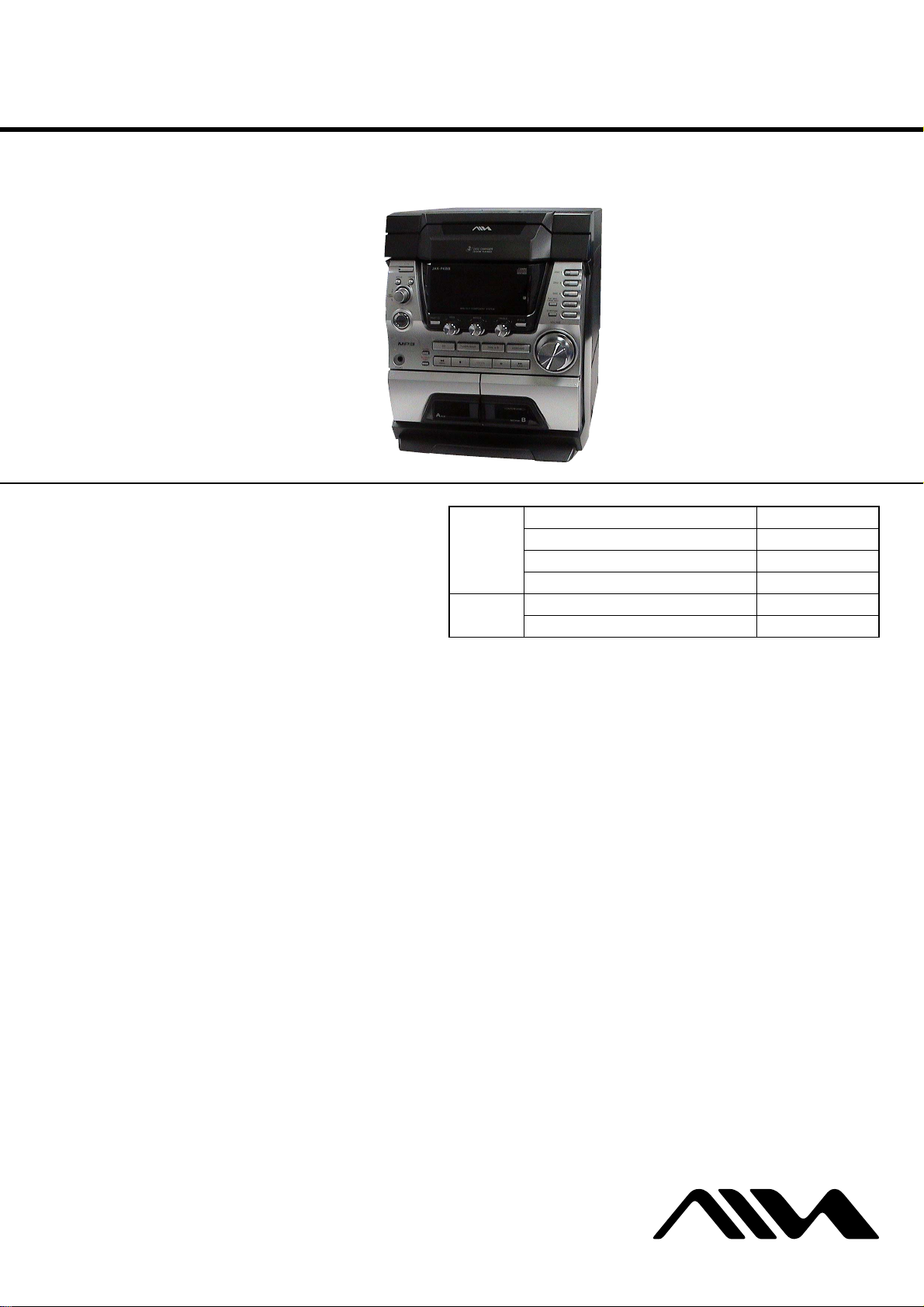
CX-JN88
Australian model:
Other models:
The following measured at AC 120, 220, 240 V
50/60 Hz
DIN power output (rated): 144 + 144 watts (6 ohms at
1kHz, DIN)
Continuous RMS power output (reference):
180 + 180 watts (6 ohms at
1kHz, 10% THD)
The following measured at AC 120, 220, 240 V
50/60 Hz
DIN power output (rated): 144 + 144 watts (6 ohms at
1kHz, DIN)
Continuous RMS power output (reference):
180 + 180 watts (6 ohms at
1kHz, 10% THD)
Inputs
VIDEO/MD IN (phono jacks):
voltage 450/250 mV,
impedance 47 kilohms
Amplifier section
European and Russian models:
DIN power output (rated): 100 + 100 watts (6 ohms at
1kHz, DIN)
Continuous RMS power output (reference):
125 + 125 watts (6 ohms at
1kHz, 10% THD)
Music power output (reference):
250 + 250 watts (6 ohms at
1kHz, 10% THD)
Outputs
PHONES (stereo mini jack):
accepts headphones of
8 ohms or more
SPEAKER: accepts impedance of 6 to
16 ohms
SURROUND SPEAKER:
accepts impedance of 6 to
16 ohms
CD player section
System Compact disc and dig i tal
audio system
Laser Semiconductor laser
(λ=780 nm)
Emission duration:
continuous
Frequency response 2 Hz – 20 kHz (±0.5 dB)
Signal-to-noise ratio More than 90 dB
Dynamic range More than 90 dB
Tape deck section
Recording system 4-track 2-channel, stereo
Frequency response 50 – 13,000 Hz (±3 dB),
using Sony TYPE I
cassettes
Tuner section
FM stereo, FM/AM superheterodyne tuner
FM tuner section
Tuning range
Russian models 65.0 – 74.0 MHz
(There is no stereo effect.
10-kHz step)
87.5 – 108.0 MHz
(50-kHz step)
Other models 87.5 – 108.0 MHz
(50-kHz step)
Antenna FM lead antenna
Antenna terminals 75 ohms unbalanced
Intermediate frequency 10.7 MHz
SERVICE MANUAL
Ver 1.0 2004.05
• CX-JN88 is the amplifier, CD play er , tape deck
and tuner section in JAX-N88/PK88.
CD CD Mechanism Type CDM74-F1BD81
Section Base Unit Name BU-F1BD81A
Tape deck Model Name Using Similar Mechanism CX-JN77
Section T ape Transport Mechanism Type CWM43FR34
AEP Model
E Model
Australian Model
Model Name Using Similar Mechanism CX-JN77
Optical Pick-up Block Name KSM-215DCP
9-877-788-01
2004E05-1
© 2004.05
Sony Corporation
Home Audio Company
Published by Sony Engineering Corporation
SPECIFICATIONS
COMPACT DISC DECK RECEIVER
– Continued on next page –
CX-JN88
AM tuner section
Tuning range
Pan-American models: 530 – 1,710 kHz
(with the tuning interval
set at 10 kHz)
531 – 1,710 kHz
(with the tuning interval
set at 9 kHz)
European and Russian models:
531 – 1,602 kHz (with the
tuning interval set at
9kHz)
Other models: 530 – 1,710 kHz
(with the tuning interval
set at 10 kHz)
531 – 1,602 kHz
(with the tuning interval
set at 9 kHz)
Antenna AM loop antenna
Antenna terminals External antenna te r minal
Intermediate frequency 450 kHz
General
Power requirements
European and Russian models:
230 V AC, 50/60 Hz
Australian models: 230 – 240 V AC, 50/60 Hz
Other models: 120 V, 220 V or
230 – 240 V AC, 50/60 Hz
Adjustable with voltage
selector
Notes on chip component replacement
• Never reuse a disconnected chip component.
• Notice that the minus side of a tantalum capacitor may be
damaged by heat.
Flexible Circuit Board Repairing
• Keep the temperature of the soldering iron around 270 ˚C
during repairing.
• Do not touch the soldering iron on the same conductor of the
circuit board (within 3 times).
• Be careful not to apply force on the conductor when soldering
or unsoldering.
CAUTION
Use of controls or adjustments or performance of procedures
other than those specified herein may result in hazardous radiation
exposure.
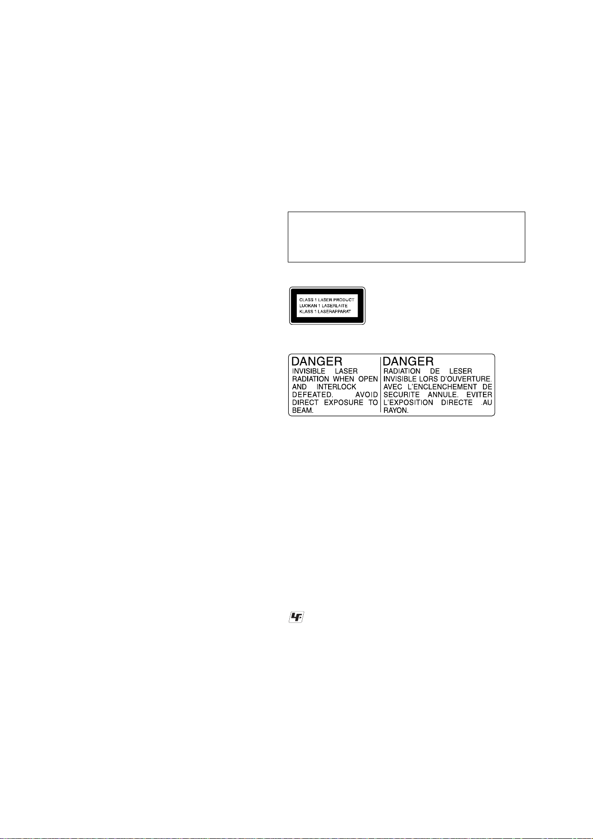
This appliance is classified as
a CLASS 1 LASER product.
The CLASS 1 LASER
PRODUCT MARKING is
located on the rear exterior.
Power consumption
European and Russian models:
205 watts
0.25 watts (at the Power
Saving Mode)
Other models: 180 watts
Dimensions (w/h/d) incl. projecting parts and controls
Amplifier/Tuner/Tape/CD section:
Approx. 280 × 325 ×
425 mm
Mass Approx. 9.9 kg
Design and specifications are subject to change
without notice.
SAFETY-RELATED COMPONENT WARNING!!
COMPONENTS IDENTIFIED BY MARK 0 OR DOTTED LINE
WITH MARK 0 ON THE SCHEMATIC DIAGRAMS AND IN
THE PARTS LIST ARE CRITICAL TO SAFE OPERATION.
REPLACE THESE COMPONENTS WITH SONY PARTS WHOSE
PART NUMBERS APPEAR AS SHOWN IN THIS MANUAL OR
IN SUPPLEMENTS PUBLISHED BY SONY.
UNLEADED SOLDER
Boards requiring use of unleaded solder are printed with the leadfree mark (LF) indicating the solder contains no lead.
(Caution: Some printed circuit boards may not come printed with
the lead free mark due to their particular size)
: LEAD FREE MARK
Unleaded solder has the following characteristics.
• Unleaded solder melts at a temperature about 40 °C higher
than ordinary solder.
Ordinary soldering irons can be used but the iron tip has to be
applied to the solder joint for a slightly longer time.
Soldering irons using a temperature regulator should be set to
about 350 °C.
Caution: The printed pattern (copper foil) may peel away if
the heated tip is applied for too long, so be careful!
• Strong viscosity
Unleaded solder is more viscou-s (sticky, less prone to flow)
than ordinary solder so use caution not to let solder bridges
occur such as on IC pins, etc.
• Usable with ordinary solder
It is best to use only unleaded solder but unleaded solder may
also be added to ordinary solder.
2

TABLE OF CONTENTS
CX-JN88
1. SERVICING NOTES ................................................ 4
2. GENERAL
Location of Controls........................................................ 7
3. DISASSEMBLY
3-1. Disassembly Flow ........................................................... 9
3-2. Case (Side-L/R) ............................................................... 10
3-3. Case (Top) ....................................................................... 10
3-4. Tray Panel........................................................................ 11
3-5. CD Mechanism Deck (CDM74-F1BD81) ...................... 11
3-6. Front Panel Block ............................................................ 12
3-7. Back Panel Section .......................................................... 12
3-8. MAIN Board.................................................................... 13
3-9. Tape Mechanism Deck (CWM43FR34).......................... 13
3-10. Table Assy ....................................................................... 14
3-11. MOTOR (TB) Board ....................................................... 14
3-12. MOTOR (LD) Board ....................................................... 15
3-13. Base Unit (BU-F1BD81A) .............................................. 15
3-14. CD Board ......................................................................... 16
4. TEST MODE.............................................................. 17
5. ELECTRICAL ADJUSTMENTS
CD Section ...................................................................... 21
6. DIAGRAMS
6-1. Block Diagram – SERVO Section – ............................... 22
6-2. Block Diagram – MAIN Section – ................................. 23
6-3. Block Diagram
– PANEL/POWER SUPPLY Section – ........................... 24
6-4. Printed Wiring Board – CD Board – .............................. 26
6-5. Schematic Diagram – CD Board – ................................. 27
6-6. Printed Wiring Boards – CHANGER Section –............. 28
6-7. Schematic Diagram – CHANGER Section – ................. 29
6-8. Printed Wiring Boards
– CDMP3 CONNECT/TRANSLATION Boards – ......... 30
6-9. Schematic Diagram
– CDMP3 CONNECT/TRANSLATION Boards – ......... 31
6-10. Schematic Diagram – MAIN Section (1/4) – ................. 32
6-11. Schematic Diagram – MAIN Section (2/4) – ................. 33
6-12. Schematic Diagram – MAIN Section (3/4) – ................. 34
6-13. Schematic Diagram – MAIN Section (4/4) – ................. 35
6-14. Printed Wiring Boards – MAIN Section – ..................... 36
6-15. Printed Wiring Board – PANEL Section – ..................... 37
6-16. Schematic Diagram – PANEL Section (1/2) – ............... 38
6-17. Schematic Diagram – PANEL Section (2/2) – ............... 39
6-18. Printed Wiring Board – POWER AMP Section –
(AEP, CIS only) ............................................................... 40
6-19. Schematic Diagram – POWER AMP Section –
(AEP, CIS only) ............................................................... 41
6-20. Printed Wiring Board – POWER AMP Section –
(E51, AUS only) .............................................................. 42
6-21. Schematic Diagram – POWER AMP Section –
(E51, AUS only) .............................................................. 43
6-22. Printed Wiring Boards – TRANS Section –
(AEP, CIS only) ............................................................... 44
6-23. Schematic Diagram – TRANS Section –
(AEP, CIS only) ............................................................... 45
6-24. Printed Wiring Boards – TRANS Section –
(E51, AUS only) .............................................................. 46
6-25. Schematic Diagram – TRANS Section –
(E51, AUS only) .............................................................. 47
7. EXPLODED VIEWS
7-1. Case Section .................................................................... 58
7-2. Tape Mechanism Deck Section (CWM43FR34)............. 59
7-3. Cassette Box Section ....................................................... 60
7-4. Front Panel Section ......................................................... 61
7-5. Back Panel Section .......................................................... 62
7-6. Chassis Section ................................................................ 63
7-7. CD Mechanism Deck Section-1 (CDM74-F1BD81) ...... 64
7-8. CD Mechanism Deck Section-2 (CDM74-F1BD81) ...... 65
7-9. CD Mechanism Deck Section-3 (CDM74-F1BD81) ...... 66
7-10. Base Unit Section (BU-F1BD81A) ................................. 67
8. ELECTRICAL PARTS LIST................................ 68
• Abbreviation
AUS: Australian model
E51 : Chilean and Peruvian models
3
CX-JN88
SECTION 1
SERVICING NOTES
NOTES ON HANDLING THE OPTICAL PICK-UP
BLOCK OR BASE UNIT
The laser diode in the optical pick-up block may suffer electrostatic
break-down because of the potential difference generated by the
charged electrostatic load, etc. on clothing and the human body.
During repair, pay attention to electrostatic break-down and also
use the procedure in the printed matter which is included in the
repair parts.
The flexible board is easily damaged and should be handled with
care.
NOTES ON LASER DIODE EMISSION CHECK
The laser beam on this model is concentrated so as to be focused on
the disc reflective surface by the objective lens in the optical pickup block. Therefore, when checking the laser diode emission,
observe from more than 30 cm away from the objective lens.
LASER DIODE AND FOCUS SEARCH OPERATION
CHECK
Carry out the “S curve check” in “CD section adjustment” and check
that the S curve waveforms is output three times.
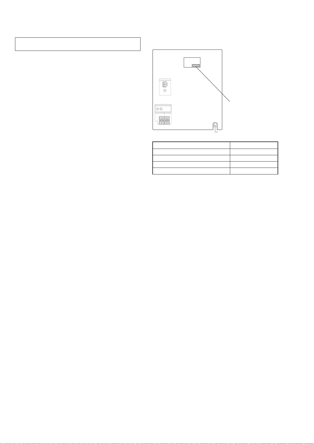
• MODEL IDENTIFICATION
– Rear View –
PART No.
RLRL
+
+
–
–
MODEL PART No.
Chilean and Peruvian models 4-253-929-0[]
AEP model 4-253-948-0[]
CIS model 4-253-953-0[]
Australian model 4-255-532-0[]
4
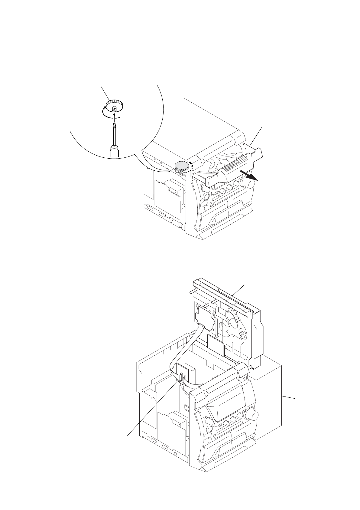
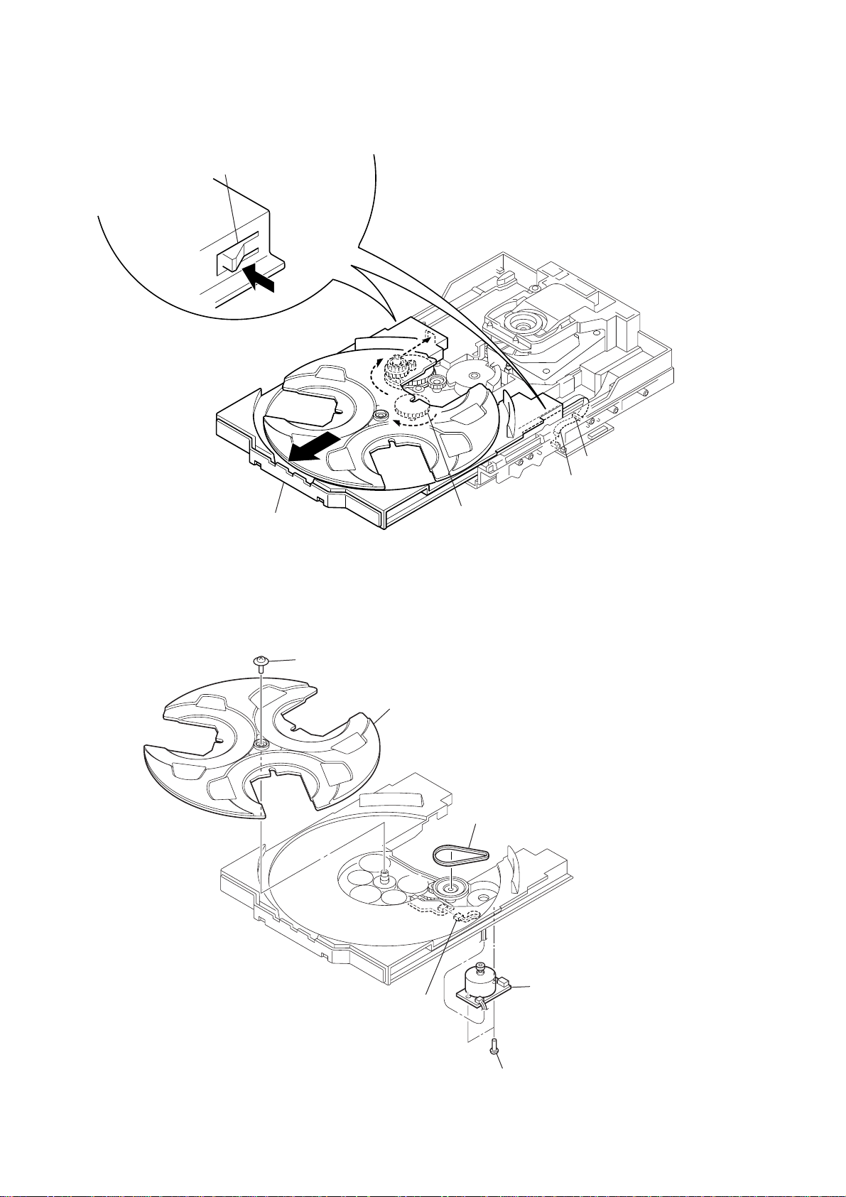
HOW TO OPEN THE DISC TRAY WHEN POWER SWITCH TURNS OFF.
1
Remove the case (side-L).
2
Turn the loading gear in the direction
of arrow A.
A
Pull-out the disc tray.
3
CX-JN88
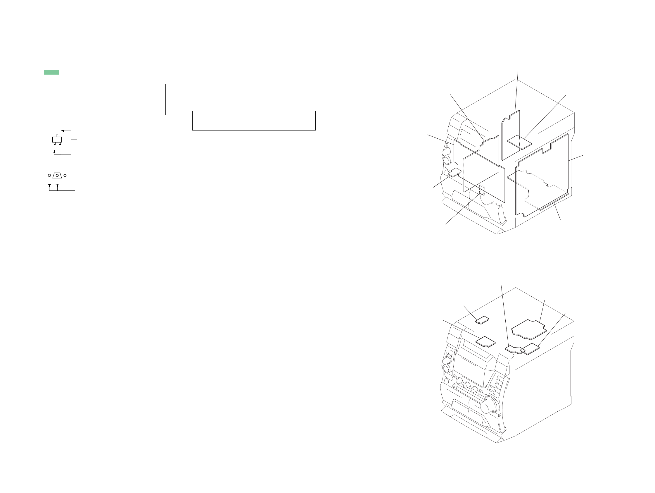
SERVICE POSITION
– CD MECHANISM DECK –
CD mechanism deck
stand
CDMP3 CONNECT board
5
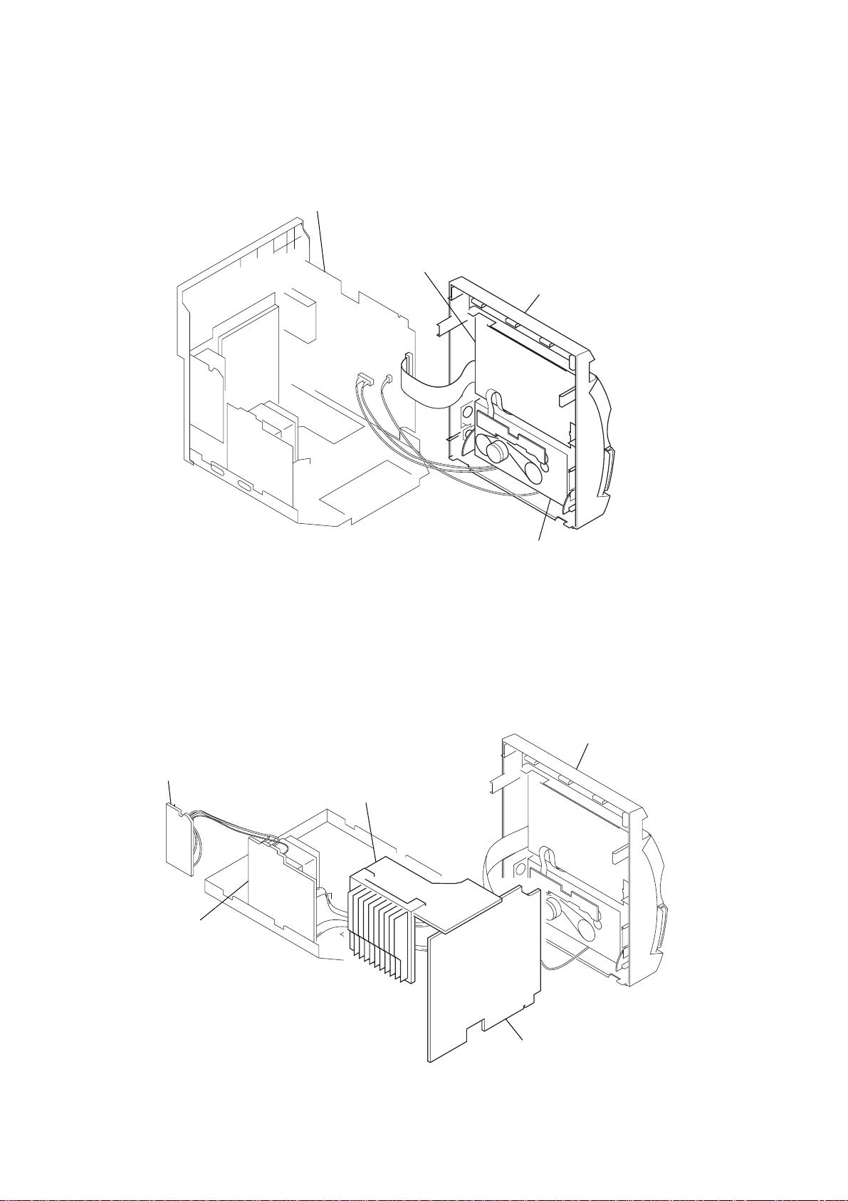
CX-JN88
– FRONT PANEL SECTION –
MAIN board
PANEL board
front panel section
– AMP BOARD –
TRANS board
tape mechanism deck
front panel section
SUB TRANS board
POWER board
MAIN board
6
4q
q
qkqlw;waw
1
2
3 5 6 7
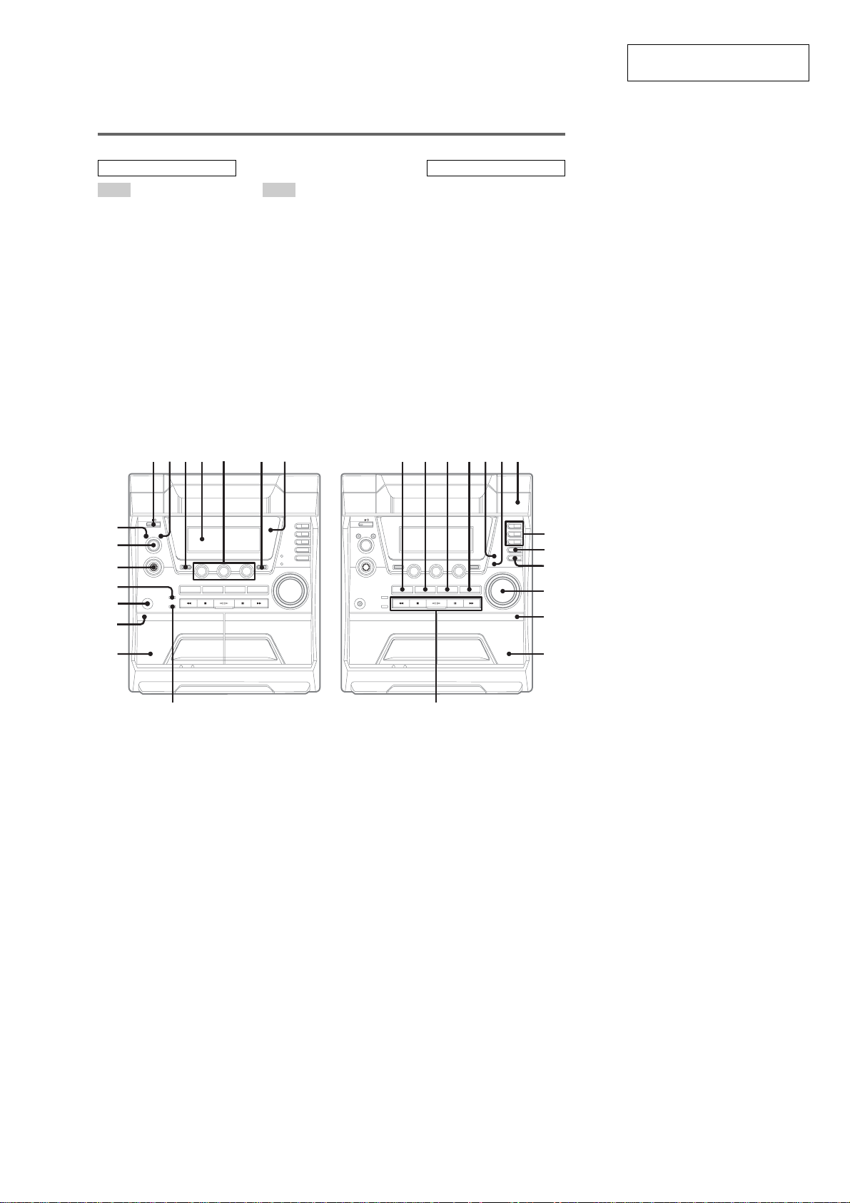
• LOCATION OF CONTROLS
Main unit
ALPHABETICAL ORDER
A – N O – Z
ALBUM + wl
ALBUM – wl
BASS control 5
CD qh
CD SYNC qs
Deck A 9
Deck B wk
DISC 1 – 3 wd
DISC SKIP/EX-CHANGE wf
Disc tray ws
DISPLAY qg
Display window 4
ENTER 2
i-Bass qd
MIDDLE control 5
Operation Dial
P FILE 6
PHONES jack qa
PLAY MODE w;
PRESET EQ 3
REC PAUSE/START 8
Remote sensor 7
SURROUND wa
TAPE A/B qk
TREBLE control 5
TUNER/BAND qj
TUNING MODE w;
VIDEO/MD ql
VOLUME control wh
(AMS/TUNING) qf
SECTION 2
GENERAL
BUTTON DESCRIPTIONS
?/1 (power) 1
Z PUSH (deck A) (eject) 0
Z (eject) wg
PUSH Z (deck B) (eject) wj
m (rewind) wl
x (stop) wl
hH
(play) wl
X (pause) wl
M (fast forward) wl
CX-JN88
This section is extracted from
instruction manual.
qg
qf
qd
qs
qa
0
9
j
h
s
wd
+–
++–
+–+–
–
Z Z
+–
++–
+–+–
–
wf
wg
wh
wj
wk
wl8
7
CX-JN88
Remote control
ALPHABETICAL ORDER
A – E
ALBUM + qa
ALBUM – qd
CD qk
CLEAR qg
CLOCK/TIMER SELECT 2
CLOCK/TIMER SET 3
DISC SKIP 0
DISPLAY wa
ENTER 9
EQ qf
F–Z
FM MODE 4
FUNCTION 6
PLAY MODE w;
REPEAT 4
SLEEP ws
TAPE qj
TUNER BAND 5
TUNER MEMORY ql
TUNING MODE w;
VOLUME +/– qs
ws
wa
w;
ql
qk
qj
qh
BUTTON DESCRIPTIONS
?/1 (power) 1
m/M (rewind/fast forward)
7
N (play) 8
X (pause) 8
x (stop) 8
–/+ (tuning) qh
./> (goback/go forward)
qh
1
2
3
4
5
6
7
8
Setting the clock
Use buttons on the remote for the operation.
1
Press ?/1 to turn on the system.
2
Press CLOCK/TIMER SET.
3
Press . or > repeatedly to set the
hour.
4
Press ENTER.
5
Press . or > repeatedly to set the
minute.
6
Press ENTER.
The clock starts working.
To adjust the clock
1
Press CLOCK/TIM ER SET.
2
Press . or > repeatedly to select
“CLOCK SET”, then press ENTER.
3
Do the same procedures as step 3 to 6
above.
Notes
•The clock settings are canceled when you disconnect
the power cord or if a power failure occurs.
•You cannot set the clock in Power Saving Mode.
qg
qf
qd
9
q;
qa
qs
8
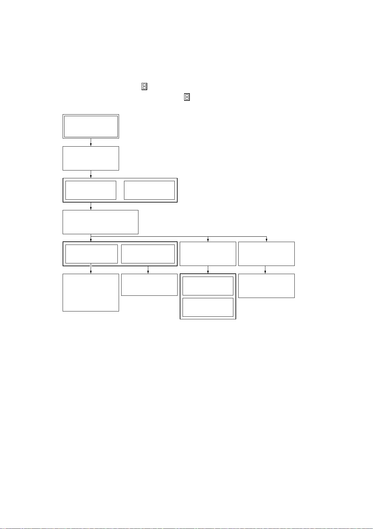
• This set can be disassembled in the order shown below.
3-1. DISASSEMBLY FLOW
Note 1: The process described in can be performed in any order.
Note 2: Without completing the process described in , the next process can not be performed.
SET
3-2. CASE
(SIDE-L/R)
(Page 10)
CX-JN88
SECTION 3
DISASSEMBLY
3-3. CASE (TOP)
(Page 10)
3-5. CD MECHANISM DECK
(CDM74-F1BD81)
(Page 11)
3-6. FRONT PANEL
BLOCK
(Page 12)
3-9. TAPE
MECHANISM
DECK
(CWM43FR34)
(Page 13)
3-4. TRAY PANEL
3-7. BACK PANEL
3-8. MAIN BOARD
(Page 11)
SECTION
(Page 12)
(Page 13)
3-10. TABLE ASSY
(Page 14)
3-11. MOTOR (TB)
BOARD
(Page 14)
3-12. MOTOR (LD)
BOARD
(Page 15)
3-13. BASE UNIT
(BU-F1BD81A)
(Page 15)
3-14. CD BOARD
(Page 16)
9
CX-JN88
Note: Follow the disassembly procedure in the numerical order given.
3-2. CASE (SIDE-L/R)
1
two screws
(case 3 TP2)
2
screw
(case 3 TP2)
3
two screws
(BVTP3 × 10)
7
case (side-R)
3-3. CASE (TOP)
4
case (side-L)
2
case (top)
5
three screws
(case 3 TP2)
1
two screws
(BVTP3
×
10)
6
two screws
(BVTP3 × 10)
10
3-4. TRAY PANEL
1
Turn the loading gear
in the direction of arrow A.
A
four claws
B
C
3
Remove the tray panel
in the direction of arrow C.
2
Pull-out the tray in the direction
of arrow B.
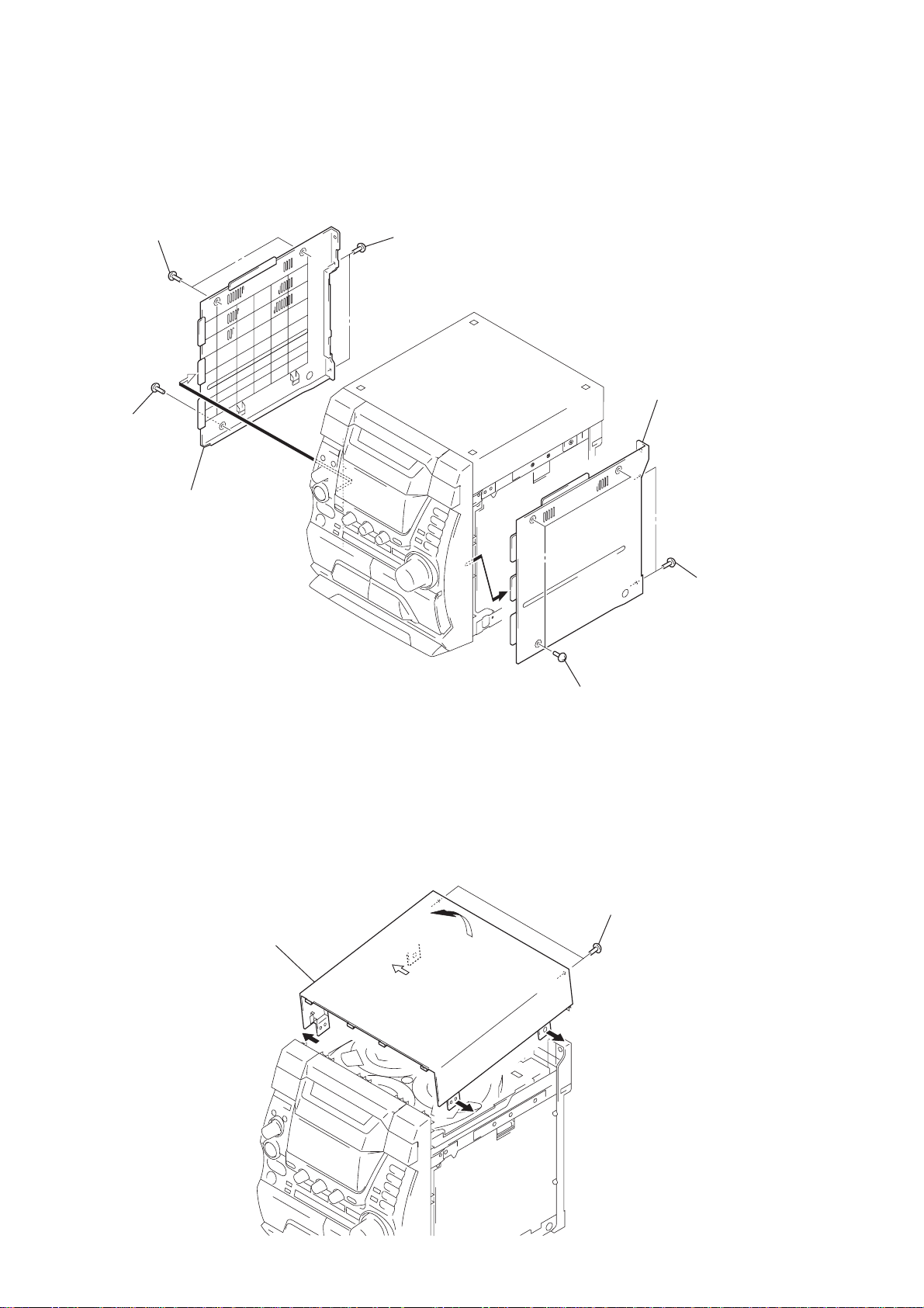
CX-JN88
3-5. CD MECHANISM DECK
(CDM74-F1BD81)
5
wire (flat type) (17 core)
(CN873)
2
screw
(BVTP3
×
10)
4
7
CD mechanism deck (CDM74-F1BD81)
6
two connectors
(CN701, CN874)
3
three screws
(BVTP3
×
10)
1
screw
(BVTP3
×
10)
11
CX-JN88
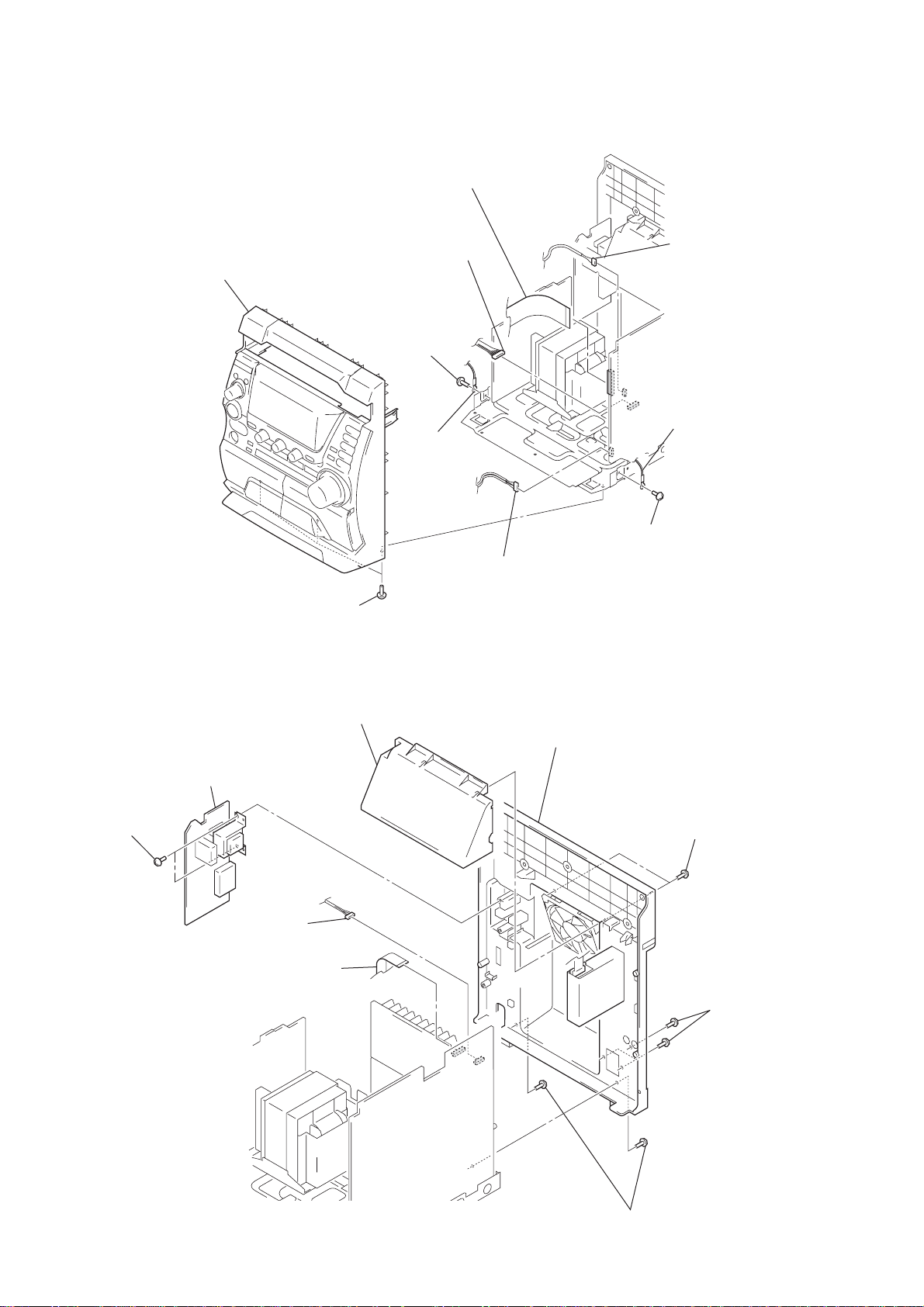
3-6. FRONT PANEL BLOCK
•
Abbreviation
AUS: Australian model
E51 : Chilean and Peruvian models
8
front panel block
1
wire (flat type) (31 core) (AEP)/
wire (flat type) (29 core) (CIS, E51, AUS)
(CN302)
2
connector
(CN103)
3
screw
(BVTP3
4
×
8)
harness
2
connector
(CN112)
6
harness
3-7. BACK PANEL SECTION
•
Abbreviation
AUS: Australian model
E51 : Chilean and Peruvian models
8
SUB TRANS board
7
two screws
(BVTP3
×
10)
2
connector
(CN308)
1
wire (flat type) (11 core) (CIS, E51, AUS)/
wire (flat type) (15 core) (AEP)
(CN101)
7
three screws
(BVTP3
×
8)
4
duct cover
2
connector
(CN309)
9
back panel section
5
screw
(BVTP3
3
×
8)
two screws
(BVTP3
×
5
10)
three screws
(BVTP3
×
10)
12
6
two screws
(BVTP3
×
10)
3-8. MAIN BOARD
1
connector
(CN907)
4
3
connector
(CN307)
CX-JN88
MAIN board
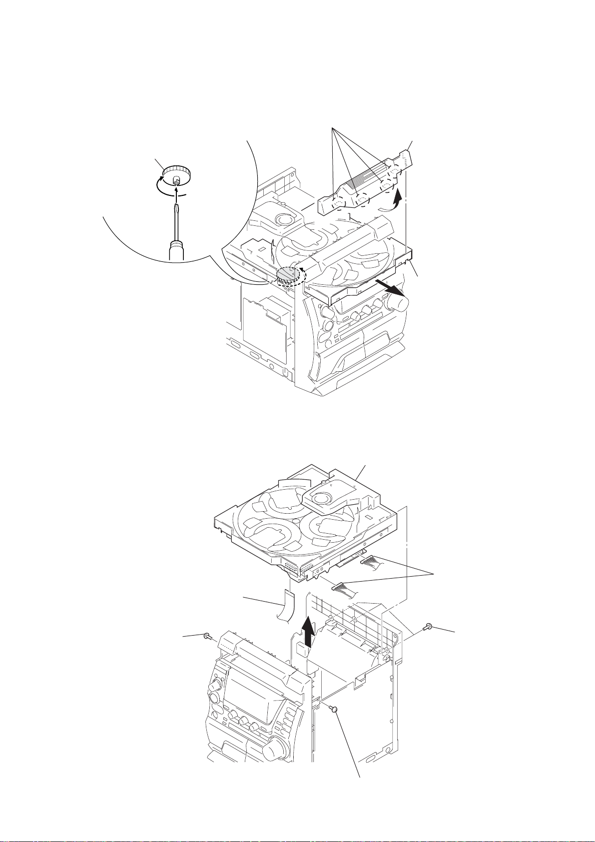
3-9. TAPE MECHANISM DECK
(CWM43FR34)
2
two screws
(BVTP3
2
TRANSLATION board
(AEP, CIS)
×
8)
1
six screws
(BVTP2.6 × 8)
3
tape mechanism deck (CWM43FR34)
13
CX-JN88
)
3-10. TABLE ASSY
two claws
5
A
2
Pull-out the table assy.
6
table assy
3-11. MOTOR (TB) BOARD
1
screw
(PTPWH M2.6)
2
table (loading)
1
Turn the loading gear
in the direction of arrow
3
belt (table)
4
hook
3
wire (flat type) (5 core
(CN702)
A
.
14
4
connector
(CN731)
6
5
two screws
(BTTP M2.6)
MOTOR (TB) board
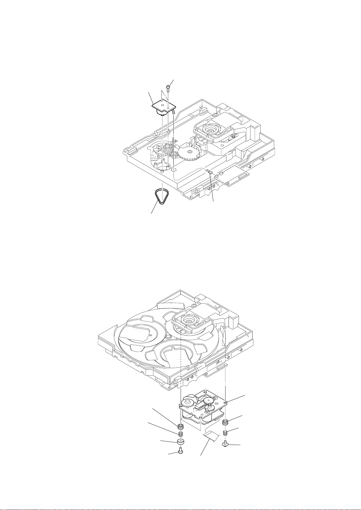
3-12. MOTOR (LD) BOARD
4
MOTOR (LD) board
3
two screws
(BTTP M2.6)
CX-JN88
1
3-13. BASE UNIT (BU-F1BD81A)
belt (loading)
2
connector
(CN704)
5
4
three coil springs
(insulator)
3
three stoppers (BU)
three insulators
2
three screws
(BTTP M2.6)
1
wire (flat type) (27 core)
(CN201)
9
base unit (BU-F1BD81A)
8
insulator
7
coil spring
(insulator)
6
floating screw
(PTPWHM2.6)
15
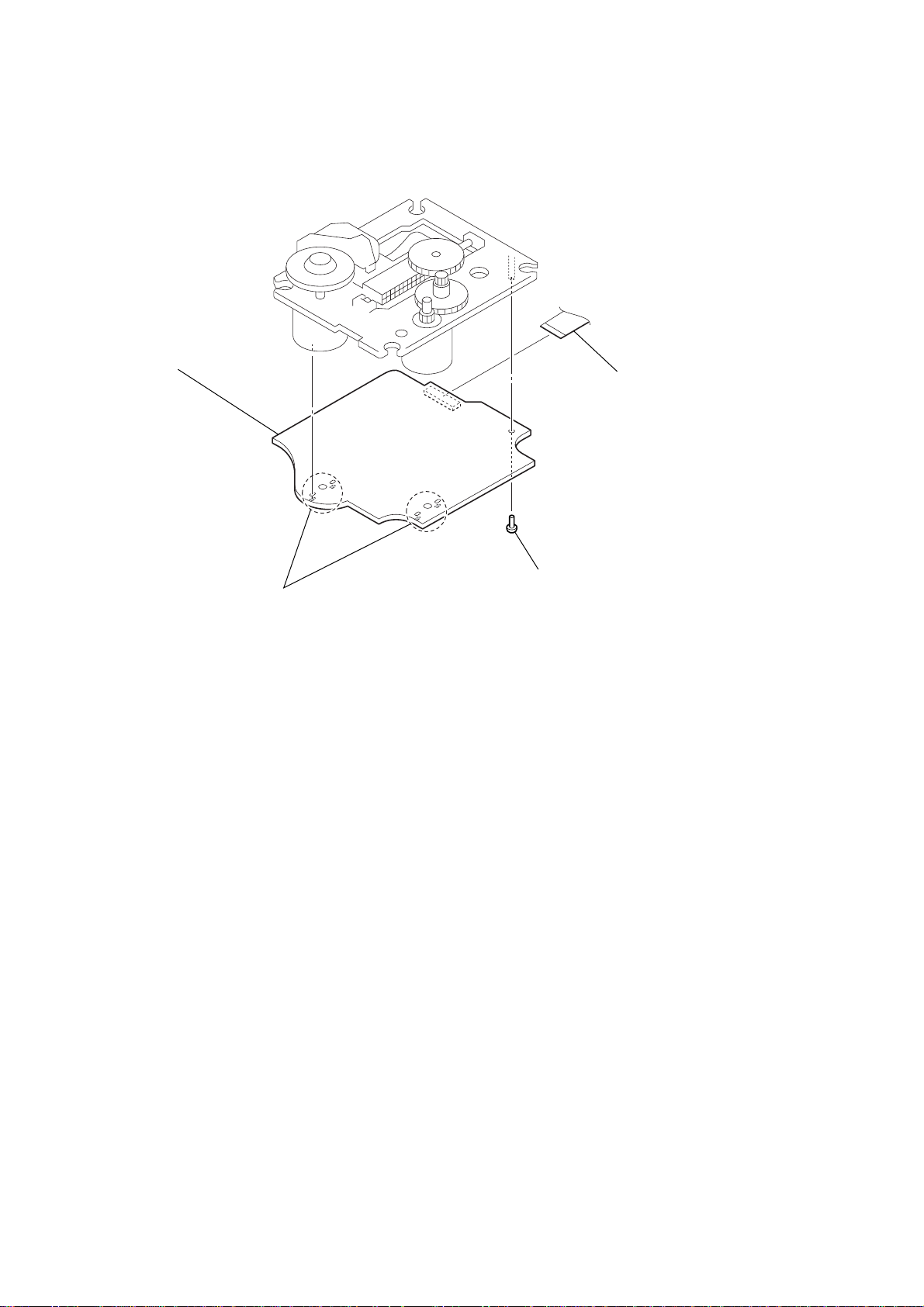
CX-JN88
)
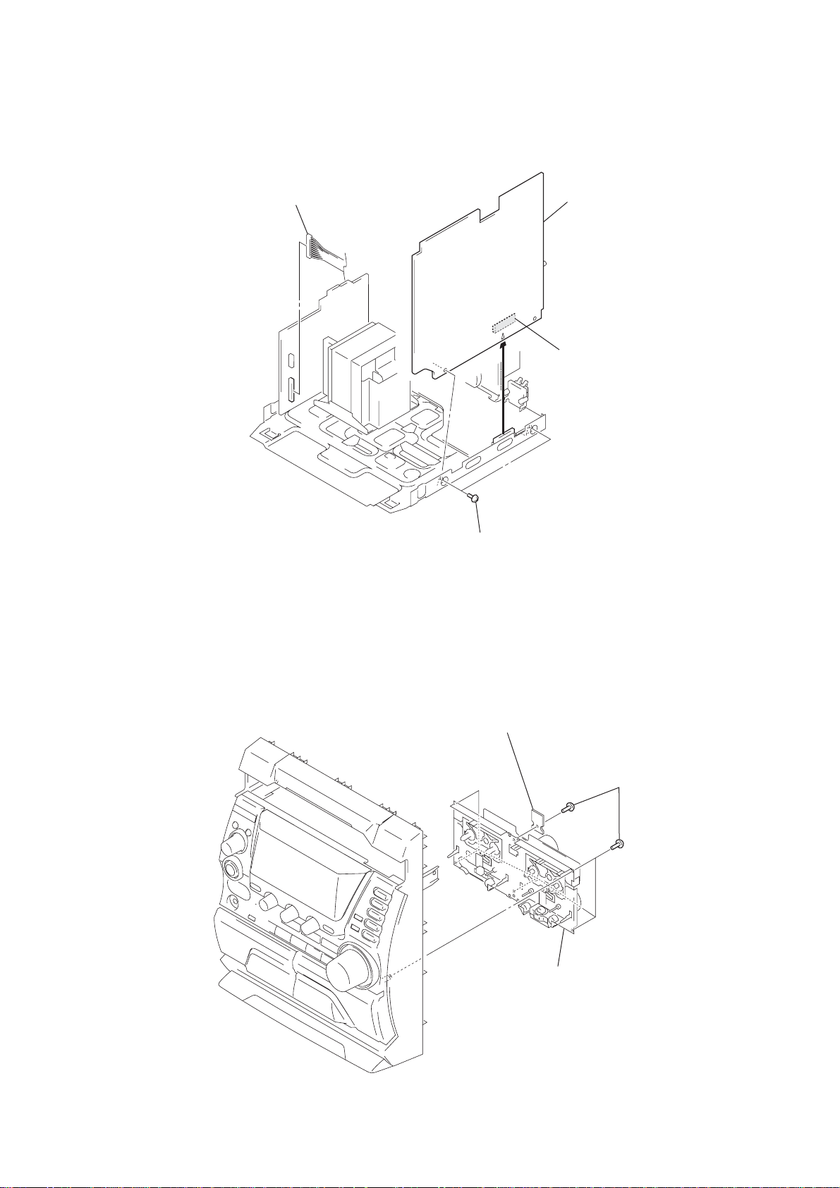
3-14. CD BOARD
4
CD board
2
wire (flat type) (16 core
(CN101)
1
Remove four solders.
3
screw (2.6 × 8)
16

SECTION 4
TEST MODE
CX-JN88
MC COLD RESET
The cold reset clears all data including preset data stored in the
RAM to initial conditions. Execute this mode when returning the
set to the customer.
Procedure:
1. Press the I/1 button to turn the power ON.
2. Press three buttons of x , [P FILE] and [DISC 1] simultane-
ously.
3. The message “COLD RESET” is displayed on the fluorescent
indicator tube momentarily, then becomes standby states.
AM TUNING INTERVAL CHANGE-OVER
(Except AEP, CIS models)
A step of AM tuning interval can be changed over between 9 kHz
and 10 kHz.
Procedure:
1. Press the I/1 button to turn the power on.
2. Press the [TUNER/BAND] button to select “AM”.
3. Press the I/1 button to turn the power off.
4. Press two buttons of [PLAY MODE/TUNING MODE] and I/1
simultaneously.
5. The message “AM 9K STEP” or “ AM 10K STEP” is displayed
on the fluorescent indicator tube, and thus the channel step is
changed over.
CD SHIP (LOCK) MODE
This mode moves the optical pick-up to the position durable to
vibration. Use this mode when returning the set to the customer
after repair.
Procedure:
1. Press the I/1 button to turn the power on.
2. Press the [CD] button to select “CD”.
3. Press two buttons of [CD] and [POWER] simultaneously.
4. The message “LOCK” is displayed on the fluorescent indicator
tube, and the CD ship mode is set.
CD SHIP (LOCK) MODE & COLD RESET
This mode is used to perform CD chip (lock) mode and cold reset
simultaneously.
Procedure:
1. Press the I/1 button to turn the power on.
2. Press the [CD] button to select “CD”.
3. Press three buttons of x , [CD] and [POWER] simultaneously.
4. The message “COLD RESET” is displayed on the fluorescent
indicator tube momentarily, then becomes standby states.
CD TRAY LOCK MODE
This mode is used to unable to take sample disc out of tray in the
shop.
Procedure:
1. Press the I/1 button to turn the power on.
2. Press the [CD] button to select “CD”.
3. Set disc on the CD tray, press two b uttons of x and Z for 5
seconds.
4. The message “LOCKED” is displayed on the fluorescent
indicator tube and the CD tray is locked. (Even if pressing
the Z button, the message “LOCKED” is displayed on the
fluorescent indicator tube and the CD tray is locked)
5. To release from this mode, press two b uttons of x and Z for
5 seconds.
6. The message “UNLOCKED” is displayed on the fluorescent
indicator tube and the CD tray is unlocked.
AMP TEST MODE
This mode is used to display the parameter of amplifier IC and
display the VACS status.
Procedure:
1. Press the I/1 button to turn the power on.
2. Press three buttons of x , [P FILE] and [PLAY MODE/TUNING
MODE] simultaneously.
3. When the AMP test mode is activated, the message “AMP
TEST IN” is displayed on the fluorescent indicator tube
momentarily, then amplif ier adjustment mode is displayed on
the fluorescent indicator tube.
4. Press the [DISPLAY] button to changed over between VACS
status display mode and the amplifier IC parameter display
mode.
5. In the amplifier IC parameter display mode, press the [i-BASS]
button to changed over DBFB on/off, and when it is on, the
character “D” is displayed on the fluorescent indicator tube.
6. In the amplifier IC parameter display mode, press the
[SURROUND] button to changed over surround on/off, and
when it is on, the character “S” is displayed on the fluorescent
indicator tube.
7. In the amplifier IC parameter display mode, turn each knob of
[BASS], [MIDDLE] and [TREBLE] causes respective parameters
to be changed, as well as change-over of the display on the
fluorescent indicator tube.
CHANGE-OVER FUNCTION OF MD/VIDEO
This mode is used to enable function of external input to change
over between MD and VIDEO.
Procedure:
1. Press the I/1 button to turn the power on.
2. Press two buttons of VIDEO (MD) and I/1 simultaneously.
3. The message “MD” or “VIDEO”is displayed on the fluorescent
indicator tube, and the function of external input is changed
over.
17
CX-JN88
AGING MODE
This mode can be used for operation check of CD section and tape
deck section.
CD section and tape deck section work in parallel.
If an error occurred:
The aging operation stops only an error occurred sections and display
then status.
If no error occurs:
The aging operation continues repeatedly.
Procedure:
1. Press the I/1 button to turn the power on.
2. Press the [CD] button to select “CD”.
3. Set disc on the CD tray and set tape into the deck.
4. Press three b uttons of x , [P FILE] and [DISC SKIP/EX-CHANGE]
simultaneously.
5. Aging operations of CD and tape are started at the same time.
6. To release from this mode, press the I/1 button to turn the
power off and press the function buttons.
1. Display at the Aging Mode
Display operating state of CD section and tape deck section
alternately.
If an error occurred, stop display which that section.
2. CD Section
The sequence during the aging mode is following as below.
Display at the aging mode is the same as the normal operation.
Aging mode sequence (CD section) :
3. Tape Deck Section
The sequence during the aging mode is following as below.
If an error occurred, stop display that step.
Aging mode sequence (tape deck section) :
Rewind the tape A and B
“TAPE AAG-1 or TAPE BAG-2”
Shut off
FWD play the tape A
“TAPE AAG-3”
2 minutes
Rewind the tape A
“TAPE AAG-6”
Shut off
FWD play the tape B
“TAPE BAG-3”
2 minutes
Rewind the tape B
“TAPE BAG-6”
Shut off
Start (from disc 1)
Disc chucking
TOC read
Play first track for 2 seconds
Play last track for 2 seconds
EX-change open/close
Open the disc tray
Disc skip
Close the tray
Change the next disc.
Note: “TAPE *AG-*” is display of each step.
PANEL TEST MODE
This mode is used to check the fluorescent indicator tube, LEDs
and buttons.
Procedure:
1. Press the I/1 button to turn the power on.
2. Press three buttons of x , [P FILE] and [ENTER] simultaneously.
3. Fluorescent indicator tube and LEDs are all turned on.
4. Press two buttons of X and [ENTER] simultaneously, mode
is changed over.
5. In the key check mode, press each key , the defined ke y number
of every each key list is displayed on the fluorescent indica tor
tube.
6. In the key count check mode, “KEYCNT 0” is displayed on
the fluorescent indicator tube. Each time a key is pressed, “K”
value increases. Howe ver , once a key is pressed, it is no longer
taken into account.
7. In the headphone input check mode, connect the headphone,
the message “H_P ON” is displayed on the fluorescent
indicator tube, and disconnect the headphone, the message
“H_P OFF” is displayed on the fluorescent indicator tube.
8. In the volume check mode, “VOLUME FLAT” is displayed
on the fluorescent indicator tube. Turn the [VOLUME] knob
clockwise, the message “VOLUME UP” is displayed on the
fluorescent indicator tube momentarily and turn the [VOLUME]
knob counterclockwise, the message “VOLUME DOWN” is
displayed on the fluorescent indicator tube momentarily.
18
CX-JN88
MC TEST MODE
This mode is used to check operations of microprocessor.
Procedure:
1. Press the I/1 button to turn the power on.
2. Press three buttons of x , [P FILE] and [DISC 3] simultaneously.
3. When the MC test mode is activated, VACS le v el is displayed
on the fluorescent indicator tube momentarily.
4. Turn the [AMS/TUNING] knob clockwise, the message “ALL
EQ MAX” is displayed on the fluorescent indicator tube
momentarily and turn the [AMS/TUNING] knob counterclockwise, the message “ALL EQ MIN” is displayed on the
fluorescent indicator tube momentarily.
5. Press the [PRESET EQ] button, the message “ ALL EQ FLAT”
is displayed on the fluorescent indicator tube momentarily.
6. Turn the [VOLUME] knob clockwise, the message “V OLUME
MAX” is displayed on the fluorescent indicator tube
momentarily and turn the [VOLUME] knob counterclockwise,
the message “VOLUME MIN” is displayed on the fluorescent
indicator tube momentarily.
7. Press the [i-BASS] button to changed over VACS on/off.
8. When the [REC PAUSE/START] button is pressed twice with a
tape set in the deck-B, the function is switched “MD” or
“VIDEO” and recording starts. When the m or M button
is pressed during recording, the tape is rewound back to the
beginning of recording, the function is switched to “TAPE
B”, then playback starts.
9. When the [CD SYNC] key is pressed with the test tape (AMS-
100, AMS-110A) in the deck, number of space between tunes
is counted, then if AMS-110A is set, “OK” is displayed on the
fluorescent indicator tube and if AMS-100 is set, “NG” is
displayed on the fluorescent indicator tube.
10. Press the I/1 button to release from this mode, then cold reset
is performed.
VERSION DISPLAY MODE
This mode is used to check the model, destination and software
version.
Procedure:
1. Press the I/1 button to turn the power on.
2. Press three buttons of x , [P FILE] and [DISC 2] simultaneously.
3. When this mode is activated, model and destination is displayed
on the fluorescent indicator tube.
4. Press the [DISPLAY] button to changed ov er between software
version and year, month, day of the software creation display
mode and model and destination display mode.
5. To release from this mode, press three b uttons of x , [P FILE]
and [DISC 2] simultaneously.
CD ERROR CODE DISPLAY MODE
This mode can be used for error code display of CD section.
Procedure:
1. Press the I/1 button to turn the power on.
2. Press the [CD] key to select “CD”.
3. Press three buttons of x , [CD] and [DISC 1] simultaneously.
4. When this mode is activated, mechanism deck error code is
displayed on the fluorescent indicator tube.
5. Press the [i-BASS] button to c hanged over between optical pickup error code display mode and mechanism deck error code
mode.
6. Turn the [AMS/TUNING] knob to change ov er display of error
history.
1. Mechanism Deck Error Code Mode
When this mode is entered, mechanism deck error code is displayed
with the 10-character format on the fluorescent indicator tube.
The first digit from the left indicates:
The first digit from the left indicates which mode the error history
is. In the mechanism deck error code mode, “M” is displayed on
the fluorescent indicator tube.
The second digit from the left indicates:
(Error history No. display)
The second digit from the left indicates which order the error history
is. “1” indicates the latest error history, and each time the number
increases by one, the error history goes back to one-previous error .
The third and 4th digit from the left indicates:
(Error status display)
The third and 4th digit from the left indicates which error status is
indicated.
Display Status
00 No error
08 Table operation time-out (Table does not mo ve to the target
position within the specified time)
16 In the chucking down oper ation, the operation was retried
by the maximum number of times but the operation could
not be completed
17 In the chucking up and down operation, the reverse
recovery processing was attempted but it could not be
recovered
18 In the chucking up operation, the operation was retried by
the maximum number of times but the operation could not
be completed
20 Loading operation time-out (Table does not move to the
target position within the specified time)
22 As the chuck was in the e x-open status at the initialization,
the closing was attempted but could not be completed
The 5th and 6th digit from the left indicates:
(Present status display)
The 5th and 6th digit from the left indicates which operating status
when an error occurred is indicated.
Display Status
01 Open completion status
02 From open status, the mov ement to chucking down position
is under way
03 From chucking down position, the open operation is under
way
04 Chucking down completion status
10 The chucking down operation is under way
11 The chucking up operation is under way
12 Close completion status
13 From close status, the ex-open operation is under way
14 From ex-open status, the close operation is under way
18 Ex-pen completion status
19

CX-JN88
The 7th and 8th digit from the left indicates:
(Motor status display)
The 7th and 8th digit from the left indicates which motor output
status when an error occurred is indicated.
Display Status
× 0 No table motor output
× 1Table motor forward output
× 2Table motor backward output
× 3Table motor break output
0 × No loading motor output
1 × Loading motor forward output
2 × Loading motor backward output
3 × Loading motor break output
The 9th and 10 th digit from the left indicates:
(Tray status display)
The 9th and 10th digit from the left indicates which target processing
when an error occurred is indicated.
Display Status
01 Open operation
12 Close operation
18 Ex-open operation
2. Optical Pick-up Error Code Mode
When this mode is entered, optical pick-up error code is displayed
with the 8-character format on the fluorescent indicator tube.
The first digit from the left indicates:
The first digit from the left indicates which mode the error history
is. In the optical pick-up error code mode, “D” is displayed on the
fluorescent indicator tube.
The second digit from the left indicates:
(Error history No. display)
The second digit from the left indicates which order the error history
is. “1” indicates the latest error history, and each time the number
increases by one, the error history goes back to one-previous error .
The 5th and 6th digit from the left indicates:
(Error step display)
The 5th and 6th digit from the left indicates which processing when
a trouble occurred
Display Contents
01 Power OFF in progress
02 Initialize in progress
03 Oscillation stopping
04 From oscillation stop, oscillation starting
05 Stopping
06 Stop operation is under way
07 Start operation in progress
08 TOC read in progress
09 Search operation is under way
0A Playback operation is under way
0B Pause operation is under way
0C Playback manual search operation is under way
0D Pause manual search operation is under way
0E —
The 7th and 8th digit from the left indicates:
The 7th and 8th digit from the left indicates which operation in
progress when a trouble occurred. (Step of each processing of the
5th and 6th digits is indicated)
5 REPEAT LIMIT CANCEL MODE
Number of repeat for CD playback is 5 times when the repeat mode
is “REPEAT”. This mode is used to enables CD to repeat playback
for limitless times.
Procedure:
1. Press the I/1 button to turn the power on.
2. Press the [CD] button to select “CD”.
3. Press three buttons of x , [CD] and [ENTER] simultaneously.
4. The message “LIMIT OFF” is displayed on the fluorescent
indicator tube momentarily, CD repeat 5 limit is cancelled.
The third and 4th digit from the left indicates:
(Error status display)
The third and 4th digit from the left indicates which error status is
indicated.
Display Status
01 Not focused (TOC read without a disc)
02 GFS NG (TOC read with a disc chucked)
03 Start operation time-over
04 Defocused continuously (Defocused during TOC reading)
05 Q code not entered for specified time
06 Tracking not turned ON
07 Blank disc (Blank disc TOC read)
20
e
symmetry
S-curve waveform
within 3
±
0.5 Vp-p
A
B
p
SECTION 5
ELECTRICAL ADJUSTMENTS
CX-JN88
CD SECTION
Note:
1. CD Block is basically designed to operate without adjustment.
Therefore, check each item in order given.
2. Use YEDS-18 (3-702-101-01) unless otherwise indicated.
3. Use an oscilloscope with more than 10MW impedance.
4. Clean the object lens by an applicator with neutral detergent when the
signal level is low than specified value with the following checks.
S-CURVE CHECK
oscilloscop
CD board
TP(FE)
TP(VC)
Procedure:
1. Connect an oscilloscope to TP (FE) and TP (VC) on the CD
board.
2. Press the I/1 button to turn the power on.
3. Load a disc (YEDS-18) and actuate the focus search. (In
consequence of open and close the disc tray, actuate the focus
search)
4. Confirm that the oscilloscope waveform (S-curve) is
symmetrical between A and B. And confirm peak to peak le vel
within 3 ± 0.5 Vp-p.
RF signal waveform
VOLT/DIV : 200mV
TIME/DIV : 500ns
– CD BOARD (Conductor Side) –
TP
(VC)
level : 1.3
±
0.3 Vp-
Note: • Try to measure several times to make sure than the ratio of A : B
or B : A is more than 10 : 7.
• Take sweep time as long as possible and light up the brightness
to obtain best waveform.
Connecting Location: CD board
RFAC LEVEL CHECK
oscilloscope
CD board
TP(RFACO)
TP(VC)
Procedure:
1. Connect an oscilloscope to TP (RFACO) and TP (VC) on the
CD board.
2. Press the I/1 button to turn the power on.
3. Load a disc (YEDS-18) and playback.
4. Confirm that oscilloscope waveform is clear and check if RF A C
signal level is correct or not.
Note: Clear RFAC signal wa veform means that the shape “ ◊ ” can be clearly
distinguished at the center of the waveform.
TP
(FE)
IC101
TP
(RFACO)
Connecting Location: CD board
2121
CX-JN88
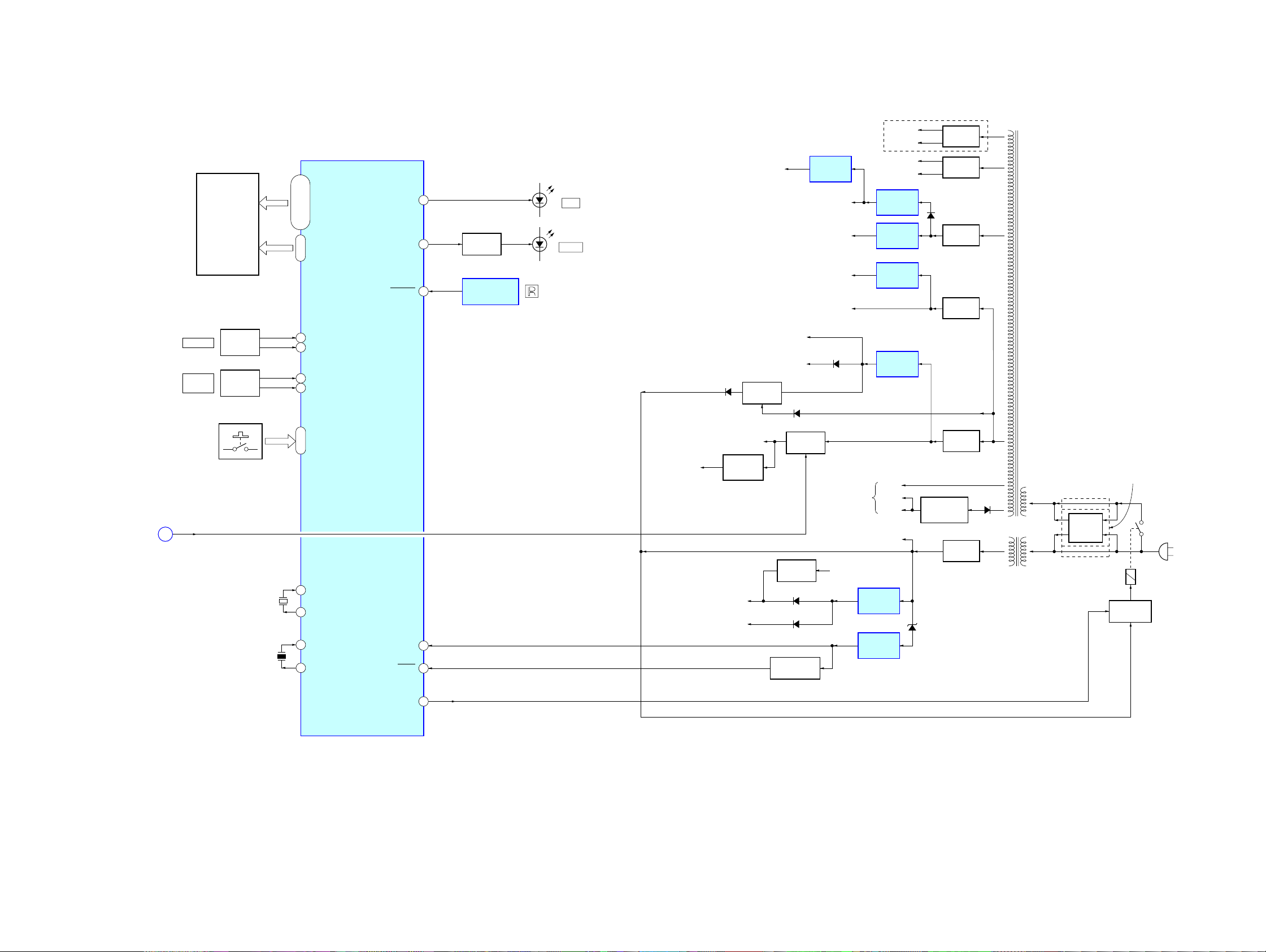
6-1. BLOCK DIAGRAM – SERVO Section –
SECTION 6
DIAGRAMS
DETECTOR
A
B
C
D
F
E
OPTICAL PICK-UP
BLOCK
(KSM-215DCP)
LASER DIODE
PD
2-AXIS
DEVICE
(TRACKING)
(FOCUS)
I-V AMP
LD
M101
(SPINDLE)
M102
(SLED)
M
M
CD +3V
AUTOMATIC
POWER
CONTROL
Q10
CH4OUTF
16
CH4OUTF
15
CH3OUTF
17
CH3OUTR
18
CH1OUTF
14
CH1OUTR
13
CH2OUTF
12
CH2OUTR
11
A
26
B
27
C
28
D
29
F
20
E
19
LD
36
MOTOR/COIL DRIVE
IC251
MOTOR
DRIVE
MOTOR
DRIVE
COIL
DRIVE
COIL
DRIVE
MUTE
20
CH4IN
CH3FIN
CH3RIN
CH1FIN
CH1RIN
CH2FIN
CH2RIN
SUMMING
FOCUS
ERROR
TRACKING
ERROR AMP
APC LD
AMP
24
23
21
4
5
5
7
RF
AMP
AMP
FILTER
CD DSP
IC101 (1/2)
AC_
SUM
34
FEO
24
TEO
22
PD
37
OPIN+
OPOUT
27
SFDR
9
SRDR
10
TFDR
11
TRDR
12
FFDR
13
FRDR
14
EQ_
IN
35
2
CD DSP
IC101 (2/2)
PWM GENERATOR
FOCUS/TRACKING/SLED
S101
(LIMIT)
RFAC
VCA
21 23
TEI
CONVERTER
FOCUS/
TRACKING/SLED
SERVO DSP
A/D
EQ
FEI
SSTP
7
RFACO
41
INTERFACE
SERVO AUTO
SEQUENCER
TO CPU INTERFACE
MIRR,
DFCT, FOK
DETECTOR
SERVO
42
45
46
RFACI
ASYI
ASYO
DIGITAL
CLV
PROCESSOR
FOK
MIRR
DFCT
COUT
119
SCLK
108
ASYMMETRY
CORRECTOR
MDP
6
100
3
1
2
XRST
51 53
FILI
PCO
FILO
CLTV
DIGITAL PLL
TO SERVO AUTO
SEQUENCER
CPU INTERFACE
DATA
CLOCK
XLAT
95
97 94
O-CD-CLK
O-CD-DATA
O-XLT (CD-LAT)
SYSTEM CONTROLLER
O-XRES (RESET)
93
1125052
XPCK
DEMODULATOR
SUBCODE
PROCESSOR
EXCK
SCOR
SENS
SBSO
SQSO
96 97
98 99115107102 105 104 110 111
I-SENS
IC601 (1/3)
O-MP3-DO
O-MP3-CLK
O-MP3 CS
I-MP3 ACK
I-MP3 REQ
I-SCOR (Q-DATA REQ)
O-MP3 LP
O-MP3 RESET
EFM
SQCK
I-MP3-DI
O-XTCN
32K
RAM
INTERNAL BUS
WFCK
XUGF
GFS
113
99
98
100
1
3
4
2
6
92
73I-CD NUM SENSER
20I-CD ENCODER
21I-CD OPEN/CLOSE
CORRECTOR
EMPH
68
MIDIO
6
MICK
7
MICS
4
MIACK
8
PO11/BUCK/AD14
36
MILP
5
RESET
2
ERROR
MP3 DECODER
IC301
LEVEL SHIFT
ROTARY
ENCODER
INTERFACE
M751
(LOADING)
M741
(TABLE)
Q731
S711
CLOSE
D/A
DIGITAL
M
M
ADDRESS DETECT
OPEN
117 93
C4M
CONVERTER
SELECTOR
LRCK
BCK
63 66 65
16
15
19
18 14
LRCKIA
SBSY/BCKIB
SFSY/LRCKIB
LOADING MOTOR DRIVE
4 OUT1
2 OUT2
TABLE MOTOR DRIVE
4 OUT1
2 OUT2
TABLE ADDRESS
SENSOR
IC731
DISC TRAY
S751
OPEN/CLOSE
DETECT
GENERATOR
D/A
PCMD
SDI0
BCKIA
CLOCK
LRCKI
BCKI
62 60 61
IC701
IC712
XTSL
XTAO
77
PCMDI
1196 5
SDO0
STANDBY
7FIN
9RIN
7FIN
9RIN
XTAI
XTACN
AOUT1
AOUT2
78
95
81
86
3
R-CH
MP3-STB
LM-F
LM-R
TM-F
TM-R
16.9344MHz
MUTING
MUTING
CONTROL
Q304, 305
• R-ch is omitted due to same as L-ch.
• SIGNAL PATH
: CD PLAY
X171
Q306
CD-MUTING
R-CH
CD
A
CD-MUTING,
MP3-STB,
LM-F, LM-R,
TM-F, TM-R
(Page 23)
(Page 23)
B
2222
6-2. BLOCK DIAGRAM – MAIN Section –
CX-JN88
FM 75Ω
COAXIAL
AM
HP1
(PB)
(DECK-A)
JK101
VIDEO/MD
(Page 22)
A
FM/AM TUNER PACK
FM ANT
ANT GND
AM ANT
ANT GND
L-CH
R-CH R-CH
L-CH
IN
L
R
CD
TUNER-L
TUNER-R
LC72121 DI
LC72121 DO
LC72121 CLK
LC72121 CE
TUNED
STEREO
TU MUTE
RDS DATA
RDS INT
R-CH
R-CH
CLK
TUNED
STEREO
TU-MUTING
RDS DATA
RDS INT
(AEP)
MD L
63
CD L
1
POWER ON
MUTING
Q105
B+9V
LINE AMP
IC102
R-CH
MUTING
Q103
MUTING
CONTROL
Q101, 102
TONE OUT1
TUNER L
61
TAPE L
DO
DI
CE
3
7
9
11
PB OUT1
TAPE A1
TAPE B1
37
INPUT SELECT,
TONE CONTROL,
ELECTRICAL VOLUME
IC101
VIN1
36
VOL OUT1
SAOUT1
AMS OUT
REC OUT1
SI
SC
19
18
33
FEED BACK
SWITCH
Q106
R-CH
56
D201
+
R-CH
40
15
IC441 (AEP, CIS)
IC441 (Chilean, Peruvian, Australian)
POWER
AMP
R-CH
STANDBY
SWITCH
Q489
R-CH
LEVEL
SHIFT
Q490, 491
POWER AMP
ON/OFF
Q308
TH441
POWER ON
MUTING
Q309, 313
THERMAL
DETECT
Q483, 484
OVER LOAD
Q441, 442
B+9V
PROTECT
Q485, 487
DETECT
+
DETECT
D481
+
DC
DETECT
Q481, 482
–1
–2
RY441
PROTECTOR
Q486, 488
+
JK441
+
–
+
–
+
–
+
–
L
FRONT SPEAKER
IMPEDANCE
USE 6 – 16Ω
R
L
SURROUND SPEAKER
IMPEDANCE
R
USE 24Ω
J801
PHONES
HRPE1
(REC/PB/ERASE)
(DECK-B)
(Page 22)
(Page 24)
R-CH R-CH
ERASE
CD-MUTING, MP3-STB,
LM-L, LM-R, TM-L, TM-R
B
FRONT SP RELAY
C
REC/PB
SWITCH
IC201,
Q322, 323
BIAS OSC
L101
TU-MUTING
CD-MUTING
LM-F
LM-R
TM-F
TM-R
MP3-STB
DI
CE
DO
CLK
TUNED
STEREO
83
86
84
67
85
O-LC72121/BU2099FV DO
68
I-TUNED-IN
I-LC72121 DI
I-STEREO-IN
O-LC72121 CE
O-LC72121/BU2099FV CLK
BIAS OSC
Q321
Q5
11
Q4
10
Q8
14
Q7
13
Q10
16
Q9
15
Q11
17
(AEP)
RDS INT
RDS DATA
7
8
I-BU1924 CLK
I-BU1924 DATA
REC BIAS
SWITCH
Q324
7
Q16Q0
DATA4CLOCK5LCH
3
LOADING/TABLE
MOTOR DRIVE
IC371
Q6
12
87
O-BU2099FV LCH
B +9V
91
88
O-BD3401 CLK
O-BD3401 DATA
AMS DETECT
Q327
69
I-AMS-IN
BAND-PASS
FILTER
Q351, 352
24
I-STREAM/VACS
SYSTEM CONTROLLER
IC601 (2/3)
19
18
I-PROTECT
WFR/HP/MIC-IN
75
O-SYSTEM-MUTE
MOTOR/PLUNGER DRIVER
IC602
MOTOR
SO
18
11
3
4
5
MP3-STB
DATA
CLOCK
LCH
SOL-A
SOL-B
I-TAPE A STAT
I-TAPE B STAT
I-REEL A IN
I-REEL B IN
8
6
7
22
23
70
71
CAPSTAN/REEL
MOTOR DRIVE
Q601
PLUNGER DRIVE
(DECK-A)
Q603
PLUNGER DRIVE
(DECK-B)
Q602
D207
TAPE MECHANISM
DECK BLOCK
CAPM+
MM
(CAPSTAN/REEL)
A-SOL
(DECK-A)
B-SOL
(DECK-B)
A-HALF
A-MODE
REC (REW)
B-HALF
B-MODE
REC (FWD)
A-PHOTO
B-PHOTO
D206
FAN MOTOR
+
DRIVE
Q310
M901
MM
(FAN)
• R-ch is omitted due to same as L-ch.
• SIGNAL PATH
: TUNER
: CD PLAY
: TAPE PLAY (DECK-A)
: TAPE PLAY (DECK-B)
: REC
: AUX IN
2323
CX-JN88
6-3. BLOCK DIAGRAM – PANEL/POWER SUPPLY Section –
(Page 23)
INDICATOR TUBE
VOLUME
AMS/
TUNING
S601 – 610,
S621 – 630,
S641 – 650
(FRONT PANEL KEYS)
FRONT SP RELAY
C
FLUORESCENT
FL601
ROTARY
ENCODER
S660
ROTARY
ENCODER
S661
X601
32.768kHz
X602
10MHz
SYSTEM CONTROLLER
S1 – 21
52 – 65
43 – 45, 47 – 50,
G1 – G13
42 – 30
9 I-VOLUME-IN1
10 I-VOLUME-IN2
81 I-MULTI-JOG IN1
82 I-MULTI-JOG IN2
I-KEY1 –
I-KEY3
27 – 25
I-XT1
1312O-XT2
15
CF1
CF2
16
IC601 (3/3)
O-POWER LED
O-I-BASS LED
I-SIRCS-IN
(E51, AUS)
AMP B+ 2
AMP B– 2
REGULATOR
REGULATOR
REGULATOR
REGULATOR
VF1, 2
–VFL
EVER +10V
+3.3V
REGULATOR
IC603
VOLTAGE
DETECT
IC604
AMP B+ 1
AMP B– 1
+3.3V
IC302
+3.3V
IC301
+9V
IC303
+9V
IC304
VP
+1.5V
M +9V
D321
B+ SWITCH
Q312
B+ SWITCH
Q604, 616
D609
D607, 608
Q605
REGULATOR
IC303
CD +3V
B+3.5V
B+9V
UNREG +16V
D324 – 326
TO
FLUORESCENT
INDICATOR TUBE
B+3.5V
CD +1.5V
76
77
28
29I-AC CUT
11RESET
LED DRIVE
Q609
REMOTE CONTROL
RECEIVER
IC610
LED601
I/1
LED602
i-BASS
FAN B+
D316
+12V
REGULATOR
Q311
VDD2
VDD1,
VDD3/4
B+ SWITCH
Q314, 315
RY B+
CD M+7V
RESET SWITCH
D314, 315
–27V
REGULATOR
Q902
D610
RECT
D402
RECT
D401
RECT
D301 – 304
RECT
D305 – 308
RECT
D309 – 312
RECT
D902 – 904
MAIN POWER
TRANSFORMER
D908
RECT
SUB POWER
TRANSFORMER
PT901
PT902
• Abbreviation
AUS: Australian models
E51 : Chilean and Peruvian models
(E51)
(EXCEPT E51)
VOLTAGE
SELECTOR
S901
(EXCEPT E51)
RY901
RELAY DRIVE
Q361, 362
W001
(AC IN)
74O-POWER RELAY
2424
CX-JN88
d
• Note for Printed Wiring Boards and Schematic Diagrams
Note on Printed Wiring Board:
• X : parts extracted from the component side.
• Y : parts extracted from the conductor side.
• : Pattern from the side which enables seeing.
(The other layers' patterns are not indicated.)
Caution:
Pattern face side: Parts on the pattern face side seen from
(Conductor Side) the pattern face are indicated.
Parts face side: Parts on the parts face side seen from
(Component Side) the parts face are indicated.
• Indication of transistor
C
B
Q
B
E
Q
CE
These are omitted.
These are omitted.
Note on Schematic Diagram:
• All capacitors are in µF unless otherwise noted. (p: pF)
50 WV or less are not indicated except for electrolytics
and tantalums.
• All resistors are in Ω and 1/
specified.
• f : internal component.
• 2 : nonflammable resistor.
• 5 : fusible resistor.
• C : panel designation.
Note: The components identified by mark 0 or dotted line
with mark 0 are critical for safety.
Replace only with part number specified.
• A : B+ Line.
• B : B– Line.
• Voltages and waveforms are dc with respect to ground
under no-signal conditions.
– CD Board –
no mark : CD PLAY
– Other Sections –
no mark : FM
(): TAPE PLAY
〈〈 〉〉 : TAPE REC
[]: CD PLAY
∗ : Impossible to measure
• Voltages are taken with a V OM (Input impedance 10 MW).
Voltage variations may be noted due to normal production tolerances.
• Waveforms are taken with a oscilloscope.
Voltage variations may be noted due to normal production tolerances.
• Circled numbers refer to waveforms.
• Signal path.
F : TUNER (FM/AM)
E : TAPE PLAY (DECK A)
d : TAPE PLAY (DECK B)
G : REC
J : CD PLAY
L : AUX IN
• Abbreviation
AUS: Australian model
E51 : Chilean and Peruvian models
4
W or less unless otherwise
• Circuit Boards Location
PANEL board
HEADPHONE board
MOTOR (LD) board
TRANS board
TRANSLATION board
(AEP, CIS)
SW board
SUB TRANS board
CDMP3 CONNECT board
MAIN boar
POWER board
SENSOR board
CD board
MOTOR (TB) board
2525
Loading...