

Page 1

SERVICE MANUAL
AC Power Source/Analyzer
Agilent Models 6814B and 6834B
Regulatory Test Solution (RTS) - formerly called
the Harmonic/Flicker Test System (HFTS)
Agilent Model 6843A
For instruments with Serial Numbers:
Model 6814B: 3601A-00101 through 00272
US36010273 and up
Model 6834B: 3601A-00101 through 00403
US36010404 and up
Model 6843A: 3531A-00101 through 00256
US35310257 and up
Agilent Part No. 5962-0891 Printed in USA
Microfiche Part No. 5962-0892 October, 2000
Page 2

CERTIFICATION
Agilent Technologies certifies that this product met its published specifications at time of shipment from the factory. Agilent
Technologies further certifies that its calibration measurements are traceable to the United States National Bureau of
Standards, to the extent allowed by the Bureau's calibration facility, and to the calibration facilities of other International
Standards Organization members.
WARRANTY
This Agilent Technologies hardware product is warranted against defects in material and workmanship for a period of three
years from date of delivery. Agilent Technologies software and firmware products, which are designated by Agilent
Technologies for use with a hardware product and when properly installed on that hardware product, are warranted not to
fail to execute their programming instructions due to defects in material and workmanship for a period of 90 days from date
of delivery. During the warranty period Agilent Technologies will, at its option, either repair or replace products which
prove to be defective. Agilent Technologies does not warrant that the operation of the software, firmware, or hardware shall
be uninterrupted or error free.
For warranty service, with the exception of warranty options, this product must be returned to a service facility designated
by Agilent Technologies. Customer shall prepay shipping charges by (and shall pay all duty and taxes) for products returned
to Agilent Technologies for warranty service. Except for products returned to Customer from another country, Agilent
Technologies shall pay for return of products to Customer.
Warranty services outside the country of initial purchase are included in Agilent Technologies's product price, only if
Customer pays Agilent Technologies international prices (defined as destination local currency price, or U.S. or Geneva
Export price).
If Agilent Technologies is unable, within a reasonable time to repair or replace any product to condition as warranted, the
Customer shall be entitled to a refund of the purchase price upon return of the product to Agilent Technologies.
LIMITATION OF WARRANTY
The foregoing warranty shall not apply to defects resulting from improper or inadequate maintenance by the Customer,
Customer-supplied software or interfacing, unauthorized modification or misuse, operation outside of the environmental
specifications for the product, or improper site preparation and maintenance. NO OTHER WARRANTY IS EXPRESSED
OR IMPLIED. AGILENT TECHNOLOGIES SPECIFICALLY DISCLAIMS THE IMPLIED WARRANTIES OF
MERCHANTABILITY AND FITNESS FOR A PARTICULAR PURPOSE.
EXCLUSIVE REMEDIES
THE REMEDIES PROVIDED HEREIN ARE THE CUSTOMER'S SOLE AND EXCLUSIVE REMEDIES. AGILENT
TECHNOLOGIES SHALL NOT BE LIABLE FOR ANY DIRECT, INDIRECT, SPECIAL, INCIDENTAL, OR
CONSEQUENTIAL DAMAGES, WHETHER BASED ON CONTRACT, TORT, OR ANY OTHER LEGAL THEORY.
ASSISTANCE
The above statements apply only to the standard product warranty. Warranty options, extended support contracts, product
maintenance agreements and customer assistance agreements are also available. Contact your nearest Agilent
Technologies Sales and Service office for further information on Agilent Technologies's full line of Support Programs.
2
Page 3
SAFETY CONSIDERATIONS
GENERAL. This is a Safety Class 1 instrument (provided with terminal for connection to protective earth ground).
OPERATION. BEFORE APPLYING POWER verify that the product is set to match the available line voltage, the correct
line fuse is installed, and all safety precautions (see following warnings) are taken. In addition, note the instrument's external
markings described under "Safety Symbols".
WARNING.
• Servicing instructions are for use by service-trained personnel. To avoid dangerous electrical shock, do not perform any
servicing unless you are qualified to do so.
• BEFORE SWITCHING ON THE INSTRUMENT, the protective earth terminal of the instrument must be connected to
the protective conductor of the (mains) power cord. The mains plug shall be inserted only in an outlet socket that is
provided with a protective earth contact. This protective action must not be negated by the use of an extension cord
(power cable) that is without a protective conductor (grounding). Grounding one conductor of a two-conductor outlet is
not sufficient protection.
• If this instrument is to be energized via an auto-transformer (for voltage change), make sure the common terminal is
connected to the earth terminal of the power source.
• Any interruption of the protective (grounding) conductor (inside or outside the instrument), or disconnecting of the
protective earth terminal will cause a potential shock hazard that could result in personal injury.
• Whenever it is likely that the protective earth connection has been impaired, this instrument must be made inoperative
and be secured against any unintended operation.
• Only fuses with the required rated current, voltage, and specified type (normal blow, time delay, etc.) should be used.
Do not use repaired fuses or short-circuited fuseholders. To do so could cause a shock or fire hazard.
• Do not operate this instrument in the presence of flammable gases or fumes.
• Do not install substitute parts or perform any unauthorized modification to this instrument.
• Some procedures described in this manual are performed with power supplied to the instrument while its protective
covers are removed. If contacted, the energy available at many points may result in personal injury.
• Any adjustment, maintenance, and repair of this instrument while it is opened and under voltage should be avoided as
much as possible. When this is unavoidable, such adjustment, maintenance, and repair should be carried out only by a
skilled person who is aware of the hazard involved.
• Capacitors inside this instrument may hold a hazardous electrical charge even if the instrument has been disconnected
from its power source.
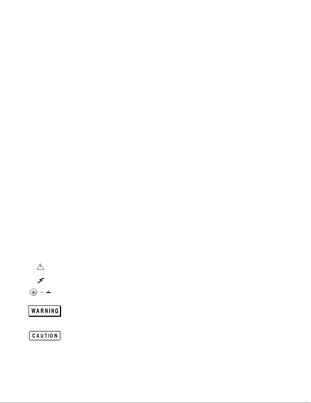
SAFETY SYMBOLS.
Instruction manual symbol. The instrument will be marked with this symbol when it is necessary for you to refer to the
instruction manual in order to protect against damage to the instrument.
This sign indicates hazardous voltages.
This sign indicates an earth terminal (sometimes used in the manual to indicate circuit common connected to a ground
chassis).
The WARNING sign denotes a hazard. It calls attention to a procedure, practice, or the like, which, if not correctly
performed or adhered to, could result in personal injury. Do not proceed beyond a WARNING sign until the
indicated conditions are fully understood and met.
The CAUTION sign denotes a hazard. It calls attention to an operating procedure, or the like, which, if not correctly
performed or adhered to, could result in damage to or destruction of part or all of the product. Do not proceed
beyond a CAUTION sign until the indicated conditions are fully understood and met.
.
3
Page 4

Printing History
The current edition of this manual is indicated below. Reprints of this manual containing minor corrections and updates
may have the same printing date. Revised editions are identified by a new printing date. A revised edition incorporates all
new or corrected material since the previous printing date.
Changes to the manual occurring between revisions are covered by change sheets shipped with the manual. In some cases,
the manual change applies only to specific instruments. Instructions provided on the change sheet will indicate if a particular
change applies only to certain instruments.
This document contains proprietary information protected by copyright. All rights are reserved. No part of this document
may be photocopied, reproduced, or translated into another language without the prior consent of Agilent Technologies. The
information contained in this document is subject to change without notice.
Instrument Identification
The power supply is identified by a unique, two-part serial number, such as, 3601A-00101. The items in this serial number
are explained as follows:
Item Description
US The letter suffix indicates the country of manufacture, where US = USA.
3601 This is a code that identifies either the date of manufacture, or the date of a significant design change.
0101 The last five digits of the serial number (0101) is a unique number assigned to each AC Power Source.
Copyright 1996 Agilent Technologies Company Edition 1____________________September, 1996
Update 1_______________________ January 1999
Update 2_______________________ October 2000
4
Page 5

Table of Contents
1. Introduction
Scope ............................................................................................................................................................7
Organization ..............................................................................................................................................7
Safety Considerations...................................................................................................................................7
Related Documents....................................................................................................................................7
Revisions ......................................................................................................................................................7
Manual Revisions......................................................................................................................................7
Firmware Revisions ...................................................................................................................................8
Electrostatic Discharge.................................................................................................................................8
2. Performance Tests
Introduction ..................................................................................................................................................9
Test Equipment Required.............................................................................................................................9
General Measurement Techniques................................................................................................................9
Current-Monitoring Resistor ......................................................................................................................10
Performance Tests ......................................................................................................................................10
Performance Test Record Sheets................................................................................................................10
3. Troubleshooting
Introduction ................................................................................................................................................19
Localizing the Problem...............................................................................................................................19
Test Equipment Required...........................................................................................................................19
List of Equipment .......................................................................................................................................19
Troubleshooting Procedure ........................................................................................................................19
Using the *TST? Query..............................................................................................................................19
Firmware Revisions ....................................................................................................................................20
ROM Replacement or ROM Update ..........................................................................................................20
Calibration Configuration Switch ...............................................................................................................21
Troubleshooting Hints................................................................................................................................22
Switching Amplifier Output Balancing......................................................................................................22
4. Principles of Operation
Introduction ................................................................................................................................................31
General Description....................................................................................................................................31
A1, A2, A3 Switching Amplifier Modules .................................................................................................31
A4 Mother Board Assembly .......................................................................................................................31
A5 Relay Range / Sense Assembly.............................................................................................................32
A6 Servo (Control) Assembly ....................................................................................................................32
A7 IEEE-488 (GPIB) / RS-232 Interface Assembly ..................................................................................32
A8 Digital Signal Processing Assembly .....................................................................................................32
A9 Input Power Assembly (208 Volt Input)...............................................................................................32
A9 Input Power Assembly (400 Volt Input)...............................................................................................32
A10 Auxiliary Power Supply......................................................................................................................33
A11 Front Panel Display Assembly............................................................................................................33
A12 Input Filter Assembly .........................................................................................................................33
A13 Bridge Capacitor Filter Assembly.......................................................................................................33
A14 Bias Power Supply..............................................................................................................................33
5. Replaceable Parts
Introduction ................................................................................................................................................35
5
Page 6

Table of Contents (continued)
6. Diagrams
Introduction ................................................................................................................................................37
General Schematic Notes............................................................................................................................37
Index...............................................................................................................................................53
Figures
2-1. Verification Test Setup.................................................................................................................................... 17
2-2. Verification Test Setup.....................................................................................................................................18
3-1. Bias Voltage to Switching Amplifier Assemblies.............................................................................................28
3-2. AC Programming Signal Path ..........................................................................................................................29
4-1. Agilent Series 665xA/667xA Power Supply, Block Diagram ..........................................................................34
6-1. Mechanical Layouts..........................................................................................................................................38
6-2. Agilent 6814B, 6834B, 6843A Front Frame Assembly....................................................................................39
6-3. A9 208/230V AC Input Board Parts Location .................................................................................................40
6-4. A9 208/230V AC Input Assembly Schematic ..................................................................................................41
6-5. A9 400V AC Input Board Parts Location.........................................................................................................42
6-6. A9 400V AC Input Assembly Schematic .........................................................................................................43
6-7. A10 Auxiliary Power Supply Board Parts Location.........................................................................................44
6-8. A10 Auxiliary Power Supply Assembly Schematic..........................................................................................45
6-9. A14 Bias Power Supply Board Parts Location.................................................................................................46
6-10. A14 Bias Power Supply Assembly Schematic.................................................................................................47
6-11. A5 Range/Output/Phase Relay Schematic.......................................................................................................48
6-12. A5 Range/Output/Phase Relay Driver Schematic............................................................................................49
6-13. A4 Mother Board Parts Location.....................................................................................................................50
6-14. A8 DSP Board Parts Location.........................................................................................................................51
6-15. A6 Servo Board Test Point Locations.............................................................................................................52
Tables
2-1. Test Equipment Required .....................................................................................................................................9
2-2. Performance Tests ..............................................................................................................................................10
2-3. Performance Test Record Form...........................................................................................................................13
2-4. Performance Test Record Agilent 6814B............................................................................................................14
2-4. Performance Test Record Agilent 6834B............................................................................................................15
2-4. Performance Test Record Agilent 6843A............................................................................................................16
3-1. Test Equipment Requirements for Troubleshooting............................................................................................19
3-2. Specific Troubleshooting Procedures..................................................................................................................21
3-3. AC Power Source Troubleshooting Procedure ....................................................................................................23
3-4. A9 208/208 Input Power Supply Troubleshooting..............................................................................................25
3-5. A9 Option 400 (400V) AC Input Power Supply Troubleshooting ......................................................................25
3-6. A10 Auxiliary Power Supply Troubleshooting....................................................................................................26
3-7. Al4 Option 400 Bias Power Supply Troubleshooting .........................................................................................26
3-8. A4 Mother Board Troubleshooting .....................................................................................................................27
3-9. A5 Mother Board Troubleshooting .....................................................................................................................27
5-1. Agilent 68l4B, 6834B, 6843A Replacement .......................................................................................................35
6-1. General Schematic Notes.....................................................................................................................................37
6
Page 7
Introduction
Scope
Organization
This manual contains information for troubleshooting and repairing to the component level Agilent Model 6814B, 6834B
AC Power Source/Analyzers and Agilent Model 6843A Regulatory Test Solution, hereafter referred to as an AC Power
Source. The manual applies to both standard units and units that have Option 400. This manual is organized as follows:
Chapter Description
Chapter 2 Performance tests
Chapter 3 Troubleshooting procedures
Chapter 4 Principles of operation on a block-diagram level
Chapter 5 Replaceable parts
Chapter 6 Diagrams
Safety Considerations
This AC Power Source is a Safety Class I instrument, which means it has a protective earth terminal. This terminal must be
connected to earth ground through a power source equipped with a 4-wire, ground receptacle. Refer to the “Safety
Summary” page at the beginning of this manual for general safety information. Before operation or repair, check the AC
Power Source and review this manual for safety warnings and instructions. Safety warnings for specific procedures are
located at appropriate places in the manual.
Hazardous voltages exist within the AC Power Source chassis, at the output terminals, and at the analog
Related Documents
The following documents are shipped with your ac source:
• Quick Start Guide, to help you quickly get started using the ac source.
• User's Guide, containing detailed installation, checkout, and front panel information.
• Programming Guide, containing detailed GPIB programming information.
• Quick Reference Card, designed as a memory jogger for the experienced user.
programming terminals.
1
Revisions
Manual Revisions
This manual was written for AC Power Sources; that have the same serial prefixes (first part) as those listed on the title page
and whose serial numbers (second part) are equal to or higher than those listed in the title page.
Introduction
7
Page 8
Note 1) If the serial prefix of your unit is higher than that shown in the title page then the unit was made after
the publication of this manual and may have hardware and/or firmware differences not covered in this
manual. If they are significant to the operation and/or servicing of the AC Power Source, those differences
are documented in one or more Manual Change sheets included with this manual.
2) If the serial prefix on the unit; is lower than that shown on the title page, then the unit was made before
the publication of this manual and can be different from that described here. Such differences are covered
in “Appendix A - Manual Backdating Changes” in the User’s Manual.
Firmware Revisions
You can obtain the firmware revision number by either reading the integrated circuit label, or query the AC Power Source;
using the GPIB *IDN query command (see "Chapter 3 -Troubleshooting" ).
Electrostatic Discharge
The power supply has components that can be damaged by ESD (electrostatic discharge). Failure to
observe standard, antistatic practices can result in serious degradation of performance, even when an
actual failure does not occur.
When working on the AC Power Source; observe all standard, antistatic work practices. These include, but are not limited
to:
• working at a static-free station such as a table covered with static-dissipative laminate or with a conductive table mat
(Agilent P/N 9300-0797, or equivalent).
• using a conductive wrist strap, such as Agilent P/N 9300-0969 or 9300-0970.
• grounding all metal equipment at the station to a single common ground.
• connecting low-impedance test equipment to static-sensitive components only when those components have power
applied to them.
• removing power from the AC Power Source before removing or installing printed circuit boards .
8
Introduction
Page 9
Performance Tests
Introduction
This chapter provides test procedures for checking the operation of an Agilent Model 6814B/6834B AC Power
Source/Analyzer or Agilent Model 6843A RTS. The required test equipment is specified and sample performance test
record sheets are included. Instructions are given for performing the tests using the front panel keypad.
Test Equipment Required
Table 2-1 lists the equipment required to perform the verification tests given in this chapter.
Table 2-1. Test Equipment Required
Equipment Characteristics Recommended Model
Digital Voltmeter* Resolution: 10nV @ 1V
Readout: 81/2 digits
Accuracy: <20ppm
Current Monitor 0.01 ohms +/-200ppm 10W Guildline 7320/0.01
Agilent 3458A
2
Audio Analyzer Input Voltage Range: 50mV to 300 V
Distortion Accuracy: +/-1 db 20Hz to 20KHz
Residual Distortion / Noise: -80db (0.0 1 %) 20Hz to 20KHz
Frequency Counter Accuracy @ 1 KHz < 0.001% Agilent5316B
Ratio Transformer* 30:1 ratio < 50ppm
Variable –Voltage
Transformer
Load Resistors 6814B use 4 ea. 7.5 ohms > 1000W
GPIB Controller Full GPIB capabilities HP Series 200/300
* The 30:1 ratio transformer is not required for a valid MIL-STD 45662A test. The 30:1 ratio transformer is only required when a 4:1
test equipment to specification ratio is desired using a 3458A voltmeter in the 1000 volt range.
Power: 3 phase 24 KVA
Range: 180-254V 47-63 Hz
360-440V 47-63 Hz
6834B use 4 ea. 15 ohm > 1000W
6843A use 4 ea. 5 ohm > 1500W
Agilent8903A
Superior Powerstat
1156DT-3Y
0-280 50A 24.2KVA
or equivalent
General Measurement Techniques
The following chapters provide the test procedures for verifying the Agilent 6814B, 6834B or 6843A's compliance with the
specifications listed in Appendix A of the Users Guide. Please refer to CALIBRATION PROCEDURE or
TROUBLESHOOTING if you observe out-of specification performance. The performance test specifications are listed in
the Performance Test Record Card at the end of this chapter. You can record the actual measured values in the columns
Performance Tests
9
Page 10
provided. Select an adequate gauge wire for load tests using the procedures given in the operating manual for connecting
the load.
Current-Monitoring Resistor
To eliminate output current measurement error caused by voltage drops in the leads and connections, connect the
current-monitoring resistor as a four terminal device.
Performance Tests
Performance tests check all the specifications of the ac source. The various tests are grouped under Table 2-2. If more than
one meter or a meter and an oscilloscope are used, connect each to the sense terminals by separate leads to avoid mutual
coupling effects.
Performance Test Record Sheets
When performing the tests in this chapter, refer to the Performance Test Record sheets ( Table 2-3 and Table 2-4 ) at the
end of this chapter. Table 2-3 is for recording common information, such as test equipment used and environmental
conditions. Table 2-4 is for recording the actual measurements.
Table 2-2. Voltage / Frequency Programming and Readback Accuracy
Step Action Normal Result
This procedure verifies that the voltage programming and GPIB readback and front panel display functions are within
specifications.
1
2
3
4
5
6
7
Turn off ac source. Connect DVM and Ratio Transformer if
used across output terminals as shown in Test Setup Figure 2-1.
Turn on ac source with no load. Press [Shift] [Output], display
reads *RST, press [Enter].
Program VOLT:ALC EXT, VOLT 300, FREQ 45, CURR 10
Enable output press [Output on/off].
Record output voltage / frequency measurements from DVM /
front panel and frequency meter.
Program FREQ 400.
Record output voltage / frequency measurements from DVM /
front panel and frequency meter.
Program FREQ 1000.
*RST resets ac source to known factory
state.
CV annunciator on.
Output voltage at 300 volts.
Output voltage / frequency measurements
within specified limits on test card.
Output voltage / frequency measurements
within specified limits on test card.
8
9
10
11
12
13
14
10
Performance Tests
Record output voltage / frequency measurements from DVM /
front panel and frequency meter.
Program VOLT:RANGE 150, VOLT 150, FREQ 45.
Record output voltage / frequency measurements from DVM /
front panel and frequency meter.
Program FREQ 400.
Record output voltage / frequency measurements from DVM /
front panel and frequency meter.
Program FREQ 1000.
Record output voltage / frequency measurements from DVM /
front panel and frequency meter.
Output voltage / frequency measurements
within specified limits on test card.
CV annunciator on.
Output voltage at 150 volts.
Output voltage / frequency measurements
within specified limits on test card.
Output voltage / frequency measurements
within specified limits on test card.
Output voltage / frequency measurements
within specified limits on test card.
Page 11
Table 2-2. ( Continued ) CV Load Effect
Step Action Normal Result
This test measures the change in output voltage resulting from a change in output current from full-load to no-load or
no-load to full-load.
1
2
3
4
5
6
7
Turn off ac source. Connect DVM across output terminals ( or
ratio transformer if used ) and 7.5 ohm for Agilent 6814B, 15
ohm for 6834B or 5 ohms for 6843A load resistors as shown in
Test Setup Figure 2-1.
Turn on ac source. Press [Shift] [Output] display reads *RST
press [Enter].
Program VOLT:ACL EXT, VOLT:RANGE 150 VOLT 150
CURR 20 for Agilent 6814B, CURR 10 for Agilent 6834B or
CURR 32 for Agilent6843A. Enable output press [Output
on/off].
Record output voltage measurement from DVM.
Open S1 ( S2 or S3 if Agilent 6834B ). Output current near zero.
Record output voltage measurement from DVM.
Check test result.
*RST resets ac source to known factory
default state.
CV annunciator on or reduce voltage until
CV annunciator come on.
Output current near 20A for
Agilent6814B, 10A for Agilent 6834B or
30A for Agilent6843A.
The difference between the DVM
readings in step 4 & 6 are within the
specified load effect limits.
Table 2-2. ( Continued ) CV Source Effect
Step Action Normal Result
This test measures the change in output voltage resulting from a change in ac mains input voltage from the minimum to
maximum value within the line voltage specification.
1
2
3
4
5
6
Turn off ac source. Connect DVM across output terminals ( or
ratio transformer if used ) and 30 ohm for Agilent 6814B, 60
ohm for 6834B or 20 ohm for Agilent6843A load resistors as
shown in Test Setup Figure 2-1.
Turn on ac source. Press [Shift] [Output] display reads *RST
press [Enter].
Program VOLT:ALC EXT, VOLT 300, CURR 10 for Agilent
6814B, CURR 5 for Agilent 6834B or CURR 16 for
Agilent6843A.
Enable output press [Output on/off].
Adjust the variable transformer to low line condition. ( 180 or
360 Vac ).
Record voltage reading of DMM.
Adjust the variable transformer to high line condition. ( 254 or
440 Vac ).
Record voltage reading of DMM.
Check test result.
*RST resets ac source to known factory
default state.
CV annunciator on or reduce voltage until
CV annunciator comes on.
Output current near 10A for
Agilent6814B;
5A for Agilent 6834B or 15A for
Agilent6843A.
The difference between the DVM
readings in step 3 & 5 are within the
specified load effect limits.
Performance Tests
11
Page 12
Table 2-2. ( Continued ) rms Current Accuracy Test
Step Action Normal Result
This test verifies the measurement accuracy of the rms current readback.
1
2
3
4
Step Action Normal Result
1
2
3
4
Turn off ac source. Connect Current Shunt, 7.5 ohm for Agilent
6814B, 15 ohm for Agilent 6834B or 5 ohm for Agilent6843A
load resistors and DVM as shown in Test Setup Figure 2- 2.
Turn on ac source. Press [Shift] [Output] display reads *RST
press [Enter].
Program VOLT 100, CURR 10 for Agilent 6814B, CURR 5
for Agilent6834B or CURR 15 for Agilent6843A.
Enable output press [Output on/off].
Record DMM reading and calculate rms current.
Record front panel reading.
Table 2-2. ( Continued ) Harmonic Distortion Test
This test measures the total harmonic distortion of the output sinewave at full power.
Turn off ac source. Connect Audio Analyzer across output
terminals (or ratio transformer if used) and 7.5 ohm for Agilent
6814B, 15 ohm for Agilent 6834B or 5 ohms for Agilent6843A
load resistors as shown in Test Setup Figure 2-1 .
Turn on ac source. Press [Shift] [Output] display reads *RST
press [Enter].
Program output voltage to VOLT:RANGE 150, VOLT 150,
CURR 20 for Agilent6814B, CURR 10 for Agilent 6834B or
CURR 32 for Agilent6843A.
Record the total harmonic distortion reading from the audio
analyzer and front panel display.
*RST resets ac source to known factory
default state.
CC annunciator on or increase voltage till
CC annuniciator comes on.
Output current near 10A for Agilent6814B;
5A for Agilent 6834B or 15A for
Agilent6843A.
Difference between measured output
current and front panel current reading is
within specified limits.
*RST resets ac source to known factory
default state.
CV annunciator on or reduce voltage until
CV annunciator comes on. Output
current near 20A for Agilent6814B, 10A
for Agilent6834B or 30A for
Agilent6843A
Readings are less than maximum
specified limits.
12
Performance Tests
Page 13

Table 2-3 Performance Test Record Form
Test Facility:
__________________________________________ Report No.__________________________________________
__________________________________________ Date______________________________________________
__________________________________________ Customer___________________________________________
__________________________________________ Tested By___________________________________________
Model_____________________________________ Ambient Temperature
_________________________________________________
Serial No.__________________________________ Relative Humidty
______________________________________ __________
Options__________________________________ Nominal Line Frequency
(Hz) __________________________________ __________
Firmware Revision ___________________________
Special Notes:
____________________________________________________________________________________________
____________________________________________________________________________________________
____________________________________________________________________________________________
____________________________________________________________________________________________
____________________________________________________________________________________________
____________________________________________________________________________________________
Test Equipment Used
Description Model No. Trace No. Cal. Due Date
1. Digital Voltmeter ________ ___________ ___________
2. Frequency Meter ________ ___________ ___________
3. Audio Meter ________ ___________ ___________
4. Ratio Transformer ________ ___________ ___________
5. ________ ___________ ___________
Performance Tests
13
Page 14
Table 2-4. Performance Test Record - Agilent 6814B AC Power Source
Model: Agilent 6814B Report No.: Date:
Test Description Min Spec Results Max Spec Meas
Voltage Programming & Readback Accuracy
High Range@ 45 Hertz
Program 300V
Front Panel Display
299.250
Vrms-400mV
High Range@ 400 Hertz
Program 300V
Front Panel Display
298.200
Vrms-400mV
High Range@ 1000 Hertz
Program 300V
Front Panel Display
296.700
Vrms-400mV
Low Range@ 45 Hertz
Program 150V
Front Panel Display
149.475
Vrms-325mV
Low Range@ 400 Hertz
Program 150V
Front Panel Display
148.950
Vrms-325mV
______V
______V
______V
______V
______V
______V
______V
______V
______V
______V
300.750
Vrms+400mV
301.800
Vrms+400mV
303.300
Vrms+400mV
150.525
Vrms+325mV
151.050
Vrms+325mV
Uncert **
140mV
( 1.2mV )
140mV
( 1.2mV )
140mV
( 1.2mV )
70mV
( 0.6mV )
70mV
( 0.6mV )
Low Range@ 1000 Hertz
Program 150V
Front Panel Display
148.200
Vrms-325mV
______V
______V
151.800
Vrms+325mV
70mV
( 0.6mV )
CV Load Effect Vo-0.75V ______V Vo+0.75V
CV Line Effect Vo-0.3V ______V Vo+0.3V
Rms Current Readback Io-0.060A ______A Io+0.060A l.lmA
Total Harmonic Distortion
Audio Analyzer
Front Panel Display
0%
0%
______%
______%
1%
1%
Frequency Programming & Readback Accuracy
Program 45Hz 44.985 ______Hz 45.014 0.9mHz
Front Panel Display Fo-0.014Hz ______Hz Fo+0.014Hz
Program 1 KHz 999.89 ______Hz 1000.110 0.010Hz
Front Panel Display Fo-0.110Hz ______Hz Fo+0.110Hz
**Note: 1. Measurement uncertainties are only valid when using test equipment listed in Table 2-1.
2. Voltage Programming and Readback measurements uncertainties are for a 3458A DMM in the 1000 volt range.
3. Measurement uncertainties in parenthesis are only if a 30:1 ratio transformer is used with the 3458A DMM.
14
Performance Tests
Page 15
Table 2-4. (Continued) Performance Test Record – Agilent 6834B AC Power Source
Model: Agilent 6843B Report No.: Date:
Test Description Min Spec Results Max Spec Meas
Voltage Programming & Readback Accuracy
High Range@ 45 Hertz
Program 300V
Front Panel Display
299.250
Vrms-400mV
High Range@ 400 Hertz
Program 300V
Front Panel Display
298.200
Vrms-400mV
High Range@ 1000 Hertz
Program 300V
Front Panel Display
296.700
Vrms-400mV
Low Range@ 45 Hertz
Program 150V
Front Panel Display
149.475
Vrms-325mV
Low Range@ 400 Hertz
Program 150V
Front Panel Display
148.950
Vrms-325mV
______V
______V
______V
______V
______V
______V
______V
______V
______V
______V
300.750
Vrms+400mV
301.800
Vrms+400mV
303.300
Vrms+400mV
150.525
Vrms+325mV
151.050
Vrms+325mV
Uncert **
140mV
( 1.2mV )
140mV
( 1.2mV )
140mV
( 1.2mV )
70mv
( 0.6mV )
70mV
( 0.6mV )
Low Range@ 1000 Hertz
Program 150V
Front Panel Display
148.200
Vrms-325mV
______V
______V
151.800
Vrms+325mV
70mV
( 0.6mV )
CV Load Effect Vo-0.75V ______V Vo+0.75V
CV Line Effect Vo-0.3V ______V Vo+0.3V
rms Current Readback Io-0.030A ______A Io+0.030A l.lmA
Total Harmonic Distortion
Audio Analyzer
Front Panel Display
0%
0%
______%
______%
1%
1%
Frequency Programming & Readback Accuracy
Program 45Hz 44.985 ______Hz 45.014 0.9mHz
Front Panel Display Fo-0.014Hz ______Hz Fo+0.014Hz
Program 1 KHz 999.89 ______Hz 1000.110 0.010Hz
Front Panel Display Fo-0.110Hz ______Hz Fo+0.110Hz
**Note: 1. Measurement uncertainties are only valid when using test equipment listed in Table 2-1.
2. Voltage Programming and Readback measurements uncertainties are for a 3458A DMM in the 1000 volt range.
3. Measurement uncertainties in parenthesis are only if a 30:1 ratio transformer is used with the 3458A DMM
Performance Tests
15
Page 16

Table 2-4. Performance Test Record - Agilent 6843A AC Power Source
Model: Agilent 6843A Report No.: Date:
Test Description Min Spec Results Max Spec Meas
Voltage Programming & Readback Accuracy
High Range@ 45 Hertz
Program 300V
Front Panel Display
299.250
Vrms-400mV
High Range@ 400 Hertz
Program 300V
Front Panel Display
298.200
Vrms-400mV
High Range@ 1000 Hertz
Program 300V
Front Panel Display
296.700
Vrms-400mV
Low Range@ 45 Hertz
Program 150V
Front Panel Display
149.475
Vrms-325mV
Low Range@ 400 Hertz
Program 150V
Front Panel Display
148.950
Vrms-325mV
______V
______V
______V
______V
______V
______V
______V
______V
______V
______V
300.750
Vrms+400mV
301.800
Vrms+400mV
303.300
Vrms+400mV
150.525
Vrms+325mV
151.050
Vrms+325mV
Uncert **
140mV
( 1.2mV )
140mV
( 1.2mV )
140mV
( 1.2mV )
70mV
( 0.6mV )
70mV
( 0.6mV )
Low Range@ 1000 Hertz
Program 150V
Front Panel Display
148.200
Vrms-325mV
______V
______V
151.800
Vrms+325mV
70mV
( 0.6mV )
CV Load Effect Vo-0.75V ______V Vo+0.75V
CV Line Effect Vo-0.3V ______V Vo+0.3V
Rms Current Readback Io-0.090A ______A Io+0.090A l.lmA
Total Harmonic Distortion
Audio Analyzer
Front Panel Display
0%
0%
______%
______%
1%
1%
Frequency Programming & Readback Accuracy
Program 45Hz 44.985 ______Hz 45.014 0.9mHz
Front Panel Display Fo-0.014Hz ______Hz Fo+0.014Hz
Program 1 KHz 999.89 ______Hz 1000.110 0.010Hz
Front Panel Display Fo-0.110Hz ______Hz Fo+0.110Hz
**Note: 1. Measurement uncertainties are only valid when using test equipment listed in Table 2-1.
2. Voltage Programming and Readback measurements uncertainties are for a 3458A DMM in the 1000 volt range.
3. Measurement uncertainties in parenthesis are only if a 30:1 ratio transformer is used with the 3458A DMM.
16
Performance Tests
Page 17
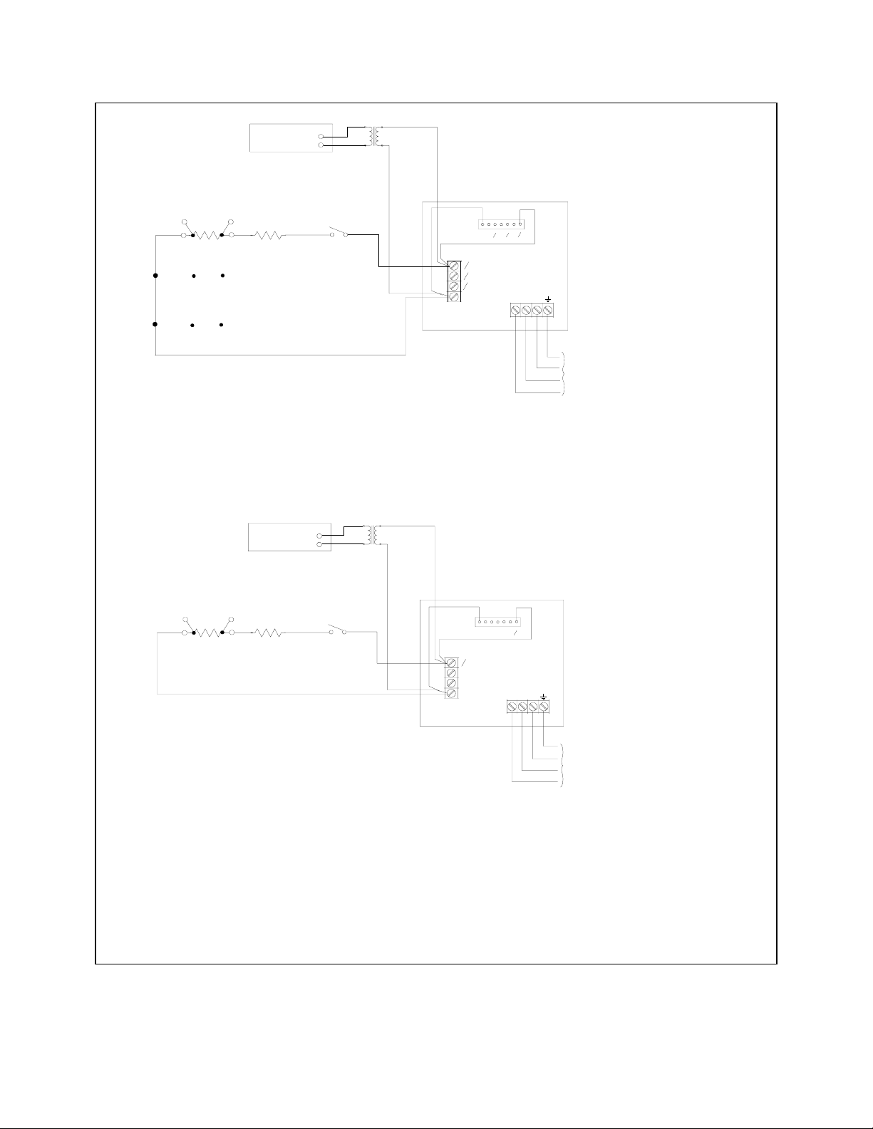
HP3458A
DMM
130
NOTE: Be sure to move sense lead to phase
under test or connect sense leads
to all three phases.
Rs
Rl
S1
Rl = 60 OHM @ 300V OUTPUT >1500W
15 OHM @ 150V OUTPUT >1500W
Rs = Current Monitor resistor - move for
testing current in phase 2 & 3
HP3458A
DMM
l
Rs
Rl
S1
SENSE
O1O2O3
6834B
L1 L2
L3
O1
O2
O3
COM
COM
AC INPUT 3 phase
180-254 VAC line to line
or
360-440 VAC lin e to li ne
TEST SETUP for 6834B
1
30
NOTE: Sense leads connections
reversed on 6843A
SENSE
O1
COM
O1
COM
6814B or
6843A
L1
L2
L3
Rl = 7.5 OHM or 30 OHM for 6814B
5 OHM or 20 OHM for 6843A
see performance test for correct value
Rs = Current Monitor resistor
TEST SETUP for 6814B / 6843A
*Note: Replace HP3458A DMM with HP5316B Counter for frequency test.
Replace HP3458A DMM with HP8903A Harmonic Analyzer for distortion test
Switch is for convience, not required.
Figure 2-1. Verification Test Setup
AC INPUT 3 phase
180-254 VAC line to line
or
360-440 VAC line to line
Performance Tests
17
Page 18

HP3458A
DMM
Rs
Rl
S1
Rl = 60 OHM @ 300V OUTPUT >1500W
15 OHM @ 150V OUTPUT >1500W
Rs = Current Monitor resistor - move for
testing current in phase 2 & 3
HP3458A
DMM
SENSE
O2O3
COM
O1
O2
O3
COM
O1
6834B
L1
L2
L3
TEST SETUP for 6834B
NOTE: Sense lead connections
reversed on 6843A
AC INPUT 3 phase
180-254 VAC line to line
or
360-440 VAC line to line
18
Performance Tests
Rs
Rl
Rl = 7.5 OHM or 30 OHM for 6814B
5 OHM or 20 OHM for 6843A
see perfor mance test for correct v alue
Rs = Current Monitor resistor
S1
SENSE
COM
O1
COM
TEST SETUP for 6814B / 6843A
Figure 2-2 Verification Test Setup
O1
6814B or
6843A
L1
L2
L3
AC INP UT 3 phas e
180-254 VAC line to line
or
360-440 VAC line to line
Page 19

3
Troubleshooting
Shock Hazard. The troubleshooting procedure in this chapter must be performed with power applied and
protective covers removed. These procedures should be done only by trained service personnel aware of
the hazard from electrical shock.
This instrument uses components that can be damaged or suffer serious performance degradation due
to ESD ( electrostatic discharge ). Observe standard antistatic precautions to avoid damage to
components ( see Chapter 1 ).
Introduction
Localizing the Problem
This chapter provides troubleshooting and repair information for the Agilent 6814B, Agilent 6834B AC Power Source and
Agilent 6843A RTS. Before beginning the troubleshooting procedures, make certain the problem is in the AC Power Source
and not with an associated circuit, the GPIB controller, or the ac input lines. Without removing the covers, you can use the
verification tests in chapter 2 to determine if the AC Power Source is operating normally.
Test Equipment Required
List of Equipment
Table 3-1 lists the equipment required to perform the troubleshooting procedures given in this chapter.
Table 3-1. Test Equipment Requirements for Troubleshooting
Equipment Characteristics Model
GPIB Controller Communicate with AC Source via GPIB or
RS232
Digital Voltmeter Check voltages / resistances Agilent 3458A or equivalent
Oscilloscope Observe waveforms Agilent 54504A or equivalent
Current Shunt Check output current 0.01 ohm 10 watt
Logic Probe Check data lines Agilent 545A or equivalent
HP Series 200/300 Controller
or Equivalent.
Troubleshooting Procedure
Table 3-2 gives the troubleshooting procedures to isolate a fault to a circuit board or particular circuit. See figure 6-l for the
location of the circuit boards.
Using *TST? Query
The AC Power Source executes a partial selftest by sending the GPIB selftest query command *TST?. The command
returns a value of zero if all tests pass. Otherwise, the command returns the error code of the first test that failed.
Troubleshooting
19
Page 20

Firmware Revisions
The model number and then the firmware revision is displayed on the front panel for approximately l0 seconds when unit is
first turned on. The firrnware revision is also accessible via the GPIB using the *IDN? query. The following sample
AgilentBASIC program does this.
10 ALLOCATE L$[52]
20 OUTPUT 705;"*IDN?"
30 ENTER 705;L$
40 DISP L$
50 END
The computer will display the string "HEWLETT-PACKARD,<model >,0,<revision>".
ROM Replacement or ROM Update
Instruments that are being initialized for the first time or have suffered non-volatile memory corruption should be initialized
with the front panel EEINIT command. To initialize the unit, perform the following:
1. Turn the unit on, then do the front panel CAL ON command.
2. Press 0 and 9 keys simultaneously. EEINIT <model> should now be displayed.
3. Scroll to the correct model number and press ENTER.
If the command is successful, the front panel display will go through a normal power-on sequence.
It is possible to update to newer ROM versions without destroying the calibration data. To update the unit to newer ROM
revisions, perform the following.
1. Turn input power off, remove the old ROMs and install the new ROMS.
2. Turn the unit on, then do the front panel CAL ON command.
3. Press 0 and 9 keys simultaneously, then scroll to the ROMUPD command.
4. Scroll to the correct model number and press ENTER.
If the command is successful, the front panel display will go through a normal power-on sequence. If "OUT OF RANGE"
error is displayed, then the instrument will have to be re-initialized with the EEINIT command and re-calibrated. This can
occur if the instrument was previously initialized with a QA firmware revision ( QA.xx.xx ), or if non-volatile memory has
become corrupted for any reason.
20
Troubleshooting
Page 21

Calibration Configuration Switch
An internal set of switches control access to calibration commands. The switches are located on the A8 DSP board and are
accessible by removing the top cover. Switches 1 and 2 set the calibration configuration. The three positions are:
Normal Cal This is the default switch position. The calibration functions are accessible after entering a
numeric password. The default password is 0 and is changeable by the user.
Clear Password The calibration password is reset to 0 and the remote programming language is set to SCPI.
This option is useful if the user has forgotten the password.
Inhibit Cal In this position the calibration of the power source cannot be changed. All calibration
commands are disabled. If the CAL ON command is sent with the switch in this position, an
Out Of Range error will be displayed on the front panel. This option is useful in installations
where calibration access is guarded by instrument seals.
Table 3-2. Specific Troubleshooting Procedures
Step Symptom Corrective Action
1.
2.
3.
rl- Re-initialize unit and re-calibrate. If unit still has RAM error, replace A8 DSP board. To re-initialize unit turn CAL ON,
then press 0 and 9, simultaneously. Press scroll key to model number, then press Enter. When unit is re-initialized all
CAL data, user-defined WAVEFORM data, and LIST data is erased.
r2 -Replace A8 DSP board.
No output voltage / front panel display and fan off go to table 3-3
No or limited output / front panel display and fan on go to figure 3-2
Turn-on Self Test Errors
Error l Non-volatile RAM RD0 section checksum failed Rl
Error 2 Non-volatile RAM CONFIG section checksum failed Rl
Error 3 Non-volatile RAM CAL section checksum failed Rl
Error 4 Non-volatile RAM WAVEFORM section checksum failed Rl
Error 5 Non-volatile RAM STATE section checksum failed Rl
Error 6 Non-volatile RAM LIST STATE section checksum failed Rl
Error l0 RAM selftest r2
Error 11 to 18 DAC self tests, l through 8 r2
Troubleshooting
21
Page 22

Troubleshooting Hints
1. Read all troubleshooting instructions before attempting to troubleshoot the unit.
2. If the AC Power Source operates properly but does not deliver full output power capability, check the ac input mains
fuses located on the rear panel.
3. The amplifiers, ( Al, A2, A3 ) may be interchanged in identical models for troubleshooting purposes. The Agilent
6814A, 6834A, and 6843A models Al, A2, A3 amplifiers cannot be used in the Agilent 6814B or 6834B models. See
Chapter 5, Replaceable Parts, for correct replacement amplifier.
4. The Agilent 6814B uses amplifiers Al and A2 and the 6843A uses amplifiers A1, A2 and A3 connected in parallel at
the output. Drawings show the connections and schematics for the Agilent 6834B 3 phase unit. When troubleshooting
the Agilent 6814B, the A3 amplifier and its associated parts are deleted from specific circuit boards.
5. Troubleshooting the A9 option 400 ( 380 to 460 volt ) Input PS is not recommended at this time. This is a 500 Vdc to
300 Vdc step down switching regulator and contains hazardous voltages.
Switching Amplifier Output Balance Adjustments
If the switching amplifiers ( A1, A2 or A3 ) are replaced phase B and C amplifier gains may require adjustment so they
better match that of phase A and current share equally when paralleled as a single phase output.
6834B Amplifier Balancing
1. With ACS off, temporarily short A5TP1 to A5TP2 on the A5 Relay board (this deactivates the paralleling relays).
2. Turn on ACS, program the output for single-phase operation, 300V, 60Hz, no load.
3. Measure the voltage from phase A output to common and from phase B output to common.
4. Adjust the phase B gain pot, A2A2R104, until phase B output matches phase A output to within 50 millivolts.
5. Measure the phase C output to common.
6. Adjust the phase C gain pot , A3A2R104, until phase C output matches phase A output to within 50 millivolts.
7. Turn off ACS and remove the short from TP1 to TP2.
6814B Amplifier Balancing
1. Turn off ACS, remove phase B amplifier. Turn on ACS. Program output voltage to 300V, 60Hz, no load.
2. Measure and note drive voltage on A6 Servo board at A6TP5 with respect to A6TP1.
3. Turn off ACS, remove phase A amplifier, install phase B amplifier in phase B slot. Turn on ACS. Program output
voltage to 300V, 60Hz, no load.
4. Measure drive voltage at A6TP3 as before. Adjust phase B gain pot A2A2R104 for same drive voltage as noted in step
2, plus or minus 2 millivolts.
5. Turn off ACS, re-install phase A amplifier in phase A slot.
6843A Amplifier Balancing
1. Turn off ACS, remove phase B and C amplifiers. Turn on ACS. Program output voltage to 300V, 60Hz, no load.
2. Measure and note drive voltage on A6 Servo board at A6TP3 with respect to A6TP1.
3. Turn off ACS, remove phase A amplifier, install phase B amplifier in phase B slot. Turn on ACS. Program output
voltage to 300V, 60Hz, no load.
4. Measure drive voltage at A6TP3 as before. Adjust phase B gain pot A2A2R104 for same drive voltage as noted in step
2, plus or minus 2 millivolts.
5. Turn off ACS, remove phase B amplifier, install phase C amplifier in phase C slot. Turn on ACS. Program output
voltage for 300V, 60Hz, no load.
6. Measure drive voltage at A6TP3 as before. Adjust phase C gain pot A3A2R104 for same drive voltage as noted in
step 2, plus or minus 2 millivolts.
7. Turn off ACS, re-install phase A and phase B amplifiers in their respective slots.
22
Troubleshooting
Page 23

Table 3-3. AC Power Source Troubleshooting Procedures
DANGER
Lethal voltages are present when
Instrument covers are removed.
Step Procedure Indication Action
1
Turn off ac mains, disconnect load, and
configure unit for local sensing.
2
3
4
5
Turn on unit and verify that ac power is on
by observing if front panel display is on and
fans are on.
Turn off power supply and remove top cover
as follows:
Remove 9 screws from top and 3 screws from
each side of unit.
Lift cover straight up being careful of lip on
front of cover.
Turn on supply and listen for clicking sound (
relays energizing ) on A9 Input assembly.
** See table 3-7 A14 Option 400 Bias PS
verification
Relays energize but no front panel display
and no fans. 300 Vdc on Cl.
** See table 3-4 A9 200/208 Input PS
verification & table A10 Auxiliary PS
verification.
_______________________________
Option 400 500 Vdc across C9 &
C10 300 Vdc on C1.
** See table 3-5 A9 Option 400 Input PS
verification.
No front panel, no fans, no
relay click ?
No relay click, relays do not
energize?
300 Vdc present ?
_____________________
500 Vdc present ?
300 Vdc present ?
Check F1, F2, F3 on rear
panel.
See fig 6-3 & 6-4
Check A9 1/4 amp fuse.
Check 24 volt bias Option
400 models
See fig 6-6,6-9&6-10 Check
A14 Fl, F2, F3 Check 24
volt bias
No 300 Vdc then
See fig 6-4 Check CR1,
A9F2,F3,F4 A9K1,K2,K3
300 Vdc OK
See fig 6-7 & 6-8
Check A10F1
____________________
No 500 Vdc then
See fig 6-6 Check CR1,
A9F2,F3,F4 A9K1,K2
Check 24 V from A14
assembly
No 300 Vdc then
Check bias voltages from
A14 assembly
Replace A9 assembly
6
Relays energize, fans are on, but no front
panel display.
+5VDC @ A10J6 ? See fig 6-7 & 6-14
Check voltages at A10J6
Check +5V at A8J724-7 to
A8J724-2,4 common
Troubleshooting
23
Page 24

Table 3-3. AC Power Source Troubleshooting Procedures (continued)
Step Procedure Indication Action
7
8
9
Relays energize, fans are on, but no front
panel display. Press the [ Shift ] key a couple
of times.
One or more outputs are missing.
The following procedures will attempt to
isolate the defective assembly by tracking the
bias voltages, ac program signal or ac output
signal.
Front panel display on, fans on.
Program VOLT 100, CURR:LEV 3, Output On using front panel keypad
for following procedures:
Tracking ac program signal.
See figure 3-2 AC Programming Signal Path.
Shift annuniciator on front
panel toggles.
300 Vdc on Cl. Yes
300 Vdc on C1. No
All bias voltage
present see fig 6-7. No
Check A8 DSP assembly.
See figure 6-14
If 1.1 Vrms not present replace
A8DSP assembly
Check +5Vhpib and +/-15V
at A10J1, J2, J3.
Check communication from
A8 DSP to A11 front panel.
A8 DSP assembly may be
defective.
Check A4F1,F2,F3 Fuses
Verify A9 Input PS see
table 3-4 or 3-5. If option
400 model also verify A14
bias see table 3-7.
Verify all bias voltages are
present. See table 3-6.
Measure 1.1 Vrms for
Phase 1 A8U740-9
Phase 2 A8U770-9
Phase 3 A8U774-9
Common is J724-2,4.
10
Tracking AC output signal.
Also see Table 3-9 to verify A5 Relay/Filter
assembly.
CAUTION – HIGH VOLTAGE
To verify amplifier output connect test leads,
Check A6 Servo assembly.
See figure 6-15
If 1.6 Vrms not present replace
A6 Servo assembly.
Check A5 Relay assembly.
Relays A5K5,A5K7 and
A5K8 defective ?
.
A1,A2,A3 amplifier
assemblies are good if voltage
Measure 1.6Vrms at
Phase 1 A6TP-3
Phase 2 A6TP-5
Phase 3 A6TP-7
Common at A6TP-1
Check 100 Vrms at
Phase 1 A5TB1-1
Phase 2 A5TB1-3
Phase 3 A5TB1-4
Common at A5TB1-5
If 100 Vrms not present
Then
Measure 100 Vrms at
Phase 1 A5L1
Phase 2 A5L2
Phase 3 A5L3
Common at A5TP-8
Measure approx. 34 Vrms
between:
24
Troubleshooting
Page 25

One to outside end of C1 and the other to
outside end of C3. ( outside end of capacitor
is end toward edge of heatsink )
is present at C1/C3
connections ( measure 100
Vrms with 300 Vrms
programmed )
A1C1 and A1C3
A2C1 and A2C3
A3C1 and A3C3
With 100 Vrms
programmed.
Verify A4 mother board
Note: See Switching Amplifier Balancing on
page 22.
Table 3-4. A9 208/208 Input Power Supply Troubleshooting
Procedure Action
See figure 6-3 and 6-4 for test points and schematic.
Surge Limit Circuit 1. Measure resistance from Jl-l to Jl-7 or Jl-2 to Jl-8 or Jl-3 to Jl-6.
Resistance must be greater than 100 k ohms.
2. Apply 208 volts 50/60 Hz between E4 and E7.
3. Measure resistance from Jl-l to Jl-7 or Jl-2 to Jl-8 or Jl-3 to Jl-6.
Resistance must be greater than 20 ohms.
Bias Voltages 1. Apply 208 volts 50/60 Hz between E4 and E7.
2. Voltage from ZR1 cathode (+) to TP1 (-) is between 23 and 25.5 Vdc.
3. Voltage from TP3 (+) to TP1 (-) is between +11.5 and 12.5 Vdc.
4. Voltage from ZR2 cathode (+) to TP4 is between 20 and 22 Vdc.
5. Voltage from ZR3 anode (+) to TP4 must be between –20 and -22 Vdc.
UVOV Detector 1. Apply 208 volts 50/60 Hz between E4 and E7.
2. Apply 300 Vdc (+) to El, (-) to E2. Verify voltage from U6-7(+) to TPI(-) is greater
than 9 Vdc.
3. Lower 300 Vdc to 220 Vdc. Verify that voltage at U6-7 is less than 1 Vdc.
4. Raise 300 Vdc to 395 Vdc. Verify that voltage at U6-7 is less than 1 Vdc.
common mode choke
continuity. See figure 6-13 for
location of chokes.
If voltage is present at
amplifier output ( C1/C3
connections) but not on A5
assembly check A5 assy.
Phase Loss Detector 1. Apply 208 volts 50/60 Hz between E4 and E7.
2. Verify that voltage from U4-7(+) to TP1(-) is less than 1 Vdc.
3. Apply 300 Vdc from Jl-l(+) to Jl-2(-). Verify that voltage from U4-7 to TP1(-) is greater
than 9 Vdc. Remove 300 Vdc.
4. Apply 300 Vdc from Jl-2(+) to Jl-3(-). Verify that voltage from U4-7 to TP1(-) is greater
than 9 Vdc. Remove 300 Vdc.
5. Apply 300 Vdc from Jl-3(+) to Jl-l(-). Verify that voltage from U4-7 to TP1(-) is greater
than 9 Vdc. Remove 300 Vdc.
Table 3-5. A9 Option 400 (400V) Input Power Supply Troubleshooting
Caution: A 500Vdc power source plus external capacitors and inductors are required to verify the operation of the A9
option 400 volt AC Input assembly. For safety concerns only check fuses A9F1, A9F2 and A9F3. If this does not resolve
the concern then replace the A9 option 400 AC Input assembly.
Troubleshooting
25
Page 26

Table 3-6. A10 Auxiliary Power Supply Troubleshooting
Procedure Action
See figures 6-7 and 6-8 for test points and schematic.
Control Circuits 1. Apply 20 Vdc between TP7(+) and TP1(-).
2. Verify waveform at TP2 to TP1. 0 V to >15 V at approximately 60 kHz, duty cycle
40% to 50%.
3. Check drive to Ql and Q4 . Connect scope common to CR13 anode, verify waveform
at gate drive resistors R10 and R28 is swinging between +12Vpk and –12Vpk at
approximately 60 kHz, duty cycle 40 to 50%.
Outputs 1. Apply 20 Vdc between TP7(+) and TP1(-). Add a 10 ohm 25 W resistor across R13.
2. Apply 300 Vdc between Jl-1,2 (+) to Jl-5,6 (-).
3. Verify the 15 SW1 voltage across R13 is between 14.5 and 15.5 Vdc.
4. Verify the +5 GPIB voltage across R18 is between 4.8 and 5.2 Vdc.
5. Verify the +5V SEC voltage across R33 is between 4.2 and 5.2 Vdc.
6. Verify the fan voltage from J3-1 (+) to J3-5 (-) is between 14.6 and 15.8 Vdc.
Short J4-6 to J3-5 fan voltage should now be between 17.4 and 18.9 Vdc.
7. Verify the +15 analog supply across R43 is between 14.3 and 15.5 Vdc.
8. Verify the –15 analog supply across R48 is between 14.3 and 15.5 Vdc.
*A lower input voltage ( <300 Vdc ) can be used but the expected output voltages must
be recalculated.
Table 3-7. A14 Option 400 Bias Power Supply Troubleshooting
Procedure Action
See figure 6-9 and 6-10 for test points and schematic.
Outputs 1. Apply 342 V 50/60 Hz between J2-1 and J2-4.
2. From TP1 (Lo) (Jl-7 ) to Jl-8 measure 26 Vdc +/- 2V.
3. From TP1 (Lo) (Jl-7 ) to Jl-6 measure 26 Vdc +/- 2V.
4. From TP2 (Lo) (Jl -3 ) to Jl -4 measure 19.3 Vdc +/- 2V.
5. From TP2 (Lo) (Jl-3 ) to Jl-2 measure -19.3 Vdc +/- 2V.
6. From TP3 (Lo) (J I -11 ) to J1 -1 0 measure 26 Vdc +/- 2V.
7. From TP2 (Lo) (Jl-3 ) to Jl-12 measure -26 Vdc +/- 2V.
*A lower input voltage ( <342 Vac ) can be used, but the expected output voltages must
be recalculated.
26
Troubleshooting
Page 27

Table 3-8. A4 Mother Board Troubleshooting
Procedure Action
See figure 6-13 for test points.
Inputs
Continuity check
Procedure Action
Range relays Program VOLT 50, CURR:LEV 3, Output On.
The following voltage tests verify that the correct input operational voltages are available
to the A4 mother board. To test for these voltages, remove the Al, A2 and A3 amplifier
assemblies.
The +300 Vdc and 300 Vdc return are shown on Fig 6-13.
The following input voltages appear at J2, J4 and J6.
IA phase A high IB phase A common
2A +5V sec 2B *OVT
3A 3B D common
12A common 1 12B common 1
13A -15VSW 13B -15VSW
15A + 15VSW 15B +15VSW
16A + 15VSW1 16B + 15VSW1
Verify common mode inductors ( L1 thru L6 ) continuity. See A4 Mother Board Parts
Location on Figure 6-13.
Table 3-9. A5 Relay / Filter Board Troubleshooting
See figure 6-11 and 6-12 for test points.
Program high range: Measure 25 volts from J2-1 to J2-3, J2-2 to J2-4, J2-5 to J2-7,
J2-6 to J2-8, J2-9 to J2-11 and J2-10 to J2-12.
Program low range: Measure 50 volts from J2-1 to J2-3, J2-2 to J2-4, J2-5 to J2-7,
J2-6 to J2-8, J2-9 to J2-11 and J2-10 to J2-12.
Output enable / disable
Relays
Sense relays Program ACL:INT: Measure greater than 10 megohms from R43 to K5 common, R44 to
Measure 50 volts from TB1-1 to TB1-6, TB1-3 to TB1-6 and TB1-4 to TB1-6. If
voltages are not available, test voltage between relays K5, K7, K8 common terminal to
determine defective relay.
K7 common, R45 to K8 common and R46 to K9 common.
Program ACL:EXT: Measure approximately 105 Kohms from R43 to K5 common, R44
to K7 common, R45 to K8 common and R46 to K9 common.
Troubleshooting
27
Page 28

28
Troubleshooting
Figure 3-1. Bias Voltage to Switching Amplifier Assemblies
Page 29

A8 DSP Assembly
A6 Servo Assembly
A4 Mother Assembly
Remove A1 A2 A3
to access these connections
Phase A U740-9
Phas6 B U770-9
Phase C U774-9
J722-5
J723-11
J723-17
J2-5
J2-11
J2-17
TP1
TP3
TP5
TP7
J4-1 P1-1
J4-5 P1-5
J4-3 P1-3
Figure 3-2. AC Programming Signal Path
J2-1A Sig A Hi
J2-1B
J4-1A Sig B Hi
J4-1B
J6-1A Sig C Hi
J6-1B
Sig A com
Sig B com
Sig C com
Troubleshooting
29
Page 30

Page 31

Principles of Operation
Introduction
Figure 4-1 ( at end of this chapter ) is a block diagram showing the major circuits within the ac source. The ac source
consists of the following modules:
Al, A2, A3 Switching Amplifiers Modules
A4 Mother Board Assembly
A5 Range Relay and Filter Assembly
A6 Servo ( Control ) Assembly
A7 IEEE488 ( GPIB ) & RS232 Interface Assembly
A8 Digital Signal Processing ( DSP ) Assembly
A9 Input Power Assembly
A10 Auxiliary Power Supply Assembly
Al 1 Front panel Assembly
A12 Input Filter PC Assembly
A13 Bridge Capacitor Filter Assembly
A14 Bias Power Supply ( option 400 only )
General Description
4
The 3 phase input power is connected to TBl on the rear panel, then routed through Fl, F2 and F3 to the RFI filter, FLI, to
relay Kl. The 3 phase input power is also connected to the A9 Input power assembly. When relay Kl closes the 3 phase
input is connected to power rectifier CRl, Ll and Cl to create 300 Vdc required by the power amplifiers Al, A2 and A3. The
amplifier assemblies in concert with the output filter and range relays produce the programmed waveform at the
programmed frequency and voltage. The 300 Vdc is also used by the A10 Auxiliary power supply board to produce the bias
voltages required by support circuits.
A1, A2, A3 Switching Amplifier Modules
The switching amplifier modules consist of a heat sink assembly, control board and power board. The 3 amplifier modules
are identical and can be interchanged for troubleshooting assistance. The amplifier assemblies can only be replaced as a
complete assembly, they are not repairable to the component level. The Agilent 6814B uses 2 amplifier assemblies
connected in parallel to provide 3000 watts single phase AC output power. The Agilent 6834B uses 3 amplifier assemblies
connected in a
3-phase configuration with each amplifier providing 1500 watts AC output power per phase. The 6843A uses three
amplifiers connected in parallel to provide 4800 watts single phase AC output power. When an amplifier assembly is
replaced it will be necessary to balance the amplifier, see paragraph on page 3-4 Switching Amplifier Output Balance
Adjustments. Amplifiers from [ 6814A, 6834A ] or [ 6843A ] or [ 6814B, 6834B ] Models are NOT INTERCHANGABLE.
See Chapter 5 Replaceable Parts listing for correct replacement assembly.
A4 Mother Board Assembly
The A4 mother board interconnects the Al, A2 and A3 amplifier assemblies with the A6 servo assembly, the 300 Vdc rail
voltage and the +/-15 Vdc bias supply. There are 10 amp fuses located in the +300 Vdc line to each amplifier assembly. The
Agilent 6814B and 6834B A4 assemblies are not interchangeable.
Principles of Operation
31
Page 32

A5 Relay Range / Sense Assembly
The A5 assembly consists of the output voltage filters, the output voltage range relays A5Kl, A5K2 and A5K3, the output
voltage disconnect relays A5K5, A5K6, A5K8 A5K9 and remote sense relays A5K4, A5K7 and all associated circuits. It
also interconnects the A7 GPIB/RS232 assembly, A11 front panel assembly and A8 DSP assembly with each other and the
trigger and DFI/RI signals. The Agilent 6814B and 6834B A5 assemblies are not interchangeable.
A6 Servo ( Control ) Assembly
The A6 servo or control assembly consists of the gate control circuits for the Al, A2 and A3 power amplifiers where
required. It also contains the voltage and current control amplifiers and receives the voltage and current programming
information from the A8 DSP assembly. It interconnects the range and protection signals between the A5 and A8
assemblies. This assembly is not component level repairable. The Agilent 6814B and 6834B A6 assemblies are not
interchangeable.
A7 IEEE488 (GPIB) / RS232 Interface Assembly
The A7 interface contains the CPU and logic circuits for communicating with either an GPIB or RS232 computer/controller.
This assembly is not component level repairable. This assembly is interchangeable with all AC power sources.
A8 Digital Signal Processing Assembly
The A8 DSP board contains the CPU, ROMs, Digital to Analog and Analog to Digital circuits to control the output voltage
and output current settings. The A8 board also contains all the logic circuits for generating arbitrary waveforms, frequency
changes and phase control. At power on the DSP board performs a self-test and will report a failure via the front panel
display. This assembly is not component level repairable and is not interchangeable between an Agilent 6814B and 6834B.
A9 Input Power Assembly - ( 208 volt input )
The A9 input power assembly provides a current limit circuit to initially charge Cl to 300 Vdc, a phase loss detection
circuit, the undervoltage / overvoltage detection circuits, and +/- l5VSW to the A10 auxiliary power supply assembly. When
S1, on/off switch, is closed a single phase is used to power two bias transformers generating the +/-15 Vdc, 12 Vdc for the
protection circuits and 24 Vdc to the current limit relays Kl, K2 and K3. There are 4 fuses on the A9 board. Fuse A9F1 is in
series with Sl on/off switch, if A9F1 is open the Agilent 6834B will not function in any form. The remaining 3 fuses, A9F2,
A9F3 and A9F4 are in series with the current limit resistors and relays. If all 3 fuses are open the unit will not function and
if 1 or 2 fuses are open the phase loss status bit be true and full output power will not be available. This assembly is not
component level repairable except for fuses. This assembly is interchangeable between an Agilent 6814B and 6834B.
A9 Input Power Assembly - ( 400 volt input )
The A9 input power assembly provides a current limit circuit to initially charge C9 and C10 to 550 Vdc, a step-down
switching regulator to power the +300V on C1, a phase loss detection circuit and the undervoltage / overvoltage detection
circuits. When S1, on/off switch, is closed a single phase is used to power three bias transformers on the A12 Bias board,
The A12 Bias board provides +16 Vdc, +15 Vdc, -5 Vdc, 12 Vdc for the protection circuits and 24 Vdc to the current limit
relays Kl and K2. There are 3 fuses on the A9 board. The 3 fuses, A9F2, A9F3 and A9F4 are in series with the current limit
resistors and relays. If all 3 fuses are open the unit will not function and if 1 or 2 fuses are open the phase loss status bit be
true and full output power will not be available. This assembly is not component level repairable except for fuses. This
assembly is interchangeable between a 6814B and 6834B.
32
Principles of Operation
Page 33

A10 Auxiliary Power Supply
The 300 Vdc is used by the A10 board to generate the bias voltages. The 300 Vdc input line is fused by a 1 ampere
subminiature fuse, A10F1. The A10 supplies an isolated +5 Vdc for the A7 GPIB/RS232 interface board and A11 front
panel board. The + 15 VSW dc to the A4 mother board via J2, the +/-15V and +5Vsec to the A6 servo board via J4 and
+5V sec to the A8 DSP board via J5. It also supplies the 12-24 Vdc for the fan speed control. All secondary bias winding
are fused with 1 ampere subminiature fuses A10F2 through A10F7. This assembly is not component level repairable except
for fuses. This assembly is interchangeable between an Agilent 6814B and 6834B.
A11 Front Panel Display Assembly
The A11 assembly contains the display assembly, keypad, rotary pulse generators (RPG) and digital logic circuits, CPU and
ROM. This assembly is not component level repairable. This assembly is interchangeable between an Agilent 6814B and
6834B.
A12 Input Filter Assembly
The A12 assembly contains resistor / capacitor networks connected line to line to reduce any magnetic noise from being
conducted back into the AC input mains.
A13 Bridge Capacitor Filter Assembly
The A13 assembly contains capacitors and surge protectors connected line to line and a common mode inductor and surge
protector connected in series with the + 300 Vdc bus. The filter is connected to reduce conducted and radiated noise
generated by the three-phase rectifier.
A14 Bias Power Supply
This assembly is only used with the 400 volt input option. The A12 board provides the ac voltages required for the low
voltage regulators and the +24 Vdc for the current limit relays on the A9 board. It also provides the +/-15VSW to the A10
Auxiliary board. Fuse F1 for the +24 Vdc, a LED will light on the A12 board if F1 opens. Fuse F2 and F3 for the +24 Vdc
and + 16 Vdc. F4 and F5 for the +/-15VSW. F6 and F7 for the + 15 Vdc / -5 Vdc regulators. This assembly is
interchangeable between an Agilent 6814B and 6834B.
Principles of Operation
33
Page 34

Figure 4-1. AC Power Source, Block Diagram
34
Principles of Operation
Page 35

Replaceable Parts
Introduction
This section lists the replaceable electrical and mechanical parts for the Agilent 6814B and 6834B AC Power
Source/Analyzers and 6843A RTS.
Table 5-1. Agilent 6814B, 6834B & 6843A Replacement Assemblies
Reference Desig. Model / Input Option Agilent Part No. Description
ELECTRICAL PARTS
Al-A3 6814B, 6834B 5063-3415 Output Switching Amplifier Assembly
A1-A3 6843A 5060-9696 Output Switching Amplifier Assembly
A4 6814B 5060-9695 Mother Board Assembly
A4 6834B, 6843A 5060-9673 Mother Board Assembly
A5 6814B 06814-69001 Relay / Filter Assembly
A5 6834B 06834-69001 Relay / Filter Assembly
A5 6843A 06843-69021 Relay / Filter Assembly
A6 6814B 06814-69002 Servo ( Control ) Assembly
A6 6834B 06834-69002 Servo ( Control ) Assembly
A6 6843A 5060-9607 Servo ( Control ) Assembly
A7 6814B, 6834B 5060-3594 GPIB/RS232 Interface Assembly
A7 6843A 5063-2376 GPIB/RS232 Interface Assembly
A8 6814B 5063-3455 DSP ( 1P ) Assembly
A8 6834B 5063-3456 DSP ( 3P ) Assembly
A8 6843A 5063-2368 DSP ( 1P ) Assembly
A9 6814B,6834B,6843A #208 5060-9671 AC Input Assembly
A9 6814B,6834B,6843A#400 5060-9675 AC Input Assembly
A10 All Models 5060-9672 Auxiliary Power Supply Assembly
A11 All Models 5060-3596 Front panel PC Assembly
A12 6814B,6834B#208 5060-9689 Input Filter Assembly
A12 6814B,6834B#400 5060-9688 Input Filter Assembly
A13 6814B,6834B#208 5063-2390 Bridge Filter Capacitor Assembly
A13 6814B,6834B#400 5063-2391 Bridge Filter Capacitor Assembly
A14 6814B,6834B#400 5060-9687 Bias Power Supply Assembly
A15 6814B, 6834B 5060-3597 BNC Assembly
A11G1,G2 All Models 0960-0912 RPG
A8U724 All Models 1818-4441 SRAM
A4F1-A4F3 All Models 2110-0911 15A-500V ( Buss KLM-15 )
A7F1 " 2110-0665 1A-250V
A9F1 " 2110-0004 1/4A-250V
A9F2-A9F4 " 2110-0007 1A-250V Slo Blo
A10F1 " 2110-0991 2A-250V Subminature
A10F2 – A10F7 " 8159-0005 Zero Ohm Resistor
5
Replaceable Parts
35
Page 36

Table 5-1. Agilent 6814B, 6834B & 6843A Replacement Assemblies (continued)
Reference Desig. Model / Input Option Agilent Part No. Description
ELECTRICAL PARTS
All Models 0360-2848 AC Input Terminal Block
All Models 0360-2849 AC Output Terminal Block
All Models 0370-3298 Knob
All Models 1252-1488 4 Terminal DFI/RI Connector Plug
All Models 1252-3698 7 Terminal Sense Connector Plug
All Models 1510-0444 Terminal – ground rear panel
All Models 2110-0397 Fuse holder – rear panel
All Models 3101-3088 Switch
All Models 3160-0306 Fan – tubeaxial – 4”
All Models 3160-0929 Fan – blower – 6”
All Models 5001-6794 Blinder
All Models 5001-6796 Label, Front Panel Upper & Lower
All Models 5001-9810 Cover, Fuse Holders
All Models 5001-9811 Cover, AC Output Terminal Block
All Models 5001-9838 Cover, Top
All Models 5001-9839 Cover, Side
All Models 5001-9872 Cover, AC Safety w/cable clamp
6814B/6834B 5002-1503 Rear Panel
6843A 5001-9870 Rear Panel
All Models 5040-1698 Front Frame Lower
All Models 5040-1702 Keypad
All Models 5040-1703 Front Frame Upper
All Models 5041-8801 Foot
All Models 5063-2310 Rack Mount Slide Kit
All Models 5080-2333 Window
6814B,6834B 5080-2455 Label, Rear Panel
6843A 5080-2334 Label, Rear Panel
All Models 5962-0883 Guide, Quick Start
All Models 5962-0885 Card, Quick Reference
All Models 5962-0887 Guide, Users
All Models 5962-0889 Guide, Programming
6843A 5962-0831 Guide, EN61000-3-2, EN61000-3-3, 60555
FL1 All Models 9135-0493 Filter - RFI
6814B 06814-80002 6814B Nameplate ( Superbug )
6834B 06834-80002 6834B Nameplate ( Superbug )
6843A 06843-80001 6843A Nameplate ( Superbug )
Note: See figure 6-2 for front frame mechanical assembly
36
Replaceable Parts
Page 37

6
Diagrams
Introduction
This chapter contains drawings and diagrams for troubleshooting and maintaining the Agilent 6814B and 6834B AC Power
Source/Analyzers. Unless otherwise specified in the drawings, a drawing or diagram applies to all models and input voltage
options.
Table 6-1. General Schematic Notes:
1. All resistors are in ohms ± 1%, 1/8 W, unless otherwise specified.
2. All capacitors are in microfarads unless otherwise specified.
3. Unless otherwise noted, bias connections to integrated-circuit packages are as follows:
Common + 5 V
14-pin packages pin 7 pin 14
16-pin packages pin 8 pin 16
20-pin packages pin 10 pin 20
Diagrams
37
Page 38

A7 HPIB
A8 Digital Signal Pro cessor DSP
A6 Se rvo
CR1
K1
A5 Relay / Filter
A10 Aux power supply
A3 Output Switching Assembly
( not used on 6814A/B )
A4 mother board
A2 Outpuit Switching Assembly
F1
F2
A1 Output Switching Assembly
F3
L1
A11 Front Panel Assembly
A9 Input po wer
C1
6814B, 6834B, 6843A Mechanical Layout 208/230 Volt Input
A7 HPIB
A8 DSP Ass emb ly
CR1
A6 Se rvo
K1
A12 Bi as Powe r Supply
A5 Relay / Filter
A3 Output Switching Assembly
( not used on 6814A/B )
A2 Output Switching Assembly
A1 Output Switching Assembly
6814B, 6834B, 6843A Mechanical Layout 400 Volt Input
Figure 6-1. Mechanical Parts
A4 mother board
L1
A11 Front Panel Assembly
A10 Aux power supply
C9
L2
C10
A9 Input power
F1
C1
F2
F3
38
Diagrams
Page 39

Figure 6-2. 6814B, 6834B and 6843A Front Frame Assembly
Diagrams
39
Page 40

40
Diagrams
Figure 6-3. A9 208/230V AC Input Board Parts Location
Page 41

Figure 6-4. A9 208/230V AC Input Assembly Schematic
Diagrams
41
Page 42

42
Diagrams
Figure 6-5. A9 400V AC Input Board Parts Location
Page 43

Figure 6-6. A9 400V AC Input Assembly Schematic
Diagrams
43
Page 44

44
Diagrams
Figure 6-7. A10 Auxiliary Power Supply Board Parts Location
Page 45

Figure 6-8. A10 Auxiliary Power Supply Assembly Schematic
Diagrams
45
Page 46

46
Diagrams
Figure 6-9. A14 Bias Power Supply Board Parts Location
Page 47

Figure 6-10. A14 Bias Power Supply Assembly Schematic
Diagrams
47
Page 48

48
Diagrams
Figure 6-11. A5 Range/Output/Phase Relay Schematic
Page 49

Figure 6-12. A5 Range/Output/Phase Relay Driver Schematic
Diagrams
49
Page 50

PHASE C
1516
P2
1A 1B
L3
C Lo
E20
+300V
COM2
16A 16B
6
141822
10
OUT Lo
OUT Hi
26
30
L6
C Hi
E19
B Lo
E18
8
4
12
16
24
28
20
32
L5
B Hi
E17
P1
12
P2
P2
1A 1B
1A 1B
16A 16B
2526
P2
1
16A 16B
COM2
+300V
OUT Lo
OUT H i
A Lo
E16
A Hi
E15
+300V
COM2
6
141822
10
8
4
12
COM2
2
OUT Lo
OUT Hi
26
30
16
24
28
20
+300V
OUT Lo
32
OUT Hi
L4
COM2
E1
+300V
E2
L1 L2
+300V
COM2
6
141822
10
OUT Lo
OUT Hi
26
30
F1
50
Diagrams
PHASE A PHASE B
8
4
12
16
24
28
20
COM2
+300V
OUT Lo
32
OUT Hi
COMMO N MO DE INDUCTER S L1, L2, L3, L4, L5 and L6
MOUNTED ON FAR SIDE OF A4 MOT HER ASSEMBLY
F2
F3
Figure 6-13. A4 Mother Board Parts Location
Page 51

U715
U721
U735
U720
U723
U722
2
1
J724
1
J715
D COM
S700
U787
U711
U724
U712
U785
U774
U714
U737
12
U770
U783
U716
12
U741
U753
U781
U725
12
U740
U751
U736
U736
U776
U773
+ 5V
+5V
DAC out phase C
DAC out pha se B
DAC out pha se A
U755
D COM
+ 5V UNREG ( 8-9 Vdc )
J721
3
J746
U754
1
1
1
J723
1
J722
Figure 6-14. A8 DSP Board Parts Location
Diagrams
51
Page 52

+5VSEC +15V
TP 8
J5
TP 9
TP 5
J6
Phase 2
TP 1
COM
-15V
J4
TP 7
TP 3TP 10
Phase 3
Phase 1
J3
TP 4
TP 2TP 6
J2
J1
52
Diagrams
Figure 6-15 A6 Servo Board Test Point Location
Page 53

Index
A
AC Power Source modules ..........................................................................................................................................31
C
calibration configuration switch...................................................................................................................................21
change sheets .................................................................................................................................................................8
clear password
switch position........................................................................................................................................................21
commands
CAL ON command .................................................................................................................................................20
EEINIT command...................................................................................................................................................20
conductive table mat......................................................................................................................................................8
conductive wrist strap....................................................................................................................................................8
configuration switch
for calibration .........................................................................................................................................................21
current limiting resistors ........................................................................................................................................32, 33
current-monitoring resistor ............................................................................................................................................9
E
electrostatic discharge..............................................................................................................................................8, 19
error code, over GPIB..................................................................................................................................................21
ESD..........................................................................................................................................................................8, 19
F
fan speed control..........................................................................................................................................................33
fault isolation ...............................................................................................................................................................21
firmware revisions ...................................................................................................................................................8, 20
Form, performance test record .....................................................................................................................................13
fuses
Al0F1-F7 fuse.........................................................................................................................................................33
A9F1-F4..................................................................................................................................................................32
AC main fuses.........................................................................................................................................................23
F2, F3, F4, F5 .........................................................................................................................................................33
subminature fuses Al0F2, Al0F7 ............................................................................................................................33
G
general description.......................................................................................................................................................31
H
hazardous voltages.........................................................................................................................................................7
hazards
shock.......................................................................................................................................................................19
Index (continued)
Index
53
Page 54

I
*IDN query..................................................................................................................................................................20
inhibit cal
switch position........................................................................................................................................................21
initializing the unit.......................................................................................................................................................20
L
localizing problems......................................................................................................................................................19
M
manual backdating.........................................................................................................................................................8
manual changes sheet.....................................................................................................................................................8
manual revisions ............................................................................................................................................................8
measurement general techniques....................................................................................................................................9
microswitches
internal....................................................................................................................................................................21
modules
A10 auxiliary power supply....................................................................................................................................33
A11 front panel display assembly ...........................................................................................................................33
A12 input filter assembly........................................................................................................................................33
A13 bridge capacitor filter assembly ......................................................................................................................33
A14 bias power supply............................................................................................................................................33
A1, A2, A3 switching amplifier modules................................................................................................................31
A4 mother board assembly .....................................................................................................................................31
A5 relay range/sense assembly ...............................................................................................................................32
A6 servo control assembly......................................................................................................................................32
A7 IEEE-488 GPIB / RS-232 interface assembly...................................................................................................32
A8 digital signal processing assembly ....................................................................................................................32
A9 input power assembly..................................................................................................................................32, 33
interface assembly...................................................................................................................................................32
N
non-volatile memory corruption ..................................................................................................................................20
normal cal
switch position........................................................................................................................................................21
O
OUT-OF-RANGE error...............................................................................................................................................20
P
performance test record form.......................................................................................................................................13
performance test record sheets............................................................................................................................... 14-16
performance tests.........................................................................................................................................................10
procedures
troubleshooting .......................................................................................................................................................23
protective earth ground..................................................................................................................................................8
Index (continued)
54
Index
Page 55

R
ram error ......................................................................................................................................................................21
reinitializing unit..........................................................................................................................................................20
related documents ..........................................................................................................................................................7
resistor
current-monitoring ....................................................................................................................................................9
revisions.........................................................................................................................................................................8
ROM replacement........................................................................................................................................................20
ROM update ................................................................................................................................................................20
ROM versions..............................................................................................................................................................20
S
safety considerations..................................................................................................................................................3, 7
safety warnings ..............................................................................................................................................................7
serial number .................................................................................................................................................................4
serial number prefix.......................................................................................................................................................4
shock hazards...............................................................................................................................................................19
T
test equipment required............................................................................................................................................9, 19
tests
cv load effect...........................................................................................................................................................11
cv source effect.......................................................................................................................................................11
frequency programming..........................................................................................................................................10
harmonic distortion.................................................................................................................................................12
readback accuracy...................................................................................................................................................10
rms current accuracy...............................................................................................................................................12
voltage programming ..............................................................................................................................................10
troubleshooting
test equipment.........................................................................................................................................................19
troubleshooting hints....................................................................................................................................................22
troubleshooting procedure ...........................................................................................................................................19
troubleshooting table....................................................................................................................................................23
*TST? query ................................................................................................................................................................19
U
undervoltage / overvoltage detection circuits...............................................................................................................32
updating ROM versions...............................................................................................................................................20
using *IDN query.........................................................................................................................................................20
V
verification.....................................................................................................................................................................9
Index
55
Page 56

Manual Updates
The following updates have been made to this manual since the print revision indicated on the title page.
7/99
The Digital Voltmeter Characteristics on page 9 have been corrected.
The Output Balance Adjustments on page 22 have been updated.
Step 6 on page 23 has been corrected.
The note on the bottom of page 25 has been updated.
The fuses, rear panel, and rear panel label part numbers in table 5-1 have been updated (pp. 35-6)
11/99
The serial numbers on the title page have been updated.
The instrument identification section on page 4 has been updated.
Figures 2-1 and 2-1 have been updated.
The part number for FL1 has been added to table 5-1.
56
 Loading...