Infra-Red LED Driver IC for CCD Camera Module
General Description
ADT7110
The ADT7110 is a fixed frequency step-down
converter designed to drive Infrared LEDs in the
CCD camera module application.
And internal current limit circuit protect external
devices.
Features
• Input voltage range : 10.5V to 15V
• Current mode PWM controller with
integrated compensation components
• 350mA output load current available
• Built-in chip enable/disable function
• Built-in current limit protection
• 500kHz fixed frequency internal oscillator
• Small outline SOT-26 package (2.9mm x 1.6mm body)
6
4
5
A11
1
3
2
Package outline of the ADT7110
Applications
• Infrared LED driver for CCD camera
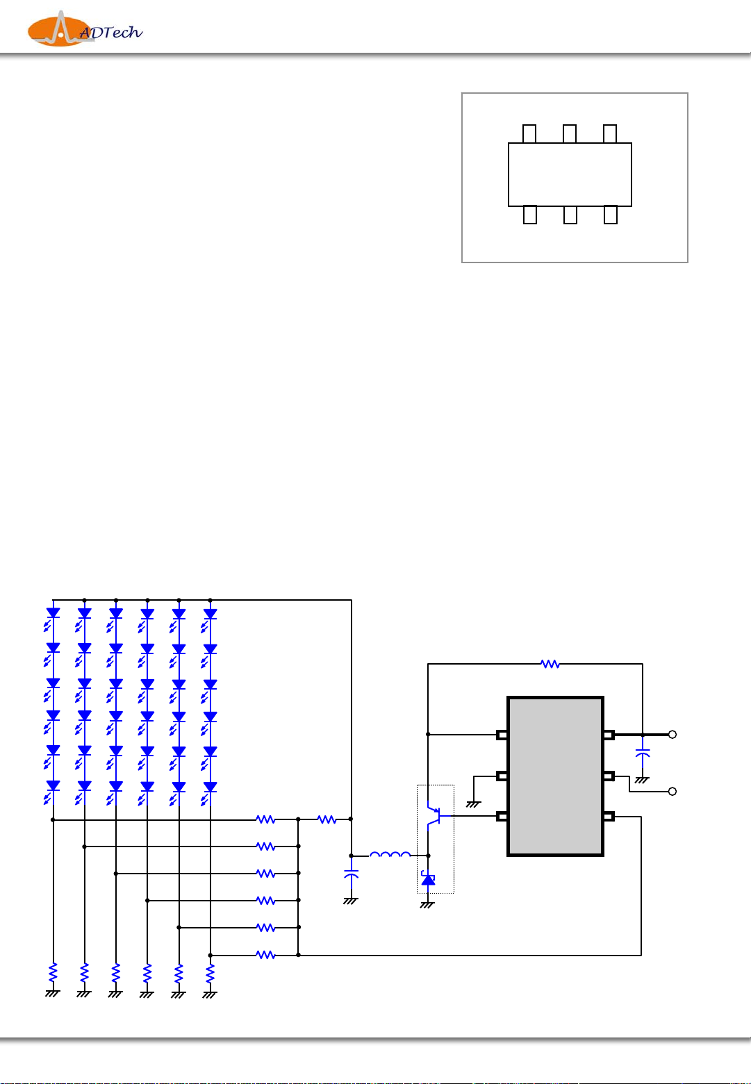
Typical Application Circuit
V
OUT
R
R
R
R
R
R
LED2
LED1
LED4
LED3
LED6
LED5
R
SE
RS
GND
VIN
A11
EN
VIN
C2
EN
R
FB2
R
FB1a
R
FB1b
R
FB1c
R
FB1d
R
FB1e
R
FB1f
L1
C1
U1
PWM
FB
V
FB
Mar. 12. 2009 / Rev. 0.1
* This specifications are subject to be changed without notice
1/4
http://www.ad-tech.co.kr

Infra-Red LED Driver IC for CCD Camera Module
Part List
Component Description Type Value
ADT7110
*1
U1
L1 Output filter inductor Chip inductor 47uH/590mA
C1 Output filter capacitor Tantalum capacitor 47uF/16V
C2 Bypass capacitor Tantalum capacitor 10uF/25V
R
SE
R
~ R
LED1
LED6
R
~ R
FB1a
FB1f
*3
R
FB2
*1 : For cost down , it is possible to use discrete component with a PNP transistor and a schottky barrier diode.
In this case, you make use the discrete components with proper electrical specification.
Table A shows the required key electrical limits. It is recommended to use PNP and schottky barrier diode
having equivalent specification in the Table A.
*2, *3 : To setting appropriate LED current, Refer to ‘Application Hints’.
Composite type with a PNP transistor
and schottky barrier diode
Current sense resistor Chip resistor 0.1Ω
*2
LED current ballast resistor Chip resistor , 1% 4.0Ω
Buck converter feedback loop
component
Buck converter feedback loop
component
IC FP103
Chip resistor 120㏀ (table 3)
Chip resistor , 1% 68㏀ (table 2)
Table A : Selection guide for the discrete components
Component Parameter Ratings Unit Remarks
PNP
Schottky
Barrier Diode
Collector to Emitter Voltage -23 V
Collector Current -2 A
Repetitive Peak Reverse Voltage 30 V
Average Rectified Current 700 mA
Package ; SOT-26, 2.9mm x 1.6mm body (units : mm)
Recommend
‘2SB1706’ by ROHM or Equivalent IC
Recommend
‘RSX101M-30’ by ROHM or Equivalent
Mar. 12. 2009 / Rev. 0.1
* This specifications are subject to be changed without notice
2/4
http://www.ad-tech.co.kr

Pin Configuration
Infra-Red LED Driver IC for CCD Camera Module
ADT7110
1
6
A11
2
3
5
4
Pin Description
Pin No. Name I/O Type Description
1
2
3
4
5
6
I : Input pin O : Output pin IO : Input/Output pin
P : Power pin G : Ground pin
A : Analog pin D : Digital pin
RS
GND
PWM
FB
EN
VIN
I A Current sense and provide voltage feed-forward.
- G Ground
O D Switching output.
I A Feedback voltage input
I D Device enable pin
- P Power supply input
Functional Block Diagram
EN
GND
FB
Internal
REG.
BIAS
Amplifier
REF
* This specifications are subject to be changed without notice
Error
+
-
gm
OSC
Set
∑
PWM
Comparator
-
+
Set
Current
Sense
Current
Limit
Control
Logic
VIN
-
+
-
+
Driver
RS
SW
Mar. 12. 2009 / Rev. 0.1
3/4
http://www.ad-tech.co.kr

Infra-Red LED Driver IC for CCD Camera Module
Absolute Maximum Ratings
Parameter Symbol Min. Typ. Max. Unit
ADT7110
Power supply voltage V
Power dissipation (Ta=70℃) (Note1) P
Storage temperature T
Junction temperature T
Thermal resistance
Dmax
STG
Jmax
Θ
IN
JA
- - 23 V
- - 265
-65 - +150
- - +150
- 301.2 - ℃/W
Note1. derate 301℃/W above +70℃.
Stresses beyond those listed under “Absolute Maximum Ratings” may cause permanent damage to the device.
These are stress ratings only, and functional operation of the device at these or any other conditions beyond those
indicated in the operational sections of the specifications is not implied. Exposure to absolute maximum rating
conditions for extended periods may affect device reliability.
Operating Ratings
Parameter Symbol Min. Typ. Max. Unit
Power supply voltage
Operating temperature T
Junction temperature T
Max. power dissipation (Ta=70℃)
*1 This spec. indicates that junction temperature of the device is under 125℃. In specific applications ,
this is recommended under this power dissipation specification.
*2 Minimum V
Maximum V
For using V
Table B : Maximum drive current as maximum V
V
(V) 16 17 18 19 20 21 22
IN
Drive current (㎃) 330 310 290 270 250 230 210
*2
*1
operating range is dependant to the V
IN
operating range can be extended. In this case, maximum drive current is limited.
IN
over 15V, refer to the Table B.
IN
V
IN
OPR
J
P
D
OUT
operating voltage.
IN
10.5 12.0 15.0 V
-20 - +85
- - +125
- - 180
voltage. ( VIN min. ≒ V
OUT
+ 0.5V)
㎽
℃
℃
℃
℃
㎽
Electrical Characteristics (Ta=25℃, VIN=12V, unless otherwise noted)
Parameter
Supply current, operating
Supply current, disable V(EN) = 0V - 90 200
V(EN), input voltage high - 2.4 - - V
V(EN), input voltage low - - - 1.2 V
PWM controller
Output drive current VIN ≤
Current limit - 550 - - ㎃
Efficiency IO =300㎃ - 85 - %
Oscillator frequency IO =300㎃ 350 500 625
Feedback voltage (V
) IO =300㎃ 2.16 2.21 2.26 V
FB
Mar. 12. 2009 / Rev. 0.1
V(EN) = 3.3V , IO =300㎃ - 6 9 ㎃
* This specifications are subject to be changed without notice
Condition MIN TYP MAX Unit Note
15V - 300 350 ㎃
4/4
㎂
㎑
http://www.ad-tech.co.kr

 Loading...