

Acer ACERMATE 920, ACERMATE 930 Annexe 2

& K DSWHU
System Board
The V50LA is a high-performance system board with a 64-bit
architecture. It supports the new Intel P54C, P54CQS, P54CS,
P54CT, and P55C CPUs running at 75/90/100/120/133/150 MHz and
utilizes the Peripheral Component Interconnect (PCI) local bus
architecture. The PCI local bus maximizes the system perform ance
by enabling high-speed peripherals to match the speed of the
microprocessor with its 120 MB or 132 MB per second transfer rate in
burst mode.
The board incorporates a Sound Blaster Pro-compatible audio
subsystem that consists of CD-audio, WaveTable, and fax/modem
line-in interfaces. A standard 1-MB video DRAM com es onboard and
is upgradable up to 2 MB. Two DRAM banks c omposed of f our 72-pin
sockets come with the board to support single- and double-density
SIMMs for a maximum system memory of 128 MB. The SIMM
sockets accommodate both the standard page mode and extended
data output (EDO) type SIMMs. The board supports a standard 256KB asynchronous or an optional 256-KB pipeline burst mode secondlevel cache.
The system board includes a 188-pin connector f or the slot board that
contains the PCI and ISA bus slots. The two onboard PCI- enhanced
IDE interfaces with a zero-wait state and 16.6 MB per second trans fer
rate support up to four IDE devices. Onboar d I/O interfaces c omprise
of two UART 16550 serial ports, a parallel port with ECP/EPP feature,
and PS/2 keyboard and mouse ports.
System Board 1-1

1.1 Major Features
The system board has the following major features:
A zero-insertion force (ZIF) socket for P54C, P54CTB, or
•
P54CS CPU
Two DRAM banks composed of four 72-pin SIMM sockets that
•
support 4/8/16/32-MB 60/70ns SIMMs
256-KB write-back asynchronous second-level cache
•
128-KB boot block mode Flash ROM for system and VGA BIOS
•
Two PCI-enhanced IDE interfaces that support up to four IDE
•
devices
System clock/calendar with 128 bytes CMOS RAM
•
Interfaces for CD-audio, fax/voice modem, and WaveTable
•
support
Standard 1-MB video DRAM onboard plus two upgrade sock ets
•
for up to 2-MB video memory
188-pin connector for PCI/ISA slot board
•
Feature socket for multimedia or Ethernet solution
•
External ports:
•
PS/2 keyboard and mouse ports
•
Two buffered high-speed serial ports
•
One ECP/EPP high-speed parallel port
•
Video port
•
1-2 User’s Guide
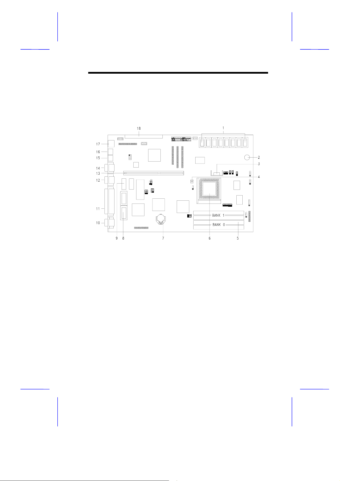
1.1.1 Layout
Figure 1-1 shows the locations of the system board major
components.
1 Second-level cache
2 Buzzer
3 CPU voltage regulator
4 Fan connector
5 SIMM sockets
6 321-pin ZIF CPU socket
7 3.3V battery
8 Video memory upgrade sockets
9 Onboard video memory
10 Video port
11 Parallel port
12 COM2
13 Slot board connector
14 COM1
15 PS/2 mouse connector
16 PS/2 keyboard connector
17 RJ-45 phone jack
18 Feature socket for multimedia
or Ethernet solution
Figure 1-1 System Board Layout
System Board 1-3
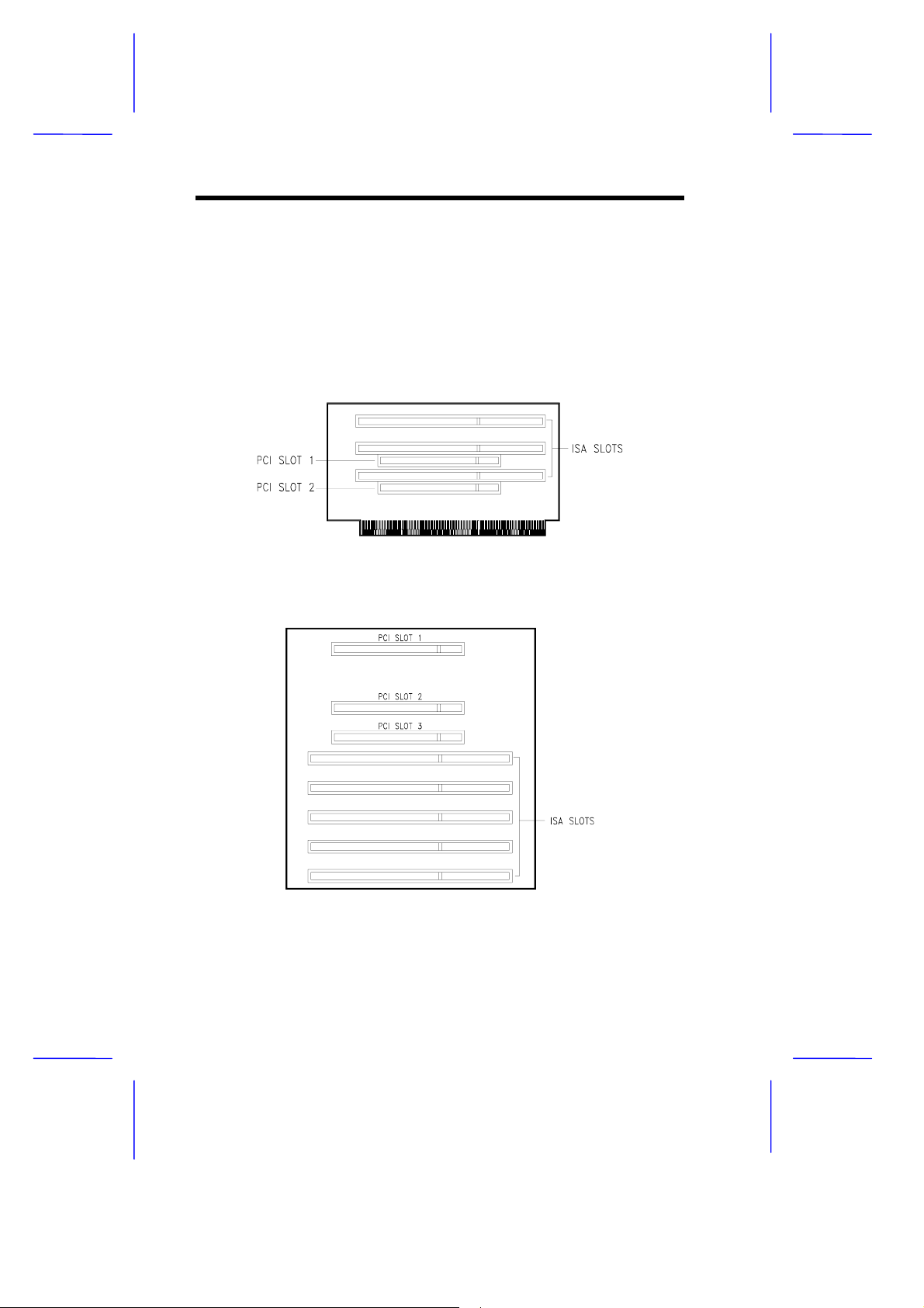
1.1.2 Slot Board
The system board comes with a slot board already installed. The slot
board carries the PCI and ISA bus slots for system enhanc ements and
future expansion.
The slot board may vary in size and layout depending on your syst em
housing. Figures 1-2 and 1-3 show the two kinds of slot boards.
Figure 1-2 2 -PCI/3-ISA Slot Board (for desktop systems)
Figure 1-3 3-PCI/5-ISA Slot Board
(for mini-tower systems)
1-4 User’s Guide
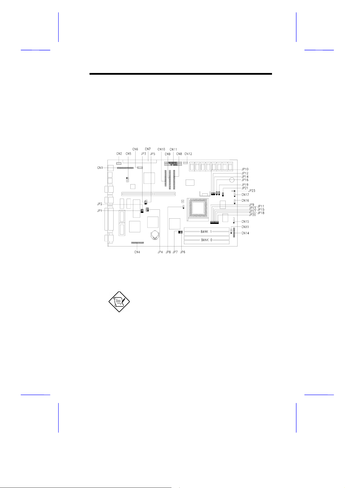
1.2 Jumpers and Connectors
1.2.1 Jumper and Connector Locations
Figure 1-4 shows the jumper and connector locations on the s ystem
board.
Figure 1-4 System Board Jumper and Connector Locations
Jumpers are prefixed “JP”. Connectors are
prefixed “CN”.
The blackened pin of a jumper represents
pin 1.
System Board 1-5

1.2.2 Jumper Settings
Table 1-1 lists the system board jumpers with their corresponding
settings and functions.
Table 1-1 System Board Jumper Settings
Jumper Setting Function
BIOS Type
JP1 1-2
Password Check
JP2 1-2
Boot Block Feature
1
JP3 1-2
BIOS ROM Type
JP5 1-2
CPU Core/Host Bus
Frequency
JP4 1-4
Second-level Cache
JP6, JP7 1-2*,1-2* 256 KB
2-3
2-3*
2-3*
2-3
3-4*
2-5*
3-6
*
For models with Acer BIOS
For models with OEM BIOS
Check password
Bypass password
(For Intel 28F001 only)
Enable Flash ROM boot block
feature
Disable Flash ROM boot block
feature
EPROM
Flash ROM (Intel 28F010, 28F001)
Flash ROM (SST 29EE010)
75/50 MHz
90/60, 120/60, 150/60 MHz
100/66, 133/66, 167/66 MHz
All other setting combinations are
reserved.
*
Default setting
1
The boot block feature works only for Intel 28F001 Flash ROM and requires JP5 to
be set to pins 2-3.
1-6 User’s Guide

Table 1-1 System Board Jumper Settings (continued)
Jumper Setting Function
CPU Type
JP8 1-2*
CPU Core / Local Bus
Clock Ratio
JP16, JP19
CPU Voltage
JP21 1-2*
LED Support
JP23 1-2
2-3
*
1-2
, 1-2*
1-2, 2-3
2-3, 1-2
2-3, 2-3
2-3
2-3*
Intel P54C or AMD K5
Cyri x M1
Intel P54C Intel P55C M1 and K5
3/2 3/1 3/2, 2/1, 3/1
2/1 2/1 1/1
3/1
5/2
3.3825V for VR and standard CPU type
3.5250V for VRE CPU type
For IDE and diskette drives
For IDE drive only
The jumpers JP10 ~ JP15 and JP17 are
always closed if there is no voltage regulator
module (VRM) present.
*
Default setting
System Board 1-7

1.2.3 Connector Functions
Table 1-2 lists the differ ent connectors on the system board and their
respective functions.
Table 1-2 Connector Functions
Connector Function
CN1 Audio-I/O board connector
CN2 Fax/voice modem connector
CN4 Video feature connector
CN5 WaveTable connector
CN6 CD-audio line-in connector
CN7 Feature connector for multimedia or
Ethernet solution
CN8 IDE channel 1
CN9 IDE channel 2
CN10 Diskette drive connector
CN11 Power connector
CN12 Standby power connector
CN14 Multifunction connector
CN15 IrDA connector
CN16 Hard disk drive LED connector
CN17 Hard disk drive LED connector
(generic)
CNX1 SMM switch/Reset switch
1-8 User’s Guide
 Loading...